EP3631361B1 - Integrated optical gyroscope with noise cancellation - Google Patents
Integrated optical gyroscope with noise cancellation Download PDFInfo
- Publication number
- EP3631361B1 EP3631361B1 EP18810298.2A EP18810298A EP3631361B1 EP 3631361 B1 EP3631361 B1 EP 3631361B1 EP 18810298 A EP18810298 A EP 18810298A EP 3631361 B1 EP3631361 B1 EP 3631361B1
- Authority
- EP
- European Patent Office
- Prior art keywords
- optical
- period
- signal
- ring
- path
- Prior art date
- Legal status (The legal status is an assumption and is not a legal conclusion. Google has not performed a legal analysis and makes no representation as to the accuracy of the status listed.)
- Active
Links
Images



Classifications
-
- G—PHYSICS
- G01—MEASURING; TESTING
- G01C—MEASURING DISTANCES, LEVELS OR BEARINGS; SURVEYING; NAVIGATION; GYROSCOPIC INSTRUMENTS; PHOTOGRAMMETRY OR VIDEOGRAMMETRY
- G01C19/00—Gyroscopes; Turn-sensitive devices using vibrating masses; Turn-sensitive devices without moving masses; Measuring angular rate using gyroscopic effects
- G01C19/58—Turn-sensitive devices without moving masses
- G01C19/64—Gyrometers using the Sagnac effect, i.e. rotation-induced shifts between counter-rotating electromagnetic beams
- G01C19/72—Gyrometers using the Sagnac effect, i.e. rotation-induced shifts between counter-rotating electromagnetic beams with counter-rotating light beams in a passive ring, e.g. fibre laser gyrometers
- G01C19/721—Details, e.g. optical or electronical details
- G01C19/722—Details, e.g. optical or electronical details of the mechanical construction
-
- G—PHYSICS
- G01—MEASURING; TESTING
- G01C—MEASURING DISTANCES, LEVELS OR BEARINGS; SURVEYING; NAVIGATION; GYROSCOPIC INSTRUMENTS; PHOTOGRAMMETRY OR VIDEOGRAMMETRY
- G01C19/00—Gyroscopes; Turn-sensitive devices using vibrating masses; Turn-sensitive devices without moving masses; Measuring angular rate using gyroscopic effects
- G01C19/58—Turn-sensitive devices without moving masses
- G01C19/64—Gyrometers using the Sagnac effect, i.e. rotation-induced shifts between counter-rotating electromagnetic beams
-
- G—PHYSICS
- G01—MEASURING; TESTING
- G01C—MEASURING DISTANCES, LEVELS OR BEARINGS; SURVEYING; NAVIGATION; GYROSCOPIC INSTRUMENTS; PHOTOGRAMMETRY OR VIDEOGRAMMETRY
- G01C19/00—Gyroscopes; Turn-sensitive devices using vibrating masses; Turn-sensitive devices without moving masses; Measuring angular rate using gyroscopic effects
- G01C19/58—Turn-sensitive devices without moving masses
- G01C19/64—Gyrometers using the Sagnac effect, i.e. rotation-induced shifts between counter-rotating electromagnetic beams
- G01C19/72—Gyrometers using the Sagnac effect, i.e. rotation-induced shifts between counter-rotating electromagnetic beams with counter-rotating light beams in a passive ring, e.g. fibre laser gyrometers
- G01C19/727—Gyrometers using the Sagnac effect, i.e. rotation-induced shifts between counter-rotating electromagnetic beams with counter-rotating light beams in a passive ring, e.g. fibre laser gyrometers using a passive ring resonator
Definitions
- the present invention relates to a gyroscope, and more particularly to an optical gyroscope.
- Gyroscopes are used in a variety of devices, such as smartphones, cars, aircrafts and the like for navigation. As is known, a tradeoff exists between the accuracy of a gyroscope and its size. For example, ring laser gyroscopes or fiber optic gyroscopes with relatively high accuracy are expensive and bulky. Micro electro-mechanical systems (MEMS) based gyroscopes are relatively small but lack precision.
- MEMS Micro electro-mechanical systems
- US Patent No. 4,658,401 describes a passive ring resonator laser gyro in which the clockwise and counterclockwise beams do not coexist in the resonator.
- the laser gyro employs thin film technology.
- the preferred laser is a gallium aluminum arsenide laser.
- Light from the laser is phase-modulated by means of a thin film electro-optic modulator comprising a channel waveguide disposed on an electrically active material and flanked by electrodes for modulating the phase of light from the laser.
- An electro-optic switch is provided for switching light from the laser to inject alternatingly clockwise and counterclockwise beams into the resonator.
- the resulting gyro is compact and simply implemented into an integrated, thin film package. Because the clockwise and counterclockwise beams do not coexist in the resonator, various beam interaction effects such as beats, backscatter and feedback into the laser are eliminated.
- An optical gyroscope in accordance with a first aspect of the present invention, includes an optical switch adapted to deliver a laser beam to a first path during a first half of a period and to a second path during a second half of the period, a first optical ring configured to deliver a first portion of the beam received from the first path in a clockwise direction during the first half of the period, and further to deliver a first portion of the beam received from the second path in a counter clockwise direction during the second half of the period, a second optical ring configured to deliver a second portion of the beam received from the first path in a counter clockwise direction during the first half of the period, and further to deliver a second portion of the beam received from the second path in a clockwise direction during the second half of the period, a first photodetector adapted to receive the beams delivered by the first and second optical rings during the first half of the period, a second photodetector adapted to receive the beams delivered by the first and second optical rings during the second half of the
- the optical gyroscope further includes a bandpass filter adapter to filter the first signal. In some embodiments, the optical gyroscope further includes a mixer adapted to downconvert a frequency of the filtered first signal to generate a baseband signal. In some embodiments, the optical gyroscope further includes a controller adapted to convert the baseband signal to a digital signal, and generate a signal representative of a degree of rotation of the optical gyroscope about an axis in response to the digital signal.
- the first and second optical rings are ring resonators.
- each of the first and second ring resonators further includes, in part, one or more heating elements adapted to tune the resonator.
- the heating elements are resistive heating elements integrated with the first and second ring resonators.
- the signal combiner is adapted to add output signals of the first and second trans-impedance amplifiers.
- the optical switch includes a Mach Zehnder interferometer.
- the optical gyroscope further includes a second phase modulator adapted to delay a signal received or delivered by the second optical ring by a second predefined phase value.
- the second phase value is a 90° phase value.
- a method of determining a degree of orientation about an axis includes delivering a laser beam to a first path during a first half of a period and to a second path during a second half of the period, delivering a first portion of the beam received from the first path to a first optical ring in a clockwise direction during the first half of the period, delivering a first portion of the beam received from the second path to the first optical ring in a counter clockwise direction during the second half of the period, delivering a second portion of the beam received from the first path to a second optical ring in a counter clockwise direction during the first half of the period, delivering a second portion of the beam received from the second path to the second optical ring in a clockwise direction during the second half of the period, detecting the beams delivered by the first and second optical rings during the first half of the period to generate a first signal, detecting the beams delivered by the first and second optical rings during the second half of the period to generate a first signal, detecting the beams delivered by the first
- the method further includes filtering the combined signal to generate a filtered signal. In one embodiment, the method further includes downconverting the frequency of the filtered signal to generate a baseband signal. In one embodiment, the method further includes converting the baseband signal to a digital signal, and generating a value representative of a degree of rotation of the optical gyroscope about an axis in response to the digital signal.
- the first and second optical rings are ring resonators.
- the method further includes tuning the first and second ring resonators by applying heat.
- combining of the first and second amplified signals includes, adding the first and second amplified signals to another signal.
- the method further includes delaying a beam received or delivered by the second optical ring by a second predefined phase value.
- the second predefined phase value is a 90° phase value.
- the optical gyroscope is an optical gyroscope including first and second optical paths formed using optical waveguides in a semiconductor substrate, a coherent laser source generating two optical signals traveling in the first optical path in one direction and in the second optical path in a second direction opposite the first direction, and a photodetector adapted to receive the beams delivered by the first and second optical paths.
- the optical waveguides are optical rings.
- the optical rings may bearing resonators.
- the optical gyroscope includes a switch configured to switch between the outputs of the first and second photodetectors.
- the optical gyroscope may further include, in part, a heater adapted to heat the ring resonator.
- the optical gyroscope includes a phase modulator adapted to modulate a phase of the beam delivered to or received from the ring resonator.
- an integrated optical gyroscope has a high precision, enhanced immunity to noise and is relatively inexpensive to manufacture.
- Figure 1A shows an optical ring 10 assumed to be a part of a gyroscope and adapted to be able to spin about the z axis (perpendicular to the plane of the page).
- two laser beams 15 and 20 enter the ring at entry point 12 at the same time.
- beam 15 is caused to travel in a clockwise direction (CW) and beam 20 is caused to travel in a counter clockwise direction (CCW).
- CW clockwise direction
- CCW counter clockwise direction
- the force applied to the gyroscope does not cause ring 10 to rotate about the z-axis (thereby maintaining ring 10 in a stationary state) the position Pi of entry point 12 does not change and therefore both beams 15 and 20 reach the entry point 12 at the same, as shown in Figure 1A .
- optical ring 10 is caused to rotate about the z-axis and in a CW direction, as shown in Figure 1B , thereby causing a change in position of entry point 12 from P 1 to P 2 .
- This causes beam 15 to travel a longer distance to reach position P 2 than it does beam 20.
- R, ⁇ and A respectively represent the radius, angular velocity and area of optical ring 10, and c represents the speed of light.
- ⁇ t the angular velocity ⁇ and hence the degree of orientation about the z- axis is determined.
- a gyroscope has three such rings each adapted to rotate about one of the x, y and z axes.
- optical gyroscopes suffer from a number of sources of noise, such as, for example, (i) thermal noise (thermal fluctuations) inside the waveguide or fiber thus inducing phase shift, (ii) fabrication mismatches, (iii) laser phase noise; and (iv) mode conversion inside the waveguide or fiber.
- sources of noise such as, for example, (i) thermal noise (thermal fluctuations) inside the waveguide or fiber thus inducing phase shift, (ii) fabrication mismatches, (iii) laser phase noise; and (iv) mode conversion inside the waveguide or fiber.
- An optical gyroscope in accordance with embodiments of the present invention, minimizes the above sources of noise.
- Figure 2 is a simplified high-level block diagram of components of an optical gyroscope 100 adapted to detect the amount of spin or rotation about, e.g., the z-axis (perpendicular to the plane of the page). Although not shown, it is understood that optical gyroscope 100 also includes similar components adapted to detect the amount of rotations about both x and y axes.
- optical ring 100 The, e.g., z-axis components of optical ring 100 are shown as including an optical switch125, first and second optical paths 102, 112, first and second optical rings 110, 120, and first, second, third, fourth, fifth and sixth directional couplers 104, 106, 108, 114, 116, 118, and first and second photodetectors 130, 140.
- the laser beam supplied by laser source 105 is delivered to optical switch 125 which has a switching frequency of f 0 defined by the period 1 T .
- switch 195 of optical switch 125 is placed in position 190 so as to deliver the laser beam to first optical path 102 which is subsequently detected by photodetector 140.
- optical switch 125 is placed in position 192 so as to deliver the laser beam to second optical path 112 which is subsequently detected by photodetector 130.
- the laser beam in path 102 (received during the first half of each period T) is delivered to optical ring 110 by directional couplers 106, 108, and to optical ring 120 by directional couplers 106, 104.
- the beam so delivered to optical ring 110 travels in a counter clock-wise direction and received at photodetector 140 via directional couplers 118 and 116.
- the beam in optical ring 120 travels in a clock-wise direction and received at photodetector 140 via directional couplers 114 and 116.
- the laser beam in path 112 (received during the second half of each period T) is delivered to optical ring 110 by directional couplers 116, 118, and to optical ring 120 by directional couplers 116, 114.
- the beam so delivered to optical ring 110 travels in a clock-wise direction and received at photodetector 130 via directional couplers 108 and 106.
- the beam in optical ring 120 travels in a counter clock-wise direction and received at photodetector 130 via directional couplers 104 and 106.
- the common mode of the two output signals generated by photodetectors 130 and 140 capture the effect of fabrication mismatches, thermal noise, and other sources of mismatch.
- the differential mode of the two output signals generated by photodetectors 130 and 140 contains the information regarding the desired signal which is the phase shift due to spinning of the gyroscope. In other words, when the switching frequency of optical switch 125 is selected to be relatively high, noise contributions caused, for example, by phase shifts induced by thermal fluctuations (which are in the kHz range) as well as other non-idealities are canceled out.
- each spin axis of an optical gyroscope includes a pair of rings each enabling the beam to travel in one direction only, back reflections of the beam due to non-ideal characteristics of the waveguides (or fiber) that is common in conventional gyroscopes are inhibited.
- Figure 3 is a simplified high-level block diagram of components of an optical gyroscope 200 adapted to detect the amount of spin or rotation sbout, e.g., the z-axis (perpendicular to the plane of the page). Although not shown, it is understood that optical gyroscope 200 also includes similar components adapted to detect the amount of rotations about both x and y axes.
- Optical gyroscope 200 is similar to optical gyroscope 100 except that optical gyroscope 200 includes a phase modulator 170, and first and second beam splitters/combiners (Y-junction) 160,170.
- Phase modulator 170 is adapted to introduce, for example, 90° phase shift to the optical signal delivered to or received from optical ring 110.
- the laser beam supplied by laser source 105 is delivered to optical switch 125 which has a switching frequency of f 0 defined by the period 1 T .
- switch 195 of optical switch 125 is placed in position 190 so as to deliver the laser beam to first optical path 102, which is subsequently received and detected by photodetector 140.
- optical switch 125 is placed in position 192 so as to deliver the laser beam to second optical path 112, which is subsequently received and detected by photodetector 130.
- the optical beam supplied to path 142 from path 112 through optical coupler 116 is split at Y-junction 160 into two components.
- the first component of the beam so split passes through phase modulator 170 before entering optical ring 110 via optical coupler 118.
- the second component of the beam travelling on path 142 is delivered to optical ring 120 via optical coupler 114.
- the beam traveling in ring 110 is delivered to path 156 via optical coupler 108.
- the beam traveling in ring 120 is delivered to path 158 via optical coupler 104.
- the beams in paths 156 and 158 are combined by Y-junction 170 and received by photodiode 130 from path 152 via coupler 106.
- the optical beam supplied to path 152 from path 102 through optical coupler 106 is split at Y-junction 170 into two components.
- the first component of the beam so split enters optical ring 110 via optical coupler 108.
- the second component of the beam travelling in path 152 is delivered to optical ring 120 via optical coupler 104.
- the beam traveling in ring 110 is delivered to path 180-via coupler 118-and passes through phase modulator 170 before reaching Y-junction 160.
- the beam traveling in ring 120 is delivered to path 148-via coupler 114 -before reaching Y-junction 160.
- the beams in paths 146 and 148 are combined by Y-junction 160 and received by photodiode 140 from path 142 via coupler 116.
- P out 2 represents the amount of optical power detected by photo detector 140
- P in is the power supplied by laser source 105
- K 1 represents the fraction of the laser power delivered to path 102 by switch 125 (which ideally is equal to 1)
- ⁇ 1 represents the coupling coefficient of optical coupler 106 (which ideally is equal to 0.5)
- ⁇ 2 represents the coupling coefficient of optical coupler 116
- X 1 and X 11 represent the attenuation coefficients of ring resonators 110 and 120 respectively
- E i ′ represents the electric field in ring 110 as the beam travels in a clockwise direction in ring 110 during this half period
- E i represents the electric field in ring 110 associated with a portion of the beam that travels in a counter clockwise direction in ring 110 due to non-ideal characteristics
- E ii ′ represent the electric field in ring 120 as the beam travels in a counter clockwise direction in ring 120 during this half period
- E ii represents the electric field in ring 120 associated with
- K 2 represents the fraction of the laser power delivered to path 102 by switch 125 (which ideally is equal to 1).
- FIG. 4 shows a simplified schematic block diagram of photodiodes 130 and 140 (see Figure 3 ) whose outputs are amplified by trans-impedance amplifiers 135 and 145 respectively assumed to have gains of A v 1 and A v 2 respectively.
- the outputs of trans-impedance amplifiers 135 and 145 are received by and combined by combiner 155 to generate signal Out representative of the degree of rotation along, e.g., the z-axis, as described above.
- combiner 155 adds the signal ⁇ ⁇ sag representative of the degree of rotation to a base signal during a first half period of each cycle, and subtracts signal ⁇ ⁇ sag from the base signal during a second half period of each cycle.
- Figure 5 is a computer simulation showing the gain in dB of A v 1 A v 2 along the Y-axis as a function of the number of rotations per minute (RPM) along the X-axis.
- RPM rotations per minute
- FIG 6 is a high-level block diagram of an integrated optical gyroscope system 400.
- Gyroscope system 400 is adapted to detect the degree of rotations along x, y and z directions and is shown as including in, part, an integrated photonics chip 300.
- Integrated photonics chip 300 may include the gyroscopes 200 or 300 shown in Figures 2 and 3 respectively.
- Output current signals P 1 and P 2 generated by, e.g., photodetectors 130 and 140 shown in Figures 2 and 3 are amplified by trans-impedance amplifiers 135 and 145 respectively.
- the output voltage of trans-impedance amplifiers 135 is further amplified by voltage amplifier 304 after passing through bypass capacitor 302 which is adapted to block DC components of the signal.
- the output voltage of trans-impedance amplifiers 145 is further amplified by voltage amplifier 314 after passing through bypass capacitor 312.
- Variable resistors 308, 318 together with amplifier 324 and feedback resistor 322 are adapted to set the relative gain of the voltages Vi (received from resistor 308) and V 2 (received from resistor 318) and add the voltages together. For example, if feedback resistor 322 is selected to have a resistance of 20 K ⁇ and resistors 308 and 318 are selected to have resistances of 1 K ⁇ and 2 K ⁇ respectively, amplifier 324 will generate an output voltage defined by 20V 1 +10V 2 .
- Resistors 308, 318, by-pass capacitor 320, amplifier 324 and resistor 322 collectively show one exemplary embodiment of combiner 155 shown in Figure 4 .
- Bandpass filter 328 is adapted to filter out signal components whose frequencies fall within a selected range.
- Resistor 326 is adapted to match the output impedance of amplifier 324 to the input impedance of bandpass filter 328.
- the output signal of the bandpass filter 328 is further amplified by amplifier 330 and its frequency is downconverted to a baseband signal by mixer 332 in response to local oscillator (LO) signal 329.
- the output of mixer 322 is filtered by low-pass filter 334.
- Micro-controller 350 shown as including an analog-to-digital converter 336 and a digital signal processor 340, converts the output of low-pass filter 334 to a read-out value S out representative of the degree of rotation of the gyroscope about any of the three axes.
- Figure 7 shows plots 710 and 720 of measured output powers in dB as a function of wavelength of the laser beam for two different optical rings that are fabricated close to one another. As is seen from Figure 7 , the peaks of the output powers occur at different wavelengths or frequencies for the two optical rings indicating a mismatch between the characteristics of two optical rings even when they are formed near one another.
- Figure 8 shows plots 810 and 820 of measured output powers in dB as a function of wavelength for the same optical ring.
- Plot 810 shows the measurement at a first port (e.g., output port) of the ring when the beam is enable to enter the ring from its second port (e.g., input port).
- Plot 820 shows the measurement at the second first port (e.g., input port) of the ring when the beam is enable to enter the ring from its first port (e.g., output port).
- the peaks of plots 810 and 820 occur at substantially the same frequencies thus indicating that for the same ring the scattering parameters S 12 and S 21 are substantially equal and thus validating many of the assumptions made above.
- an integrated optical gyroscope benefits from the reciprocity of the structures shown above to overcome mode conversion.
- An integrated optical gyroscope further benefits from the fact that thermal phase noise (phase shift), ring mismatches and laser phase noise are independent of direction, and cancels out such effect.
- optical rings 110 and 120 may be ring resonators that are tuned, as described above.
- the device may include heaters adapted to heat the rings.
- the heaters are resistive heaters that may be arranged along portions of the inner areas and/or outer areas of the rings.
- Figures 9A is a simplified high-level block diagram of components of an optical gyroscope 500 adapted to detect the degree of spin along, e.g., the z-axis.
- Optical gyroscope 500 is similar to optical gyroscope 100 of Figure 2 except that optical gyroscope 500 includes resistive heating elements 510 positioned adjacent portions of the periphery and within inner areas of rings 110 and 120.
- Figures 9B is a simplified high-level block diagram of components of an optical gyroscope 525 adapted to detect the degree of spin along, e.g., the z-axis.
- Optical gyroscope 500 is similar to optical gyroscope 100 of Figure 2 except that optical gyroscope 500 includes resistive heating elements 510 positioned adjacent portions of the periphery and within outer areas of rings 110 and 120.
- Figures 9C is a simplified high-level block diagram of components of an optical gyroscope 550 adapted to detect the degree of spin along, e.g., the z-axis.
- Optical gyroscope 550 is similar to optical gyroscope 100 of Figure 2 except that optical gyroscope 550 includes resistive heaters 510 that partly overlap portions of the rings 110 and 120 either above or below the rings.
- the resistive elements may be positioned within inner areas and outer areas of the rings and furthermore, may overlap the rings.
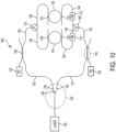
- Figure 10 is a simplified high-level block diagram of components of an optical gyroscope 600 adapted to detect the degree of spin along, e.g., the z-axis.
- Optical gyroscope 600 is similar to optical gyroscope 200 shown in Figure 3 except that optical gyroscope 600 includes a second phase modulator 172 adapted to introduce, for example, a 90° phase shift to the optical signal delivered to or received from optical ring 120.
- the optical gyroscope shown in Figure 10 does not form part of the invention, but represents subject matter that is useful for understanding the invention.
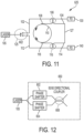
- Figure 11 shows an optical gyroscope 625.
- Optical gyroscope 625 is similar to optical gyroscope 200 except that optical gyroscope 600 includes one optical ring and a waveguide 127 in place of optical ring 120.
- Figure 12 is a simplified high-level block diagram of optical switch 650 corresponding to optical switch 125 shown for example, in Figures 2 and 3 .
- Optical switch 600 is a Mach Zehnder interferometer shown as including, in part, first and second phase shifters 602, 604 and a 50/50 directional coupler 608.
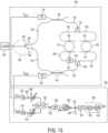
- Figures 13 is a simplified high-level block diagram of components of an optical gyroscope 700 together with the control circuitry 750 (in a manner similar to combined Figures 3 and 6 ) adapted to detect the degree of spin about, e.g., the z-axis.
- signal P out1 generated by photodetector 130 is delivered to trans-impedance amplifier 135 during the first half of each period 0 ⁇ t ⁇ T 2 and signal P out2 generated by photodetector 140 is delivered to trans-impedance amplifier 145 during the second half of each period T 2 ⁇ t ⁇ T .
- Bypass capacitor 302 delivers the output of trans-impedance amplifier 135 to variable gain amplifier 304 and bypass capacitor 312 delivers the output of trans-impedance amplifier 145 to variable gain amplifier 314.
- Electronic switch 752 operates to deliver the output of variable gain amplifier 304 to resistor 326 during the first half of each period 0 ⁇ t ⁇ T 2 and to deliver the output of variable gain amplifier 314 to resistor 326 during the second half of each period T 2 ⁇ t ⁇ T .
- Bandpass filter 328, amplifier 330, mixer 322, low-pass filter 33 and controller 350 operate in the same manner as described above with respect to Figure 6 .
- Signal S out is the read-out of controller 350 showing the degree of rotation about any of the axis.
- electronic switch 752 operates to deliver signal P out1 generated by photodetector 130 to trans-impedance amplifier 135 during the first half of each period 0 ⁇ t ⁇ T 2 and to deliver signal P out2 generated by photodetector 140 to trans-impedance amplifier 145 during the second half of each period T 2 ⁇ t ⁇ T
- Figures 14 is a simplified high-level block diagram of components of an optical gyroscope 800 together with the control circuitry 850 adapted to detect the degree of spin along, e.g., the z-axis.
- phase modulator 170 is adapted to further modulate, at a modulation frequency f 1 , the phase of the signal received or delivered by optical ring 110.
- phase modulator 170 modulates this, e.g., 90° phase shift by a predefined amount using at a modulation frequency of f 1 .
- Signal P out1 generated by photodetector 130 is delivered to trans-impedance amplifier 135 during the first half of each period 0 ⁇ t ⁇ T 2 and signal P out2 generated by photodetector 140 is delivered to trans-impedance amplifier 145 during the second half of each T 2 ⁇ t ⁇ T .
- control circuitry 850 operate in the same manner as described above with respect to Figure 6 except that control circuitry 850 generates an in-phase signal I and a quadrature phase signal Q using a local oscillator (LO) signal 329 that operates at frequency (f 0 +2f 1 ),
- LO local oscillator
- the output signals of low-pass filters 334 and 338 are delivered to controller 350 which generates readout signal S out showing the degree of rotation about any of the axis.
Landscapes
- Physics & Mathematics (AREA)
- Engineering & Computer Science (AREA)
- Electromagnetism (AREA)
- Power Engineering (AREA)
- General Physics & Mathematics (AREA)
- Radar, Positioning & Navigation (AREA)
- Remote Sensing (AREA)
- Optics & Photonics (AREA)
- Gyroscopes (AREA)
Description
- The present invention relates to a gyroscope, and more particularly to an optical gyroscope.
- Gyroscopes are used in a variety of devices, such as smartphones, cars, aircrafts and the like for navigation. As is known, a tradeoff exists between the accuracy of a gyroscope and its size. For example, ring laser gyroscopes or fiber optic gyroscopes with relatively high accuracy are expensive and bulky. Micro electro-mechanical systems (MEMS) based gyroscopes are relatively small but lack precision.
- Conventional benchtop laser-based gyroscopes require high precision alignment, clean medium and a high-quality laser source to detect small phase shift (due to Sagnac effect) and to minimize noise.
-
US Patent No. 4,658,401 , describes a passive ring resonator laser gyro in which the clockwise and counterclockwise beams do not coexist in the resonator. The laser gyro employs thin film technology. In particular, the preferred laser is a gallium aluminum arsenide laser. Light from the laser is phase-modulated by means of a thin film electro-optic modulator comprising a channel waveguide disposed on an electrically active material and flanked by electrodes for modulating the phase of light from the laser. An electro-optic switch is provided for switching light from the laser to inject alternatingly clockwise and counterclockwise beams into the resonator. The resulting gyro is compact and simply implemented into an integrated, thin film package. Because the clockwise and counterclockwise beams do not coexist in the resonator, various beam interaction effects such as beats, backscatter and feedback into the laser are eliminated. - An optical gyroscope, in accordance with a first aspect of the present invention, includes an optical switch adapted to deliver a laser beam to a first path during a first half of a period and to a second path during a second half of the period, a first optical ring configured to deliver a first portion of the beam received from the first path in a clockwise direction during the first half of the period, and further to deliver a first portion of the beam received from the second path in a counter clockwise direction during the second half of the period, a second optical ring configured to deliver a second portion of the beam received from the first path in a counter clockwise direction during the first half of the period, and further to deliver a second portion of the beam received from the second path in a clockwise direction during the second half of the period, a first photodetector adapted to receive the beams delivered by the first and second optical rings during the first half of the period, a second photodetector adapted to receive the beams delivered by the first and second optical rings during the second half of the period, a first trans-impedance amplifier adapted to amplify the output signal of the first photodetector by a first amplification value, a second trans-impedance amplifier adapted to amplify the output signal of the second photodetector by a second amplification value, a first phase modulator adapted to delay a beam received or delivered by the first optical ring by a first predefined phase value, and a signal combiner adapted to generate a first signal representative of a combined outputs of the first and second trans-impedence amplifiers. In one embodiment, the first predefined phase value is a 90° phase value.
- In some embodiments, the optical gyroscope further includes a bandpass filter adapter to filter the first signal. In some embodiments, the optical gyroscope further includes a mixer adapted to downconvert a frequency of the filtered first signal to generate a baseband signal. In some embodiments, the optical gyroscope further includes a controller adapted to convert the baseband signal to a digital signal, and generate a signal representative of a degree of rotation of the optical gyroscope about an axis in response to the digital signal.
- In one embodiment, the first and second optical rings are ring resonators. In one embodiment, each of the first and second ring resonators further includes, in part, one or more heating elements adapted to tune the resonator. In one embodiment, the heating elements are resistive heating elements integrated with the first and second ring resonators. In one embodiment, the signal combiner is adapted to add output signals of the first and second trans-impedance amplifiers. In one embodiment, the optical switch includes a Mach Zehnder interferometer.
- In one embodiment, the optical gyroscope further includes a second phase modulator adapted to delay a signal received or delivered by the second optical ring by a second predefined phase value. In one embodiment, the second phase value is a 90° phase value.
- A method of determining a degree of orientation about an axis, in accordance with a second aspect of the present invention, includes delivering a laser beam to a first path during a first half of a period and to a second path during a second half of the period, delivering a first portion of the beam received from the first path to a first optical ring in a clockwise direction during the first half of the period, delivering a first portion of the beam received from the second path to the first optical ring in a counter clockwise direction during the second half of the period, delivering a second portion of the beam received from the first path to a second optical ring in a counter clockwise direction during the first half of the period, delivering a second portion of the beam received from the second path to the second optical ring in a clockwise direction during the second half of the period, detecting the beams delivered by the first and second optical rings during the first half of the period to generate a first signal, detecting the beams delivered by the first and second optical rings during the second half of the period to generate a second signal, and combining the first and second signals to determine a degree of rotation about the axis, amplifying the first signal by a first amplification value to generate a first amplified signal, amplifying the second signal by a second amplification value to generate a second amplified signal, delaying a beam received or delivered by the first optical ring by a first predefined phase value, and combining the first and second amplified signals to generate a combined signal. In one embodiment, the first predefined phase value is a 90° phase value.
- In one embodiment, the method further includes filtering the combined signal to generate a filtered signal. In one embodiment, the method further includes downconverting the frequency of the filtered signal to generate a baseband signal. In one embodiment, the method further includes converting the baseband signal to a digital signal, and generating a value representative of a degree of rotation of the optical gyroscope about an axis in response to the digital signal.
- In one embodiment, the first and second optical rings are ring resonators. In one embodiment, the method further includes tuning the first and second ring resonators by applying heat. In one embodiment, combining of the first and second amplified signals includes, adding the first and second amplified signals to another signal. In one embodiment, the method further includes delaying a beam received or delivered by the second optical ring by a second predefined phase value. In one embodiment, the second predefined phase value is a 90° phase value.
- The optical gyroscope is an optical gyroscope including first and second optical paths formed using optical waveguides in a semiconductor substrate, a coherent laser source generating two optical signals traveling in the first optical path in one direction and in the second optical path in a second direction opposite the first direction, and a photodetector adapted to receive the beams delivered by the first and second optical paths.
- The optical waveguides are optical rings. The optical rings may bearing resonators.
- The optical gyroscope includes a switch configured to switch between the outputs of the first and second photodetectors. The optical gyroscope may further include, in part, a heater adapted to heat the ring resonator. The optical gyroscope includes a phase modulator adapted to modulate a phase of the beam delivered to or received from the ring resonator.
-
-
Figure 1A shows an optical ring in a stationary state and disposed in a gyroscope, as known in the prior art. -
Figure 1B shows the optical ring ofFigure 1 after rotating along the z-axis and in a counter clock-wise direction, as shown in the prior art. -
Figure 2 is a simplified high-level block diagram of components of an optical gyroscope adapted to detect the amount of spin or rotation along an axis. -
Figure 3 is a simplified high-level block diagram of components of an optical gyroscope adapted to detect the amount of spin along an axis. -
Figure 4 is a simplified schematic block diagram of circuitry adapted to combine the outputs of the photo detectors of the optical gyroscopes shown inFigure 2 or3 . -
Figure 5 is a computer simulation showing the gain ratio in dB as a function of the number of rotations per minute. -
Figure 6 is a high-level block diagram of an integrated optical gyroscope. -
Figure 7 shows plots of measured output powers in dB as a function of wavelength of the laser beam for two different optical rings fabricated in vicinity of one another. -
Figure 8 shows plots of measured output powers in dB as a function of wavelength for the same optical ring. -
Figure 9A is a simplified high-level block diagram of components of an optical gyroscope adapted to detect the amount of spin or rotation along an axis. -
Figure 9B is a simplified high-level block diagram of components of an optical gyroscope adapted to detect the amount of spin or rotation along an axis. -
Figure 9C is a simplified high-level block diagram of components of an optical gyroscope adapted to detect the amount of spin or rotation along an axis. -
Figure 10 is a simplified high-level block diagram of components of an optical gyroscope adapted to detect the amount of spin or rotation along an axis. The optical gyroscope shown inFigure 10 does not form part of the invention, but represents subject matter that is useful for understanding the invention. -
Figure 11 is a simplified high-level block diagram of components of an optical gyroscope adapted to detect the amount of spin or rotation along an axis. -
Figure 12 is a simplified high-level block diagram of the optical switch used in optical gyroscopes ofFigures 2 and3 . -
Figures 13 is a simplified high-level block diagram of components of an optical gyroscope adapted to detect the amount of spin or rotation along an axis. -
Figure 14 is a simplified high-level block diagram of components of an optical gyroscope adapted to detect the amount of spin or rotation along an axis. - In accordance with embodiments of the present invention, an integrated optical gyroscope has a high precision, enhanced immunity to noise and is relatively inexpensive to manufacture.
-
Figure 1A shows anoptical ring 10 assumed to be a part of a gyroscope and adapted to be able to spin about the z axis (perpendicular to the plane of the page). Assume that twolaser beams entry point 12 at the same time. Assume further thatbeam 15 is caused to travel in a clockwise direction (CW) andbeam 20 is caused to travel in a counter clockwise direction (CCW). If the force applied to the gyroscope does not causering 10 to rotate about the z-axis (thereby maintainingring 10 in a stationary state) the position Pi ofentry point 12 does not change and therefore bothbeams entry point 12 at the same, as shown inFigure 1A . - Assume, that due to an applied force,
optical ring 10 is caused to rotate about the z-axis and in a CW direction, as shown inFigure 1B , thereby causing a change in position ofentry point 12 from P1 to P2. This causesbeam 15 to travel a longer distance to reach position P2 than it doesbeam 20. The extra distance traveled bybeam 15 relative tobeam 20 causes a time difference Δt defined by the following expression:
- In equation (1), R, ω and A respectively represent the radius, angular velocity and area of
optical ring 10, and c represents the speed of light. By measuring the time differenceΔt, the angular velocity ω and hence the degree of orientation about the z- axis is determined. Although not shown, it is understood that a gyroscope has three such rings each adapted to rotate about one of the x, y and z axes. - Conventional optical gyroscopes suffer from a number of sources of noise, such as, for example, (i) thermal noise (thermal fluctuations) inside the waveguide or fiber thus inducing phase shift, (ii) fabrication mismatches, (iii) laser phase noise; and (iv) mode conversion inside the waveguide or fiber. An optical gyroscope, in accordance with embodiments of the present invention, minimizes the above sources of noise.
-
Figure 2 is a simplified high-level block diagram of components of anoptical gyroscope 100 adapted to detect the amount of spin or rotation about, e.g., the z-axis (perpendicular to the plane of the page). Although not shown, it is understood thatoptical gyroscope 100 also includes similar components adapted to detect the amount of rotations about both x and y axes. - The, e.g., z-axis components of
optical ring 100 are shown as including an optical switch125, first and secondoptical paths optical rings directional couplers second photodetectors - The laser beam supplied by
laser source 105 is delivered tooptical switch 125 which has a switching frequency of f0 defined by the period
optical switch 125 is placed inposition 190 so as to deliver the laser beam to firstoptical path 102 which is subsequently detected byphotodetector 140. During a second half of each such period,optical switch 125 is placed inposition 192 so as to deliver the laser beam to secondoptical path 112 which is subsequently detected byphotodetector 130. - The laser beam in path 102 (received during the first half of each period T) is delivered to
optical ring 110 bydirectional couplers optical ring 120 bydirectional couplers optical ring 110 travels in a counter clock-wise direction and received atphotodetector 140 viadirectional couplers optical ring 120 travels in a clock-wise direction and received atphotodetector 140 viadirectional couplers - The laser beam in path 112 (received during the second half of each period T) is delivered to
optical ring 110 bydirectional couplers optical ring 120 bydirectional couplers optical ring 110 travels in a clock-wise direction and received atphotodetector 130 viadirectional couplers optical ring 120 travels in a counter clock-wise direction and received atphotodetector 130 viadirectional couplers - When the direction of the coherent laser beam is switched between
paths photodetectors photodetectors optical switch 125 is selected to be relatively high, noise contributions caused, for example, by phase shifts induced by thermal fluctuations (which are in the kHz range) as well as other non-idealities are canceled out. Moreover, because each spin axis of an optical gyroscope includes a pair of rings each enabling the beam to travel in one direction only, back reflections of the beam due to non-ideal characteristics of the waveguides (or fiber) that is common in conventional gyroscopes are inhibited. -
Figure 3 is a simplified high-level block diagram of components of anoptical gyroscope 200 adapted to detect the amount of spin or rotation sbout, e.g., the z-axis (perpendicular to the plane of the page). Although not shown, it is understood thatoptical gyroscope 200 also includes similar components adapted to detect the amount of rotations about both x and y axes. -
Optical gyroscope 200 is similar tooptical gyroscope 100 except thatoptical gyroscope 200 includes aphase modulator 170, and first and second beam splitters/combiners (Y-junction) 160,170.Phase modulator 170 is adapted to introduce, for example, 90° phase shift to the optical signal delivered to or received fromoptical ring 110. - The laser beam supplied by
laser source 105 is delivered tooptical switch 125 which has a switching frequency of f0 defined by the period
optical switch 125 is placed inposition 190 so as to deliver the laser beam to firstoptical path 102, which is subsequently received and detected byphotodetector 140. During a second half of each such period,optical switch 125 is placed inposition 192 so as to deliver the laser beam to secondoptical path 112, which is subsequently received and detected byphotodetector 130. - The optical beam supplied to
path 142 frompath 112 throughoptical coupler 116 is split at Y-junction 160 into two components. The first component of the beam so split passes throughphase modulator 170 before enteringoptical ring 110 viaoptical coupler 118. The second component of the beam travelling onpath 142 is delivered tooptical ring 120 viaoptical coupler 114. The beam traveling inring 110 is delivered topath 156 viaoptical coupler 108. Similarly, the beam traveling inring 120 is delivered topath 158 viaoptical coupler 104. The beams inpaths junction 170 and received byphotodiode 130 frompath 152 viacoupler 106. - Similarly, the optical beam supplied to
path 152 frompath 102 throughoptical coupler 106 is split at Y-junction 170 into two components. The first component of the beam so split entersoptical ring 110 viaoptical coupler 108. The second component of the beam travelling inpath 152 is delivered tooptical ring 120 viaoptical coupler 104. The beam traveling inring 110 is delivered to path 180-via coupler 118-and passes throughphase modulator 170 before reaching Y-junction 160. The beam traveling inring 120 is delivered to path 148-via coupler 114 -before reaching Y-junction 160. The beams inpaths junction 160 and received byphotodiode 140 frompath 142 viacoupler 116. - Referring to
Figure 3 , assume thatoptical rings 
switch 195 ofoptical switch 125 is placed inposition 190 to deliver the beam tooptical path 102, the power P out2 detected byphotodetector 140 may be defined as:
- In equation (2), P out2 represents the amount of optical power detected by photo detector 140, Pin is the power supplied by laser source 105, K1 represents the fraction of the laser power delivered to path 102 by switch 125 (which ideally is equal to 1), α 1 represents the coupling coefficient of optical coupler 106 (which ideally is equal to 0.5), α 2 represents the coupling coefficient of optical coupler 116, X 1 and X 11 represent the attenuation coefficients of ring resonators 110 and 120 respectively,


- Given the above definitions, it is seen that:


- During the first half of each period


- During the second half of each
period 
switch 195 ofoptical switch 125 is inposition 192 to deliver the beam tooptical path 112, power P out2 detected byphotodetector 140 may be defined as:
- In equation (4), K 2 represents the fraction of the laser power delivered to
path 102 by switch 125 (which ideally is equal to 1). During the second half of each period, power P out1 detected byphotodetector 130 may be defined as:
- Assuming ideal conditions in which case both K1 and K2 would be equal to 1, during the first period P out1 would be zero and during the second period P out2 would be zero. Therefore, under such conditions, signal P out1 of the first period and signal P out2 of the second period would not contribute to the combined signals received by
photo detectors - To account for non-ideal characteristics when detecting signal Δϕsag , the output signal of each of
photodetectors Figure 4 shows a simplified schematic block diagram ofphotodiodes 130 and 140 (seeFigure 3 ) whose outputs are amplified by trans-impedance amplifiers impedance amplifiers combiner 155 to generate signal Out representative of the degree of rotation along, e.g., the z-axis, as described above. In one embodiment,combiner 155 adds the signal Δϕsag representative of the degree of rotation to a base signal during a first half period of each cycle, and subtracts signal Δϕsag from the base signal during a second half period of each cycle. - Accordingly, during the first half of each period


- Likewise, during the second half of each
period 

- In simplified equations (6) and (7), parametersγ 1, k 1 , γ 2, k2,


- In deriving equation (8) it is assumed that

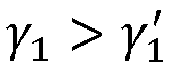
switch 195 is placed inposition 190, more than 50% of the laser beam power is delivered topath 102, and whenswitch 195 is placed inposition 192, more than 50% of the laser beam power is delivered topath 112. -
Figure 5 is a computer simulation showing the gain in dB of
Figure 6 , to more accurately determine Δϕsαg as the RPM of the gyroscope decreases, the higher should be the accuracy with which
-
Figure 6 is a high-level block diagram of an integratedoptical gyroscope system 400.Gyroscope system 400 is adapted to detect the degree of rotations along x, y and z directions and is shown as including in, part, anintegrated photonics chip 300.Integrated photonics chip 300 may include thegyroscopes Figures 2 and3 respectively. Output current signals P1 and P2 generated by, e.g.,photodetectors Figures 2 and3 , are amplified by trans-impedance amplifiers impedance amplifiers 135 is further amplified byvoltage amplifier 304 after passing throughbypass capacitor 302 which is adapted to block DC components of the signal. Similarly, the output voltage of trans-impedance amplifiers 145 is further amplified byvoltage amplifier 314 after passing throughbypass capacitor 312. -
Variable resistors amplifier 324 andfeedback resistor 322 are adapted to set the relative gain of the voltages Vi (received from resistor 308) and V2 (received from resistor 318) and add the voltages together. For example, iffeedback resistor 322 is selected to have a resistance of 20 KΩ andresistors amplifier 324 will generate an output voltage defined by 20V1+10V2.Resistors pass capacitor 320,amplifier 324 andresistor 322 collectively show one exemplary embodiment ofcombiner 155 shown inFigure 4 .Bandpass filter 328 is adapted to filter out signal components whose frequencies fall within a selected range.Resistor 326 is adapted to match the output impedance ofamplifier 324 to the input impedance ofbandpass filter 328. - The output signal of the
bandpass filter 328 is further amplified byamplifier 330 and its frequency is downconverted to a baseband signal bymixer 332 in response to local oscillator (LO)signal 329. The output ofmixer 322 is filtered by low-pass filter 334.Micro-controller 350, shown as including an analog-to-digital converter 336 and adigital signal processor 340, converts the output of low-pass filter 334 to a read-out value Sout representative of the degree of rotation of the gyroscope about any of the three axes. -
Figure 7 showsplots Figure 7 , the peaks of the output powers occur at different wavelengths or frequencies for the two optical rings indicating a mismatch between the characteristics of two optical rings even when they are formed near one another. -
Figure 8 showsplots Figure 8 , the peaks ofplots - In some embodiment,
optical rings -
Figures 9A is a simplified high-level block diagram of components of anoptical gyroscope 500 adapted to detect the degree of spin along, e.g., the z-axis.Optical gyroscope 500 is similar tooptical gyroscope 100 ofFigure 2 except thatoptical gyroscope 500 includesresistive heating elements 510 positioned adjacent portions of the periphery and within inner areas ofrings -
Figures 9B is a simplified high-level block diagram of components of anoptical gyroscope 525 adapted to detect the degree of spin along, e.g., the z-axis.Optical gyroscope 500 is similar tooptical gyroscope 100 ofFigure 2 except thatoptical gyroscope 500 includesresistive heating elements 510 positioned adjacent portions of the periphery and within outer areas ofrings -
Figures 9C is a simplified high-level block diagram of components of anoptical gyroscope 550 adapted to detect the degree of spin along, e.g., the z-axis.Optical gyroscope 550 is similar tooptical gyroscope 100 ofFigure 2 except thatoptical gyroscope 550 includesresistive heaters 510 that partly overlap portions of therings -
Figure 10 is a simplified high-level block diagram of components of anoptical gyroscope 600 adapted to detect the degree of spin along, e.g., the z-axis.Optical gyroscope 600 is similar tooptical gyroscope 200 shown inFigure 3 except thatoptical gyroscope 600 includes asecond phase modulator 172 adapted to introduce, for example, a 90° phase shift to the optical signal delivered to or received fromoptical ring 120. The optical gyroscope shown inFigure 10 does not form part of the invention, but represents subject matter that is useful for understanding the invention. -
Figure 11 shows anoptical gyroscope 625.Optical gyroscope 625 is similar tooptical gyroscope 200 except thatoptical gyroscope 600 includes one optical ring and awaveguide 127 in place ofoptical ring 120. -
Figure 12 is a simplified high-level block diagram ofoptical switch 650 corresponding tooptical switch 125 shown for example, inFigures 2 and3 .Optical switch 600 is a Mach Zehnder interferometer shown as including, in part, first andsecond phase shifters directional coupler 608. -
Figures 13 is a simplified high-level block diagram of components of anoptical gyroscope 700 together with the control circuitry 750 (in a manner similar to combinedFigures 3 and6 ) adapted to detect the degree of spin about, e.g., the z-axis. In the embodiment shown inFigure 13 , signal Pout1 generated byphotodetector 130 is delivered to trans-impedance amplifier 135 during the first half of each period
photodetector 140 is delivered to trans-impedance amplifier 145 during the second half of eachperiod 
Bypass capacitor 302 delivers the output of trans-impedance amplifier 135 tovariable gain amplifier 304 andbypass capacitor 312 delivers the output of trans-impedance amplifier 145 tovariable gain amplifier 314.Electronic switch 752 operates to deliver the output ofvariable gain amplifier 304 toresistor 326 during the first half of each period
variable gain amplifier 314 toresistor 326 during the second half of eachperiod 
- .
Bandpass filter 328,amplifier 330,mixer 322, low-pass filter 33 andcontroller 350 operate in the same manner as described above with respect toFigure 6 . Signal Sout is the read-out ofcontroller 350 showing the degree of rotation about any of the axis.electronic switch 752 operates to deliver signal Pout1 generated byphotodetector 130 to trans-impedance amplifier 135 during the first half of each period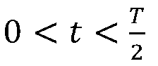
photodetector 140 to trans-impedance amplifier 145 during the second half of eachperiod 
-
Figures 14 is a simplified high-level block diagram of components of anoptical gyroscope 800 together with thecontrol circuitry 850 adapted to detect the degree of spin along, e.g., the z-axis. In the embodiment shown inFigure 14 ,phase modulator 170 is adapted to further modulate, at a modulation frequency f1, the phase of the signal received or delivered byoptical ring 110. For example, in addition to a phase shift of, e.g., 90°,phase modulator 170 modulates this, e.g., 90° phase shift by a predefined amount using at a modulation frequency of f1. Signal Pout1 generated byphotodetector 130 is delivered to trans-impedance amplifier 135 during the first half of each period 0 <
photodetector 140 is delivered to trans-impedance amplifier 145 during the second half of each
control circuitry 850 operate in the same manner as described above with respect toFigure 6 except thatcontrol circuitry 850 generates an in-phase signal I and a quadrature phase signal Q using a local oscillator (LO) signal 329 that operates at frequency (f0+2f1), The output signals of low-pass filters controller 350 which generates readout signal Sout showing the degree of rotation about any of the axis. - The above embodiments are illustrative and not limitative. Other modifications and variations will be apparent to those skilled in the art.
Claims (9)
- An optical gyroscope (100) comprising:an optical switch (125) adapted to deliver a laser beam (105) to a first path (102) during a first half of a period and to a second path (112) during a second half of the period;a first optical ring (110) configured to deliver a first portion of the beam received from the first path (102) in a counter clockwise direction during the first half of the period, and further to deliver a first portion of the beam received from the second path (112) in a clockwise direction during the second half of the period;a second optical ring (120) configured to deliver a second portion of the beam received from the first path (102) in a clockwise direction during the first half of the period, and further to deliver a second portion of the beam received from the second path (112) in a counter clockwise direction during the second half of the period;a first photodetector (130) adapted to receive the beams delivered by the first (110) and second (120) optical rings during the second half of the period;a second photodetector (140) adapted to receive the beams delivered by the first (110) and second (120) optical rings during the first half of the period;a first trans-impedance amplifier (135) adapted to amplify an output signal of the first photodetector (130) by a first amplification value;a second trans-impedance amplifier (145) adapted to amplify an output signal of the second photodetector (140) by a second amplification value;a first phase modulator (170) adapted to delay a beam received or delivered by the first optical ring (110) by a first predefined phase value; anda signal combiner (155) adapted to generate a first signal representative of a combined output of the first (135) and second (145) trans-impedance amplifiers.
- The optical gyroscope of claim 1 wherein said first predefined phase value is a 90° phase value.
- The optical gyroscope of claim 1 wherein said first and second optical rings (110, 120) are ring resonators.
- The optical gyroscope of claim 3 wherein each of the first and second ring resonators comprises one or more heating elements (510) adapted to tune the resonator.
- The optical gyroscope of claim 1 further comprising:
a second phase modulator (172) adapted to delay a signal received or delivered by the second optical ring by a second predefined phase value. - A method of determining a degree of orientation about an axis, the method comprising:delivering a laser beam (105) to a first path (102) during a first half of a period and to a second path (112) during a second half of the period;delivering a first portion of the beam received from the first path (102) to a first optical ring (110) in a counter clockwise direction during the first half of the period;delivering a first portion of the beam received from the second path (112) to the first optical ring (110) in a clockwise direction during the second half of the period;delivering a second portion of the beam received from the first path (102) to a second optical ring (120) in a clockwise direction during the first half of the period;delivering a second portion of the beam received from the second path (112) to the second optical ring (120) in a counter clockwise direction during the second half of the period;detecting the beams delivered by the first and second optical rings (110, 120) during the first half of the period to generate a first signal;detecting the beams delivered by the first and second optical rings (110, 120) during the second half of the period to generate a second signal;amplifying (135) the first signal by a first amplification value to generate a first amplified signal;amplifying (145) the second signal by a second amplification value to generate a second amplified signal;delaying a beam received or delivered by the first optical ring (110) by a first predefined phase value; andcombining the first and second amplified signals to generate a combined signal.
- The method of claim of claim 6 wherein said first predefined phase value is a 90° phase value.
- The method of claim 6 wherein said first and second optical rings (110, 120) are ring resonators.
- The method of claim 8 further comprising:
tuning the first and second ring resonators by applying heat.
Applications Claiming Priority (2)
| Application Number | Priority Date | Filing Date | Title |
|---|---|---|---|
| US201762512619P | 2017-05-30 | 2017-05-30 | |
| PCT/US2018/035207 WO2018222768A1 (en) | 2017-05-30 | 2018-05-30 | Integrated optical gyroscope with noise cancellation |
Publications (3)
| Publication Number | Publication Date |
|---|---|
| EP3631361A1 EP3631361A1 (en) | 2020-04-08 |
| EP3631361A4 EP3631361A4 (en) | 2021-02-24 |
| EP3631361B1 true EP3631361B1 (en) | 2025-01-01 |
Family
ID=64455566
Family Applications (1)
| Application Number | Title | Priority Date | Filing Date |
|---|---|---|---|
| EP18810298.2A Active EP3631361B1 (en) | 2017-05-30 | 2018-05-30 | Integrated optical gyroscope with noise cancellation |
Country Status (5)
| Country | Link |
|---|---|
| US (2) | US10495462B2 (en) |
| EP (1) | EP3631361B1 (en) |
| JP (1) | JP7253493B2 (en) |
| CN (1) | CN110651167B (en) |
| WO (1) | WO2018222768A1 (en) |
Families Citing this family (10)
| Publication number | Priority date | Publication date | Assignee | Title |
|---|---|---|---|---|
| US10578438B2 (en) * | 2016-02-12 | 2020-03-03 | Agency For Science, Technology And Research | Optical gyroscope, electro-optic system, and methods of forming the same |
| JP7253493B2 (en) | 2017-05-30 | 2023-04-06 | カリフォルニア インスティチュート オブ テクノロジー | Integrated optical gyroscope with noise rejection |
| US11405125B2 (en) * | 2018-07-12 | 2022-08-02 | Ayar Labs, Inc. | TORminator system and associated methods |
| US10948296B2 (en) | 2018-08-02 | 2021-03-16 | California Institute Of Technology | Interlaced spiral optical gyroscope |
| US10823571B1 (en) * | 2019-07-31 | 2020-11-03 | Honeywell International Inc. | Switching SBS gyro with fixed pump separation |
| US11656081B2 (en) | 2019-10-18 | 2023-05-23 | Anello Photonics, Inc. | Integrated photonics optical gyroscopes optimized for autonomous terrestrial and aerial vehicles |
| US10989535B1 (en) * | 2020-01-31 | 2021-04-27 | Northrop Grumman Systems Corporation | Calibration circuit to mitigate fiber-optic gyroscope (FOG) bias error |
| DE102020210079B3 (en) | 2020-08-10 | 2021-08-19 | Conti Temic Microelectronic Gmbh | Radar method and radar system with high range resolution with little signal processing effort |
| CN117128945B (en) * | 2023-10-20 | 2023-12-26 | 中北大学 | Super-sensitive angular velocity sensor based on singular surface and measuring method |
| US20250321102A1 (en) * | 2024-04-12 | 2025-10-16 | Honeywell International Inc. | Techniques for increasing round trip path length through an optical resonator coil without substantially increasing optical resonator coil size |
Family Cites Families (41)
| Publication number | Priority date | Publication date | Assignee | Title |
|---|---|---|---|---|
| US6458A (en) | 1849-05-22 | Boring and mortising machine | ||
| US401A (en) | 1837-09-21 | John bouis | ||
| JPS6085312A (en) * | 1983-10-17 | 1985-05-14 | Hitachi Ltd | Solid state interferometer |
| US4658401A (en) * | 1984-03-15 | 1987-04-14 | Northrop Corporation | Thin film passive ring resonator laser gyro |
| DE3426867A1 (en) * | 1984-07-20 | 1986-01-30 | LITEF Litton Technische Werke der Hellige GmbH, 7800 Freiburg | METHOD AND DEVICE FOR MEASURING THE TURN RATE USING THE SAGNAC EFFECT |
| JPS6247516A (en) * | 1985-08-23 | 1987-03-02 | ノ−スロツプ・コ−ポレ−シヨン | Thin-film laser gyro |
| GB8603375D0 (en) * | 1986-02-11 | 1986-03-19 | Jackson D A | Fibre optic data ring & current detector |
| US5237387A (en) * | 1989-09-07 | 1993-08-17 | Honeywell Inc. | Dual serrodyne resonator fiber optic gyroscope |
| JPH03142317A (en) * | 1989-10-27 | 1991-06-18 | Meitec Corp | Optical gyro |
| US5394242A (en) * | 1989-12-15 | 1995-02-28 | The Charles Stark Draper Laboratory, Inc. | Fiber optic resonant ring sensor and source |
| CA2036137A1 (en) * | 1990-05-15 | 1991-11-16 | Richard B. Dyott | Compound fiber-optic gyroscope using frequency discrimination |
| US5157461A (en) * | 1990-06-14 | 1992-10-20 | Smiths Industries Aerospace & Defense Systems Inc. | Interface configuration for rate sensor apparatus |
| JPH04178520A (en) * | 1990-11-14 | 1992-06-25 | Tamagawa Seiki Co Ltd | Optical fiber gyro |
| DE4135132A1 (en) | 1991-10-24 | 1993-04-29 | Bodenseewerk Geraetetech | SENSOR USING A NON-RECIPROCIAL OPTICAL EFFECT |
| JP2963612B2 (en) * | 1994-03-30 | 1999-10-18 | 日立電線株式会社 | Optical rotation angular velocity sensor |
| FR2734632B1 (en) * | 1995-05-24 | 1997-07-25 | Sextant Avionique | GYROMETRIC DETECTION METHOD AND SAMPLE OPTICAL GYROMETER FOR CARRYING OUT SAID METHOD |
| KR100208773B1 (en) * | 1997-07-05 | 1999-07-15 | 윤덕용 | Pulsed ring laser gyroscope with traveling direction |
| US6259089B1 (en) * | 1998-05-15 | 2001-07-10 | Rice Systems, Inc. | Integrated optics rotation sensor |
| US6587205B2 (en) * | 2000-07-28 | 2003-07-01 | Litton Systems, Inc | Integrated optic gyroscope and method of fabrication |
| CN1264000C (en) * | 2002-04-03 | 2006-07-12 | 中国科学技术大学 | Self-injection locking fibre-optical laser circulator |
| CN1277102C (en) * | 2002-12-06 | 2006-09-27 | 北京大学 | Double Ring Resonant Fiber Optic Gyroscope |
| US7305153B2 (en) * | 2005-06-21 | 2007-12-04 | Litton Systems, Inc. | Multi wavelength sensor array |
| US20080013094A1 (en) * | 2006-07-14 | 2008-01-17 | Honeywell International Inc. | Semiconductor substrate for interferometer fiber optic gyroscopes |
| US20080291459A1 (en) * | 2007-05-22 | 2008-11-27 | Litton Systems, Inc. | Fiber optic gyroscope with integrated light source |
| US8098380B2 (en) * | 2009-07-21 | 2012-01-17 | Honeywell International Inc. | Resonator fiber optic gyroscope (RFOG) with reduced bias error from high order spatial modes |
| CN101900556A (en) * | 2010-07-15 | 2010-12-01 | 哈尔滨工程大学 | Double Loop Brillouin Fiber Optic Gyroscope |
| US8274659B2 (en) * | 2010-08-30 | 2012-09-25 | Honeywell International Inc. | Resonator fiber optic gyroscopes with reduced rotation rate instability from back reflections |
| US9306363B1 (en) * | 2010-10-05 | 2016-04-05 | Stc.Unm | Active bidirectional mode-locked lasers and applications to accurate measurements in navigation systems |
| US8823946B1 (en) * | 2011-06-13 | 2014-09-02 | Emcore Corporation | Multi-axis fiber optic gyroscope with single light source |
| US9823075B2 (en) * | 2013-01-10 | 2017-11-21 | Xiaotian Steve Yao | Non-interferometric optical gyroscope based on polarization sensing |
| US9857176B2 (en) * | 2013-06-20 | 2018-01-02 | Tubitak (Turkiye Bilimsel Ve Teknolojik Arastirma Kurumu) | Dynamically monitoring the instantaneous zero rotation rate voltage of interferometric fiber optic gyroscope (IFOG) |
| CN103389084B (en) * | 2013-07-19 | 2015-09-30 | 哈尔滨工程大学 | Based on the resonance type optical fiber gyro of two coupled fiber ring resonator coherence effect |
| CA2930856A1 (en) * | 2013-12-20 | 2015-06-25 | Halliburton Energy Services, Inc. | Downhole em sensing using sagnac interferometer for wellbore monitoring |
| CN104613954B (en) * | 2015-01-27 | 2017-04-12 | 浙江大学 | Single-light source double-peak fiber optic gyro |
| WO2016127321A1 (en) * | 2015-02-10 | 2016-08-18 | 深圳大学 | Ring laser sensor |
| US9389081B1 (en) * | 2015-04-17 | 2016-07-12 | Honeywell International Inc. | Three-laser resonator fiber optic gyroscope with enhanced frequency reference cavity |
| US9459101B1 (en) * | 2015-06-15 | 2016-10-04 | Honeywell International Inc. | Systems and methods for fiber optic gyroscopes utilizing reference ring resonators |
| CN105466411B (en) * | 2015-12-30 | 2018-09-07 | 浙江大学 | Four axis fibre optic gyroscopes and its north finding method |
| US10578438B2 (en) * | 2016-02-12 | 2020-03-03 | Agency For Science, Technology And Research | Optical gyroscope, electro-optic system, and methods of forming the same |
| CN105973220A (en) * | 2016-05-05 | 2016-09-28 | 浙江大学 | Secondary frequency signal detection technology-based resonant fiber optic gyroscope light source intensity modulation noise inhibition method and device |
| JP7253493B2 (en) | 2017-05-30 | 2023-04-06 | カリフォルニア インスティチュート オブ テクノロジー | Integrated optical gyroscope with noise rejection |
-
2018
- 2018-05-30 JP JP2019545935A patent/JP7253493B2/en active Active
- 2018-05-30 WO PCT/US2018/035207 patent/WO2018222768A1/en not_active Ceased
- 2018-05-30 EP EP18810298.2A patent/EP3631361B1/en active Active
- 2018-05-30 US US15/993,525 patent/US10495462B2/en active Active
- 2018-05-30 CN CN201880032107.0A patent/CN110651167B/en active Active
-
2019
- 2019-12-03 US US16/701,810 patent/US11131546B2/en active Active
Also Published As
| Publication number | Publication date |
|---|---|
| US20200278207A1 (en) | 2020-09-03 |
| CN110651167B (en) | 2023-10-31 |
| JP7253493B2 (en) | 2023-04-06 |
| EP3631361A1 (en) | 2020-04-08 |
| US11131546B2 (en) | 2021-09-28 |
| JP2020522677A (en) | 2020-07-30 |
| CN110651167A (en) | 2020-01-03 |
| US10495462B2 (en) | 2019-12-03 |
| EP3631361A4 (en) | 2021-02-24 |
| WO2018222768A1 (en) | 2018-12-06 |
| US20180356229A1 (en) | 2018-12-13 |
Similar Documents
| Publication | Publication Date | Title |
|---|---|---|
| EP3631361B1 (en) | Integrated optical gyroscope with noise cancellation | |
| US11293757B2 (en) | Non-interferometric optical gyroscope based on polarization sensing and implementations of closed loop control allowing for slow phase modulation | |
| US9459101B1 (en) | Systems and methods for fiber optic gyroscopes utilizing reference ring resonators | |
| KR102551725B1 (en) | Photon Integrated Circuits for Interferometric Fiber Optic Gyroscopes (IFOGs) | |
| US10948296B2 (en) | Interlaced spiral optical gyroscope | |
| US8446589B2 (en) | Residual intensity modulation (RIM) control loop in a resonator fiber-optic gyroscope (RFOG) | |
| US8908187B2 (en) | System and method for reducing errors in a resonator fiber optic gyroscope | |
| EP2221579B1 (en) | RFOG-modulation error correction | |
| US9001336B1 (en) | Methods and apparatus of tracking/locking resonator free spectral range and its application in resonator fiber optic gyroscope | |
| US8830479B2 (en) | RFOG with optical heterodyning for optical signal discrimination | |
| JP2863009B2 (en) | Reduction of Kerr effect error of resonator optical fiber gyroscope | |
| US20120050745A1 (en) | Resonator fiber optic gyroscopes with reduced rotation rate instability from back reflections | |
| JPS6060513A (en) | Optical-fiber gyroscope and method of changing phase of said gyroscope into zero | |
| US20150098089A1 (en) | Optical passive resonator gyro with three beams | |
| US7333209B2 (en) | Fiber optic gyroscope asynchronous demodulation | |
| EP0532699B1 (en) | Eigenfrequency phase shift control loop | |
| EP3617648B1 (en) | Hyperbolic modulation offset error reducer for an rfog | |
| GB2028496A (en) | Interferometer gyro | |
| US12123718B1 (en) | Mitigating bias instabilities in optical gyroscopes | |
| Armenise et al. | Out-of-resonance measurement scheme for ring resonator gyroscopes |
Legal Events
| Date | Code | Title | Description |
|---|---|---|---|
| STAA | Information on the status of an ep patent application or granted ep patent |
Free format text: STATUS: THE INTERNATIONAL PUBLICATION HAS BEEN MADE |
|
| PUAI | Public reference made under article 153(3) epc to a published international application that has entered the european phase |
Free format text: ORIGINAL CODE: 0009012 |
|
| STAA | Information on the status of an ep patent application or granted ep patent |
Free format text: STATUS: REQUEST FOR EXAMINATION WAS MADE |
|
| 17P | Request for examination filed |
Effective date: 20191224 |
|
| AK | Designated contracting states |
Kind code of ref document: A1 Designated state(s): AL AT BE BG CH CY CZ DE DK EE ES FI FR GB GR HR HU IE IS IT LI LT LU LV MC MK MT NL NO PL PT RO RS SE SI SK SM TR |
|
| AX | Request for extension of the european patent |
Extension state: BA ME |
|
| RIN1 | Information on inventor provided before grant (corrected) |
Inventor name: HAJIMIRI, SEYED ALI Inventor name: PORSANDEH KHIAL, PARHAM |
|
| DAV | Request for validation of the european patent (deleted) | ||
| DAX | Request for extension of the european patent (deleted) | ||
| A4 | Supplementary search report drawn up and despatched |
Effective date: 20210122 |
|
| RIC1 | Information provided on ipc code assigned before grant |
Ipc: G01C 19/72 20060101ALI20210118BHEP Ipc: G02F 1/21 20060101ALI20210118BHEP Ipc: G01C 19/64 20060101AFI20210118BHEP Ipc: G01C 19/66 20060101ALI20210118BHEP |
|
| STAA | Information on the status of an ep patent application or granted ep patent |
Free format text: STATUS: EXAMINATION IS IN PROGRESS |
|
| 17Q | First examination report despatched |
Effective date: 20220906 |
|
| GRAP | Despatch of communication of intention to grant a patent |
Free format text: ORIGINAL CODE: EPIDOSNIGR1 |
|
| STAA | Information on the status of an ep patent application or granted ep patent |
Free format text: STATUS: GRANT OF PATENT IS INTENDED |
|
| INTG | Intention to grant announced |
Effective date: 20240731 |
|
| GRAS | Grant fee paid |
Free format text: ORIGINAL CODE: EPIDOSNIGR3 |
|
| GRAA | (expected) grant |
Free format text: ORIGINAL CODE: 0009210 |
|
| STAA | Information on the status of an ep patent application or granted ep patent |
Free format text: STATUS: THE PATENT HAS BEEN GRANTED |
|
| AK | Designated contracting states |
Kind code of ref document: B1 Designated state(s): AL AT BE BG CH CY CZ DE DK EE ES FI FR GB GR HR HU IE IS IT LI LT LU LV MC MK MT NL NO PL PT RO RS SE SI SK SM TR |
|
| REG | Reference to a national code |
Ref country code: GB Ref legal event code: FG4D |
|
| P01 | Opt-out of the competence of the unified patent court (upc) registered |
Free format text: CASE NUMBER: APP_63366/2024 Effective date: 20241128 |
|
| REG | Reference to a national code |
Ref country code: CH Ref legal event code: EP |
|
| REG | Reference to a national code |
Ref country code: DE Ref legal event code: R096 Ref document number: 602018078158 Country of ref document: DE |
|
| REG | Reference to a national code |
Ref country code: IE Ref legal event code: FG4D |
|
| REG | Reference to a national code |
Ref country code: LT Ref legal event code: MG9D |
|
| REG | Reference to a national code |
Ref country code: NL Ref legal event code: MP Effective date: 20250101 |
|
| REG | Reference to a national code |
Ref country code: AT Ref legal event code: MK05 Ref document number: 1756645 Country of ref document: AT Kind code of ref document: T Effective date: 20250101 |
|
| PG25 | Lapsed in a contracting state [announced via postgrant information from national office to epo] |
Ref country code: NL Free format text: LAPSE BECAUSE OF FAILURE TO SUBMIT A TRANSLATION OF THE DESCRIPTION OR TO PAY THE FEE WITHIN THE PRESCRIBED TIME-LIMIT Effective date: 20250101 |
|
| PG25 | Lapsed in a contracting state [announced via postgrant information from national office to epo] |
Ref country code: FI Free format text: LAPSE BECAUSE OF FAILURE TO SUBMIT A TRANSLATION OF THE DESCRIPTION OR TO PAY THE FEE WITHIN THE PRESCRIBED TIME-LIMIT Effective date: 20250101 |
|
| PG25 | Lapsed in a contracting state [announced via postgrant information from national office to epo] |
Ref country code: PL Free format text: LAPSE BECAUSE OF FAILURE TO SUBMIT A TRANSLATION OF THE DESCRIPTION OR TO PAY THE FEE WITHIN THE PRESCRIBED TIME-LIMIT Effective date: 20250101 |
|
| PGFP | Annual fee paid to national office [announced via postgrant information from national office to epo] |
Ref country code: DE Payment date: 20250529 Year of fee payment: 8 |
|
| PG25 | Lapsed in a contracting state [announced via postgrant information from national office to epo] |
Ref country code: ES Free format text: LAPSE BECAUSE OF FAILURE TO SUBMIT A TRANSLATION OF THE DESCRIPTION OR TO PAY THE FEE WITHIN THE PRESCRIBED TIME-LIMIT Effective date: 20250101 |
|
| PG25 | Lapsed in a contracting state [announced via postgrant information from national office to epo] |
Ref country code: IS Free format text: LAPSE BECAUSE OF FAILURE TO SUBMIT A TRANSLATION OF THE DESCRIPTION OR TO PAY THE FEE WITHIN THE PRESCRIBED TIME-LIMIT Effective date: 20250501 Ref country code: NO Free format text: LAPSE BECAUSE OF FAILURE TO SUBMIT A TRANSLATION OF THE DESCRIPTION OR TO PAY THE FEE WITHIN THE PRESCRIBED TIME-LIMIT Effective date: 20250401 |
|
| PG25 | Lapsed in a contracting state [announced via postgrant information from national office to epo] |
Ref country code: HR Free format text: LAPSE BECAUSE OF FAILURE TO SUBMIT A TRANSLATION OF THE DESCRIPTION OR TO PAY THE FEE WITHIN THE PRESCRIBED TIME-LIMIT Effective date: 20250101 |
|
| PG25 | Lapsed in a contracting state [announced via postgrant information from national office to epo] |
Ref country code: LV Free format text: LAPSE BECAUSE OF FAILURE TO SUBMIT A TRANSLATION OF THE DESCRIPTION OR TO PAY THE FEE WITHIN THE PRESCRIBED TIME-LIMIT Effective date: 20250101 Ref country code: PT Free format text: LAPSE BECAUSE OF FAILURE TO SUBMIT A TRANSLATION OF THE DESCRIPTION OR TO PAY THE FEE WITHIN THE PRESCRIBED TIME-LIMIT Effective date: 20250502 |
|
| PGFP | Annual fee paid to national office [announced via postgrant information from national office to epo] |
Ref country code: FR Payment date: 20250526 Year of fee payment: 8 |
|
| PG25 | Lapsed in a contracting state [announced via postgrant information from national office to epo] |
Ref country code: BG Free format text: LAPSE BECAUSE OF FAILURE TO SUBMIT A TRANSLATION OF THE DESCRIPTION OR TO PAY THE FEE WITHIN THE PRESCRIBED TIME-LIMIT Effective date: 20250101 Ref country code: GR Free format text: LAPSE BECAUSE OF FAILURE TO SUBMIT A TRANSLATION OF THE DESCRIPTION OR TO PAY THE FEE WITHIN THE PRESCRIBED TIME-LIMIT Effective date: 20250402 |
|
| PG25 | Lapsed in a contracting state [announced via postgrant information from national office to epo] |
Ref country code: AT Free format text: LAPSE BECAUSE OF FAILURE TO SUBMIT A TRANSLATION OF THE DESCRIPTION OR TO PAY THE FEE WITHIN THE PRESCRIBED TIME-LIMIT Effective date: 20250101 |
|
| PG25 | Lapsed in a contracting state [announced via postgrant information from national office to epo] |
Ref country code: CZ Free format text: LAPSE BECAUSE OF FAILURE TO SUBMIT A TRANSLATION OF THE DESCRIPTION OR TO PAY THE FEE WITHIN THE PRESCRIBED TIME-LIMIT Effective date: 20250101 |
|
| PG25 | Lapsed in a contracting state [announced via postgrant information from national office to epo] |
Ref country code: SE Free format text: LAPSE BECAUSE OF FAILURE TO SUBMIT A TRANSLATION OF THE DESCRIPTION OR TO PAY THE FEE WITHIN THE PRESCRIBED TIME-LIMIT Effective date: 20250101 |
|
| REG | Reference to a national code |
Ref country code: DE Ref legal event code: R097 Ref document number: 602018078158 Country of ref document: DE |
|
| PG25 | Lapsed in a contracting state [announced via postgrant information from national office to epo] |
Ref country code: SM Free format text: LAPSE BECAUSE OF FAILURE TO SUBMIT A TRANSLATION OF THE DESCRIPTION OR TO PAY THE FEE WITHIN THE PRESCRIBED TIME-LIMIT Effective date: 20250101 |
|
| PG25 | Lapsed in a contracting state [announced via postgrant information from national office to epo] |
Ref country code: DK Free format text: LAPSE BECAUSE OF FAILURE TO SUBMIT A TRANSLATION OF THE DESCRIPTION OR TO PAY THE FEE WITHIN THE PRESCRIBED TIME-LIMIT Effective date: 20250101 |
|
| PG25 | Lapsed in a contracting state [announced via postgrant information from national office to epo] |
Ref country code: IT Free format text: LAPSE BECAUSE OF FAILURE TO SUBMIT A TRANSLATION OF THE DESCRIPTION OR TO PAY THE FEE WITHIN THE PRESCRIBED TIME-LIMIT Effective date: 20250101 |
|
| PG25 | Lapsed in a contracting state [announced via postgrant information from national office to epo] |
Ref country code: EE Free format text: LAPSE BECAUSE OF FAILURE TO SUBMIT A TRANSLATION OF THE DESCRIPTION OR TO PAY THE FEE WITHIN THE PRESCRIBED TIME-LIMIT Effective date: 20250101 |
|
| PG25 | Lapsed in a contracting state [announced via postgrant information from national office to epo] |
Ref country code: RO Free format text: LAPSE BECAUSE OF FAILURE TO SUBMIT A TRANSLATION OF THE DESCRIPTION OR TO PAY THE FEE WITHIN THE PRESCRIBED TIME-LIMIT Effective date: 20250101 |
|
| PG25 | Lapsed in a contracting state [announced via postgrant information from national office to epo] |
Ref country code: SK Free format text: LAPSE BECAUSE OF FAILURE TO SUBMIT A TRANSLATION OF THE DESCRIPTION OR TO PAY THE FEE WITHIN THE PRESCRIBED TIME-LIMIT Effective date: 20250101 |
|
| PLBE | No opposition filed within time limit |
Free format text: ORIGINAL CODE: 0009261 |
|
| STAA | Information on the status of an ep patent application or granted ep patent |
Free format text: STATUS: NO OPPOSITION FILED WITHIN TIME LIMIT |
|
| REG | Reference to a national code |
Ref country code: CH Ref legal event code: L10 Free format text: ST27 STATUS EVENT CODE: U-0-0-L10-L00 (AS PROVIDED BY THE NATIONAL OFFICE) Effective date: 20251112 |
|
| 26N | No opposition filed |
Effective date: 20251002 |
|
| REG | Reference to a national code |
Ref country code: CH Ref legal event code: H13 Free format text: ST27 STATUS EVENT CODE: U-0-0-H10-H13 (AS PROVIDED BY THE NATIONAL OFFICE) Effective date: 20251223 |
|
| PG25 | Lapsed in a contracting state [announced via postgrant information from national office to epo] |
Ref country code: LU Free format text: LAPSE BECAUSE OF NON-PAYMENT OF DUE FEES Effective date: 20250530 |
|
| PG25 | Lapsed in a contracting state [announced via postgrant information from national office to epo] |
Ref country code: CH Free format text: LAPSE BECAUSE OF NON-PAYMENT OF DUE FEES Effective date: 20250531 |
|
| REG | Reference to a national code |
Ref country code: BE Ref legal event code: MM Effective date: 20250531 |
|
| PG25 | Lapsed in a contracting state [announced via postgrant information from national office to epo] |
Ref country code: MC Free format text: LAPSE BECAUSE OF FAILURE TO SUBMIT A TRANSLATION OF THE DESCRIPTION OR TO PAY THE FEE WITHIN THE PRESCRIBED TIME-LIMIT Effective date: 20250101 |
|
| PGFP | Annual fee paid to national office [announced via postgrant information from national office to epo] |
Ref country code: GB Payment date: 20260331 Year of fee payment: 9 |
|
| PG25 | Lapsed in a contracting state [announced via postgrant information from national office to epo] |
Ref country code: IE Free format text: LAPSE BECAUSE OF NON-PAYMENT OF DUE FEES Effective date: 20250530 |
|
| PG25 | Lapsed in a contracting state [announced via postgrant information from national office to epo] |
Ref country code: BE Free format text: LAPSE BECAUSE OF NON-PAYMENT OF DUE FEES Effective date: 20250531 |