EP3630348B1 - Verfahren und vorrichtung zur herstellung hochleistungsfähiger optoelektronischer vorrichtungen - Google Patents
Verfahren und vorrichtung zur herstellung hochleistungsfähiger optoelektronischer vorrichtungen Download PDFInfo
- Publication number
- EP3630348B1 EP3630348B1 EP18734291.0A EP18734291A EP3630348B1 EP 3630348 B1 EP3630348 B1 EP 3630348B1 EP 18734291 A EP18734291 A EP 18734291A EP 3630348 B1 EP3630348 B1 EP 3630348B1
- Authority
- EP
- European Patent Office
- Prior art keywords
- laser beam
- synthesis
- targets
- nanoparticles
- chamber
- Prior art date
- Legal status (The legal status is an assumption and is not a legal conclusion. Google has not performed a legal analysis and makes no representation as to the accuracy of the status listed.)
- Active
Links
Images













Classifications
-
- B—PERFORMING OPERATIONS; TRANSPORTING
- B01—PHYSICAL OR CHEMICAL PROCESSES OR APPARATUS IN GENERAL
- B01J—CHEMICAL OR PHYSICAL PROCESSES, e.g. CATALYSIS OR COLLOID CHEMISTRY; THEIR RELEVANT APPARATUS
- B01J19/00—Chemical, physical or physico-chemical processes in general; Their relevant apparatus
- B01J19/0046—Sequential or parallel reactions, e.g. for the synthesis of polypeptides or polynucleotides; Apparatus and devices for combinatorial chemistry or for making molecular arrays
-
- B—PERFORMING OPERATIONS; TRANSPORTING
- B01—PHYSICAL OR CHEMICAL PROCESSES OR APPARATUS IN GENERAL
- B01J—CHEMICAL OR PHYSICAL PROCESSES, e.g. CATALYSIS OR COLLOID CHEMISTRY; THEIR RELEVANT APPARATUS
- B01J19/00—Chemical, physical or physico-chemical processes in general; Their relevant apparatus
- B01J19/08—Processes employing the direct application of electric or wave energy, or particle radiation; Apparatus therefor
- B01J19/12—Processes employing the direct application of electric or wave energy, or particle radiation; Apparatus therefor employing electromagnetic waves
- B01J19/121—Coherent waves, e.g. laser beams
-
- B—PERFORMING OPERATIONS; TRANSPORTING
- B01—PHYSICAL OR CHEMICAL PROCESSES OR APPARATUS IN GENERAL
- B01J—CHEMICAL OR PHYSICAL PROCESSES, e.g. CATALYSIS OR COLLOID CHEMISTRY; THEIR RELEVANT APPARATUS
- B01J19/00—Chemical, physical or physico-chemical processes in general; Their relevant apparatus
- B01J19/0006—Controlling or regulating processes
-
- B—PERFORMING OPERATIONS; TRANSPORTING
- B01—PHYSICAL OR CHEMICAL PROCESSES OR APPARATUS IN GENERAL
- B01J—CHEMICAL OR PHYSICAL PROCESSES, e.g. CATALYSIS OR COLLOID CHEMISTRY; THEIR RELEVANT APPARATUS
- B01J19/00—Chemical, physical or physico-chemical processes in general; Their relevant apparatus
- B01J19/24—Stationary reactors without moving elements inside
- B01J19/2445—Stationary reactors without moving elements inside placed in parallel
-
- B—PERFORMING OPERATIONS; TRANSPORTING
- B82—NANOTECHNOLOGY
- B82Y—SPECIFIC USES OR APPLICATIONS OF NANOSTRUCTURES; MEASUREMENT OR ANALYSIS OF NANOSTRUCTURES; MANUFACTURE OR TREATMENT OF NANOSTRUCTURES
- B82Y40/00—Manufacture or treatment of nanostructures
-
- C—CHEMISTRY; METALLURGY
- C01—INORGANIC CHEMISTRY
- C01G—COMPOUNDS CONTAINING METALS NOT COVERED BY SUBCLASSES C01D OR C01F
- C01G9/00—Compounds of zinc
- C01G9/02—Oxides; Hydroxides
-
- B—PERFORMING OPERATIONS; TRANSPORTING
- B01—PHYSICAL OR CHEMICAL PROCESSES OR APPARATUS IN GENERAL
- B01J—CHEMICAL OR PHYSICAL PROCESSES, e.g. CATALYSIS OR COLLOID CHEMISTRY; THEIR RELEVANT APPARATUS
- B01J2219/00—Chemical, physical or physico-chemical processes in general; Their relevant apparatus
- B01J2219/00002—Chemical plants
- B01J2219/00027—Process aspects
- B01J2219/00038—Processes in parallel
-
- B—PERFORMING OPERATIONS; TRANSPORTING
- B01—PHYSICAL OR CHEMICAL PROCESSES OR APPARATUS IN GENERAL
- B01J—CHEMICAL OR PHYSICAL PROCESSES, e.g. CATALYSIS OR COLLOID CHEMISTRY; THEIR RELEVANT APPARATUS
- B01J2219/00—Chemical, physical or physico-chemical processes in general; Their relevant apparatus
- B01J2219/00274—Sequential or parallel reactions; Apparatus and devices for combinatorial chemistry or for making arrays; Chemical library technology
- B01J2219/00277—Apparatus
- B01J2219/00279—Features relating to reactor vessels
- B01J2219/00306—Reactor vessels in a multiple arrangement
-
- B—PERFORMING OPERATIONS; TRANSPORTING
- B01—PHYSICAL OR CHEMICAL PROCESSES OR APPARATUS IN GENERAL
- B01J—CHEMICAL OR PHYSICAL PROCESSES, e.g. CATALYSIS OR COLLOID CHEMISTRY; THEIR RELEVANT APPARATUS
- B01J2219/00—Chemical, physical or physico-chemical processes in general; Their relevant apparatus
- B01J2219/00274—Sequential or parallel reactions; Apparatus and devices for combinatorial chemistry or for making arrays; Chemical library technology
- B01J2219/00277—Apparatus
- B01J2219/00351—Means for dispensing and evacuation of reagents
- B01J2219/00436—Maskless processes
- B01J2219/00441—Maskless processes using lasers
-
- B—PERFORMING OPERATIONS; TRANSPORTING
- B01—PHYSICAL OR CHEMICAL PROCESSES OR APPARATUS IN GENERAL
- B01J—CHEMICAL OR PHYSICAL PROCESSES, e.g. CATALYSIS OR COLLOID CHEMISTRY; THEIR RELEVANT APPARATUS
- B01J2219/00—Chemical, physical or physico-chemical processes in general; Their relevant apparatus
- B01J2219/00274—Sequential or parallel reactions; Apparatus and devices for combinatorial chemistry or for making arrays; Chemical library technology
- B01J2219/00718—Type of compounds synthesised
- B01J2219/00745—Inorganic compounds
- B01J2219/0075—Metal based compounds
-
- B—PERFORMING OPERATIONS; TRANSPORTING
- B01—PHYSICAL OR CHEMICAL PROCESSES OR APPARATUS IN GENERAL
- B01J—CHEMICAL OR PHYSICAL PROCESSES, e.g. CATALYSIS OR COLLOID CHEMISTRY; THEIR RELEVANT APPARATUS
- B01J2219/00—Chemical, physical or physico-chemical processes in general; Their relevant apparatus
- B01J2219/08—Processes employing the direct application of electric or wave energy, or particle radiation; Apparatus therefor
- B01J2219/0801—Controlling the process
-
- B—PERFORMING OPERATIONS; TRANSPORTING
- B01—PHYSICAL OR CHEMICAL PROCESSES OR APPARATUS IN GENERAL
- B01J—CHEMICAL OR PHYSICAL PROCESSES, e.g. CATALYSIS OR COLLOID CHEMISTRY; THEIR RELEVANT APPARATUS
- B01J2219/00—Chemical, physical or physico-chemical processes in general; Their relevant apparatus
- B01J2219/08—Processes employing the direct application of electric or wave energy, or particle radiation; Apparatus therefor
- B01J2219/0873—Materials to be treated
- B01J2219/0877—Liquid
-
- B—PERFORMING OPERATIONS; TRANSPORTING
- B01—PHYSICAL OR CHEMICAL PROCESSES OR APPARATUS IN GENERAL
- B01J—CHEMICAL OR PHYSICAL PROCESSES, e.g. CATALYSIS OR COLLOID CHEMISTRY; THEIR RELEVANT APPARATUS
- B01J2219/00—Chemical, physical or physico-chemical processes in general; Their relevant apparatus
- B01J2219/08—Processes employing the direct application of electric or wave energy, or particle radiation; Apparatus therefor
- B01J2219/12—Processes employing electromagnetic waves
-
- B—PERFORMING OPERATIONS; TRANSPORTING
- B82—NANOTECHNOLOGY
- B82Y—SPECIFIC USES OR APPLICATIONS OF NANOSTRUCTURES; MEASUREMENT OR ANALYSIS OF NANOSTRUCTURES; MANUFACTURE OR TREATMENT OF NANOSTRUCTURES
- B82Y30/00—Nanotechnology for materials or surface science, e.g. nanocomposites
-
- C—CHEMISTRY; METALLURGY
- C01—INORGANIC CHEMISTRY
- C01P—INDEXING SCHEME RELATING TO STRUCTURAL AND PHYSICAL ASPECTS OF SOLID INORGANIC COMPOUNDS
- C01P2004/00—Particle morphology
- C01P2004/01—Particle morphology depicted by an image
- C01P2004/03—Particle morphology depicted by an image obtained by SEM
-
- C—CHEMISTRY; METALLURGY
- C01—INORGANIC CHEMISTRY
- C01P—INDEXING SCHEME RELATING TO STRUCTURAL AND PHYSICAL ASPECTS OF SOLID INORGANIC COMPOUNDS
- C01P2004/00—Particle morphology
- C01P2004/01—Particle morphology depicted by an image
- C01P2004/04—Particle morphology depicted by an image obtained by TEM, STEM, STM or AFM
-
- C—CHEMISTRY; METALLURGY
- C01—INORGANIC CHEMISTRY
- C01P—INDEXING SCHEME RELATING TO STRUCTURAL AND PHYSICAL ASPECTS OF SOLID INORGANIC COMPOUNDS
- C01P2004/00—Particle morphology
- C01P2004/60—Particles characterised by their size
- C01P2004/64—Nanometer sized, i.e. from 1-100 nanometer
-
- G—PHYSICS
- G01—MEASURING; TESTING
- G01J—MEASUREMENT OF INTENSITY, VELOCITY, SPECTRAL CONTENT, POLARISATION, PHASE OR PULSE CHARACTERISTICS OF INFRARED, VISIBLE OR ULTRAVIOLET LIGHT; COLORIMETRY; RADIATION PYROMETRY
- G01J1/00—Photometry, e.g. photographic exposure meter
- G01J1/42—Photometry, e.g. photographic exposure meter using electric radiation detectors
- G01J1/429—Photometry, e.g. photographic exposure meter using electric radiation detectors applied to measurement of ultraviolet light
Definitions
- Embodiments of the invention relate, generally, to fabrication of high performance devices (e.g., optoelectronic devices), and in particular, to the generation of nanoparticles used in high performance devices through the use of femtosecond laser ablation.
- high performance devices e.g., optoelectronic devices
- nanoparticles used in high performance devices through the use of femtosecond laser ablation.
- nanomaterials or nanostructures which are also referred to herein as nanoparticles.
- Applicant has identified a number of deficiencies and problems associated with existing approaches. Through applied effort, ingenuity, and innovation, many of these identified problems have been solved by developing solutions that are included in various embodiments of the present invention, many examples of which are described in detail below.
- WO2010/073388 discloses systems and methods for laser ablation in a liquid to produce fine particles of organic compounds, using multiple chambers and beam splitters. Horoz Sabit et al, APPLIED PHYSICS LETTERS,101, 223902 (2012), XP012168202 , describe CdSe quantum dots synthesized by laser ablation in water and their photovoltaic applications.
- Embodiments described herein relate generally to the fabrication of high performance optoelectronic devices.
- these embodiments relate to the synthesis of nanoparticles (such as quantum dots) from material targets using femtosecond laser ablation. These nanoparticles may then be put to a variety of uses in a variety of settings (such as in the manufacture of high performance optoelectronic devices).
- a method for fabricating an optoelectronic device includes generating, by a laser beam generator, a laser beam; directing portions of the laser beam towards the plurality of targets, each of the plurality of targets being submerged in a corresponding synthesis solvent, and each of the portions of the laser beam is directed towards its corresponding target by one or more of the set of beam splitters, wherein interaction of each portion of the laser beam with a corresponding target of the plurality of targets releases nanoparticles into the corresponding synthesis solvent to create a nanoparticle solution including both synthesis solvent and released nanoparticles.
- Each of the plurality of targets is in a corresponding synthesis chamber.
- the method further comprises collecting, in a collection chamber, nanoparticle solution from at least one of the plurality of synthesis chambers; and depositing the collected nanoparticle solution on a substrate having interdigitated electrodes to form an optoelectronic device, wherein depositing the collected nanoparticle solution on a substrate comprises spray-coating, dip-coating, or spin-coating the substrate with the nanoparticle solution.
- a system for fabricating an optoelectronic device includes a laser beam generator configured to generate a laser beam, a plurality of synthesis chambers, each housing a target submerged in a synthesis solvent, and a set of beam splitters arranged to split a laser beam generated by the laser beam generator into a plurality of derivative laser beam portions directed towards corresponding targets.
- the interaction of each derivative laser beam with its corresponding target releases nanoparticles into the corresponding synthesis solvent to create a nanoparticle solution including both the corresponding synthesis solvent and the released nanoparticles.
- the system also includes a collection chamber connected to one or more of the synthesis chambers to receive nanoparticle solution from at least one of the plurality of synthesis chambers; and components designed for depositing the collected nanoparticle solution on a substrate having interdigitated electrodes to form an optoelectronic device, wherein the components designed for depositing the collected nanoparticle solution on the substrate are a spraying chamber designed to spray-coat nanoparticles of the nanoparticle solution on the substrate or are a coating chamber designed to dip-coat or spin-coat the nanoparticles of the nanoparticle solution on the substrate
- embodiments of the present invention provide simple and cost effective methods for fabricating optoelectronic devices.
- Laser ablation synthesis in solution is one of the simplest, fastest and most versatile synthesis methods. It is very cost effective, as the synthesis can be performed in atmospheric conditions without the need of environmental control. Unlike in wet synthesis, no post-synthesis chemical processing is required.
- femtosecond laser pulse does not affect a target material's absorption properties.
- a femtosecond laser pulse does not interact with the ejected spices or expanding plasma plume. Instead, femtosecond laser pulses mainly interact with the sample surface, resulting in highly efficient material ablation. Compared to continuous wave (CW) or nanosecond laser ablation, femtosecond laser ablation causes low thermal damage. Therefore, if carried out close to the ablation threshold, femtosecond laser ablation can be considered "melt-free" ablation.
- CW continuous wave
- nanosecond laser ablation causes low thermal damage. Therefore, if carried out close to the ablation threshold, femtosecond laser ablation can be considered "melt-free" ablation.
- NMs nanomaterials
- microsecond and nanosecond laser ablation techniques have been used for nanomaterial synthesis.
- many existing fabrication technologies must be carried out in a vacuum or in a specific gaseous environment.
- others have failed to utilize femtosecond laser ablation for generation of optoelectronic applications, such as emitting devices and photodetectors.
- Example embodiments described herein provide various advantages over existing techniques.
- highly thermally, optically and electrically stable nanoparticles may be synthesized by femtosecond laser ablation (FLA), and thereafter can be used as an active region for cost-effective high-performance optoelectronic devices, such as light emitting devices and photodetectors for ultraviolet (UV), visible and infrared (IR) regions, as well as white light optoelectronics.
- FLA femtosecond laser ablation
- Such devices can be fabricated using different materials, such as wide bandgap semiconductors (for which high energy is required for transformation to the QDs form) including ZnO, GaN, Mn 2 O 3 , and Ga 2 O 3 (for ultraviolet white light optoelectronic applications), and narrow bandgap semiconductors such as MoS 2 , InN, and other semiconductors materials (for visible and infrared optoelectronics).
- wide bandgap semiconductors for which high energy is required for transformation to the QDs form
- ZnO ZnO
- GaN GaN
- Mn 2 O 3 for ultraviolet white light optoelectronic applications
- narrow bandgap semiconductors such as MoS 2 , InN, and other semiconductors materials (for visible and infrared optoelectronics).
- Some example embodiments described herein comprise a scaled-up system and corresponding methodology used to implement the femtosecond laser ablation techniques for industrial-scale production for optoelectronic applications.
- methods for fabricating devices based on these QDs do not involve any vacuum setup or require control of environmental conditions, such as temperature, gas environment, or the like. Promising results can be obtained in deep ultraviolet (DUV) photodetectors, UV and white emitting devices, and solar applications, based on different metal oxide and semiconductor/semimetal materials such as on manganese oxide (Mn 2 O 3 ), zinc oxide (ZnO) and molybdenum disulfide (MoS 2 ) as examples.
- DUV deep ultraviolet
- optoelectronic devices can be fabricated on any substrate type, including flexible substrates.
- DUV photodetectors with detection wavelengths shorter than 300 nm are in high demand because of their many applications in diverse fields.
- Traditional semiconductor and thin film-based DUV photodetectors remain very costly due to their complex fabrication process.
- Flexible DUV photodetectors, as well as the solution-processed fabrication technique, allow for large-scale low-cost fabrication in accordance with various embodiments of the present invention.
- a fast-response time remains a significant parameter of a DUV photodetector for high-speed communication.
- various embodiments of the present invention present a novel high-performance fast-response nanoparticles-based DUV photodetector fabricated on flexible substrate under ambient conditions.
- solution-processed ZnO QDs are synthesized by a femtosecond-laser ablation in liquid (FLAL) technique, and this unique method for synthesizing highly stable and reproducible doped-ZnO QDs from zinc nitride target provides technical advantages over existing methods.
- a doped-ZnO QD-based photodetector is capable of efficiently detecting wavelengths in the DUV spectral region as short as 224 nm and exhibits high photo responsivity and stability.
- the surfactant-free synthesis by FLAL described herein leads to commercially available high-performance low-cost DUV photodetectors in accordance with various embodiments of the present invention.
- FLA synthesis of solution-processed ZnO nanoparticles and the fabrication of a high-performance flexible DUV photodetector under ambient condition without any degradation due to water and oxygen molecule species are presented.
- the synthesis of the doped-oxide QDs from a nitride source material is demonstrated below.
- the synthesis and the fabrication processes are highly reproducible, resulting in high-quality stable QDs.
- This method of synthesis can work with other materials intended for a wide range of optoelectronic and electronic applications.
- the highest responsivity for DUV photodetectors fabricated by solution-processed method is also presented.
- the flexible substrate device exhibits immunity to stress, with extremely stable and reproducible responses in the bending tests.
- the present invention provides for the possibility of commercially producing highly stable flexible devices and sensors with high responsivity and ultrafast response times, which can be fabricated using simple and cost-effective techniques that can be industrially upscaled.
- quantum dots or “QDs” are used in connection with various embodiments of the present invention. It is noted that, in various embodiments of the present invention, other applicable nanoparticles may be used. Thus, the scope of various embodiments of the present invention is not limited to using quantum dots.
- laser ablation synthesis in solution is a method for obtaining colloidal solutions of nanoparticles by the condensation of a plasma plume formed by the laser ablation of a bulk material plate, such as metal target, metal-oxide target, semiconductor target, dipped in a solution.
- Laser ablation synthesis in solution using femtosecond laser beams in accordance with various embodiments of the present invention provides a cost-effective, versatile technological approach to producing nanoparticles, details of which are described herein.
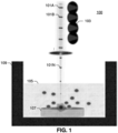
- FIG. 1 is an exemplary schematic of femtosecond laser synthesis system 100.
- the system emits femtosecond laser beam pulses 101A-101N that are directed onto a target 107 submerged in a solvent 105 that is contained within a vessel 109.
- the femtosecond laser beam may be generated using a variety of techniques.
- a Ti:sapphire laser (such as a Coherent Mira 900 laser) is employed for femtosecond laser ablation synthesis, using ⁇ 150 fs pulse width at 800 nm, and operating at a 76 MHz pulse repetition rate.
- FIG. 1 also illustrates the effects 103 of the femtosecond laser beam.
- the target 107 can be chosen from organic or inorganic material.
- the target 107 may also be chosen from a variety of metal, semiconductor, or metal-oxide targets. For example, it can be ZnO, Zn 3 N 2 , GaN, C, Si, CuO, Mn 2 O 3 , and MoS 2 .
- a nanoparticle is a nanoscale particle of semiconducting material that can be embedded in cells or organisms for various experimental purposes, such as labeling proteins, emitting light, etc.
- the solvent 105 that the target 107 is submerged within can been chosen based on the characteristics of the target material 107 (for instance, water may not be an ideal solvent for materials that oxidize easily).
- a vessel 109 such as a glass vessel, may be used to contain the target 107 and the solvent 105.
- TEM images are illustrated of exemplary nanoparticles synthesized by femtosecond laser ablation in accordance with embodiments of the present invention.
- FIG. 2 is a transmission electron microscopy image of manganese oxide (Mn 2 O 3 ) nanoparticles.
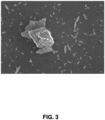
- FIG. 3 is a scanning electron microscope (SEM) image of the MoS 2 nanoparticles.
- sizes of the nanoparticles may fall within the broad range of 2 to 300 nm, and the size of nanoparticle generated using this method is a function of the power of the laser interacting with the target. Accordingly, the laser power can be tuned to produce nanoparticles matching desired sizes. And in this regard, the size of a nanoparticle determines at least some of its physical properties, so the ability to tune the power of the laser provides a significant tool for the generation of nanoparticles having desirable properties.
- the nanoparticles synthesized in accordance with the present invention are crystalline (i.e., no polycrystalline or amorphous phases are observed), indicating that these nanoparticles can be effective active materials for optoelectronic devices.
- the phase of the synthesized materials is determined by X-ray photoelectron spectroscopy (XPS).
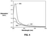
- FIGS. 4 and 5 diagrams are provided that illustrate various characteristics of nanoparticles, including the absorption properties of the nanoparticles, synthesized in accordance with some example embodiments of the present invention.
- FIG. 4 displays the absorption spectra of Mn 2 O 3 nanoparticles synthesized at three different laser powers, resulting in different quantum with different sizes.
- curve 301 illustrates the synthesis of Mn 2 O 3 at 1.85 w
- curve 303 illustrates the synthesis of Mn 2 O 3 at 1.65 w
- curve 305 illustrates the synthesis of Mn 2 O 3 at 1.18 w.
- the absorption rate of Mn 2 O 3 synthesized at 1.85 w peaked between 200 nm and 250 nm wavelengths, having an absorption rate higher than Mn 2 O 3 synthesized at 1.65 w or 1.18 w.
- Fig. 5 displays a Tauc plot of Mn 2 O 3 nanoparticles synthesized at three different laser powers, which illustrates the differences of optical bandgaps as part of optical properties of nanoparticles.
- the bandgap of the nanoparticles can be estimated from Tauc plot.
- curve 302 illustrates the synthesis of Mn 2 O 3 at 1.85 w
- curve 304 illustrates the synthesis of Mn 2 O 3 at 1.65 w
- curve 306 illustrates the synthesis of Mn 2 O 3 at 1.18 w.
- Mn 2 O 3 synthesized at 1.85 w has an energy gap of 4.93 eV
- Mn 2 O 3 synthesized at 1.65 w has an energy gap of 5.16 eV.
- Mn 2 O 3 synthesized at 1.18 w has an energy gap of 5.18 eV.
- Optical characterizations of targets must been carried out to identify the optical properties of the materials shown in FIGS. 4 and 5 .
- different laser parameters power and wavelength in particular
- some example embodiments contemplated herein extend the concept of nanoparticle generation using femtosecond laser ablation synthesis in solvent to a commercial-scale system utilizing multiple synthesis chambers.
- a system utilizing a scaled up scheme for mass production of nanomaterials by femtosecond laser ablation synthesis is followed by a deposition process to apply the generated nanomaterials on the fabricated devices, (as will be described in greater detail herein).
- the system in FIG. 6 includes a femtosecond laser beam generator 402 capable of generating a femtosecond laser beam 404.
- the femtosecond laser beam generator 402 may be a Ti:sapphire laser device able to generate a laser with a pulse duration of 150 femtoseconds, a pulse width of 800 nanometers, and a pulse repetition rate of 76 MHz.
- the power of the femtosecond laser beam 404 is monitored by the power meter 408, and may be adjusted if it is not consistent. As discussed above, the power of the laser beam may change the dimensions and properties of the nanoparticle created by ablation of the semiconductor targets. Therefore, monitoring the power of femtosecond laser beam using power meter 408 enables the system to ensure generation of nanoparticles having consistent optical properties.
- the femtosecond laser beam may further be split by the beam splitters 406A-406N split to ablate multiple targets simultaneously.
- the splitting of the femtosecond laser beam may require adjustment of the total optical power of laser, as the power of each derivative laser beam will be a fraction of the power of the original femtosecond laser beam.
- the femtosecond laser beam 404 may have a total optical power based on a collectively required power for the plurality of semiconductor targets to be ablated, and the beam splitters split the femtosecond laser beam 404 into a plurality of derivative femtosecond laser beams, each having an individual optical power comprising a fraction of the total optical power.
- Each of the beam splitters has a corresponding splitting ratio determining the fraction of the laser directed to a corresponding target, and this splitting ratio may be adjusted in some embodiments based on the individually required power for the corresponding target.
- the targets are preferably submerged in solvent to ensure that generated nanoparticles are captured for later use.
- the targets may be any of ZnO, Zn 3 N 2 , GaN, C, Si, CuO, Mn 2 O 3 , and MoS 2 , although one having ordinary skill in the art will appreciate that other materials may be utilized by the system based on the manufacturing considerations and optical properties relevant to a given industrial application.
- the solvent may be provided through a solvent supply valve 410, and distributed to each synthesis chamber by a corresponding solvent release valve 412A-412C.
- the height of the solvent is critical for ensuring that the target is fully submerged and that nanoparticles created by the ablation process are captured by the solvent.
- the height can be monitored by a sensor 414 that can be attached to the solvent release valves 412A-412C in the solvent supply line for each chamber.
- the level of the solvent can be further monitored by sensors, such as sensor 414, and the height of the solvent can be further adjusted based on the sensed level of the solvent.
- the nanoparticle solution is drained from the synthesis chambers through collection end valves 416A-416C, allowing the solution to be collected in collection chamber 418.
- One or more additional post-collection chambers such as evaporation chamber 420, spraying chamber 422, and coating chamber 424, may be used to further process the nanoparticle solution and utilize the generated nanoparticles.
- the nanoparticle solution can be directed for deposition, or it can be evaporated in the evaporation chamber 420 for a predetermined period of time to generate a nanoparticle powder.
- Further processing is conducted to fabricate optoelectronic devices using nanoparticles. Such processing may be conducted in the spraying chamber 422, which spray-coats the nanoparticles onto a substrate, or in the coating chamber 424, which dip-coats and/or spin-coats the nanoparticles onto substrates.
- Such processes are described below for exemplary purposes, although it will be understood that a wide range of uses of the generated nanoparticles are contemplated herein.
- Systems structured in accordance with embodiments of the present invention provides many advantages.
- the system is readily reproducible, and the consistency of the nanoparticles generated using embodiments of this femtosecond laser ablation synthesis is very high.
- the target material can be used for many synthesis cycles. Therefore, once the power level is optimized, it is possible to repeatedly perform the synthesis process. Moreover, this process does not involve any expensive equipment other than the femtosecond laser itself, along with any proprietary tools for nanoparticle deposition, so example embodiments contemplated can utilize an auto-controlled design.
- optoelectronic devices are fabricated based on Mn 2 O 3 , ZnO, MnS 2 and/or GaN nanoparticles to provide deep ultraviolet and ultraviolet photodetectors, as well as ultraviolet and white light emitting devices.
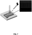
- FIGS. 7 and 8 show examples of fabricated electrodes that could be used to make such devices.
- the process for fabricating electrodes uses the following steps:
- FIG. 7 shows a schematic of the device showing the interdigitated electrode with drop-casted and dried or spray coated nanoparticles.
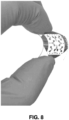
- FIG. 8 shows the design of a fabricated electrode.
- DUV photodetector and sensor technologies operating in the UV-C spectral region ( ⁇ 280 nm) have drawn considerable attention of researchers and practitioners due to their potential applications in diverse fields, such as high-temperature flame detection, missile launch detection, environmental monitoring, binary switching in imaging techniques, remote control, chemical analysis, ozone layer monitoring, secure space-to-space communications, and biological threat detection because of their ability to detect biotoxins.
- a key parameter of a photodetector device is its response time, which determines its capability to detect rapidly varying optical signals. Long carrier lifetime decreases the photodetector response time. A slow time response of a photodetector is attributed to high density of trapped electronic states, which is normally induced by defects. This slow response hinders the practical application of the devices. Therefore, it is very important to maintain the high responsivity and the fast response of photodetector devices.
- Zinc oxide (ZnO) remains a promising material in the development of optoelectronic devices, including DUV photodetectors, due to its wide bandgap (3.3 eV) and high exciton binding energy (60 meV).
- ZnO materials possess high chemical and thermal stability and are naturally abundant and nontoxic.
- ZnO QDs are particularly interesting, owing to their tunable bandgap in the DUV regime. It is well known that the inherent junction barrier between ZnO QDs is highly sensitive to the concentration of photo-generated carriers. Thus, dot-dot junctions in a ZnO QD network should significantly improve conductance under DUV illumination.
- DUV photodetectors based on ZnO QDs have not been implemented in existing methods.
- solution-processed QDs are used as an active layer in fabricating a novel state-of-the-art fixable DUV photodetector by a cost-effective, facile, and simple technique.
- High responsivity, fast response and stable switching performance of DUV photodetectors can be achieved.
- the performance of the device remains extremely stable over several months under ambient conditions without any degradation that is due to water and oxygen molecule species.
- both rigid and flexible substrates are utilized for device fabrication.
- PET polyethylene terephthalate
- a unique synthesis method of ZnO QDs is used by FLAL, which can be applicable to other materials and can be scaled up for higher throughput material synthesis.
- a spraying method as an inexpensive fabrication technique, allows the process to be cost-effective.
- C-doped ZnO QDs are formed from zinc nitride targets.
- DFT density functional theory
- FLAL synthesis under atmospheric conditions may be used.
- FLAL is a simple, fast, versatile and inexpensive method for producing high-quality solution-processed QDs, including C-doped ZnO QDs.
- no post-synthesis (heating, cleaning, etc .) chemical processing is required.
- FLAL synthesis is also faster than a sol-gel method, and a FLAL technique can produce well-crystallized pure nanoparticles (NP) without generating any byproducts.
- a zinc nitride (Zn 3 N 2 ) (such as that provided by AJA International Inc.) target is used as a source material for Zn.
- the Zn 3 N 2 target is the best source material to produce high-quality C-doped ZnO nanoparticles because it requires far less laser power for FLAL synthesis than a pure ZnO target.
- the difference in the ablation laser power threshold for the targets may be attributed to the bond strength between Zn and N or O.
- a titanium-sapphire (coherent-Mira 900) laser with optimum operating conditions of 150 fs pulse width and 76 MHz pulse repetition rate at 800 nm wavelength may be used for FLAL synthesis.
- Laser ablation by using ultra-short femtosecond (fs) pulses provides distinct advantages over continuous wave (CW) or nanosecond (ns) lasers.
- the pulse duration is shorter than the time scale of electron coupling (in the ps range). Any secondary (post-ablation) effects on the QDs can thus be avoided.
- the ultrafast pulses of fs lasers do not affect the material absorption properties and do not interact with ejected species and expanding plasma plumes.
- the incident ultrafast pulses should mostly interact with the target surface, resulting in highly efficient material ablation. Further, thermal damage due to ablation is low relative to CW or ns laser ablation. Therefore, this method may be classified a melt-free ablation process, if carried out close to ablation threshold. Furthermore, FLAL is non-selective to the source material, which enables this process to synthesize many other materials and can be scaled up for higher throughput device fabrication.
- interdigitated electrodes may be prepared using photolithography on silicon oxide substrate (SiO 2 ) followed by e-beam evaporation (for example, Oxford Instrument. U.K.) of titanium.
- SiO 2 silicon oxide substrate
- e-beam evaporation for example, Oxford Instrument. U.K.
- FIGS. 26 and 31 were prepared in this way.
- shadow-mask technique using the e-beam evaporation may be implemented.
- the device illustrated in FIG. 32 (using flexible PET substrate) is prepared this way.
- the Ti electrode thickness remained at 100 nm, and the distance between the electrodes was 20 ⁇ m.
- the device illustrated in FIG. 26 is prepared by drop casting 10 ml of colloidal QD solution over time, with the substrate temperature kept constant at 100 °C.
- the device illustrated in FIG. 31 is prepared by spray coating 10 ml of colloidal QD solution on a heated (100 °C) substrate
- the (flexible) device illustrated in FIG. 32 is prepared by spray coating 10 ml of colloidal QD solution on an interdigitated titanium (Titanium) electrode (ITD) deposited on polyethylene terephthalate (PET) substrate.
- ITD interdigitated titanium
- PET polyethylene terephthalate
- the PET substrate was kept on a hotplate at 50 °C.
- the solution was sprayed on the PET substrate for a precise amount of time for 5min using a small volume, such as 2 ml, each time.
- the calculations were performed at the gamma point, and a plane-wave cutoff energy of 500 eV was used to describe the basis set.
- the cluster was optimized within a force tolerance of 0.01 eV/ ⁇ to minimize the Hellmann-Feynman forces on each atom.
- a HeAg pulsed (Laser 2000 UK Ltd.) laser with a 224.3 nm wavelength was used for illumination.
- the laser repetition rate remained at 1 Hz throughout the experiments.
- a probe station was attached to a Keithley 2400 SourceMeter (for example, Tektronix, China).
- the laser pulse width remained below 200 ⁇ s.
- FIGS. 9-13 illustrate results obtained via a Titan 60-300 microscope (obtained from FEI Co) equipped with Cs probe corrector and imaging filter Quantum 966, operated at 200kV in STEM mode.
- FIG. 9 is a TEM image of ZnO QDs.
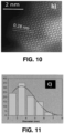
- FIG. 10 is a TEM image of ZnO QDs exhibiting typical fringes of crystalline structures.
- FIG. 11 illustrates an average particle diameter (3.4 ⁇ 1.7 nm) as measured in several low-resolution images.
- EELS compositional maps of QDs of O, Zn, and C are illustrated in FIG. 12.
- FIG. 13 illustrates EDX measurements of the ZnO QDs confirming the presence of C, Zn and O.
- HR-TEM transmission electron microscopy
- EELS electron energy-loss spectroscopy
- the TEM image in FIG. 9 shows the crystallinity (wurtzite structure) of QDs that were drop-casted and dried on copper (Cu) TEM grids.
- the d-spacing of ⁇ 0.28 nm corresponds to the (100) plane, as shown in FIG. 10 .
- the size distribution shown in FIG. 11 indicates an average particle diameter of 3.4 ⁇ 1.7 nm.
- FIG. 12 shows the EELS maps of QD elemental compositions, indicating that the ZnO QDs are composed of Zn and O, with heavy presence of C dopants.
- the heavy C doping is confirmed by energy-dispersive x-ray (EDX) spectroscopy, as shown in FIG. 13 .
- C atoms can occupy both Zn-vacancy (V Zn ) and O-vacancy (Vo) sites and C dopants were found to prefer substitutional Vo sites in ZnO structures.
- the substitutional defects depend on the synthesis process.
- the characteristics outlined above may be generated from a system in which the primary material for ablation is a zinc nitride target and the ablation is carried out in an ethanol solution.
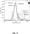
- FIGS. 14 and 15 illustrate Core-level XPS spectra: FIG. 14 illustrates high-resolution XPS C 1s spectrum, and FIG. 15 illustrates O 1s spectrum of the C-doped ZnO QD samples.
- FIG. 14 shows the C 1s core-level spectrum, indicating a broad asymmetric peak.
- the peak is fitted by a Gaussian function, which is de-convoluted into four peaks.
- the asymmetric behavior of the peak implies presence of more than one chemical state of C.
- the lower binding energy peaks at 284.73 eV and 283.41 eV are attributed to pure graphitic C contamination and Zn-C-VO bonding, respectively. It further suggests the presence of C atoms in carbide form, indicating that C dopants occupy the substitutional anion sites and facilitate formation of Zn-C bonds in the C-doped ZnO QDs.
- the deconvolution of the O 1s peak in FIG. 15 reveals binding energies at 529.89 eV and 531.07 eV, which respectively correspond to the Zn-O bond and surface adsorption of - OH functional group. This result is confirmed by Fourier transform infrared spectroscopy (FTIR) measurements, as shown in FIG. 16 .
- FTIR Fourier transform infrared spectroscopy
- FTIR analysis was carried out on as-prepared samples and the findings were compared to those pertaining to an aged sample, as shown in FIG. 16 .
- FTIR spectra indicate that surface termination likely exists in the sample.
- FTIR spectra were obtained by employing attenuated total reflectance mode (ATR) in the 500-4000 cm -1 wavelength range. The emergence of a broad band peak at 3200-3500 cm -1 is observed, which is attributed to the presence of the hydroxyl on the material surface. Specifically, H-OH stretching contributes to the peak at 3435 cm -1 , while those noted at 3446 cm -1 and 3500 cm -1 correspond to the O-H stretching mode.
- ATR attenuated total reflectance mode
- This broad peak is enhanced in the spectrum pertaining to the aged sample, which was synthesized in ethanol, due to which -OH terminations gradually emerge at the particle surface over time.
- the symmetric and asymmetric C-H stretching nodes of -CH 2 group shown in FIG. 16 overlap with the broad signal pertaining to O-H group.
- the peaks located between 2800 cm -1 and 3000 cm -1 correspond to C-H stretching vibration of the alkane group.
- Asymmetrical stretching of Zn carboxylate is also observed at ⁇ 1630 cm -1 .
- the peaks located around 1454 cm -1 and 1384 cm -1 correspond to stretching and wagging of CH 2 . This result confirms the contribution of carbon-related components and hydroxyl group on the surface of QDs.
- FTIR spectrum suggests that QD surface-termination is of the -R type, which prevents further oxidation of the core level of the QDs.
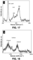
- FIGS. 17 and 18 depict the Raman spectra of C-doped ZnO quantum dots (QDs), where FIG. 17 illustrates Raman spectra originating from ZnO QDs, and FIG. 18 illustrates spectra showing presence of G and D band of carbon. All Raman measurements were performed using WiTec Raman system, equipped with 532 nm laser source, 100 ⁇ objective, and 600 lines/mm grating. ZnO QDs were drop-casted and dried on calcium fluoride (CaF 2 ) substrate.
- QDs C-doped ZnO quantum dots
- the Raman spectra show a clear contribution of ZnO QDs, C-H vibration, and C-cluster.
- the sharp peak at around 317 cm -1 is related to the Ca-F vibration of the substrate over which the ZnO QDs sample was drop-casted.
- the peak at 438 cm -1 is attributed to the ZnO wurtzite structure, specifically to the E 2 (high) vibration mode of ZnO, as shown in FIG. 17 .
- the second peak observed at 566 cm -1 is attributed to the E 1 (LO) ZnO nanostructure mode.
- the peak corresponding to pure ZnO is attributed to the intrinsic defect states.
- the peak located in the lowering wavenumber is probably attributed to the Zn-C bonds.
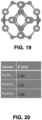
- FIG. 19 illustrates the optimized Zn12O12 cluster.
- the grey and red spheres indicate Zn and O atoms, respectively.
- FIG. 20 illustrates the formation energy of defects (Ef) in Zn12O12 cluster.
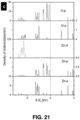
- FIG. 21 illustrates the density of states (DOS) of a Zn12O12 (corresponding to pure ZnO QDs), and
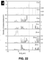
- FIG. 22 illustrates Zn12O10C1 (corresponding to C-doped ZnO QDs with the presence of VO defects) clusters.
- FIG. 19 shows a "magic" ZnO cluster (Zn12O12) with a hexagonal structure corresponding to the structure of ZnO QDs.
- Zn12O12 an O vacancy
- CO carbon substituted to the O site
- VO+CO a carbon substituted to the O site
- Ef E D ⁇ E R ⁇ ni ⁇ i
- first term (E(D)) represents the total energy of the cluster containing defects
- second term (E(R)) denotes the total energy of the reference cluster without defects
- ni and ⁇ i are respectively the number and chemical potential of the defects that are added (-ni) or removed (+ni) from the cluster.
- the chemical potential was estimated as the energy per atom of the element in the most stable structure in this case, bulk Zn or molecular C and O.
- the density of states (DOS) of the Zn12O12 (pristine ZnO) and Zn12O10C1 (ZnO doped with the C-VO complex) clusters was calculated for a qualitative comparison with the experimental results.
- the DOS of the Zn12O12 cluster shows that the p states of Zn and O are prominent and are located near the Fermi level (EF), while the Zn d state occurs deep inside the valence band as shown in FIG. 21 .
- C doping in the ZnO structure reduces the chance of recombination, subsequently enhancing photocurrent generation. Consequently, carbon-doped nanostructures have been used in photocatalysis. Therefore, the expectation here is that C doping in ZnO QDs would indirectly influence photodetector device performance.
- FIGS. 23 and 24 absorption spectroscopy measurements were performed to investigate the change in the bandgap due to the change in the surface states (surface passivation over time).
- FIG. 23 illustrates the absorption spectra of QDs in ethanol over days of aging
- FIG. 24 illustrates tauc plot of the direct band gap of as-prepared QDs and after 6 days aging in ethanol.
- the inset in FIG. 24 shows the shoulder peak appears after ageing.
- FIG. 23 shows the absorption spectra of the colloidal QDs over several days of ageing in ethanol.
- the spectrum of as-prepared sample does not show a pronounced absorption edge at bulk ZnO band gap at 3.64 eV.
- the measured band gap energy is observed at 4.9 eV as shown in FIG. 24 .
- a shoulder peak at 3.64 eV related to ZnO bulk appears as shown clearly in the Tauc plot in FIG. 24 . This shoulder peak is attributed to the surface oxidation of the QDs.
- the core of the as-prepared QDs has O deficiency, because the QDs are prepared from a zinc nitride target.
- the as-prepared sample exhibits higher absorption in the visible region compared to the aged samples, which have lower absorbance in the visible region.
- the higher-energy absorption edge in the visible region of the as-prepared samples is attributed to the C doping; however, the oxidation process leads to passivation, which reduces the absorption and results in a blueshift in the absorption edge of the aged samples over the investigated period.
- the passivation process on the surface of the QDs completely stabilized after six days, and no significant changes in the optical properties were observed for many months after that. The absorption results indicate superior stability and surface passivation of the QDs in colloidal form.
- the average particle size is 4.6 nm, which is close to the average size determined by TEM.
- the direct bandgap of the ZnO bulk at pH 7.5 is 3.63 eV (Ebulk).
- the above equation yielded an average particle size of 4.6 nm, which is close to the average particle size measured from the TEM images.
- FIG. 25 (upper panel) is a schematic illustration of FLAL synthesis with QDs coated on the interdigitated titanium electrode on rigid and flexible substrates.
- the (lower panel) photodetector devices are exposed to a 224.3 nm HeAg pulsed laser.
- the repetition rate of the laser pulse with a pulse width of 200 ⁇ s remains constant at 1 Hz throughout the photodetector measurements.
- FIG. 26 illustrates the transient photo-response of a device prepared by a drop-casting method on a SiO2 substrate at different bias voltages.
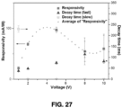
- FIG. 27 illustrates the responsivity (left axis) and the decay time (right axis) of the device as functions of bias voltage.
- FIG. 25 the schematic shows the steps and method of device preparation.
- FIG. 26 presents the transient photoresponse under pulsed DUV illumination at different bias voltages.
- colloidal nanoparticles in ethanol are coated on the electrode (e.g., an interdigitated titanium (Ti) electrode (ITD)) to produce photodetector devices.
- the electrode e.g., an interdigitated titanium (Ti) electrode (ITD)
- ITD interdigitated titanium
- such devices may be fabricated on rigid substrates (SiO2 wafers), and in other embodiments, such devices may be frabricated on flexible substrates (PET).
- the transient photoresponse of example photodetector devices (prepared by a drop-casting method on a SiO2 substrate) was measured under pulsed DUV illumination at different bias voltages.
- the laser excitation of the photodetector at 5.5 eV (224.3 nm) was well above that of the nanoparticle bandgap of 4.9 eV.
- the device Under pulsed laser illumination, at bias voltages of 1 V, 2 V and 5 V, the device exhibited a stable response over time, as illustrated in FIGS. 26 and 27 .
- the response time was examined. To calculate the response time, the curves shown in FIG. 26 needed to be fit. All the curves were fitted by an exponential function.
- the decay time at 1 V bias voltage exhibits double exponential response, as it has a fast (37.58 ms) and a slow (230 ms) component.
- the decay time follows a single exponential form.
- the decay and rise time in milliseconds indicates that devices created using example embodiments contemplated herein can work as an ultrafast photodetector. Accordingly, the cost effective devices generated based on the solution process contemplated herein provides both high performance and enables fabrication in flexible substrates and with high responsivity.
- the responsivity of examples generated in accordance with example embodiments described herein is 100 times lower than that of a historically generated deep ultraviolet photodetector.
- FIG. 28 shows photo-response under pulsed DUV illumination at different bias voltages under illumination of 224 nm (5.5 eV) pulsed laser with energy, which is well above the 4.9 eV bandgap of the QDs.
- Photodetector responses obtained under different bias voltages revealed that, at lower bias, the response is much more stable, as shown in FIG. 27 .
- Under pulsed laser illumination, at 1 V, 2 V and 5 V bias a very stable response over time is obtained. This stability does not persist at higher bias voltages (> 5 V), as the transient photocurrent changes at different times, as shown in FIG. 28 .
- fast response in ms
- responsivity up to ⁇ 100 mA/W
- FIGS. 29 and 30 show the fitting of the decay time at different bias voltages for the device shown in FIGS. 26 and 27 .
- the fitting procedure adopted to measure the decay time is in line with that used by others.
- Iph is the photo current
- A1 and A2 are coefficients
- t denotes the time
- ⁇ slow and ⁇ fast are the slow and fast respective time constants
- Ioffset is the current offset level.
- A2 ⁇ A1 indicates that the ⁇ fast component dominates, due to which the decay time declines rapidly.
- the rise time corresponds to the change in current from 0 to
- FIG. 27 presents a comparison of the decay time and the responsivity of device shown in FIG. 26 at different voltages.
- the decay time at 1 V bias voltage has a double exponential response with fast (37.58 ms) and slow (230 ms) components.
- the decay time for the bias voltages above 1V has a single exponential response.
- FIGS. 29 and 30 Fitting of the rise time and the decay time is illustrated in FIGS. 29 and 30 .
- the device shows ultrafast response (the slow component disappeared) compared with the DUV devices based on films, as well as nanoparticles.
- the device shown in FIGS. 26 and 27 works optimally in the 2-5 V range due to its very high responsivity, its fast response time and its significant stability in this voltage regime.
- FIG. 31 illustrates transient photocurrent generation under DUV illumination for a device prepared on a rigid substrate with the airbrush spray-coating technique.
- the average responsivity is 295 ⁇ 4 mA/W at 5 V bias voltage.
- FIG. 32 illustrates transient photocurrent generation under DUV illumination for the device shown in FIG. 32 (the flexible PET substrate with the airbrush spray-coating technique).
- the average responsivity is 88.4 ⁇ 0.7 at 5 V bias.
- FIG. 33 illustrates responsivity measurement of this device as a function of the number of bending. The inset photos show this device bending.
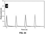
- FIG. 34 illustrates photocurrent generation after various numbers of bending at certain degree angle.
- FIGS. 31 shows that the photocurrent generation of its device, with an average responsivity of 295 ⁇ 4 mA/W, which is higher than that of the device shown in FIGS. 26 and 27 .
- the transient photoresponse of the device shown in FIG. 32 indicates a responsivity of 88.4 ⁇ 0.7 at 5 V bias.
- the responsivity values of the three devices are the highest achieved to date in solution-processed QD-based DUV photodetectors. Moreover, they are superior to those of state-of-the-art UV photodetectors, including the commercial products, as described in detail hereinafter.
- FIG. 33 shows the responsivity of the flexible device from FIG. 32 after 150 cycles of bending at a certain degree angle (up to 30°) (the photographs in FIG. 33 show the bending setup used for this measurement), indicating that the device is immune to stress and its performance is not affected by bending process.
- FIG. 34 shows the transient photoresponse as a function of the number of bending cycles, which further confirms that photocurrent generation remains unchanged after even 150 cycles of bending.
- the response time (rise time and decay time) remains below than 85 ms in the 2-5 V range, which is as fast as previously reported results of solution-processed NANOPARTICLE-based DUV devices and also faster than thin film DUV photodetectors. Visible blindness characteristics are crucial in DUV photodetectors.
- Table 1 below lists some results reported in pertinent studies and the responsivity of the different devices described therein, in comparison with the responsivity of an embodiment of the present invention.
- the bottom row of Table 1 illustrates an example embodiments described herein (a Schottky junction photodetector fabricated using the spray coating technique) that exhibited a response parameter of 295 mA/W @ 224 nm.
- Table 1 also shows a comparison of UV/DUV photodetectors fabricated by different methods, along with their responsivity at a specific wavelength. Table 1.
- Table 2 below shows the results of systems structured in accordance with embodiments of the present invention: Table 2. Characteristics of Deep Ultraviolet Photodetector fabricated using systems structured in accordance with embodiments of the present invention No. Material Responsivity Time Wavelength Process Involved a ZnO QDs by FLA synthesis 295 mA/W less than 80ms 224 nm laser Solution processed
- LEDs Ultraviolet and White Light-emitting diodes
- the optoelectronic devices fabricated in accordance with claimed invention can be cost-effective bright white light LEDs based on nanoparticles such as quantum dots.
- white LEDs are fabricated using very expensive GaN materials that require costly fabrication methods, such as metal-organic chemical vapor deposition (MOCVD) and molecular beam epitaxy (MBE).
- MOCVD metal-organic chemical vapor deposition
- MBE molecular beam epitaxy
- the final product is very expensive and is affected by threading dislocation defects arising from lattice mismatch substrate.
- the techniques described above for generation of nanoparticles and fabrication of an electrode using the nanoparticles are employed to produce white light emission more efficiently at a lower cost than historical methods.
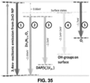
- FIG. 35 illustrates the emission of an example white emitting LED generated in this manner.
- FIG. 36 illustrates photoluminescence information regarding the example white light LED.
- FIG. 37 illustrates the I-V curve of the example white light LED.
- FIG. 38 shows the structure of the example white LED.
Landscapes
- Chemical & Material Sciences (AREA)
- Organic Chemistry (AREA)
- Chemical Kinetics & Catalysis (AREA)
- Physics & Mathematics (AREA)
- Engineering & Computer Science (AREA)
- Nanotechnology (AREA)
- Electromagnetism (AREA)
- Inorganic Chemistry (AREA)
- Optics & Photonics (AREA)
- Health & Medical Sciences (AREA)
- General Health & Medical Sciences (AREA)
- Toxicology (AREA)
- Crystallography & Structural Chemistry (AREA)
- Manufacturing & Machinery (AREA)
- General Physics & Mathematics (AREA)
- Condensed Matter Physics & Semiconductors (AREA)
- Physical Or Chemical Processes And Apparatus (AREA)
- Luminescent Compositions (AREA)
Claims (13)
- Verfahren zum Herstellen einer optoelektronischen Vorrichtung, das Verfahren umfassend:Erzeugen, durch einen Laserstrahlgenerator, eines Laserstrahls;Teilen, durch einen Satz von Strahlteilern, des Laserstrahls in Teile des Laserstrahls; undAusrichten der Teile des Laserstrahls auf die Vielzahl von Zielen, wobei jedes der Vielzahl von Zielen in ein entsprechendes Syntheselösungsmittel getaucht ist und jeder der Teile des Laserstrahls durch einen oder mehrere der Strahlteiler auf sein entsprechendes Ziel gerichtet wird,wobei eine Wechselwirkung von jedem Teil des Laserstrahls mit einem entsprechenden Ziel der Vielzahl von Zielen Nanopartikel in das entsprechende Syntheselösungsmittel freisetzt, um eine Nanopartikellösung zu schaffen, die sowohl Syntheselösungsmittel als auch freigesetzte Nanopartikel beinhaltet,dadurch gekennzeichnet, dassjedes der Vielzahl von Zielen in einer entsprechenden Synthesekammer ist, das Verfahren ferner umfassendSammeln, in einer Sammelkammer, der Nanopartikellösung aus mindestens einer der mehreren Synthesekammern; undAufbringen der gesammelten Nanopartikellösung auf ein Substrat mit ineinandergreifenden Elektroden, um eine optoelektronische Vorrichtung zu bilden, wobei ein Aufbringen der gesammelten Nanopartikellösung auf ein Substrat ein Sprühbeschichten, Tauchbeschichten oder Schleuderbeschichten des Substrats mit der Nanopartikellösung umfasst.
- Verfahren nach Anspruch 1, wobei der Laserstrahl eine Wellenlänge in einem Bereich von ultravioletter bis infraroter Strahlung und eine Pulswiederholungsrate in einem Bereich von KHz bis MHz aufweist.
- Verfahren nach einem der Ansprüche 1 bis 2, wobei die Vielzahl von Zielen ausgewählt ist aus der Gruppe, bestehend aus organischem Material und anorganischem Material.
- Verfahren nach Anspruch 1, ferner umfassend:Übertragen mindestens eines Teils der Flüssigkeit aus der Sammelkammer zu einer Verdampfungskammer; undVerdampfen des Lösungsmittels aus der Nanopartikellösung in der Verdampfungskammer, um einen Nanopartikelpulverrest zurückzulassen.
- Verfahren nach einem der Ansprüche 1 bis 4, ferner umfassend für jede Synthesekammer:Empfangen einer Angabe über einen gewünschten Flüssigkeitsstand in der Synthesekammer;Erfassen, über einen Füllstandsensor, eines tatsächlichen Flüssigkeitsstands in der Synthesekammer; undin einem Fall, in dem der tatsächliche Flüssigkeitsstand der Synthesekammer unter dem gewünschten Flüssigkeitsstand ist, Einstellen eines Ablassventils, das mit der Synthesekammer assoziiert ist, um zu bewirken, dass Syntheselösungsmittel in die Synthesekammer fließt, bis der tatsächliche Flüssigkeitsstand der Synthesekammer den gewünschten Flüssigkeitsstand erreicht.
- Verfahren nach einem der Ansprüche 1 bis 5, ferner umfassend:Überwachen, unter Verwendung eines Leistungsmessgeräts, der Leistung des Laserstrahls; undin einem Fall, in dem die Leistung des Laserstrahls um einen vorbestimmten Schwellenwert von einem Soll-Leistungspegel abweicht, Anpassen der Leistung des Laserstrahls durch den Laserstrahlgenerator, bis die Leistung des Laserstrahls dem Soll-Leistungspegel entspricht.
- Verfahren nach Anspruch 1, wobei die Vielzahl von Zielen Zinknitrid-Ziele und die Nanopartikel C-dotierte Zinkoxid-Nanopartikel sind.
- Verfahren nach Anspruch 1, wobei die Vielzahl von Targets eines von ZnO-, Zn3N2-, GaN-, C-, Si-, CuO-, Mn2O3- und MoS2-Zielen ist.
- System zum Herstellen einer optoelektronischen Vorrichtung, das System umfassend:einen Laserstrahlgenerator, der konfiguriert ist, um einen Laserstrahl zu erzeugen;eine Vielzahl von Synthesekammern, die jeweils ein Ziel unterbringen, das in ein Syntheselösungsmittel getaucht ist; undeinen Satz von Strahlteilern, die angeordnet sind, um einen Laserstrahl, der von dem Laserstrahlgenerator erzeugt wird, in eine Vielzahl von abgeleiteten Laserstrahlteilen zu teilen, die auf entsprechende Ziele gerichtet sind,wobei eine Wechselwirkung von jedem Teil der abgeleiteten Laserstrahlteile mit seinem entsprechenden Ziel Nanopartikel in das entsprechende Syntheselösungsmittel freisetzt, um eine Nanopartikellösung zu schaffen, die sowohl das entsprechende Syntheselösungsmittel als auch die freigesetzten Nanopartikel beinhaltet,gekennzeichnet durcheine Sammelkammer, die mit einer oder mehreren der Synthesekammern verbunden ist, um Nanopartikellösung aus mindestens einer der mehreren Synthesekammern zu erhalten; undKomponenten, die konstruiert sind, um die gesammelte Nanopartikellösung auf ein Substrat mit ineinandergreifenden Elektroden aufzubringen, um eine optoelektronische Vorrichtung zu bilden, wobei die Komponenten, die konstruiert sind, um die gesammelte Nanopartikellösung auf das Substrat aufzubringen, eine Sprühkammer sind, die konstruiert ist, um Nanopartikel der Nanopartikellösung auf das Substrat zu sprühen, oder eine Beschichtungskammer sind, die konstruiert ist, um die Nanopartikel der Nanopartikellösung durch Sprühbeschichten oder Schleuderbeschichten auf das Substrat aufzubringen.
- System nach Anspruch 9, wobei der Laserstrahl eine Wellenlänge in einem Bereich von ultravioletter bis infraroter Strahlung und eine Pulswiederholungsrate in einem Bereich von kHz bis MHz aufweist.
- System nach einem der Ansprüche 9 oder 10, wobei die Vielzahl der Ziele ausgewählt ist aus der Gruppe, bestehend aus organischem Material und anorganischem Material.
- System nach Anspruch 11, wobei die Vielzahl von Zielen Zinknitrid-Ziele und die Nanopartikel C-dotierte Zinkoxid-Nanopartikel sind.
- System nach Anspruch 11, wobei die Vielzahl von Targets eines von ZnO-, Zn3N2-, GaN-, C-, Si-, CuO-, Mn2O3- und MoS2-Zielen ist.
Applications Claiming Priority (3)
| Application Number | Priority Date | Filing Date | Title |
|---|---|---|---|
| US201762511831P | 2017-05-26 | 2017-05-26 | |
| US201862632296P | 2018-02-19 | 2018-02-19 | |
| PCT/IB2018/053484 WO2018215893A1 (en) | 2017-05-26 | 2018-05-17 | Method and apparatus for fabricating high performance optoelectronic devices |
Publications (2)
| Publication Number | Publication Date |
|---|---|
| EP3630348A1 EP3630348A1 (de) | 2020-04-08 |
| EP3630348B1 true EP3630348B1 (de) | 2024-04-24 |
Family
ID=62749119
Family Applications (1)
| Application Number | Title | Priority Date | Filing Date |
|---|---|---|---|
| EP18734291.0A Active EP3630348B1 (de) | 2017-05-26 | 2018-05-17 | Verfahren und vorrichtung zur herstellung hochleistungsfähiger optoelektronischer vorrichtungen |
Country Status (3)
| Country | Link |
|---|---|
| US (1) | US11571675B2 (de) |
| EP (1) | EP3630348B1 (de) |
| WO (1) | WO2018215893A1 (de) |
Families Citing this family (7)
| Publication number | Priority date | Publication date | Assignee | Title |
|---|---|---|---|---|
| EP3912196A1 (de) * | 2019-01-17 | 2021-11-24 | King Abdullah University of Science and Technology | Tiefe uv-vorrichtungen unter verwendung von ultravioletten nanopartikeln mit p-leitfähigkeit |
| CN112967947B (zh) * | 2020-06-16 | 2023-03-24 | 重庆康佳光电技术研究院有限公司 | 一种去除金属镓的装置及方法 |
| US12183846B2 (en) | 2020-06-16 | 2024-12-31 | Chongqing Konka Photoelectric Technology Research Institute Co., Ltd. | Device and method for removing metal gallium, and laser lift-off system |
| EP4189148A4 (de) * | 2020-07-30 | 2024-09-18 | Krishnan Venkatakrishnan | Ultrakurze lasersynthese von isotopennanopartikeln |
| CN113937181B (zh) * | 2021-09-22 | 2024-04-23 | 香港城市大学成都研究院 | 一种柔性氧化锌纳米颗粒紫外光探测器及其制备方法 |
| CN114678431B (zh) * | 2022-03-21 | 2024-11-26 | 上海集成电路制造创新中心有限公司 | 一种光电探测器的制备方法 |
| CN115283684A (zh) * | 2022-08-05 | 2022-11-04 | 大连理工大学 | 一种使用液相激光烧蚀法连续制备纳米颗粒的装置 |
Family Cites Families (3)
| Publication number | Priority date | Publication date | Assignee | Title |
|---|---|---|---|---|
| WO2010073388A1 (ja) | 2008-12-26 | 2010-07-01 | 株式会社荏原製作所 | 液中レーザーアブレーションシステムおよび固形物微細化方法 |
| US8246714B2 (en) * | 2009-01-30 | 2012-08-21 | Imra America, Inc. | Production of metal and metal-alloy nanoparticles with high repetition rate ultrafast pulsed laser ablation in liquids |
| FR2998485B1 (fr) | 2012-11-26 | 2015-01-02 | Commissariat Energie Atomique | Dispositif pour la synthese de nanoparticules de type cœur-coquille par pyrolyse laser et procede associe. |
-
2018
- 2018-05-17 US US16/613,233 patent/US11571675B2/en active Active
- 2018-05-17 WO PCT/IB2018/053484 patent/WO2018215893A1/en not_active Ceased
- 2018-05-17 EP EP18734291.0A patent/EP3630348B1/de active Active
Also Published As
| Publication number | Publication date |
|---|---|
| WO2018215893A1 (en) | 2018-11-29 |
| US11571675B2 (en) | 2023-02-07 |
| EP3630348A1 (de) | 2020-04-08 |
| US20200197897A1 (en) | 2020-06-25 |
Similar Documents
| Publication | Publication Date | Title |
|---|---|---|
| US11571675B2 (en) | Method and apparatus for fabricating high performance optoelectronic devices | |
| Goswami et al. | GaN nanotowers grown on Si (111) and functionalized with Au nanoparticles and ZnO nanorods for highly responsive UV photodetectors | |
| Ismail et al. | Preparation and characterization of carbon nanotubes by pulsed laser ablation in water for optoelectronic application | |
| Lee et al. | High-responsivity deep-ultraviolet-selective photodetectors using ultrathin gallium oxide films | |
| Goswami et al. | Graphene quantum dot-sensitized ZnO-nanorod/GaN-nanotower heterostructure-based high-performance UV photodetectors | |
| Mitra et al. | Solar-blind self-powered photodetector using solution-processed amorphous core–shell gallium oxide nanoparticles | |
| Mitra et al. | High-performance solar-blind flexible deep-UV photodetectors based on quantum dots synthesized by femtosecond-laser ablation | |
| Alsultany et al. | A high-sensitivity, fast-response, rapid-recovery UV photodetector fabricated based on catalyst-free growth of ZnO nanowire networks on glass substrate | |
| Park et al. | Ag2O/β-Ga2O3 heterojunction-based self-powered solar blind photodetector with high responsivity and stability | |
| Su et al. | Wide range bandgap modulation based on ZnO-based alloys and fabrication of solar blind UV detectors with high rejection ratio | |
| Chen et al. | Ta-doped Ga2O3 epitaxial films on porous p-GaN substrates: structure and self-powered solar-blind photodetectors | |
| Kumar et al. | Low bias operated, fast response SnSe thin film Vis-NIR photodetector on glass substrate using one-step thermal evaporation technique | |
| Kang et al. | Ultraviolet-C photodetector fabricated using Si-doped n-AlGaN nanorods grown by MOCVD | |
| Almalawi et al. | Enhanced UV emission of GaN nanowires functionalized by wider band gap solution-processed p-MnO quantum dots | |
| Pant et al. | Highly responsive, self-powered a-GaN based UV-A photodetectors driven by unintentional asymmetrical electrodes | |
| Sun et al. | Electrical and electroluminescence properties of As-doped p-type ZnO nanorod arrays | |
| Wu et al. | Controlling defect formation of nanoscale AlN: toward efficient current conduction of ultrawide‐bandgap semiconductors | |
| JP7551631B2 (ja) | シーディングまたは触媒を使わずにパルスレーザー堆積法によって成長させた無転位半導体ナノ構造 | |
| Abdulrahman | The effect of different substrate-inclined angles on the characteristic properties of ZnO nanorods for UV photodetectors applications | |
| Dai et al. | ZnO homojunction UV photodetector based on solution-grown Sb-doped p-type ZnO nanorods and pure n-type ZnO nanorods | |
| Khan et al. | Ultra-violet photo-response characteristics of p-Si/i-SiO2/n-ZnO heterojunctions based on hydrothermal ZnO nanorods | |
| Bashkany et al. | A self-powered heterojunction photodetector based on a PbS nanostructure grown on porous silicon substrate | |
| US11862742B2 (en) | Deep ultra-violet devices using ultra-violet nanoparticles with p-type conductivity | |
| Mahmood et al. | Growth and conductivity enhancement of N-doped ZnO nanorod arrays | |
| Selman et al. | Effects of variations in precursor concentration on the growth of rutile TiO2 nanorods on Si substrate with fabricated fast-response metal–semiconductor–metal UV detector |
Legal Events
| Date | Code | Title | Description |
|---|---|---|---|
| STAA | Information on the status of an ep patent application or granted ep patent |
Free format text: STATUS: UNKNOWN |
|
| STAA | Information on the status of an ep patent application or granted ep patent |
Free format text: STATUS: THE INTERNATIONAL PUBLICATION HAS BEEN MADE |
|
| PUAI | Public reference made under article 153(3) epc to a published international application that has entered the european phase |
Free format text: ORIGINAL CODE: 0009012 |
|
| STAA | Information on the status of an ep patent application or granted ep patent |
Free format text: STATUS: REQUEST FOR EXAMINATION WAS MADE |
|
| 17P | Request for examination filed |
Effective date: 20191205 |
|
| AK | Designated contracting states |
Kind code of ref document: A1 Designated state(s): AL AT BE BG CH CY CZ DE DK EE ES FI FR GB GR HR HU IE IS IT LI LT LU LV MC MK MT NL NO PL PT RO RS SE SI SK SM TR |
|
| AX | Request for extension of the european patent |
Extension state: BA ME |
|
| DAV | Request for validation of the european patent (deleted) | ||
| DAX | Request for extension of the european patent (deleted) | ||
| STAA | Information on the status of an ep patent application or granted ep patent |
Free format text: STATUS: EXAMINATION IS IN PROGRESS |
|
| 17Q | First examination report despatched |
Effective date: 20230512 |
|
| P01 | Opt-out of the competence of the unified patent court (upc) registered |
Effective date: 20230621 |
|
| GRAP | Despatch of communication of intention to grant a patent |
Free format text: ORIGINAL CODE: EPIDOSNIGR1 |
|
| STAA | Information on the status of an ep patent application or granted ep patent |
Free format text: STATUS: GRANT OF PATENT IS INTENDED |
|
| INTG | Intention to grant announced |
Effective date: 20231115 |
|
| GRAS | Grant fee paid |
Free format text: ORIGINAL CODE: EPIDOSNIGR3 |
|
| GRAA | (expected) grant |
Free format text: ORIGINAL CODE: 0009210 |
|
| STAA | Information on the status of an ep patent application or granted ep patent |
Free format text: STATUS: THE PATENT HAS BEEN GRANTED |
|
| AK | Designated contracting states |
Kind code of ref document: B1 Designated state(s): AL AT BE BG CH CY CZ DE DK EE ES FI FR GB GR HR HU IE IS IT LI LT LU LV MC MK MT NL NO PL PT RO RS SE SI SK SM TR |
|
| REG | Reference to a national code |
Ref country code: GB Ref legal event code: FG4D |
|
| REG | Reference to a national code |
Ref country code: CH Ref legal event code: EP |
|
| REG | Reference to a national code |
Ref country code: DE Ref legal event code: R096 Ref document number: 602018068523 Country of ref document: DE |
|
| REG | Reference to a national code |
Ref country code: IE Ref legal event code: FG4D |
|
| REG | Reference to a national code |
Ref country code: LT Ref legal event code: MG9D |
|
| REG | Reference to a national code |
Ref country code: NL Ref legal event code: MP Effective date: 20240424 |
|
| REG | Reference to a national code |
Ref country code: AT Ref legal event code: MK05 Ref document number: 1679011 Country of ref document: AT Kind code of ref document: T Effective date: 20240424 |
|
| PG25 | Lapsed in a contracting state [announced via postgrant information from national office to epo] |
Ref country code: NL Free format text: LAPSE BECAUSE OF FAILURE TO SUBMIT A TRANSLATION OF THE DESCRIPTION OR TO PAY THE FEE WITHIN THE PRESCRIBED TIME-LIMIT Effective date: 20240424 |
|
| PG25 | Lapsed in a contracting state [announced via postgrant information from national office to epo] |
Ref country code: NL Free format text: LAPSE BECAUSE OF FAILURE TO SUBMIT A TRANSLATION OF THE DESCRIPTION OR TO PAY THE FEE WITHIN THE PRESCRIBED TIME-LIMIT Effective date: 20240424 |
|
| PG25 | Lapsed in a contracting state [announced via postgrant information from national office to epo] |
Ref country code: IS Free format text: LAPSE BECAUSE OF FAILURE TO SUBMIT A TRANSLATION OF THE DESCRIPTION OR TO PAY THE FEE WITHIN THE PRESCRIBED TIME-LIMIT Effective date: 20240824 |
|
| PG25 | Lapsed in a contracting state [announced via postgrant information from national office to epo] |
Ref country code: BG Free format text: LAPSE BECAUSE OF FAILURE TO SUBMIT A TRANSLATION OF THE DESCRIPTION OR TO PAY THE FEE WITHIN THE PRESCRIBED TIME-LIMIT Effective date: 20240424 |
|
| PG25 | Lapsed in a contracting state [announced via postgrant information from national office to epo] |
Ref country code: HR Free format text: LAPSE BECAUSE OF FAILURE TO SUBMIT A TRANSLATION OF THE DESCRIPTION OR TO PAY THE FEE WITHIN THE PRESCRIBED TIME-LIMIT Effective date: 20240424 Ref country code: FI Free format text: LAPSE BECAUSE OF FAILURE TO SUBMIT A TRANSLATION OF THE DESCRIPTION OR TO PAY THE FEE WITHIN THE PRESCRIBED TIME-LIMIT Effective date: 20240424 |
|
| PG25 | Lapsed in a contracting state [announced via postgrant information from national office to epo] |
Ref country code: GR Free format text: LAPSE BECAUSE OF FAILURE TO SUBMIT A TRANSLATION OF THE DESCRIPTION OR TO PAY THE FEE WITHIN THE PRESCRIBED TIME-LIMIT Effective date: 20240725 |
|
| PG25 | Lapsed in a contracting state [announced via postgrant information from national office to epo] |
Ref country code: PT Free format text: LAPSE BECAUSE OF FAILURE TO SUBMIT A TRANSLATION OF THE DESCRIPTION OR TO PAY THE FEE WITHIN THE PRESCRIBED TIME-LIMIT Effective date: 20240826 |
|
| PG25 | Lapsed in a contracting state [announced via postgrant information from national office to epo] |
Ref country code: ES Free format text: LAPSE BECAUSE OF FAILURE TO SUBMIT A TRANSLATION OF THE DESCRIPTION OR TO PAY THE FEE WITHIN THE PRESCRIBED TIME-LIMIT Effective date: 20240424 |
|
| PG25 | Lapsed in a contracting state [announced via postgrant information from national office to epo] |
Ref country code: AT Free format text: LAPSE BECAUSE OF FAILURE TO SUBMIT A TRANSLATION OF THE DESCRIPTION OR TO PAY THE FEE WITHIN THE PRESCRIBED TIME-LIMIT Effective date: 20240424 |
|
| PG25 | Lapsed in a contracting state [announced via postgrant information from national office to epo] |
Ref country code: PL Free format text: LAPSE BECAUSE OF FAILURE TO SUBMIT A TRANSLATION OF THE DESCRIPTION OR TO PAY THE FEE WITHIN THE PRESCRIBED TIME-LIMIT Effective date: 20240424 |
|
| PG25 | Lapsed in a contracting state [announced via postgrant information from national office to epo] |
Ref country code: LV Free format text: LAPSE BECAUSE OF FAILURE TO SUBMIT A TRANSLATION OF THE DESCRIPTION OR TO PAY THE FEE WITHIN THE PRESCRIBED TIME-LIMIT Effective date: 20240424 |
|
| PG25 | Lapsed in a contracting state [announced via postgrant information from national office to epo] |
Ref country code: PT Free format text: LAPSE BECAUSE OF FAILURE TO SUBMIT A TRANSLATION OF THE DESCRIPTION OR TO PAY THE FEE WITHIN THE PRESCRIBED TIME-LIMIT Effective date: 20240826 Ref country code: PL Free format text: LAPSE BECAUSE OF FAILURE TO SUBMIT A TRANSLATION OF THE DESCRIPTION OR TO PAY THE FEE WITHIN THE PRESCRIBED TIME-LIMIT Effective date: 20240424 Ref country code: NO Free format text: LAPSE BECAUSE OF FAILURE TO SUBMIT A TRANSLATION OF THE DESCRIPTION OR TO PAY THE FEE WITHIN THE PRESCRIBED TIME-LIMIT Effective date: 20240724 Ref country code: LV Free format text: LAPSE BECAUSE OF FAILURE TO SUBMIT A TRANSLATION OF THE DESCRIPTION OR TO PAY THE FEE WITHIN THE PRESCRIBED TIME-LIMIT Effective date: 20240424 Ref country code: IS Free format text: LAPSE BECAUSE OF FAILURE TO SUBMIT A TRANSLATION OF THE DESCRIPTION OR TO PAY THE FEE WITHIN THE PRESCRIBED TIME-LIMIT Effective date: 20240824 Ref country code: HR Free format text: LAPSE BECAUSE OF FAILURE TO SUBMIT A TRANSLATION OF THE DESCRIPTION OR TO PAY THE FEE WITHIN THE PRESCRIBED TIME-LIMIT Effective date: 20240424 Ref country code: GR Free format text: LAPSE BECAUSE OF FAILURE TO SUBMIT A TRANSLATION OF THE DESCRIPTION OR TO PAY THE FEE WITHIN THE PRESCRIBED TIME-LIMIT Effective date: 20240725 Ref country code: FI Free format text: LAPSE BECAUSE OF FAILURE TO SUBMIT A TRANSLATION OF THE DESCRIPTION OR TO PAY THE FEE WITHIN THE PRESCRIBED TIME-LIMIT Effective date: 20240424 Ref country code: ES Free format text: LAPSE BECAUSE OF FAILURE TO SUBMIT A TRANSLATION OF THE DESCRIPTION OR TO PAY THE FEE WITHIN THE PRESCRIBED TIME-LIMIT Effective date: 20240424 Ref country code: BG Free format text: LAPSE BECAUSE OF FAILURE TO SUBMIT A TRANSLATION OF THE DESCRIPTION OR TO PAY THE FEE WITHIN THE PRESCRIBED TIME-LIMIT Effective date: 20240424 Ref country code: AT Free format text: LAPSE BECAUSE OF FAILURE TO SUBMIT A TRANSLATION OF THE DESCRIPTION OR TO PAY THE FEE WITHIN THE PRESCRIBED TIME-LIMIT Effective date: 20240424 Ref country code: RS Free format text: LAPSE BECAUSE OF FAILURE TO SUBMIT A TRANSLATION OF THE DESCRIPTION OR TO PAY THE FEE WITHIN THE PRESCRIBED TIME-LIMIT Effective date: 20240724 |
|
| REG | Reference to a national code |
Ref country code: CH Ref legal event code: PL |
|
| PG25 | Lapsed in a contracting state [announced via postgrant information from national office to epo] |
Ref country code: DK Free format text: LAPSE BECAUSE OF FAILURE TO SUBMIT A TRANSLATION OF THE DESCRIPTION OR TO PAY THE FEE WITHIN THE PRESCRIBED TIME-LIMIT Effective date: 20240424 |
|
| PG25 | Lapsed in a contracting state [announced via postgrant information from national office to epo] |
Ref country code: LU Free format text: LAPSE BECAUSE OF NON-PAYMENT OF DUE FEES Effective date: 20240517 |
|
| PG25 | Lapsed in a contracting state [announced via postgrant information from national office to epo] |
Ref country code: EE Free format text: LAPSE BECAUSE OF FAILURE TO SUBMIT A TRANSLATION OF THE DESCRIPTION OR TO PAY THE FEE WITHIN THE PRESCRIBED TIME-LIMIT Effective date: 20240424 |
|
| PG25 | Lapsed in a contracting state [announced via postgrant information from national office to epo] |
Ref country code: CZ Free format text: LAPSE BECAUSE OF FAILURE TO SUBMIT A TRANSLATION OF THE DESCRIPTION OR TO PAY THE FEE WITHIN THE PRESCRIBED TIME-LIMIT Effective date: 20240424 |
|
| PG25 | Lapsed in a contracting state [announced via postgrant information from national office to epo] |
Ref country code: SK Free format text: LAPSE BECAUSE OF FAILURE TO SUBMIT A TRANSLATION OF THE DESCRIPTION OR TO PAY THE FEE WITHIN THE PRESCRIBED TIME-LIMIT Effective date: 20240424 Ref country code: RO Free format text: LAPSE BECAUSE OF FAILURE TO SUBMIT A TRANSLATION OF THE DESCRIPTION OR TO PAY THE FEE WITHIN THE PRESCRIBED TIME-LIMIT Effective date: 20240424 |
|
| REG | Reference to a national code |
Ref country code: DE Ref legal event code: R097 Ref document number: 602018068523 Country of ref document: DE |
|
| PG25 | Lapsed in a contracting state [announced via postgrant information from national office to epo] |
Ref country code: SM Free format text: LAPSE BECAUSE OF FAILURE TO SUBMIT A TRANSLATION OF THE DESCRIPTION OR TO PAY THE FEE WITHIN THE PRESCRIBED TIME-LIMIT Effective date: 20240424 |
|
| PG25 | Lapsed in a contracting state [announced via postgrant information from national office to epo] |
Ref country code: SM Free format text: LAPSE BECAUSE OF FAILURE TO SUBMIT A TRANSLATION OF THE DESCRIPTION OR TO PAY THE FEE WITHIN THE PRESCRIBED TIME-LIMIT Effective date: 20240424 Ref country code: SK Free format text: LAPSE BECAUSE OF FAILURE TO SUBMIT A TRANSLATION OF THE DESCRIPTION OR TO PAY THE FEE WITHIN THE PRESCRIBED TIME-LIMIT Effective date: 20240424 Ref country code: RO Free format text: LAPSE BECAUSE OF FAILURE TO SUBMIT A TRANSLATION OF THE DESCRIPTION OR TO PAY THE FEE WITHIN THE PRESCRIBED TIME-LIMIT Effective date: 20240424 Ref country code: LU Free format text: LAPSE BECAUSE OF NON-PAYMENT OF DUE FEES Effective date: 20240517 Ref country code: EE Free format text: LAPSE BECAUSE OF FAILURE TO SUBMIT A TRANSLATION OF THE DESCRIPTION OR TO PAY THE FEE WITHIN THE PRESCRIBED TIME-LIMIT Effective date: 20240424 Ref country code: DK Free format text: LAPSE BECAUSE OF FAILURE TO SUBMIT A TRANSLATION OF THE DESCRIPTION OR TO PAY THE FEE WITHIN THE PRESCRIBED TIME-LIMIT Effective date: 20240424 Ref country code: CZ Free format text: LAPSE BECAUSE OF FAILURE TO SUBMIT A TRANSLATION OF THE DESCRIPTION OR TO PAY THE FEE WITHIN THE PRESCRIBED TIME-LIMIT Effective date: 20240424 Ref country code: CH Free format text: LAPSE BECAUSE OF NON-PAYMENT OF DUE FEES Effective date: 20240531 Ref country code: MC Free format text: LAPSE BECAUSE OF FAILURE TO SUBMIT A TRANSLATION OF THE DESCRIPTION OR TO PAY THE FEE WITHIN THE PRESCRIBED TIME-LIMIT Effective date: 20240424 |
|
| REG | Reference to a national code |
Ref country code: BE Ref legal event code: MM Effective date: 20240531 |
|
| PLBE | No opposition filed within time limit |
Free format text: ORIGINAL CODE: 0009261 |
|
| STAA | Information on the status of an ep patent application or granted ep patent |
Free format text: STATUS: NO OPPOSITION FILED WITHIN TIME LIMIT |
|
| 26N | No opposition filed |
Effective date: 20250127 |
|
| PG25 | Lapsed in a contracting state [announced via postgrant information from national office to epo] |
Ref country code: IE Free format text: LAPSE BECAUSE OF NON-PAYMENT OF DUE FEES Effective date: 20240517 |
|
| PG25 | Lapsed in a contracting state [announced via postgrant information from national office to epo] |
Ref country code: BE Free format text: LAPSE BECAUSE OF NON-PAYMENT OF DUE FEES Effective date: 20240531 Ref country code: SI Free format text: LAPSE BECAUSE OF FAILURE TO SUBMIT A TRANSLATION OF THE DESCRIPTION OR TO PAY THE FEE WITHIN THE PRESCRIBED TIME-LIMIT Effective date: 20240424 |
|
| PG25 | Lapsed in a contracting state [announced via postgrant information from national office to epo] |
Ref country code: FR Free format text: LAPSE BECAUSE OF NON-PAYMENT OF DUE FEES Effective date: 20240624 |
|
| PGFP | Annual fee paid to national office [announced via postgrant information from national office to epo] |
Ref country code: DE Payment date: 20250529 Year of fee payment: 8 |
|
| PGFP | Annual fee paid to national office [announced via postgrant information from national office to epo] |
Ref country code: GB Payment date: 20250527 Year of fee payment: 8 |
|
| PG25 | Lapsed in a contracting state [announced via postgrant information from national office to epo] |
Ref country code: CY Free format text: LAPSE BECAUSE OF FAILURE TO SUBMIT A TRANSLATION OF THE DESCRIPTION OR TO PAY THE FEE WITHIN THE PRESCRIBED TIME-LIMIT; INVALID AB INITIO Effective date: 20180517 |
|
| PG25 | Lapsed in a contracting state [announced via postgrant information from national office to epo] |
Ref country code: HU Free format text: LAPSE BECAUSE OF FAILURE TO SUBMIT A TRANSLATION OF THE DESCRIPTION OR TO PAY THE FEE WITHIN THE PRESCRIBED TIME-LIMIT; INVALID AB INITIO Effective date: 20180517 |
|
| PG25 | Lapsed in a contracting state [announced via postgrant information from national office to epo] |
Ref country code: SE Free format text: LAPSE BECAUSE OF FAILURE TO SUBMIT A TRANSLATION OF THE DESCRIPTION OR TO PAY THE FEE WITHIN THE PRESCRIBED TIME-LIMIT Effective date: 20240424 |
|
| PG25 | Lapsed in a contracting state [announced via postgrant information from national office to epo] |
Ref country code: IT Free format text: LAPSE BECAUSE OF FAILURE TO SUBMIT A TRANSLATION OF THE DESCRIPTION OR TO PAY THE FEE WITHIN THE PRESCRIBED TIME-LIMIT Effective date: 20240424 |