EP3629462A1 - Elektronischer umrichter und zugehöriges beleuchtungssystem und verfahren zum betrieb eines elektronischen umrichters - Google Patents
Elektronischer umrichter und zugehöriges beleuchtungssystem und verfahren zum betrieb eines elektronischen umrichters Download PDFInfo
- Publication number
- EP3629462A1 EP3629462A1 EP19199182.7A EP19199182A EP3629462A1 EP 3629462 A1 EP3629462 A1 EP 3629462A1 EP 19199182 A EP19199182 A EP 19199182A EP 3629462 A1 EP3629462 A1 EP 3629462A1
- Authority
- EP
- European Patent Office
- Prior art keywords
- interval
- voltage
- duration
- switch
- main switch
- Prior art date
- Legal status (The legal status is an assumption and is not a legal conclusion. Google has not performed a legal analysis and makes no representation as to the accuracy of the status listed.)
- Granted
Links
- 238000000034 method Methods 0.000 title claims description 4
- 238000005259 measurement Methods 0.000 claims abstract description 57
- 239000003990 capacitor Substances 0.000 claims description 34
- 230000001105 regulatory effect Effects 0.000 claims description 19
- 230000001939 inductive effect Effects 0.000 claims description 10
- 238000012545 processing Methods 0.000 description 23
- 238000004804 winding Methods 0.000 description 19
- 230000006870 function Effects 0.000 description 14
- 239000013256 coordination polymer Substances 0.000 description 10
- 230000001276 controlling effect Effects 0.000 description 6
- 230000004044 response Effects 0.000 description 5
- 230000000630 rising effect Effects 0.000 description 4
- 238000012546 transfer Methods 0.000 description 3
- 230000007423 decrease Effects 0.000 description 2
- 238000007599 discharging Methods 0.000 description 2
- 230000005669 field effect Effects 0.000 description 2
- 239000000463 material Substances 0.000 description 2
- 230000004913 activation Effects 0.000 description 1
- 239000008186 active pharmaceutical agent Substances 0.000 description 1
- 238000013459 approach Methods 0.000 description 1
- 230000033228 biological regulation Effects 0.000 description 1
- 238000006243 chemical reaction Methods 0.000 description 1
- 238000012937 correction Methods 0.000 description 1
- 230000001934 delay Effects 0.000 description 1
- 238000009795 derivation Methods 0.000 description 1
- 230000007935 neutral effect Effects 0.000 description 1
- 230000003071 parasitic effect Effects 0.000 description 1
- 230000005855 radiation Effects 0.000 description 1
- 239000004065 semiconductor Substances 0.000 description 1
Images


Classifications
-
- H—ELECTRICITY
- H02—GENERATION; CONVERSION OR DISTRIBUTION OF ELECTRIC POWER
- H02M—APPARATUS FOR CONVERSION BETWEEN AC AND AC, BETWEEN AC AND DC, OR BETWEEN DC AND DC, AND FOR USE WITH MAINS OR SIMILAR POWER SUPPLY SYSTEMS; CONVERSION OF DC OR AC INPUT POWER INTO SURGE OUTPUT POWER; CONTROL OR REGULATION THEREOF
- H02M3/00—Conversion of dc power input into dc power output
- H02M3/02—Conversion of dc power input into dc power output without intermediate conversion into ac
- H02M3/04—Conversion of dc power input into dc power output without intermediate conversion into ac by static converters
- H02M3/10—Conversion of dc power input into dc power output without intermediate conversion into ac by static converters using discharge tubes with control electrode or semiconductor devices with control electrode
- H02M3/145—Conversion of dc power input into dc power output without intermediate conversion into ac by static converters using discharge tubes with control electrode or semiconductor devices with control electrode using devices of a triode or transistor type requiring continuous application of a control signal
- H02M3/155—Conversion of dc power input into dc power output without intermediate conversion into ac by static converters using discharge tubes with control electrode or semiconductor devices with control electrode using devices of a triode or transistor type requiring continuous application of a control signal using semiconductor devices only
- H02M3/156—Conversion of dc power input into dc power output without intermediate conversion into ac by static converters using discharge tubes with control electrode or semiconductor devices with control electrode using devices of a triode or transistor type requiring continuous application of a control signal using semiconductor devices only with automatic control of output voltage or current, e.g. switching regulators
- H02M3/158—Conversion of dc power input into dc power output without intermediate conversion into ac by static converters using discharge tubes with control electrode or semiconductor devices with control electrode using devices of a triode or transistor type requiring continuous application of a control signal using semiconductor devices only with automatic control of output voltage or current, e.g. switching regulators including plural semiconductor devices as final control devices for a single load
- H02M3/1588—Conversion of dc power input into dc power output without intermediate conversion into ac by static converters using discharge tubes with control electrode or semiconductor devices with control electrode using devices of a triode or transistor type requiring continuous application of a control signal using semiconductor devices only with automatic control of output voltage or current, e.g. switching regulators including plural semiconductor devices as final control devices for a single load comprising at least one synchronous rectifier element
-
- H—ELECTRICITY
- H02—GENERATION; CONVERSION OR DISTRIBUTION OF ELECTRIC POWER
- H02M—APPARATUS FOR CONVERSION BETWEEN AC AND AC, BETWEEN AC AND DC, OR BETWEEN DC AND DC, AND FOR USE WITH MAINS OR SIMILAR POWER SUPPLY SYSTEMS; CONVERSION OF DC OR AC INPUT POWER INTO SURGE OUTPUT POWER; CONTROL OR REGULATION THEREOF
- H02M3/00—Conversion of dc power input into dc power output
- H02M3/01—Resonant DC/DC converters
-
- H—ELECTRICITY
- H02—GENERATION; CONVERSION OR DISTRIBUTION OF ELECTRIC POWER
- H02M—APPARATUS FOR CONVERSION BETWEEN AC AND AC, BETWEEN AC AND DC, OR BETWEEN DC AND DC, AND FOR USE WITH MAINS OR SIMILAR POWER SUPPLY SYSTEMS; CONVERSION OF DC OR AC INPUT POWER INTO SURGE OUTPUT POWER; CONTROL OR REGULATION THEREOF
- H02M3/00—Conversion of dc power input into dc power output
- H02M3/22—Conversion of dc power input into dc power output with intermediate conversion into ac
- H02M3/24—Conversion of dc power input into dc power output with intermediate conversion into ac by static converters
- H02M3/28—Conversion of dc power input into dc power output with intermediate conversion into ac by static converters using discharge tubes with control electrode or semiconductor devices with control electrode to produce the intermediate ac
- H02M3/325—Conversion of dc power input into dc power output with intermediate conversion into ac by static converters using discharge tubes with control electrode or semiconductor devices with control electrode to produce the intermediate ac using devices of a triode or a transistor type requiring continuous application of a control signal
- H02M3/335—Conversion of dc power input into dc power output with intermediate conversion into ac by static converters using discharge tubes with control electrode or semiconductor devices with control electrode to produce the intermediate ac using devices of a triode or a transistor type requiring continuous application of a control signal using semiconductor devices only
- H02M3/33569—Conversion of dc power input into dc power output with intermediate conversion into ac by static converters using discharge tubes with control electrode or semiconductor devices with control electrode to produce the intermediate ac using devices of a triode or a transistor type requiring continuous application of a control signal using semiconductor devices only having several active switching elements
- H02M3/33571—Half-bridge at primary side of an isolation transformer
-
- H—ELECTRICITY
- H02—GENERATION; CONVERSION OR DISTRIBUTION OF ELECTRIC POWER
- H02M—APPARATUS FOR CONVERSION BETWEEN AC AND AC, BETWEEN AC AND DC, OR BETWEEN DC AND DC, AND FOR USE WITH MAINS OR SIMILAR POWER SUPPLY SYSTEMS; CONVERSION OF DC OR AC INPUT POWER INTO SURGE OUTPUT POWER; CONTROL OR REGULATION THEREOF
- H02M1/00—Details of apparatus for conversion
- H02M1/0003—Details of control, feedback or regulation circuits
- H02M1/0009—Devices or circuits for detecting current in a converter
-
- H—ELECTRICITY
- H02—GENERATION; CONVERSION OR DISTRIBUTION OF ELECTRIC POWER
- H02M—APPARATUS FOR CONVERSION BETWEEN AC AND AC, BETWEEN AC AND DC, OR BETWEEN DC AND DC, AND FOR USE WITH MAINS OR SIMILAR POWER SUPPLY SYSTEMS; CONVERSION OF DC OR AC INPUT POWER INTO SURGE OUTPUT POWER; CONTROL OR REGULATION THEREOF
- H02M1/00—Details of apparatus for conversion
- H02M1/0048—Circuits or arrangements for reducing losses
- H02M1/0054—Transistor switching losses
- H02M1/0058—Transistor switching losses by employing soft switching techniques, i.e. commutation of transistors when applied voltage is zero or when current flow is zero
-
- Y—GENERAL TAGGING OF NEW TECHNOLOGICAL DEVELOPMENTS; GENERAL TAGGING OF CROSS-SECTIONAL TECHNOLOGIES SPANNING OVER SEVERAL SECTIONS OF THE IPC; TECHNICAL SUBJECTS COVERED BY FORMER USPC CROSS-REFERENCE ART COLLECTIONS [XRACs] AND DIGESTS
- Y02—TECHNOLOGIES OR APPLICATIONS FOR MITIGATION OR ADAPTATION AGAINST CLIMATE CHANGE
- Y02B—CLIMATE CHANGE MITIGATION TECHNOLOGIES RELATED TO BUILDINGS, e.g. HOUSING, HOUSE APPLIANCES OR RELATED END-USER APPLICATIONS
- Y02B70/00—Technologies for an efficient end-user side electric power management and consumption
- Y02B70/10—Technologies improving the efficiency by using switched-mode power supplies [SMPS], i.e. efficient power electronics conversion e.g. power factor correction or reduction of losses in power supplies or efficient standby modes
Definitions
- the description relates to electronic converters.
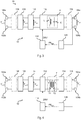
- Figure 1 shows a typical lighting system including an electronic converter 10 and at least one lighting module 20.
- a lighting module 20 includes one or more light radiation sources including e.g. at least one LED (Light Emitting Diode) or other solid-state lighting means, such as e.g. laser diodes.
- LED Light Emitting Diode
- solid-state lighting means such as e.g. laser diodes.
- the electronic converter 10 is an AC/DC electronic converter. Therefore, the electronic converter 10 includes two input terminals 102a and 102b for the connection to the mains, and two output terminals 104a and 104b for the connection to the lighting module (s) 20. Typically, line 102a is connected to phase L and terminal 102b is connected to neutral N.
- the electronic converter 10 may be either a voltage generator or a current generator.
- the lighting module 20 may be configured to be supplied with a regulated voltage or current.
- the electronic converter 10 receives at input, via terminals 102a and 102b, an alternated voltage V in,AC , such as 110 or 230 VAC, and supplies at output, via positive terminal 104a and negative terminal 104b, a regulated voltage V out , such as e.g. 12 or 24 VDC, or a regulated current i out .
- Figure 2 shows an example of a lighting module 20.
- the lighting module 20 includes a positive input terminal 200a and a negative input terminal 200b, for the connection to the terminals 104a and 104b of the electronic converter 10.
- the lighting module 20 may be connected, either directly or through a cable, to the electronic converter 10. Therefore, terminal 200a is connected to the positive terminal 104a, and terminal 200b is connected to the negative terminal 104b, and thus the lighting module 20 receives the regulated voltage V out or the regulated current i out .
- the lighting module 20 is a LED module including one or more LEDs (or laser diodes) 220, connected between the terminals 200a and 200b.
- module 20 may include a LED chain or string 22, wherein a plurality of LEDs 220 (or similarly laser diodes) are connected in series.
- the lighting module 20 is supplied with a regulated voltage
- the lighting module 20 typically includes a current regulator 24, connected in series with the LED string 22.
- the current regulator 24 may be a resistor or a linear current regulator.
- the current regulator 24 may also be implemented by current mirrors or by a switched mode current source, typically including an inductor and an electronic switch.
- a plurality of lighting modules 20 may be connected to the electronic converter 10.
- the lighting modules 20 may be connected in parallel to the terminals 104a and 104b.
- the lighting modules 20 are typically connected in series between the terminals 104a and 104b.
- Figure 3 shows the operating arrangement of an electronic converter 10.
- converter 10 includes a rectification circuit 108 and a switching stage 112.
- the input of the rectification circuit 108 such as e.g. a diode bridge, is connected (e.g. directly) to the terminals 102a and 102b. Therefore, the rectification circuit 108 receives at input the input voltage V in,AC and provides at output a DC voltage V in,DC .
- a filter circuit 106 configured to filter the noise produced by the electronic converter 10.
- a filter circuit 110 such as e.g. a capacitor connected in parallel with the output terminals of the rectification circuit 108. Therefore, in this case, the filter circuit 108 receives (e.g. directly) the voltage V in,DC and provides at output a filtered voltage, typically called a bus voltage, V bus . In this case, therefore, the switching stage 112 receives at input the voltage V bus .
- an electronic converter with power factor correction (PFC) PFC
- the switching stage 112 includes one or more electronic converters, adapted to control the flow of a current through a reactive element R.
- a reactive element R is a resonant circuit, including one or more inductive elements L, such as e.g. inductors, and one or more capacitive elements C, such as e.g. capacitors.
- the switching stage 112 is typically configured to apply an alternated voltage across said reactive circuit R.
- the switching frequency of stage 112 typically amounts to 1 kHz - 500 kHz, preferably to 20 kHz - 200 kHz.
- the electronic converter 10 is often required to be an insulated converter.
- the electronic converter 10 includes at least one transformer T, including a primary winding T1 and a secondary winding T2.
- the switching stage 112 includes one or more electronic switches, adapted to control the flow of a current through a primary winding T1 of the transformer, and the inductive element L of reactive circuit R often corresponds to the magnetizing and/or leakage inductances of transformer T.
- the reactive circuit R may include one or more inductive, L, and/or capacitive, C, elements, which are connected in series and/or in parallel with primary winding T1 and/or secondary winding T2 of the transformer. Therefore, generally speaking, transformer T may be a part of the resonant circuit R.
- the alternated voltage on the secondary side of transformer T is then converted by a rectification circuit 114, which typically includes one or more diodes (e.g. a diode bridge), into a DC voltage. Therefore, the input of the rectification circuit 114 is connected (e.g. directly) to the terminals of the secondary winding T2 of transformer T, and provides at output a DC voltage/current, which in the simplest of cases corresponds to the output voltage/current V out / i out .
- a rectification circuit 114 typically includes one or more diodes (e.g. a diode bridge)
- the input of the rectification circuit 114 is connected (e.g. directly) to the terminals of the secondary winding T2 of transformer T, and provides at output a DC voltage/current, which in the simplest of cases corresponds to the output voltage/current V out / i out .
- the switching stage 112 is driven by a control circuit 118, i.e. the control circuit 118 is configured to generate one or more drive signals DRV for driving the switching stage 112, so as to regulate the output voltage V out or the output current i out to a desired value.
- the control circuit 118 may be any analog or digital circuit, such as e.g. a microprocessor programmed via software code.
- a feedback circuit 120 is typically used to this end, and it provides a feedback signal FB REG which is determined as a function of the output voltage V out (for a voltage generator) or of the output current i out (for a current generator) .
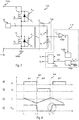
- FIGS. 5 and 6 show two examples of a switching stage 112.
- switching stage 112 receives at input, through two input terminals 112a/112b, the direct voltage V bus , wherein terminal 112b represents a reference voltage, e.g. a ground GND.
- the switching stage 112 includes a half-bridge, i.e. two electronic switches S 1 and S 2 which are connected in series between both input terminals 112a/112b, wherein the switching of the electronic switches S 1 and S 2 is driven via respective signals Q 1 and Q 2 generated by a control unit 118.
- said electronic switches S 1 are S 2 are Field-Effect Transistors (FETs), e.g. MOSFETs (Metal-Oxide-Semiconductor Field-Effect Transistors), such as e.g. n-channel FETs.
- FETs Field-Effect Transistors
- MOSFETs Metal-Oxide-Semiconductor Field-Effect Transistors
- Said switches S 1 and S 2 may be provided, in a parallel connection, with respective capacitances C A1 , C A2 (such as e.g. the parasitic capacitances of the FETs) and respective diodes D A1 , D A2 (such as e.g. the body diodes of the FETs).
- control unit 118 is configured to switch switches S 1 and S 2 alternatively, i.e. only one of the switches S 1 and S 2 is closed at a given moment.
- switch switches S 1 and S 2 alternatively, i.e. only one of the switches S 1 and S 2 is closed at a given moment.
- switches S 1 and S 2 therefore control the current flowing through the reactive element R.
- one of the switches (typically S 1 ) represents a main switch, which controls the current flowing from the input terminals 112a/112b towards the reactive element R, and the other switch (typically S 2 ) is an auxiliary switch, which typically performs the role of current freewheeling.
- the reactive element R is implemented by an inductor L and a capacitor C out .
- a first terminal of inductor L is connected to the intermediate point between both electronic switches S 1 and S 2 .
- the second terminal of inductor L is connected, via a capacitor C out , to the second input terminal 112b, thereby implementing a buck converter. Therefore, switches S 1 and S 2 may be used for selectively connecting the first terminal of inductor L to voltage V bus or to ground GND, thereby controlling the flow of current through reactive circuit R, which is comprised of inductor L and capacitor C out .
- the voltage across capacitor C out corresponds to the output voltage V out , i.e. terminal 104a is connected (e.g. directly) to the intermediate point between inductor L and capacitor C out , and terminal 104b is connected (e.g. directly) to terminal 112b.
- the inductive element L is implemented by means of a transformer T, including a primary winding T1 and a secondary winding T2.
- a transformer T may be modelled as an ideal transformer with a given winding ration 1:n, an inductance L M representing the magnetizing inductance of transformer T and an inductance L R which represents the leakage inductance, which are shown in Figure 6 on the primary side of transformer T.
- the inductive element L R may also be implemented by connecting one or more inductors in series and/or in parallel with the primary winding T1 and/or the secondary winding T2.
- a first terminal of primary winding T1 is connected to the intermediate point between both electronic switches S 1 and S 2 .
- the second terminal of primary winding T1 is connected, through a first capacitor C R1 , to the first input terminal 112a, and/or, through a second capacitor C R2 , to the second input terminal 112b / to ground GND.
- the second terminal of primary winding T1 may also be connected to a direct voltage, e.g. V bus (for example in order to implement a forward or flyback converter), or to GND.
- V bus for example in order to implement a forward or flyback converter
- switches S 1 and S 2 may be used for selectively connecting the first terminal of reactive element R (which includes the inductances of transformer T, capacitors C R1 and C R2 and optionally other inductors and/or capacitors connected in series and/or in parallel with primary winding T1 and/or with secondary winding T2) to voltage V bus or to ground GND, thereby controlling the flow of current through reactive element R.
- reactive element R which includes the inductances of transformer T, capacitors C R1 and C R2 and optionally other inductors and/or capacitors connected in series and/or in parallel with primary winding T1 and/or with secondary winding T2
- capacitor C out is typically a (large sized) capacitor which stabilizes the output voltage V out at the second terminal of inductive element L.
- capacitors C R1 and C R2 may also be sized in such a way that the reactive element R (with the inductive element L M and/or L R ) has a resonant frequency of the same order of magnitude of the switching frequency of the electronic converter, as it is the case e.g. in a LLC converter.
- switches S 1 and S 2 may be closed at zero voltage, i.e. so-called Zero Voltage Switching, ZVS.
- switch S 2 may be closed substantially at zero voltage.
- switch S 2 When switch S 2 is subsequently opened, and assuming that the current I L , which is provided by the reactive element R, is positive (i.e. the reactive element R provides a current), at this point said current I L charges capacitance C A2 and discharges capacitance C A1 , thereby increasing voltage V SW .
- the ZVS switching is typically employed in electronic converters of low to medium power. Thanks to said ZVS switching it is possible to reduce the electrical losses due to switches S 1 and S 2 . Moreover, it is possible to reduce electromagnetic emissions. As previously explained, the ZVS switching is achieved by using the energy stored in the reactive element R of switching stage 112. Said energy should therefore be controlled particularly at the moment when switch S 1 is opened and when switch S 2 is opened. For example, when the amplitude of current I L is too low at said instants, current I L may not be sufficient to charge / discharge capacitances C A1 and C A2 . On the other hand, an excessively high current might lead to a high Root Mean Square (RMS) of the current. This problem arises especially for the auxiliary switch, while the same problem is absent for the main switch, because the amplitude of current I L during the off state of the main switch is normally high.
- RMS Root Mean Square
- the present specification aims at providing solutions for controlling the operation of an electronic converter, in order to achieve a Zero Voltage Switching by resorting to a self-adjusting approach, which reduces the circulating RMS current.
- said object is achieved thanks to an electronic converter having the features set forth in the claims that follow.
- the claims also concern a corresponding lighting system and a method of operating an electronic converter.
- An electronic converter includes two input terminals, for receiving an input direct voltage, and two output terminals, for providing a regulated voltage or a regulated current.
- the electronic converter moreover includes two electronic switches, which are connected in series between both input terminals, wherein a respective capacitance is associated with each of both electronic switches, wherein one of both electronic switches represents a main switch and the other of both electronic switches represents an auxiliary switch.
- the main switch may be connected to the positive terminal and the auxiliary switch may be connected to the negative terminal, or vice-versa.
- a reactive circuit is connected between the intermediate point between both electronic switches and both output terminals.
- the reactive circuit includes at least one inductive element and at least one capacitive element.
- a control circuit is configured to drive the switching of both electronic switches via respective drive signals, wherein the control circuit is configured to drive the switching of both electronic switches in such a way as to repeat the following steps periodically:
- the electronic converter includes a measurement circuit, configured to detect a measurement signal indicative of (and preferably proportional to) the derivative of the voltage across the main switch or of the voltage across the auxiliary switch.
- the measurement circuit may be implemented by an analog differentiator which receives at input, for example, the voltage between the intermediate point between both electronic switches and the negative terminal.
- the measurement circuit may include a capacitor and one or more resistors, wherein the measurement signal corresponds to the voltage across one of the resistors.
- the duration of the fourth interval is constant, and the control circuit is configured to vary the duration of the first interval as a function of the output regulated voltage or of the output regulated current, and to vary the duration of the third interval as a function of the measurement signal.
- the duration of the second interval may be constant.
- control circuit may detect whether the energy stored in the reactive circuit is too high or too low.
- the control circuit may compare the amplitude of the measurement signal during the fourth interval with a reference value and, if the amplitude of the measurement signal exceeds the reference value during the fourth interval, the control circuit may reduce the duration of the third interval. More specifically, in various embodiments, if the amplitude of the measurement signal exceeds the reference value during the fourth interval, the control circuit may detect a value indicative of the time period between the start of the fourth interval and the instant when the measurement signal exceeds the reference value, and may verify whether said detected time period is lower than a maximum threshold. If the detected time period is lower than the maximum threshold, the control circuit may reduce the duration of the third interval.
- the control circuit may compare the amplitude of the measurement signal during the first interval with a reference value and, if the amplitude of the measurement signal exceeds the reference value during the first interval, it may increase the duration of the third interval.
- control circuit may also directly detect the maximum amplitude of the measurement signal during the fourth interval, and vary the duration of the third interval, so that the maximum amplitude corresponds to a reference value.
- control circuit may vary the duration of the third interval, such that the maximum amplitude remains between a lower limit and an upper limit.
- FIG 7 shows a first embodiment of a switching stage 112' for an electronic converter according to the present specification.
- a switching stage 112 may be used in the electronic converters described with reference to Figures 1 to 6 , and the description thereof applies in its entirety.
- the switching stage 112' again includes at least two switches S 1 and S 2 , which are connected (e.g. directly) between two terminals 112a and 112b, configured to receive voltage V bus (see also Figures 3 and 4 ).
- the intermediate point between both switches S 1 and S 2 is connected to a first terminal of a reactive circuit R, in such a way as to control the flow of current through reactive circuit R.
- the specific implementation of the reactive element R (inductor L and/or transformer T, and one or more capacitors) and the connection of the other terminals of reactive circuit R are not particularly relevant for the operation of the Zero Voltage Switching which constitutes the object of the present specification.
- the reactive circuit R is interposed between the output of the electronic converter and the intermediate point between switches S 1 and S 2 , and switches S 1 and S 2 may be used for controlling the flow of current through the reactive circuit R, thereby controlling the energy transfer towards outputs 104a and 104b of the electronic converter.
- switches S 1 and S 2 may be used for controlling the flow of current through the reactive circuit R, thereby controlling the energy transfer towards outputs 104a and 104b of the electronic converter.
- Figures 5 and 6 for exemplary switching stages 112.
- the switching stage 112' should be sized so that, when switch S 1 is opened, the energy stored in the reactive element R is sufficient to discharge capacitance C A2 and to charge capacitance C A1 until voltage V SW is substantially zero.
- switch S 2 when switch S 2 is opened, the energy stored in the reactive element R should be sufficient to charge capacitance C A2 and to discharge capacitance C A1 until voltage V SW is substantially V bus .
- One of the switches S 1 and S 2 often corresponds to a main switch, which controls the flow of energy towards outputs 104a and 104b.
- the other switch is typically only an auxiliary switch, which enables achieving the ZVS condition for the main switch.
- the main switch is switch S 1 and the auxiliary switch is switch S 2 .
- the main switch is switch S 1 and the auxiliary switch is switch S 2 .
- the function of both switches may be reversed, e.g. by reversing the connection of secondary winding T2. Therefore, typically, the control circuit 118' varies the duration of the closed state of the main switch, in order to control the output voltage V out or the output current i out .
- the energy stored in the reactive element R is high and sufficient to charge the capacitance (C A1 or C A2 ) associated with the main switch, and to discharge the capacitance (C A1 or C A2 ) associated with the auxiliary switch.
- an additional control is required to control the instant when the auxiliary switch is opened, because the energy stored in the reactive element R is typically low at that instant.
- control unit 118' may implement a ZVS by measuring said current I L .
- this current measurement generates electrical losses.
- an alternative solution involves detecting the ZVS condition through a direct measurement of voltage V SW .
- the electronic converter includes a measurement circuit 122, such as for example an analog differentiator, configured to detect a measurement signal indicative of the derivative of the voltage across the main switch, e.g. a measurement signal which is proportional to the derivative of said voltage, and the control circuit 118' is configured to vary the duration of the closed state of the auxiliary switch as a function of the measurement signal.
- a measurement circuit 122 such as for example an analog differentiator, configured to detect a measurement signal indicative of the derivative of the voltage across the main switch, e.g. a measurement signal which is proportional to the derivative of said voltage
- the control circuit 118' is configured to vary the duration of the closed state of the auxiliary switch as a function of the measurement signal.
- the switching stage 112' includes:
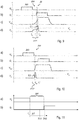
- FIG. 8 shows an embodiment of the driving performed by control circuit 118'.
- control circuit 118' is configured to repeat the following steps periodically:
- This driving arrangement may be applied irrespective of which switch, S 1 or S 2 , is the main switch or the auxiliary switch.
- the main switch is switch S 1 and the auxiliary switch is switch S 2 .
- the control circuit 118' opens switch S 1 at an instant t 2 . Therefore, during interval ⁇ t2 , the intermediate point between the switches is not connected to a direct voltage. However, in this case, the capacitances C A1 and C A2 are connected to the reactive circuit R. Specifically, in the presently considered embodiment, it is assumed that the current I L provided by reactive circuit R is negative at instant t 2 (i.e., the reactive circuit R absorbs energy). As a consequence, capacitance C A2 is discharged and capacitance C A1 is charged, i.e. voltage V SW decreases.
- control circuit 118' opens switch S 2 at an instant t 4 . Therefore, during interval ⁇ t3 , the intermediate point between the switches is not connected to a direct voltage, and the capacitances C A1 and C A2 are again connected to the reactive circuit R 2 .
- the current I L provided by the reactive circuit is positive at instant t 4 (i.e. the reactive circuit R provides energy).
- capacitance C A2 is charged and capacitance C A1 is discharged, i.e. voltage V SW increases.
- one of the switches is a main switch (e.g. switch S 1 ) and the other switch is an auxiliary switch (e.g. switch S 2 ).
- the control circuit 118' is configured to vary the duration of the interval during which the main switch is closed ( ⁇ t1 in the exemplary case), so as to achieve a required output voltage V out or output current i out .
- control circuit 118' is configured to vary the duration of the interval during which the auxiliary switch is closed ( ⁇ t3 in the exemplary case), so as to create the ZVS condition for the switching of the main switch.
- the control circuit 118' includes a circuit 1184 configured to determine a first signal indicative of said duration (e.g. ⁇ t1 ) as a function of the output voltage V out or the output current i out and a reference signal REF.
- circuit 1184 may be a regulator with an integral (I) component and optionally, in addition, with a proportional (P) and/or derivative (D) component.
- the first signal is then forwarded to a driver circuit 1186, which generates the drive signals Q 1 and Q 2 for switches S 1 and S 2 .
- the present specification mainly concerns the driving of the auxiliary switch, specifically the duration of interval ( ⁇ t3 ) during which the auxiliary switch is closed, and the duration of the following interval ( ⁇ t4 ) during which both switches are opened.
- the duration of interval ( ⁇ t4 ) between the instant ( t 4 ) when the auxiliary switch is opened and the instant ( t 1 ' ) wherein the main switch is closed is constant, and the control circuit regulates the duration of interval ( ⁇ t3 ) during which the auxiliary switch is closed.
- the duration of interval ( ⁇ t2 ) between the instant ( t 2 ) when the main switch is opened and the instant ( t 3 ) when the auxiliary switch is closed is not particularly relevant, and said duration may be e.g. constant.
- the electronic converter includes, to this end, a measurement circuit 122, configured to generate a signal V D indicative of the derivative of voltage V SW at the intermediate point between switches S 1 and S 2 .
- the measurement circuit 122 is connected between the intermediate point between switches S 1 and S 2 and a reference voltage, e.g. terminal 102a or terminal 102b. Therefore, in various embodiments, the measurement circuit 122 is configured to generate a signal V D indicative of the derivative of the voltage across switch S 1 or switch S 2 . Preferably, the measurement circuit is connected across switch S 2 , because said switch is connected to ground GND.
- the measurement circuit 122 includes a capacitor C 1 and at least one resistor connected in series. Therefore, capacitor C 1 generates a current which is proportional to the derivative of voltage V SW , and the resistor generates a voltage which is proportional to said current.
- capacitor C 1 generates a current which is proportional to the derivative of voltage V SW
- resistor generates a voltage which is proportional to said current.
- resistors R 1 and R 2 are used, and they implement a voltage divider.
- a first terminal of capacitor C 1 is connected (e.g. directly) to the intermediate point between switches S 1 and S 2 .
- voltage V D corresponds to the derivative of voltage V SW , filtered by a low-pass filter.
- resistor R 1 a resistance which is much higher than the resistance for resistor R 2 (for example R 1 > 5 x R 2 )
- the time constant of the filter is mainly determined by the resistance of resistor R 1 , while resistor R 2 and capacitor C control the derivation coefficient.
- control circuit 118' should therefore monitor:
- control circuit 118' is configured to compare signal V D with at least one reference threshold V th .
- control circuit may detect whether the amplitude (absolute value) of signal V D exceeds threshold V th , which indicates a strong variation of voltage V SW .
- the first instance is shown in Figure 9 .
- the main switch (S 1 in the presently considered exemplary instance) is closed at instant t 1 , not at zero voltage.
- the control circuit 118' generates the drive signal for the auxiliary switch in such a way as to open the auxiliary switch after a variable duration ( ⁇ t3 in the exemplary instance) and subsequently closes the main switch after a constant duration ( ⁇ t4 for the exemplary instance). If the voltage across the main switch is not zero, e.g. voltage V SW is lower than V bus for the exemplary instance, closing the main switch therefore strongly varies voltage V SW (see Figure 9c ).
- the voltage across the main switch is not zero at instant t E1 , i.e. voltage V SW is lower than voltage V bus .
- the voltage across the main switch undergoes, at instant t E1 , a strong variation, i.e. the value of signal V D is high.
- the second instance is shown in Figure 10 . Specifically, in this instance, the energy stored in the reactive circuit R and provided to capacitances C A1 and C A2 is too high.
- the control circuit 118' may detect, at an instant t E2 , a second event E2 when signal V D exceeds threshold V th , wherein said instant (with reference to the start of interval ⁇ t4 ) occurs after a time period ⁇ T2 , wherein ⁇ T2 ⁇ ⁇ t4 .
- a first event E1 only occurs if voltage V D includes a strong variation at an instant t E1 which takes place after the end of interval ⁇ t4 .
- a second event E2 occurs if voltage V D includes a strong variation at an instant t E2 during interval ⁇ t4 , typically at the start of interval ⁇ t4 .
- the control circuit 118' may therefore be configured to verify if voltage V D includes a strong variation.
- the control circuit 118' may detect a strong variation by comparing voltage V D with a reference voltage V th .
- the control circuit 118' includes a comparator 1180, which is configured to generate a comparison signal E by verifying whether voltage V D is higher than reference voltage V th .
- comparator 1180 is an analog comparator.
- the control circuit 118' may also compare voltage V D with a first reference voltage V th1 during interval ⁇ t4 , and with a second reference voltage V th2 after the end of interval ⁇ t4 .
- control circuit 118' may verify if the instant when reference voltage V D reaches or exceeds reference voltage V th is indicative of an event of the first type E1 or of the second type E2. For example, to this end the control circuit 118' may verify whether the instant when voltage V D reaches or exceeds reference voltage V th is before or after instant t 1 ' , and may classify the event as E1 or E2, respectively. As an alternative, the control circuit 118' may also detect the time elapsed from instant t 4 (end of interval ⁇ t3 / start of interval ⁇ t4 ), and compare said time period with one or more thresholds.
- the measurement circuit 122 and/or the threshold V th are suitably sized so that signal V D does not exceed threshold V th when the voltage variation across the main switch is lower than a maximum value, which however enables discharging the capacitance associated with the main switch. Therefore, in this instance, the control circuit 118' may include a processing circuit 1182, configured to detect:
- the processing circuit 1182 may be configured to determine the time ⁇ T which has elapsed from the start of interval t4 until voltage V D reaches or exceeds reference voltage V th (shown for example by a rising edge of signal E ). Subsequently, the processing circuit 1182 may detect:
- threshold TH2 is chosen between duration ⁇ t4 and duration ⁇ t4 + ⁇ t , i.e. threshold TH2 substantially corresponds to duration ⁇ t4 .
- threshold TH1 is lower than duration ⁇ t4 , for example between 30% and 90% of duration ⁇ t4 , preferably between 50% and 70% of duration ⁇ t4 .
- the processing circuit 1182 may provide a control signal indicative of the duration of the closed state for the auxiliary switch (e.g. ⁇ t3 ) to the driver circuit 1186, which generates the drive signals Q 1 and Q 2 .
- the processing circuit 1182 may keep unvaried the duration of the interval during which the auxiliary switch is closed when no event is detected, for example when the (absolute) variation of voltage V SW stays below threshold V th .
- the driver circuit 1182 should perform operations which differ for an event E1 and for an event E2.
- the first event EI indicates that the energy provided by reactive element R was not sufficient, because the main switch does not close at zero voltage. Typically, this takes place when the duration of the interval during which the auxiliary switch is closed ( ⁇ t3 ) was not sufficiently long. Therefore, in various embodiments, in response to said event E1, the processing circuit 1182 increases the duration of said interval.
- the second event E2 indicates that the energy provided by reactive element R was excessive, because the ZVS condition for the main switch is reached too rapidly, i.e. at the start of interval ⁇ t4 . Typically, this takes place when the duration of the interval during which the auxiliary switch is closed ( ⁇ t3 ) was too long. Therefore, in various embodiments, in response to said event E2, the processing circuit 1182 reduces the duration of said interval.
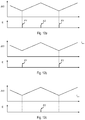
- Figures 12a, 12b and 12c show some possible control arrangements for varying the duration during which the auxiliary switch is closed ( ⁇ t3 in the exemplary case).
- the processing circuit 1182 may lower the duration of the interval during which the auxiliary switch is closed ( ⁇ t3 in the exemplary case) until an event E1 is detected, indicating that the main switch does not close at zero voltage. Therefore, in response to said event E1, the processing circuit 1182 may increase the duration of the interval during which the auxiliary switch is closed until an event E2 is detected, indicating that the capacitance associated to the main switch is discharged too rapidly. Therefore, in response to said event E2, the processing circuit 1182 may reduce the duration of the interval during which the auxiliary switch is closed. For example, in the presently considered embodiment, the processing circuit 1182 varies time linearly.
- processing circuit 1182 may also monitor only one of the events E1 or E2.
- the driver circuit 1182 may perform one of the following operations:
- the processing circuit 1182 determines said maximum value t max by adding a constant value ⁇ tmax to the value of duration ⁇ t3 when event E1 is detected.
- the processing circuit 1182 progressively reduces the duration of the interval, until a new event E1 is detected.
- the processing circuit 1182 may perform one of the following operations:
- the driver circuit 1182 may determine said minimum value by subtracting a constant value ⁇ tmin from the value of duration ⁇ t3 when event E2 is detected.
- the processing circuit 1182 progressively increases the duration of the interval, until a new event E2 is detected.
- control circuit 118' is configured to:
- the control circuit 118' substantially detects if the energy stored in the reactive element R shortly before the off switching of the auxiliary switch remains within given limits (i.e. it is neither too low, which would generate an event E1, nor too high, which would generate an event E2).
- Figure 13 shows an alternative embodiment of a processing circuit 1182', which is configured to directly regulate the duration of the interval during which the auxiliary switch is closed ( ⁇ t3 ) as a function of the maximum variation of voltage V SW (or similarly the voltage of the main or of the auxiliary switch), or as a function of the maximum amplitude of signal V D , in the interval ( ⁇ t4 ) before closing the main switch.
- signal V D is provided to a sample-and-hold circuit 1190, configured to store a signal indicative of the maximum value of voltage V D during the interval before closing the main switch (e.g. ⁇ t4 ).
- circuit 1190 is implemented by a capacitor C P and a diode D P , which transfers voltage V D to capacitor C P when voltage V D is higher than voltage V DP across capacitor C P . Therefore, capacitor C P represents an analog memory, which stores the maximum value of voltage V D .
- a resistor R P may be connected in parallel to capacitor C P , in such a way as to progressively discharge capacitor C P .
- the maximum detected value i.e. voltage V DP
- V DP the maximum detected value
- the processing circuit 1182' configured to generate the signal indicative of the duration of interval ⁇ t3 , i.e. of the duration of the interval during which the auxiliary switch is closed.
- the processing circuit 1182' determines the value for the duration ⁇ t3 (in the exemplary case) always at the same instant, e.g. at instant t 1 when the main switch is closed.
- the processing circuit 1182' is configured to determine the value of the duration of interval ⁇ t3 , i.e. of the interval during which the auxiliary switch is closed, as a function of the peak voltage V DP .
- the processing circuit 1182' is configured to compare the detected value V DP with a lower threshold and with a higher threshold, and to vary the duration of the interval during which the auxiliary switch is closed, so as to keep the value between said thresholds.
- the processing circuit 1182' implements a regulator, configured to regulate the duration of the interval during which the auxiliary switch is closed as a function of the maximum detected variation, i.e. as a function of signal V DP .
- said signal indicative of the required duration of interval ⁇ t3 is therefore provided to the driver circuit 1186 of switches S 1 and S 2 , which in the presently considered embodiment drives the auxiliary switch S 2 correspondingly, i.e. by generating a pulse, wherein the on duration corresponds to the required duration.
- value V DP is provided to a summing node 1192, configured to calculate the difference between value V DP and a required value V ref .
- a regulator 1194 which includes at least an I component, such as e.g. a PI (Proportional-Integral) regulator, varies the signal indicative of the duration of interval ⁇ t3 until the difference is zero, i.e. until value V DP corresponds to the required value V ref .
- I component such as e.g. a PI (Proportional-Integral) regulator
- sample-and-hold circuit / the peak value detector 1190, and especially regulator 1192 and/or driver circuit 1186 may also be implemented by a digital circuit, such as e.g. a microprocessor programmed via software code.
- the measurement circuit 1190 described in the foregoing may therefore be applied across switch S 1 .
- the measurement circuit 122 may monitor voltage V SW across switch S 2 , specifically the negative variations during interval ⁇ t2 , instead of the positive variations during interval ⁇ t4 as described in the foregoing.
- the variation frequency of the duration of the interval during which the auxiliary switch is closed may be low as compared to the switching frequency of the switching stage, therefore avoiding an influence on the main control loop by the interval during which the main switch is closed.
- the measurement circuit 122 does not require a high accuracy, because it is sufficient to avoid the events E1 and E2 described in the foregoing (or at least to reduce the number of said events).
Applications Claiming Priority (1)
| Application Number | Priority Date | Filing Date | Title |
|---|---|---|---|
| IT201800008950 | 2018-09-26 |
Publications (2)
| Publication Number | Publication Date |
|---|---|
| EP3629462A1 true EP3629462A1 (de) | 2020-04-01 |
| EP3629462B1 EP3629462B1 (de) | 2023-11-08 |
Family
ID=64607200
Family Applications (1)
| Application Number | Title | Priority Date | Filing Date |
|---|---|---|---|
| EP19199182.7A Active EP3629462B1 (de) | 2018-09-26 | 2019-09-24 | Elektronischer umrichter und zugehöriges beleuchtungssystem und verfahren zum betrieb eines elektronischen umrichters |
Country Status (1)
| Country | Link |
|---|---|
| EP (1) | EP3629462B1 (de) |
Cited By (2)
| Publication number | Priority date | Publication date | Assignee | Title |
|---|---|---|---|---|
| IT201900025132A1 (it) * | 2019-12-20 | 2021-06-20 | St Microelectronics Srl | Circuito generatore di impulsi, relativo sistema laser e procedimento |
| US11894657B2 (en) | 2020-07-07 | 2024-02-06 | Stmicroelectronics S.R.L. | Pulse generator circuit, related system and method |
Citations (5)
| Publication number | Priority date | Publication date | Assignee | Title |
|---|---|---|---|---|
| US7450404B2 (en) | 2005-10-31 | 2008-11-11 | Delta Electronics, Inc. | Switching power supply and ZVS method thereof |
| US20120105039A1 (en) * | 2010-10-29 | 2012-05-03 | R2 Semiconductor, Inc. | Delay Block for Controlling a Dead Time of a Switching Voltage Regulator |
| US20140312868A1 (en) * | 2013-04-23 | 2014-10-23 | Nvidia Corporation | Control of a soft-switched variable frequency multi-phase regulator |
| US20160141960A1 (en) | 2014-11-19 | 2016-05-19 | Futurewei Technologies, Inc. | Zero Voltage Switching Detection Apparatus and Method |
| EP3217525A1 (de) * | 2016-03-09 | 2017-09-13 | Grundfos Holding A/S | Steuerungsverfahren zur steuerung eines stromrichterschaltung und entsprechende stromrichterschaltung |
-
2019
- 2019-09-24 EP EP19199182.7A patent/EP3629462B1/de active Active
Patent Citations (5)
| Publication number | Priority date | Publication date | Assignee | Title |
|---|---|---|---|---|
| US7450404B2 (en) | 2005-10-31 | 2008-11-11 | Delta Electronics, Inc. | Switching power supply and ZVS method thereof |
| US20120105039A1 (en) * | 2010-10-29 | 2012-05-03 | R2 Semiconductor, Inc. | Delay Block for Controlling a Dead Time of a Switching Voltage Regulator |
| US20140312868A1 (en) * | 2013-04-23 | 2014-10-23 | Nvidia Corporation | Control of a soft-switched variable frequency multi-phase regulator |
| US20160141960A1 (en) | 2014-11-19 | 2016-05-19 | Futurewei Technologies, Inc. | Zero Voltage Switching Detection Apparatus and Method |
| EP3217525A1 (de) * | 2016-03-09 | 2017-09-13 | Grundfos Holding A/S | Steuerungsverfahren zur steuerung eines stromrichterschaltung und entsprechende stromrichterschaltung |
Non-Patent Citations (2)
| Title |
|---|
| "Zero Voltage Switching Resonant Power Conversion", TEXAS INSTRUMENTS, 1999 |
| L. WUIDART: "Application Note - Topologies For Switched Mode Power Supplies", STMICROELECTRONICS, 1999 |
Cited By (2)
| Publication number | Priority date | Publication date | Assignee | Title |
|---|---|---|---|---|
| IT201900025132A1 (it) * | 2019-12-20 | 2021-06-20 | St Microelectronics Srl | Circuito generatore di impulsi, relativo sistema laser e procedimento |
| US11894657B2 (en) | 2020-07-07 | 2024-02-06 | Stmicroelectronics S.R.L. | Pulse generator circuit, related system and method |
Also Published As
| Publication number | Publication date |
|---|---|
| EP3629462B1 (de) | 2023-11-08 |
Similar Documents
| Publication | Publication Date | Title |
|---|---|---|
| CN109247081B (zh) | 半桥谐振转换器、使用它们的电路、以及对应的控制方法 | |
| EP2536013B1 (de) | Aufwärts- und Abwärtswandler in Kaskade | |
| US8305004B2 (en) | Apparatus and method for constant power offline LED driver | |
| US10020742B2 (en) | Hybrid boost-bypass function in two-stage converter | |
| CN109247042B (zh) | Ac/dc pfc转换器、转换方法和led驱动器 | |
| US8130520B2 (en) | Power supply apparatus and semiconductor integrated circuit device | |
| US7525293B1 (en) | Power supply switching circuit for a halogen lamp | |
| EP2248249B1 (de) | Elektronische treiberschaltung und verfahren | |
| US20120293141A1 (en) | Bridgeless pfc converter and the method thereof | |
| EP3050400B1 (de) | Elektronischer resonanter und isolierter zeta-halbbrückenwandler samt steuerverfahren | |
| EP3414824B1 (de) | Gleichstromresonanzwandler und leistungsfaktorkorrektur mit resonanzwandlern sowie entsprechende steuerungsverfahren | |
| US9444246B2 (en) | Power converter with switching element | |
| EP3414821A1 (de) | Gleichstromresonanzwandler und leistungsfaktorkorrektur mithilfe von resonanzwandlern sowie zugehörige steuerungsverfahren | |
| EP3186877B1 (de) | Schwebender boost-buck-ausgangsspannungsregler mit einem buck-steuergerät mit niedriger eingangs- und niedriger ausgangswelligkeit | |
| CN103259397A (zh) | 开关电源装置 | |
| WO2015135073A1 (en) | Primary side controlled led driver with ripple cancellation | |
| EP3629462B1 (de) | Elektronischer umrichter und zugehöriges beleuchtungssystem und verfahren zum betrieb eines elektronischen umrichters | |
| EP3365967B1 (de) | Elektronischer wandler und zugehöriges verfahren zum betrieb eines elektronischen wandlers | |
| EP3327915A1 (de) | Elektronischer wandler und zugehöriges verfahren zum betrieb eines elektronischen wandlers | |
| US9078317B1 (en) | Floating output voltage boost regulator driving LEDs using a buck controller | |
| KR101796431B1 (ko) | 역률 보상형 led 구동장치 및 구동방법 | |
| EP3528378B1 (de) | Elektronischer wandler und zugehöriges beleuchtungssystem | |
| KR100946437B1 (ko) | 저손실 대기모드를 갖는 스위칭 전원장치 | |
| EP3402060B1 (de) | Elektronischer wandler und zugehöriges verfahren zum betrieb eines elektronischen wandlers | |
| WO2017137342A1 (en) | Dc/dc resonant converters and power factor correction using resonant converters, and corresponding control methods |
Legal Events
| Date | Code | Title | Description |
|---|---|---|---|
| PUAI | Public reference made under article 153(3) epc to a published international application that has entered the european phase |
Free format text: ORIGINAL CODE: 0009012 |
|
| STAA | Information on the status of an ep patent application or granted ep patent |
Free format text: STATUS: THE APPLICATION HAS BEEN PUBLISHED |
|
| AK | Designated contracting states |
Kind code of ref document: A1 Designated state(s): AL AT BE BG CH CY CZ DE DK EE ES FI FR GB GR HR HU IE IS IT LI LT LU LV MC MK MT NL NO PL PT RO RS SE SI SK SM TR |
|
| AX | Request for extension of the european patent |
Extension state: BA ME |
|
| STAA | Information on the status of an ep patent application or granted ep patent |
Free format text: STATUS: REQUEST FOR EXAMINATION WAS MADE |
|
| 17P | Request for examination filed |
Effective date: 20200916 |
|
| RBV | Designated contracting states (corrected) |
Designated state(s): AL AT BE BG CH CY CZ DE DK EE ES FI FR GB GR HR HU IE IS IT LI LT LU LV MC MK MT NL NO PL PT RO RS SE SI SK SM TR |
|
| RAP1 | Party data changed (applicant data changed or rights of an application transferred) |
Owner name: OSRAM S.P.A. - SOCIETA' RIUNITE OSRAM EDISON CLERICI Owner name: OSRAM GMBH |
|
| RAP3 | Party data changed (applicant data changed or rights of an application transferred) |
Owner name: OSRAM GMBH Owner name: OSRAM S.P.A. - SOCIETA' RIUNITE OSRAM EDISON CLERICI |
|
| RIC1 | Information provided on ipc code assigned before grant |
Ipc: H02M 1/00 20060101ALN20210730BHEP Ipc: H02M 3/337 20060101ALI20210730BHEP Ipc: H02M 3/158 20060101AFI20210730BHEP |
|
| RIC1 | Information provided on ipc code assigned before grant |
Ipc: H02M 1/00 20060101ALN20210825BHEP Ipc: H02M 3/337 20060101ALI20210825BHEP Ipc: H02M 3/158 20060101AFI20210825BHEP |
|
| GRAP | Despatch of communication of intention to grant a patent |
Free format text: ORIGINAL CODE: EPIDOSNIGR1 |
|
| STAA | Information on the status of an ep patent application or granted ep patent |
Free format text: STATUS: GRANT OF PATENT IS INTENDED |
|
| INTG | Intention to grant announced |
Effective date: 20211001 |
|
| GRAJ | Information related to disapproval of communication of intention to grant by the applicant or resumption of examination proceedings by the epo deleted |
Free format text: ORIGINAL CODE: EPIDOSDIGR1 |
|
| STAA | Information on the status of an ep patent application or granted ep patent |
Free format text: STATUS: REQUEST FOR EXAMINATION WAS MADE |
|
| STAA | Information on the status of an ep patent application or granted ep patent |
Free format text: STATUS: EXAMINATION IS IN PROGRESS |
|
| INTC | Intention to grant announced (deleted) | ||
| 17Q | First examination report despatched |
Effective date: 20220224 |
|
| RAP1 | Party data changed (applicant data changed or rights of an application transferred) |
Owner name: OSRAM S.P.A. - SOCIETA' RIUNITE OSRAM EDISON CLERICI Owner name: OPTOTRONIC GMBH |
|
| GRAP | Despatch of communication of intention to grant a patent |
Free format text: ORIGINAL CODE: EPIDOSNIGR1 |
|
| STAA | Information on the status of an ep patent application or granted ep patent |
Free format text: STATUS: GRANT OF PATENT IS INTENDED |
|
| RIC1 | Information provided on ipc code assigned before grant |
Ipc: H02M 1/00 20060101ALN20230630BHEP Ipc: H02M 3/337 20060101ALI20230630BHEP Ipc: H02M 3/158 20060101AFI20230630BHEP |
|
| INTG | Intention to grant announced |
Effective date: 20230717 |
|
| RAP1 | Party data changed (applicant data changed or rights of an application transferred) |
Owner name: OPTOTRONIC GMBH |
|
| RAP3 | Party data changed (applicant data changed or rights of an application transferred) |
Owner name: INVENTRONICS GMBH |
|
| GRAS | Grant fee paid |
Free format text: ORIGINAL CODE: EPIDOSNIGR3 |
|
| GRAA | (expected) grant |
Free format text: ORIGINAL CODE: 0009210 |
|
| STAA | Information on the status of an ep patent application or granted ep patent |
Free format text: STATUS: THE PATENT HAS BEEN GRANTED |
|
| AK | Designated contracting states |
Kind code of ref document: B1 Designated state(s): AL AT BE BG CH CY CZ DE DK EE ES FI FR GB GR HR HU IE IS IT LI LT LU LV MC MK MT NL NO PL PT RO RS SE SI SK SM TR |
|
| REG | Reference to a national code |
Ref country code: GB Ref legal event code: FG4D |
|
| REG | Reference to a national code |
Ref country code: CH Ref legal event code: EP |
|
| REG | Reference to a national code |
Ref country code: DE Ref legal event code: R096 Ref document number: 602019040961 Country of ref document: DE |
|
| REG | Reference to a national code |
Ref country code: IE Ref legal event code: FG4D |
|
| REG | Reference to a national code |
Ref country code: LT Ref legal event code: MG9D |
|
| REG | Reference to a national code |
Ref country code: NL Ref legal event code: MP Effective date: 20231108 |
|
| PG25 | Lapsed in a contracting state [announced via postgrant information from national office to epo] |
Ref country code: GR Free format text: LAPSE BECAUSE OF FAILURE TO SUBMIT A TRANSLATION OF THE DESCRIPTION OR TO PAY THE FEE WITHIN THE PRESCRIBED TIME-LIMIT Effective date: 20240209 |
|
| PG25 | Lapsed in a contracting state [announced via postgrant information from national office to epo] |
Ref country code: IS Free format text: LAPSE BECAUSE OF FAILURE TO SUBMIT A TRANSLATION OF THE DESCRIPTION OR TO PAY THE FEE WITHIN THE PRESCRIBED TIME-LIMIT Effective date: 20240308 |
|
| PG25 | Lapsed in a contracting state [announced via postgrant information from national office to epo] |
Ref country code: LT Free format text: LAPSE BECAUSE OF FAILURE TO SUBMIT A TRANSLATION OF THE DESCRIPTION OR TO PAY THE FEE WITHIN THE PRESCRIBED TIME-LIMIT Effective date: 20231108 |
|
| REG | Reference to a national code |
Ref country code: AT Ref legal event code: MK05 Ref document number: 1630527 Country of ref document: AT Kind code of ref document: T Effective date: 20231108 |
|
| PG25 | Lapsed in a contracting state [announced via postgrant information from national office to epo] |
Ref country code: NL Free format text: LAPSE BECAUSE OF FAILURE TO SUBMIT A TRANSLATION OF THE DESCRIPTION OR TO PAY THE FEE WITHIN THE PRESCRIBED TIME-LIMIT Effective date: 20231108 |
|
| PG25 | Lapsed in a contracting state [announced via postgrant information from national office to epo] |
Ref country code: AT Free format text: LAPSE BECAUSE OF FAILURE TO SUBMIT A TRANSLATION OF THE DESCRIPTION OR TO PAY THE FEE WITHIN THE PRESCRIBED TIME-LIMIT Effective date: 20231108 |
|
| PG25 | Lapsed in a contracting state [announced via postgrant information from national office to epo] |
Ref country code: ES Free format text: LAPSE BECAUSE OF FAILURE TO SUBMIT A TRANSLATION OF THE DESCRIPTION OR TO PAY THE FEE WITHIN THE PRESCRIBED TIME-LIMIT Effective date: 20231108 |
|
| PG25 | Lapsed in a contracting state [announced via postgrant information from national office to epo] |
Ref country code: NL Free format text: LAPSE BECAUSE OF FAILURE TO SUBMIT A TRANSLATION OF THE DESCRIPTION OR TO PAY THE FEE WITHIN THE PRESCRIBED TIME-LIMIT Effective date: 20231108 Ref country code: LT Free format text: LAPSE BECAUSE OF FAILURE TO SUBMIT A TRANSLATION OF THE DESCRIPTION OR TO PAY THE FEE WITHIN THE PRESCRIBED TIME-LIMIT Effective date: 20231108 Ref country code: IS Free format text: LAPSE BECAUSE OF FAILURE TO SUBMIT A TRANSLATION OF THE DESCRIPTION OR TO PAY THE FEE WITHIN THE PRESCRIBED TIME-LIMIT Effective date: 20240308 Ref country code: GR Free format text: LAPSE BECAUSE OF FAILURE TO SUBMIT A TRANSLATION OF THE DESCRIPTION OR TO PAY THE FEE WITHIN THE PRESCRIBED TIME-LIMIT Effective date: 20240209 Ref country code: ES Free format text: LAPSE BECAUSE OF FAILURE TO SUBMIT A TRANSLATION OF THE DESCRIPTION OR TO PAY THE FEE WITHIN THE PRESCRIBED TIME-LIMIT Effective date: 20231108 Ref country code: BG Free format text: LAPSE BECAUSE OF FAILURE TO SUBMIT A TRANSLATION OF THE DESCRIPTION OR TO PAY THE FEE WITHIN THE PRESCRIBED TIME-LIMIT Effective date: 20240208 Ref country code: AT Free format text: LAPSE BECAUSE OF FAILURE TO SUBMIT A TRANSLATION OF THE DESCRIPTION OR TO PAY THE FEE WITHIN THE PRESCRIBED TIME-LIMIT Effective date: 20231108 Ref country code: PT Free format text: LAPSE BECAUSE OF FAILURE TO SUBMIT A TRANSLATION OF THE DESCRIPTION OR TO PAY THE FEE WITHIN THE PRESCRIBED TIME-LIMIT Effective date: 20240308 |