EP3629379A1 - Ga2o3-based semiconductor device - Google Patents
Ga2o3-based semiconductor device Download PDFInfo
- Publication number
- EP3629379A1 EP3629379A1 EP18790539.3A EP18790539A EP3629379A1 EP 3629379 A1 EP3629379 A1 EP 3629379A1 EP 18790539 A EP18790539 A EP 18790539A EP 3629379 A1 EP3629379 A1 EP 3629379A1
- Authority
- EP
- European Patent Office
- Prior art keywords
- crystal layer
- based crystal
- doped
- region
- concentration
- Prior art date
- Legal status (The legal status is an assumption and is not a legal conclusion. Google has not performed a legal analysis and makes no representation as to the accuracy of the status listed.)
- Pending
Links
- 239000004065 semiconductor Substances 0.000 title claims abstract description 32
- 239000013078 crystal Substances 0.000 claims abstract description 256
- QZQVBEXLDFYHSR-UHFFFAOYSA-N gallium(III) oxide Inorganic materials O=[Ga]O[Ga]=O QZQVBEXLDFYHSR-UHFFFAOYSA-N 0.000 claims description 271
- 230000004888 barrier function Effects 0.000 claims description 32
- 230000000903 blocking effect Effects 0.000 claims description 7
- 239000007789 gas Substances 0.000 description 30
- 238000005468 ion implantation Methods 0.000 description 18
- 239000000758 substrate Substances 0.000 description 18
- 239000000203 mixture Substances 0.000 description 14
- 229910021480 group 4 element Inorganic materials 0.000 description 9
- 229910052718 tin Inorganic materials 0.000 description 9
- 239000002019 doping agent Substances 0.000 description 7
- 239000012535 impurity Substances 0.000 description 7
- VYPSYNLAJGMNEJ-UHFFFAOYSA-N Silicium dioxide Chemical compound O=[Si]=O VYPSYNLAJGMNEJ-UHFFFAOYSA-N 0.000 description 5
- 238000001004 secondary ion mass spectrometry Methods 0.000 description 5
- 238000000137 annealing Methods 0.000 description 4
- CBENFWSGALASAD-UHFFFAOYSA-N Ozone Chemical compound [O-][O+]=O CBENFWSGALASAD-UHFFFAOYSA-N 0.000 description 3
- 229910052681 coesite Inorganic materials 0.000 description 3
- 229910052906 cristobalite Inorganic materials 0.000 description 3
- 238000002474 experimental method Methods 0.000 description 3
- 230000005669 field effect Effects 0.000 description 3
- 238000000034 method Methods 0.000 description 3
- 238000001451 molecular beam epitaxy Methods 0.000 description 3
- IJGRMHOSHXDMSA-UHFFFAOYSA-N nitrogen Substances N#N IJGRMHOSHXDMSA-UHFFFAOYSA-N 0.000 description 3
- 229910052682 stishovite Inorganic materials 0.000 description 3
- 229910052905 tridymite Inorganic materials 0.000 description 3
- 229910052782 aluminium Inorganic materials 0.000 description 2
- 230000007423 decrease Effects 0.000 description 2
- 230000000694 effects Effects 0.000 description 2
- 230000005684 electric field Effects 0.000 description 2
- 229910052738 indium Inorganic materials 0.000 description 2
- 239000011810 insulating material Substances 0.000 description 2
- 229910052751 metal Inorganic materials 0.000 description 2
- 239000002184 metal Substances 0.000 description 2
- 229910052757 nitrogen Inorganic materials 0.000 description 2
- 239000012299 nitrogen atmosphere Substances 0.000 description 2
- 239000000377 silicon dioxide Substances 0.000 description 2
- 230000002547 anomalous effect Effects 0.000 description 1
- QVGXLLKOCUKJST-UHFFFAOYSA-N atomic oxygen Chemical compound [O] QVGXLLKOCUKJST-UHFFFAOYSA-N 0.000 description 1
- 239000000470 constituent Substances 0.000 description 1
- 230000007547 defect Effects 0.000 description 1
- 238000009792 diffusion process Methods 0.000 description 1
- 238000002513 implantation Methods 0.000 description 1
- 238000011065 in-situ storage Methods 0.000 description 1
- 150000002500 ions Chemical class 0.000 description 1
- 239000000463 material Substances 0.000 description 1
- 238000005259 measurement Methods 0.000 description 1
- 238000012986 modification Methods 0.000 description 1
- 230000004048 modification Effects 0.000 description 1
- QJGQUHMNIGDVPM-UHFFFAOYSA-N nitrogen group Chemical group [N] QJGQUHMNIGDVPM-UHFFFAOYSA-N 0.000 description 1
- 239000001301 oxygen Substances 0.000 description 1
- 229910052760 oxygen Inorganic materials 0.000 description 1
- 238000002161 passivation Methods 0.000 description 1
- 230000001629 suppression Effects 0.000 description 1
Images


Classifications
-
- H—ELECTRICITY
- H01—ELECTRIC ELEMENTS
- H01L—SEMICONDUCTOR DEVICES NOT COVERED BY CLASS H10
- H01L29/00—Semiconductor devices adapted for rectifying, amplifying, oscillating or switching, or capacitors or resistors with at least one potential-jump barrier or surface barrier, e.g. PN junction depletion layer or carrier concentration layer; Details of semiconductor bodies or of electrodes thereof ; Multistep manufacturing processes therefor
- H01L29/02—Semiconductor bodies ; Multistep manufacturing processes therefor
- H01L29/12—Semiconductor bodies ; Multistep manufacturing processes therefor characterised by the materials of which they are formed
- H01L29/24—Semiconductor bodies ; Multistep manufacturing processes therefor characterised by the materials of which they are formed including, apart from doping materials or other impurities, only semiconductor materials not provided for in groups H01L29/16, H01L29/18, H01L29/20, H01L29/22
-
- C—CHEMISTRY; METALLURGY
- C30—CRYSTAL GROWTH
- C30B—SINGLE-CRYSTAL GROWTH; UNIDIRECTIONAL SOLIDIFICATION OF EUTECTIC MATERIAL OR UNIDIRECTIONAL DEMIXING OF EUTECTOID MATERIAL; REFINING BY ZONE-MELTING OF MATERIAL; PRODUCTION OF A HOMOGENEOUS POLYCRYSTALLINE MATERIAL WITH DEFINED STRUCTURE; SINGLE CRYSTALS OR HOMOGENEOUS POLYCRYSTALLINE MATERIAL WITH DEFINED STRUCTURE; AFTER-TREATMENT OF SINGLE CRYSTALS OR A HOMOGENEOUS POLYCRYSTALLINE MATERIAL WITH DEFINED STRUCTURE; APPARATUS THEREFOR
- C30B23/00—Single-crystal growth by condensing evaporated or sublimed materials
- C30B23/02—Epitaxial-layer growth
-
- C—CHEMISTRY; METALLURGY
- C30—CRYSTAL GROWTH
- C30B—SINGLE-CRYSTAL GROWTH; UNIDIRECTIONAL SOLIDIFICATION OF EUTECTIC MATERIAL OR UNIDIRECTIONAL DEMIXING OF EUTECTOID MATERIAL; REFINING BY ZONE-MELTING OF MATERIAL; PRODUCTION OF A HOMOGENEOUS POLYCRYSTALLINE MATERIAL WITH DEFINED STRUCTURE; SINGLE CRYSTALS OR HOMOGENEOUS POLYCRYSTALLINE MATERIAL WITH DEFINED STRUCTURE; AFTER-TREATMENT OF SINGLE CRYSTALS OR A HOMOGENEOUS POLYCRYSTALLINE MATERIAL WITH DEFINED STRUCTURE; APPARATUS THEREFOR
- C30B29/00—Single crystals or homogeneous polycrystalline material with defined structure characterised by the material or by their shape
- C30B29/10—Inorganic compounds or compositions
- C30B29/16—Oxides
-
- C—CHEMISTRY; METALLURGY
- C30—CRYSTAL GROWTH
- C30B—SINGLE-CRYSTAL GROWTH; UNIDIRECTIONAL SOLIDIFICATION OF EUTECTIC MATERIAL OR UNIDIRECTIONAL DEMIXING OF EUTECTOID MATERIAL; REFINING BY ZONE-MELTING OF MATERIAL; PRODUCTION OF A HOMOGENEOUS POLYCRYSTALLINE MATERIAL WITH DEFINED STRUCTURE; SINGLE CRYSTALS OR HOMOGENEOUS POLYCRYSTALLINE MATERIAL WITH DEFINED STRUCTURE; AFTER-TREATMENT OF SINGLE CRYSTALS OR A HOMOGENEOUS POLYCRYSTALLINE MATERIAL WITH DEFINED STRUCTURE; APPARATUS THEREFOR
- C30B31/00—Diffusion or doping processes for single crystals or homogeneous polycrystalline material with defined structure; Apparatus therefor
- C30B31/20—Doping by irradiation with electromagnetic waves or by particle radiation
- C30B31/22—Doping by irradiation with electromagnetic waves or by particle radiation by ion-implantation
-
- H—ELECTRICITY
- H01—ELECTRIC ELEMENTS
- H01L—SEMICONDUCTOR DEVICES NOT COVERED BY CLASS H10
- H01L29/00—Semiconductor devices adapted for rectifying, amplifying, oscillating or switching, or capacitors or resistors with at least one potential-jump barrier or surface barrier, e.g. PN junction depletion layer or carrier concentration layer; Details of semiconductor bodies or of electrodes thereof ; Multistep manufacturing processes therefor
- H01L29/02—Semiconductor bodies ; Multistep manufacturing processes therefor
- H01L29/06—Semiconductor bodies ; Multistep manufacturing processes therefor characterised by their shape; characterised by the shapes, relative sizes, or dispositions of the semiconductor regions ; characterised by the concentration or distribution of impurities within semiconductor regions
- H01L29/0603—Semiconductor bodies ; Multistep manufacturing processes therefor characterised by their shape; characterised by the shapes, relative sizes, or dispositions of the semiconductor regions ; characterised by the concentration or distribution of impurities within semiconductor regions characterised by particular constructional design considerations, e.g. for preventing surface leakage, for controlling electric field concentration or for internal isolations regions
- H01L29/0607—Semiconductor bodies ; Multistep manufacturing processes therefor characterised by their shape; characterised by the shapes, relative sizes, or dispositions of the semiconductor regions ; characterised by the concentration or distribution of impurities within semiconductor regions characterised by particular constructional design considerations, e.g. for preventing surface leakage, for controlling electric field concentration or for internal isolations regions for preventing surface leakage or controlling electric field concentration
- H01L29/0611—Semiconductor bodies ; Multistep manufacturing processes therefor characterised by their shape; characterised by the shapes, relative sizes, or dispositions of the semiconductor regions ; characterised by the concentration or distribution of impurities within semiconductor regions characterised by particular constructional design considerations, e.g. for preventing surface leakage, for controlling electric field concentration or for internal isolations regions for preventing surface leakage or controlling electric field concentration for increasing or controlling the breakdown voltage of reverse biased devices
- H01L29/0615—Semiconductor bodies ; Multistep manufacturing processes therefor characterised by their shape; characterised by the shapes, relative sizes, or dispositions of the semiconductor regions ; characterised by the concentration or distribution of impurities within semiconductor regions characterised by particular constructional design considerations, e.g. for preventing surface leakage, for controlling electric field concentration or for internal isolations regions for preventing surface leakage or controlling electric field concentration for increasing or controlling the breakdown voltage of reverse biased devices by the doping profile or the shape or the arrangement of the PN junction, or with supplementary regions, e.g. junction termination extension [JTE]
- H01L29/0619—Semiconductor bodies ; Multistep manufacturing processes therefor characterised by their shape; characterised by the shapes, relative sizes, or dispositions of the semiconductor regions ; characterised by the concentration or distribution of impurities within semiconductor regions characterised by particular constructional design considerations, e.g. for preventing surface leakage, for controlling electric field concentration or for internal isolations regions for preventing surface leakage or controlling electric field concentration for increasing or controlling the breakdown voltage of reverse biased devices by the doping profile or the shape or the arrangement of the PN junction, or with supplementary regions, e.g. junction termination extension [JTE] with a supplementary region doped oppositely to or in rectifying contact with the semiconductor containing or contacting region, e.g. guard rings with PN or Schottky junction
-
- H—ELECTRICITY
- H01—ELECTRIC ELEMENTS
- H01L—SEMICONDUCTOR DEVICES NOT COVERED BY CLASS H10
- H01L29/00—Semiconductor devices adapted for rectifying, amplifying, oscillating or switching, or capacitors or resistors with at least one potential-jump barrier or surface barrier, e.g. PN junction depletion layer or carrier concentration layer; Details of semiconductor bodies or of electrodes thereof ; Multistep manufacturing processes therefor
- H01L29/66—Types of semiconductor device ; Multistep manufacturing processes therefor
- H01L29/68—Types of semiconductor device ; Multistep manufacturing processes therefor controllable by only the electric current supplied, or only the electric potential applied, to an electrode which does not carry the current to be rectified, amplified or switched
- H01L29/76—Unipolar devices, e.g. field effect transistors
- H01L29/772—Field effect transistors
- H01L29/78—Field effect transistors with field effect produced by an insulated gate
- H01L29/7801—DMOS transistors, i.e. MISFETs with a channel accommodating body or base region adjoining a drain drift region
- H01L29/7802—Vertical DMOS transistors, i.e. VDMOS transistors
- H01L29/7813—Vertical DMOS transistors, i.e. VDMOS transistors with trench gate electrode, e.g. UMOS transistors
-
- H—ELECTRICITY
- H01—ELECTRIC ELEMENTS
- H01L—SEMICONDUCTOR DEVICES NOT COVERED BY CLASS H10
- H01L29/00—Semiconductor devices adapted for rectifying, amplifying, oscillating or switching, or capacitors or resistors with at least one potential-jump barrier or surface barrier, e.g. PN junction depletion layer or carrier concentration layer; Details of semiconductor bodies or of electrodes thereof ; Multistep manufacturing processes therefor
- H01L29/66—Types of semiconductor device ; Multistep manufacturing processes therefor
- H01L29/68—Types of semiconductor device ; Multistep manufacturing processes therefor controllable by only the electric current supplied, or only the electric potential applied, to an electrode which does not carry the current to be rectified, amplified or switched
- H01L29/76—Unipolar devices, e.g. field effect transistors
- H01L29/772—Field effect transistors
- H01L29/78—Field effect transistors with field effect produced by an insulated gate
- H01L29/7827—Vertical transistors
-
- H—ELECTRICITY
- H01—ELECTRIC ELEMENTS
- H01L—SEMICONDUCTOR DEVICES NOT COVERED BY CLASS H10
- H01L29/00—Semiconductor devices adapted for rectifying, amplifying, oscillating or switching, or capacitors or resistors with at least one potential-jump barrier or surface barrier, e.g. PN junction depletion layer or carrier concentration layer; Details of semiconductor bodies or of electrodes thereof ; Multistep manufacturing processes therefor
- H01L29/66—Types of semiconductor device ; Multistep manufacturing processes therefor
- H01L29/68—Types of semiconductor device ; Multistep manufacturing processes therefor controllable by only the electric current supplied, or only the electric potential applied, to an electrode which does not carry the current to be rectified, amplified or switched
- H01L29/76—Unipolar devices, e.g. field effect transistors
- H01L29/772—Field effect transistors
- H01L29/80—Field effect transistors with field effect produced by a PN or other rectifying junction gate, i.e. potential-jump barrier
- H01L29/812—Field effect transistors with field effect produced by a PN or other rectifying junction gate, i.e. potential-jump barrier with a Schottky gate
-
- H—ELECTRICITY
- H01—ELECTRIC ELEMENTS
- H01L—SEMICONDUCTOR DEVICES NOT COVERED BY CLASS H10
- H01L29/00—Semiconductor devices adapted for rectifying, amplifying, oscillating or switching, or capacitors or resistors with at least one potential-jump barrier or surface barrier, e.g. PN junction depletion layer or carrier concentration layer; Details of semiconductor bodies or of electrodes thereof ; Multistep manufacturing processes therefor
- H01L29/66—Types of semiconductor device ; Multistep manufacturing processes therefor
- H01L29/86—Types of semiconductor device ; Multistep manufacturing processes therefor controllable only by variation of the electric current supplied, or only the electric potential applied, to one or more of the electrodes carrying the current to be rectified, amplified, oscillated or switched
- H01L29/861—Diodes
- H01L29/872—Schottky diodes
Definitions
- the invention relates to a Ga 2 O 3 -based semiconductor device.
- Patent Literature 1 A technique of epitaxially growing an undoped (not containing intentionally doped dopant) Ga 2 O 3 -based crystal film on a Ga 2 O 3 -based substrate is conventionally known (e.g., Patent Literature 1).
- a semiconductor device which has an underlying substrate formed of a Ga 2 O 3 -based crystal, a buffer layer epitaxially grown on the underlying substrate and formed of an undoped Ga 2 O 3 -based crystal, and a Ga 2 O 3 -based crystal layer formed on the buffer layer and containing Si doped as a dopant, is also conventionally known (see, e.g., Non-Patent Literature 1).
- Patent Literature 1 JP 2017-041593 A
- Non-Patent Literature 1 Man Hoi Wong, et al., "Anomalous Fe diffusion in Si-ion-implanted ⁇ -Ga2O3 and its suppression in Ga2O3 transistor structures through highly resistive buffer layers", Applied Physics Letters 106, 032105, 2015
- Ga 2 O 3 -based crystal film when epitaxially grown without doping, sometimes becomes n-type due to an unintentional donor. In case that such undoped Ga 2 O 3 -based crystal film is used in a semiconductor device, a problem may occur due to the undoped Ga 2 O 3 -based crystal film which became n-type.
- the FET Field effect transistor
- the FET fails to operate normally since a current also flows through the buffer layer (leakage current) in addition to through the channel layer.
- an appropriate acceptor to the undoped Ga 2 O 3 -based crystal layer so that the unintentionally doped donor is compensated and resistance is increased.
- an impurity which acts as an acceptor in the Ga 2 O 3 -based crystal layer it can be also used to form a p-type region in the undoped Ga 2 O 3 -based crystal layer or in the n-type undoped Ga 2 O 3 -based crystal layer.
- an aspect of the invention provides a Ga 2 O 3 -based semiconductor device according to [1] to [8] below.
- the first embodiment is an embodiment of a Schottky barrier diode as a semiconductor device having a Ga203-based crystal layer in which an N-doped region is formed.
- N nitrogen
- N nitrogen
- Ga 2 O 3 -based single crystal here means a Ga 2 O 3 single crystal or is a Ga 2 O 3 single crystal doped with an element such as Al or In, and may be, e.g., a (Ga x Al y In (1-x-y )) 2 O 3 (0 ⁇ x ⁇ 1, 0 ⁇ y ⁇ 1, 0 ⁇ x+y ⁇ 1) single crystal which is a Ga 2 O 3 single crystal doped with Al and In.
- the band gap is widened by adding Al and is narrowed by adding In.
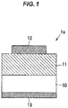
- FIG. 1 is a vertical cross-sectional view showing a Schottky barrier diode 1a in the first embodiment.
- the Schottky barrier diode 1a is a vertical Schottky barrier diode and has a first Ga203-based crystal layer 10, a second Ga 2 O 3 -based crystal layer 11 laminated on the first Ga 2 O 3 -based crystal layer 10, an anode electrode 12 connected to the second Ga 2 O 3 -based crystal layer 11, and a cathode electrode 13 connected to the first Ga 2 O 3 -based crystal layer 10.
- the first Ga 2 O 3 -based crystal layer 10 is formed of an n + type Ga 2 O 3 -based single crystal containing a Group IV element, such as Si or Sn, as a donor.
- the donor concentration in the first Ga 2 O 3 -based crystal layer 10 is, e.g., 1x10 17 to 1x10 20 cm -3 .
- the thickness of the first Ga 2 O 3 -based crystal layer 10 is, e.g., 0.5 to 1000 ⁇ m.
- the first Ga 2 O 3 -based crystal layer 10 is a Ga 2 O 3 -based substrate.
- the orientation of the principal plane of the first Ga 2 O 3 -based crystal layer 10 is, e.g., (010), (001) or (-201).
- the second Ga 2 O 3 -based crystal layer 11 is a layer formed on the first Ga 2 O 3 -based crystal layer 10 by epitaxial crystal growth and is formed of a Ga 2 O 3 -based single crystal containing an unintentionally doped donor.
- the unintentionally doped donor here includes impurities as well as defects such as oxygen vacancy.
- the concentration of the unintentionally doped donor is, e.g., not more than 1x10 18 cm -3 .
- the thickness of the second Ga 2 O 3 -based crystal layer 11 is, e.g., 0.1 to 100 ⁇ m.
- the second Ga 2 O 3 -based crystal layer 11 also contains an intentionally doped N which compensates the unintentionally doped donor.
- the N concentration in the second Ga 2 O 3 -based crystal layer 11 is preferably not more than the concentration of the unintentionally doped donor.
- N is doped during crystal growth of the second Ga203-based crystal layer 11 (in-situ doping), hence, the entire second Ga 2 O 3 -based crystal layer 11 is the N-doped region.
- a Group IV element as a donor such as Si or Sn
- the N concentration may be higher than the concentration of the unintentionally doped donor.
- the second Ga 2 O 3 -based crystal layer 11 is formed by, e.g., Molecular-beam epitaxy method (MBE method) performed using a Ga metal and an ozone gas made from an O 2 -N 2 gas mixture.
- MBE method Molecular-beam epitaxy method
- the anode electrode 12 has, e.g., a stacked structure of Pt/Ti/Au and is in Schottky contact with the second Ga 2 O 3 -based crystal layer 11.
- the cathode electrode 13 has, e.g., a stacked structure of Ti/Au and is in ohmic contact with the first Ga203-based crystal layer 10.
- an energy barrier between the anode electrode 12 and the second Ga 2 O 3 -based crystal layer 11 as viewed from the second Ga 2 O 3 -based crystal layer 11 is lowered by applying forward voltage between the anode electrode 12 and the cathode electrode 13 (positive potential on the anode electrode 12 side), allowing a current flow from the anode electrode 12 to the cathode electrode 13.
- the second Ga 2 O 3 -based crystal layer 11 which is entirely formed of the N-doped region, serves as a current path.
- reverse voltage is applied between the anode electrode 12 and the cathode electrode 13 (negative potential on the anode electrode 12 side)
- the current flow is interrupted by the Schottky barrier.
- FIG. 2 is a vertical cross-sectional view showing a Schottky barrier diode 1 b in the first embodiment.
- the Schottky barrier diode 1 b is different from the Schottky barrier diode 1 a in that it has a field-plate structure.
- an insulating film 14 formed of SiO 2 , etc., is provided on an upper surface of the second Ga 2 O 3 -based crystal layer 11 along the periphery of an anode electrode 16 which is arranged so that the edge thereof rides on the insulating film 14.
- the insulating film 14 also serves as a passivation film for preventing a surface leakage current which flows along the upper surface of the second Ga 2 O 3 -based crystal layer 11.
- FIG. 3 is a vertical cross-sectional view showing a Schottky barrier diode 1c in the first embodiment.
- the Schottky barrier diode 1c is different from the Schottky barrier diode 1b in that it has a guard ring structure.
- an N-doped region 101 as a guard ring is formed in a second Ga203-based crystal layer 15 in the vicinity of the upper surface thereof.
- the N-doped region 101 is formed in a part of the second Ga 2 O 3 -based crystal layer 15.
- the second Ga 2 O 3 -based crystal layer 15 is formed of an n - type Ga 2 O 3 -based single crystal containing a Group IV element, such as Si or Sn, as a donor.
- the donor concentration in the second Ga 2 O 3 -based crystal layer 15 is, e.g., not more than 1x10 18 cm -3 .
- the thickness of the second Ga 2 O 3 -based crystal layer 15 is, e.g., 0.1 to 100 ⁇ m.
- the N-doped region 101 is formed by, e.g., selectively implanting N ions into the upper surface of the second Ga 2 O 3 -based crystal layer 15 in a region partially overlapping the anode electrode 16.
- the N concentration in the N-doped region 101 is higher than the donor concentration in the second Ga 2 O 3 -based crystal layer 15.
- the second embodiment is an embodiment of a vertical MOSFET (Metal-Oxide-Semiconductor Field Effect Transistor) as a semiconductor device having a Ga 2 O 3 -based crystal layer in which an N-doped region is formed.
- a vertical MOSFET Metal-Oxide-Semiconductor Field Effect Transistor
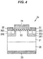
- FIG. 4 is a vertical cross-sectional view showing a vertical MOSFET 2a in the second embodiment.
- the vertical MOSFET 2a has a first Ga 2 O 3 -based crystal layer 20, a second Ga203-based crystal layer 21 laminated on the first Ga 2 O 3 -based crystal layer 20, a gate electrode 24 formed on the second Ga 2 O 3 -based crystal layer 21 via a gate insulating film 25, n + regions 202 formed in the second Ga 2 O 3 -based crystal layer 21 in the vicinity of the upper surface on both sides of the gate electrode 24, p + regions 203 formed on the outer side of the n + regions 202, an N-doped region 201 surrounding the n + regions 202 and the p + regions 203, a source electrode 22 connected to the n + regions 202 and the p + regions 203, and a drain electrode 23 formed on a surface of the first Ga 2 O 3 -based crystal layer 20 opposite to the second Ga 2 O 3 -based crystal layer 21.
- the vertical MOSFET 2a is a vertical enhancement-mode (normally-off) MOSFET.
- voltage of over a threshold is applied to the gate electrode 24, an inversion channel is formed in the N-doped region 201 under the gate electrode 24, allowing a current flow from the drain electrode 23 to the source electrode 22. That is, the N-doped region 201 includes a channel region (a region in which a channel is formed).
- the first Ga 2 O 3 -based crystal layer 20 is formed of an n + type Ga 2 O 3 -based single crystal containing a Group IV element, such as Si or Sn, as a donor.
- the donor concentration in the first Ga 2 O 3 -based crystal layer 20 is, e.g., 1x10 17 to 1x10 20 cm -3 .
- the thickness of the first Ga 2 O 3 -based crystal layer 20 is, e.g., 0.5 to 1000 ⁇ m.
- the first Ga 2 O 3 -based crystal layer 20 is a Ga 2 O 3 -based substrate.
- the orientation of the principal plane of the first Ga 2 O 3 -based crystal layer 20 is, e.g., (010), (001) or (-201).
- the second Ga 2 O 3 -based crystal layer 21 is formed of an n - type Ga 2 O 3 -based single crystal containing a Group IV element, such as Si or Sn, as a donor.
- the donor concentration in the second Ga 2 O 3 -based crystal layer 21 is, e.g., not more than 1x10 18 cm -3 .
- the thickness of the second Ga 2 O 3 -based crystal layer 21 is, e.g., 1 to 100 ⁇ m.
- the source electrode 22, the drain electrode 23 and the gate electrode 24 are formed of, e.g., Ti/Au.
- the gate insulating film 25 is formed of an insulating material such as SiO 2 .
- the n + region 202 is a region with a high n-type dopant concentration formed in the second Ga 2 O 3 -based crystal layer 21 by ion implantation, etc.
- the p + region 203 is a region with a high p-type dopant concentration formed by burying of a p-type material or ion implantation, etc., into the second Ga 2 O 3 -based crystal layer 21.
- the N-doped region 201 is a region which is formed by ion implantation, etc., and surrounds the n + regions 202 and the p + regions 203. In other words, the N-doped region 201 is formed in a part of the second Ga 2 O 3 -based crystal layer 21.
- the N concentration in the N-doped region 201 is higher than the donor concentration in the second Ga 2 O 3 -based crystal layer 21 (the region except the n + regions 202 and the p + regions 203 ).
- FIG. 5 is a vertical cross-sectional view showing a vertical MOSFET 2b in the second embodiment.
- the vertical MOSFET 2b is different from the vertical MOSFET 2a in that it is a vertical trench MOSFET with the gate electrode embedded in the second Ga 2 O 3 -based crystal layer.
- a gate electrode 26 is covered with a gate insulating film 27 and is embedded in the second Ga 2 O 3 -based crystal layer 21, and the N-doped region 201, the n + regions 202 and the p + regions 203 are located on both sides of the gate electrode 26.
- the vertical MOSFET 2b is a vertical enhancement-mode MOSFET.
- voltage of over a threshold is applied to the gate electrode 26, an inversion channel is formed in the N-doped region 201 on the lateral side of the gate electrode 26, allowing a current flow from the drain electrode 23 to the source electrode 22. That is, the N-doped region 201 includes a channel region.
- FIG. 6 is a vertical cross-sectional view showing a vertical MOSFET 2c in the second embodiment.
- the vertical MOSFET 2c is different from the vertical MOSFET 2a in that it is a vertical depletion-mode (normally-on) MOSFET in which a current blocking layer is formed.
- n + regions 205 are formed in the second Ga 2 O 3 -based crystal layer 21 in the vicinity of the upper surface on both sides of the gate electrode 24, and an N-doped region 204 as a current blocking region having an opening region is formed in a portion of the second Ga 2 O 3 -based crystal layer 21 below the n + regions 205.
- the n + region 205 is a region with a high n-type dopant concentration formed in the second Ga 2 O 3 -based crystal layer 21 by ion implantation, etc.
- the N-doped region 204 is formed in a portion below the n + regions 205 by ion implantation, etc.
- a region 204a located below the gate electrode 24 and surrounded by the N-doped region 204 is an opening region of the current blocking region and serves as a current path. That is, the N-doped region 204 is formed in a part of the second Ga 2 O 3 -based crystal layer 21.
- the N concentration in the N-doped region 204 is higher than the donor concentration in the second Ga 2 O 3 -based crystal layer 21 (the region except the n + regions 205 ).
- the vertical MOSFET 2c is a vertical depletion-mode MOSFET, as described above.
- the current can flow from the drain electrode 23 to the source electrode 22 in a state that no voltage or voltage of over a threshold is applied to the gate electrode 24, but when voltage of less than the threshold is applied to the gate electrode 24, the channel is partially closed, allowing the current to be turned off.
- the third embodiment is an embodiment of a lateral MOSFET as a semiconductor device having a Ga 2 O 3 -based crystal layer in which an N-doped region is formed.
- FIG. 7 is a vertical cross-sectional view showing a lateral MOSFET 3a in the third embodiment.
- the lateral MOSFET 3a has a first Ga 2 O 3 -based crystal layer 30, a second Ga 2 O 3 -based crystal layer 31 laminated on the first Ga 2 O 3 -based crystal layer 30, a source electrode 32 and a drain electrode 33 which are formed on the second Ga 2 O 3 -based crystal layer 31, a gate electrode 34 formed on the second Ga 2 O 3 -based crystal layer 31 via a gate insulating film 35 in a region between the source electrode 32 and the drain electrode 33, n + regions 302 formed in the second Ga 2 O 3 -based crystal layer 31 in the vicinity of the upper surface on both sides of the gate electrode 34 and respectively connected to the source electrode 32 and the drain electrode 33, and an N-doped region 301 formed in the second Ga 2 O 3 -based crystal layer 31 between the n + regions 302 and the first Ga 2 O 3 -based crystal layer 30 so as to be continuous in an in-plane direction.
- the lateral MOSFET 3a is a lateral depletion-mode MOSFET.
- the current can flow from the drain electrode 33 to the source electrode 32 in a state that no voltage is applied to the gate electrode 34, but when voltage of less than the threshold is applied to the gate electrode 34, a depletion layer expands and this causes the channel between the two n + regions 302 to be narrowed, resulting in interruption of the current flow.
- the first Ga 2 O 3 -based crystal layer 30 is a semi-insulating layer to which an acceptor impurity such as Fe is intentionally doped at a concentration higher than the donor concentration. Resistivity of the first Ga 2 O 3 -based crystal layer 30 is, e.g., larger than 1x10 10 ⁇ cm. The thickness of the first Ga 2 O 3 -based crystal layer 30 is, e.g., 0.5 to 1000 ⁇ m.
- the first Ga 2 O 3 -based crystal layer 30 is a Ga 2 O 3 -based substrate.
- the orientation of the principal plane of the first Ga 2 O 3 -based crystal layer 30 is, e.g., (010), (001) or (-201).
- the second Ga 2 O 3 -based crystal layer 31 is formed of an n - type Ga 2 O 3 -based single crystal containing a Group IV element, such as Si or Sn, as a donor.
- the donor concentration in the second Ga 2 O 3 -based crystal layer 31 is, e.g., 1x10 16 to 5x10 19 cm -3 .
- the thickness of the second Ga 2 O 3 -based crystal layer 31 is, e.g., 0.02 to 100 ⁇ m.
- the source electrode 32, the drain electrode 33 and the gate electrode 34 are formed of, e.g., Ti/Au.
- the gate insulating film 35 is formed of an insulating material such as Si02.
- the n + region 302 is a region with a high n-type dopant concentration formed in the second Ga 2 O 3 -based crystal layer 31 by ion implantation, etc.
- the N-doped region 301 is formed by ion implantation, etc., at a position blocking between a channel, which is formed between the two n + regions 302, and an interface formed between the second Ga 2 O 3 -based crystal layer 31 and the first Ga 2 O 3 -based crystal layer 30.
- the N-doped region 301 is formed between the channel region, which is formed in the second Ga 2 O 3 -based crystal layer 31 and is a part of the second Ga 2 O 3 -based crystal layer 31, and a bottom surface of the second Ga 2 O 3 -based crystal layer 31.
- the N-doped region 301 can prevent a leakage current which flows through the interface between the second Ga 2 O 3 -based crystal layer 31 and the first Ga 2 O 3 -based crystal layer 30.
- the N concentration in the N-doped region 301 is higher than the donor concentration in the second Ga 2 O 3 -based crystal layer 31 (the region except the n + regions 302 ).
- FIG. 8 is a vertical cross-sectional view showing a lateral MOSFET 3b in the third embodiment.
- the lateral MOSFET 3b is different from the lateral MOSFET 3a in that the N-doped region is formed in the entire second Ga 2 O 3 -based crystal layer.
- a second Ga 2 O 3 -based crystal layer 36 of the lateral MOSFET 3b is a layer formed on the first Ga 2 O 3 -based crystal layer 30 by epitaxial crystal growth and is formed of a Ga 2 O 3 -based single crystal containing an unintentionally doped donor.
- the concentration of the unintentionally doped donor is, e.g., not more than 1x10 18 cm -3 .
- the thickness of the second Ga 2 O 3 -based crystal layer 36 is, e.g., 0.02 to 100 ⁇ m.
- the second Ga 2 O 3 -based crystal layer 36 also contains an intentionally doped N which compensates the unintentionally doped donor.
- the N concentration in the second Ga 2 O 3 -based crystal layer 36 is preferably not more than the concentration of the unintentionally doped donor.
- N is doped during crystal growth of the second Ga 2 O 3 -based crystal layer 36, hence, the entire second Ga 2 O 3 -based crystal layer 36 is the N-doped region.
- N may be doped to the second Ga 2 O 3 -based crystal layer 36 by ion implantation.
- a Group IV element as a donor such as Si or Sn
- the N concentration may be higher than the concentration of the unintentionally doped donor.
- the lateral MOSFET 3b is a lateral depletion-mode MOSFET.
- the current can flow from the drain electrode 33 to the source electrode 32 in a state that no voltage is applied to the gate electrode 34, but when voltage of not more than the threshold is applied to the gate electrode 34, a depletion layer expands and this causes the channel between the two n + regions 302 to be narrowed, resulting in interruption of the current flow. That is, the N-doped region formed in the entire second Ga 2 O 3 -based crystal layer 36 includes a channel region.
- FIG. 9 is a vertical cross-sectional view showing a lateral MOSFET 3c in the third embodiment.
- the lateral MOSFET 3c is different from the lateral MOSFET 3b in that it is an enhancement-mode device.
- a second Ga 2 O 3 -based crystal layer 37 of the lateral MOSFET 3c is a layer formed on the first Ga 2 O 3 -based crystal layer 30 by epitaxial crystal growth and is formed of a Ga 2 O 3 -based single crystal containing an unintentionally doped donor.
- the concentration of the unintentionally doped donor is, e.g., not more than 1x10 18 cm -3 .
- the thickness of the second Ga 2 O 3 -based crystal layer 37 is, e.g., 0.02 to 100 ⁇ m.
- the second Ga 2 O 3 -based crystal layer 37 also contains an intentionally doped N which compensates the unintentionally doped donor.
- the N concentration in the second Ga 2 O 3 -based crystal layer 37 is preferably higher than the concentration of the unintentionally doped donor.
- N is doped during crystal growth of the second Ga 2 O 3 -based crystal layer 37, hence, the entire second Ga 2 O 3 -based crystal layer 37 is the N-doped region.
- N may be doped to the second Ga 2 O 3 -based crystal layer 37 by ion implantation.
- a gate electrode 38 of the lateral MOSFET 3c overlaps with, or is located very close to, end portions of the n + regions 302 so that a continuous channel region is formed between the source electrode 32 and the drain electrode 33.
- the lateral MOSFET 3c is a lateral enhancement-mode MOSFET.
- a channel is formed between the two n + regions 302 in the vicinity of the upper surface of the second Ga 2 O 3 -based crystal layer 37, allowing a current flow from the drain electrode 33 to the source electrode 32. That is, the N-doped region formed in the entire second Ga 2 O 3 -based crystal layer 37 includes a channel region.
- FIG. 10 is a vertical cross-sectional view showing a lateral MOSFET 3d in the third embodiment.
- the lateral MOSFET 3d is different from the lateral MOSFET 3c in that the N-doped region is formed only in a portion of the second Ga 2 O 3 -based crystal layer on the upper side.
- An N-doped region 303 of the lateral MOSFET 3d is formed in the second Ga 2 O 3 -based crystal layer 31 by ion implantation, etc., in an upper region including the n + regions 302. That is, the N-doped region 303 is formed in a part of the second Ga 2 O 3 -based crystal layer 31.
- the N concentration in the N-doped region 303 is higher than the donor concentration in the second Ga 2 O 3 -based crystal layer 31 (the region except the n + regions 302 ).
- the lateral MOSFET 3d is a lateral enhancement-mode MOSFET, in the same manner as the lateral MOSFET 3c.
- a channel is formed between the two n + regions 302 in the vicinity of the upper surface of the second Ga 2 O 3 -based crystal layer 31 (the N-doped region 303 ), allowing a current flow from the drain electrode 33 to the source electrode 32. That is, the N-doped region 303 includes a channel region.
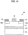
- the fourth embodiment is an embodiment of a lateral MESFET (Metal-Semiconductor Field Effect Transistor) as a semiconductor device having a Ga 2 O 3 -based crystal layer in which an N-doped region is formed.
- a lateral MESFET Metal-Semiconductor Field Effect Transistor
- FIG. 11 is a vertical cross-sectional view showing a MESFET 4a in the fourth embodiment.
- the MESFET 4a has a first Ga 2 O 3 -based crystal layer 40, a second Ga 2 O 3 -based crystal layer 41 laminated on the first Ga 2 O 3 -based crystal layer 40, a source electrode 42 and a drain electrode 43 which are formed on the second Ga 2 O 3 -based crystal layer 41, a gate electrode 44 formed on the second Ga 2 O 3 -based crystal layer 41 in a region between the source electrode 42 and the drain electrode 43, ⁇ + regions 402 formed in the second Ga 2 O 3 -based crystal layer 41 in the vicinity of the upper surface on both sides of the gate electrode 44 and respectively connected to the source electrode 42 and the drain electrode 43, and an N-doped region 401 formed in the second Ga 2 O 3 -based crystal layer 41 between the n + regions 402 and the first Ga 2 O 3 -based crystal layer 40 so as to be continuous in an in-plane direction.
- the gate electrode 44 is in Schottky contact with the upper surface of the second Ga203-based crystal layer 41 and a depletion layer is formed in the second Ga 2 O 3 -based crystal layer 41 under the gate electrode 44.
- the MESFET 4a functions as either a depletion-mode transistor or an enhancement-mode transistor depending on the thickness of the depletion region.
- the first Ga 2 O 3 -based crystal layer 40 is a semi-insulating layer to which an acceptor impurity such as Fe is intentionally doped at a concentration higher than the donor concentration. Resistivity of the first Ga 2 O 3 -based crystal layer 40 is, e.g., not less than 1x10 10 ⁇ cm. The thickness of the first Ga 2 O 3 -based crystal layer 40 is, e.g., 0.5 to 1000 ⁇ m.
- the first Ga 2 O 3 -based crystal layer 40 is a Ga 2 O 3 -based substrate.
- the orientation of the principal plane of the first Ga 2 O 3 -based crystal layer 40 is, e.g., (010), (001) or (-201).
- the second Ga 2 O 3 -based crystal layer 41 is formed of an n - type Ga 2 O 3 -based single crystal containing a Group IV element, such as Si or Sn, as a donor.
- the donor concentration in the second Ga 2 O 3 -based crystal layer 41 is, e.g., 1x10 16 to 5x10 19 cm -3 .
- the thickness of the second Ga 2 O 3 -based crystal layer 41 is, e.g., 0.02 to 100 ⁇ m.
- the source electrode 42 and the drain electrode 43 are formed of, e.g., Ti/Au.
- the gate electrode 44 is formed of, e.g., Pt/Ti/Au.
- the n + region 402 is a region with a high n-type dopant concentration formed in the second Ga 2 O 3 -based crystal layer 41 by ion implantation, etc.
- the N-doped region 401 is formed by ion implantation, etc., at a position blocking between a channel, which is formed between the two n + regions 402, and an interface formed between the second Ga 2 O 3 -based crystal layer 41 and the first Ga 2 O 3 -based crystal layer 40.
- the N-doped region 401 is formed between the channel region, which is formed in the second Ga 2 O 3 -based crystal layer 41 and is a part of the second Ga 2 O 3 -based crystal layer 41, and a bottom surface of the second Ga 2 O 3 -based crystal layer 41.
- the N-doped region 401 can prevent a leakage current which flows through the interface between the second Ga 2 O 3 -based crystal layer 41 and the first Ga 2 O 3 -based crystal layer 40.
- the N concentration in the N-doped region 401 is higher than the donor concentration in the second Ga 2 O 3 -based crystal layer 41 (the region except the n + regions 402 ).
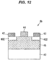
- FIG. 12 is a vertical cross-sectional view showing a MESFET 4b in the fourth embodiment.
- the MESFET 4b is different from the MESFET 4a in that the N-doped region is formed in the entire second Ga 2 O 3 -based crystal layer.
- a second Ga 2 O 3 -based crystal layer 45 of the MESFET 4b is a layer formed on the first Ga 2 O 3 -based crystal layer 40 by epitaxial crystal growth and is formed of a Ga 2 O 3 -based single crystal containing an unintentionally doped donor.
- the concentration of the unintentionally doped donor is, e.g., not more than 1x10 18 cm -3 .
- the thickness of the second Ga 2 O 3 -based crystal layer 45 is, e.g., 0.02 to 100 ⁇ m.
- the second Ga 2 O 3 -based crystal layer 45 also contains an intentionally doped N which compensates the unintentionally doped donor.
- the N concentration in the second Ga 2 O 3 -based crystal layer 45 is preferably not more than the concentration of the unintentionally doped donor.
- N is doped during crystal growth of the second Ga 2 O 3 -based crystal layer 45, hence, the entire second Ga 2 O 3 -based crystal layer 45 is the N-doped region.
- N may be doped to the second Ga 2 O 3 -based crystal layer 45 by ion implantation.
- a Group IV element as a donor such as Si or Sn
- the N concentration may be higher than the concentration of the unintentionally doped donor.
- the gate electrode 44 is in Schottky contact with the upper surface of the second Ga 2 O 3 -based crystal layer 45 and a depletion layer is formed in the second Ga 2 O 3 -based crystal layer 45 under the gate electrode 44.
- the MESFET 4b functions as either a depletion-mode transistor or an enhancement-mode transistor depending on the thickness of the depletion region.
- the first to fourth embodiments it is possible to increase resistance of Ga 2 O 3 -based crystal or to form a p-type region by using N which has not been known as an acceptor in the Ga203-based crystal. It is also possible to provide a semiconductor device having a Ga 2 O 3 -based crystal layer doped with such N.
- FIG. 13 is a vertical cross-sectional view showing a sample device 5 used in experiments in Example 1.
- the sample device 5 has a Ga 2 O 3 single crystal substrate 50 containing an unintentionally doped donor, an n + type Ga 2 O 3 single crystal layer 51 laminated on the Ga 2 O 3 single crystal substrate 50, an N-doped region 501 formed in the Ga 2 O 3 single crystal substrate 50, an n + region 502 formed in the Ga 2 O 3 single crystal substrate 50 in the vicinity of the upper surface (a surface opposite to the Ga 2 O 3 single crystal layer 51 ), an electrode 52 having a Ti/Au laminated structure and ohmic-connected to the n + region 502 of the Ga 2 O 3 single crystal substrate 50, and an electrode 53 having a Ti/Au laminated structure and ohmic-connected to the Ga 2 O 3 single crystal layer 51.
- the concentration of the unintentionally doped donor in the Ga 2 O 3 single crystal substrate 50 is about 3x10 17 cm -3 .
- the orientation of the principal plane of the Ga 2 O 3 single crystal substrate 50 is (001).
- the N-doped region 501 was formed by ion implantation of N into a layer-shaped region of the Ga 2 O 3 single crystal substrate 50 located at a depth of 600 to 700 nm from the upper surface under the implantation conditions of 4x10 13 cm -2 at 480 keV. In addition, after the ion implantation, annealing was performed in an N 2 atmosphere at 800 to 1200°C for 30 minutes to activate the doped N and to recover damage of the Ga 2 O 3 single crystal substrate 50 caused by the ion implantation. The maximum concentration of N in the N-doped region 501 was 1.5x10 18 cm -3 .
- n + region 502 was formed by ion implantation of Si into the Ga 2 O 3 single crystal substrate 50 in the vicinity of the upper surface. After the ion implantation, annealing was performed in an N2 atmosphere at 800°C for 30 minutes to activate the doped Si.
- FIG. 14 is a graph showing measured leakage characteristics of the sample device 5.
- FIG. 14 shows that leakage current decreases with an increase in an annealing temperature from 800°C to 1200°C. With an annealing temperature of 1200°C, the minimum value of leakage current at a voltage of 200V was 1 to 10 ⁇ A/cm 2 . This confirmed that N in the N-doped region 501 is acting as an acceptor.
- the Schottky barrier diode 1a in the first embodiment was made, and a relation between the N concentration in the second Ga 2 O 3 -based crystal layer 11 entirely formed of the N-doped region and electrical conduction properties of the Schottky barrier diode 1a.
- Example 2 an Sn-doped n + type Ga 2 O 3 single crystal substrate having a (001) plane as a principal plane was used as the first Ga 2 O 3 -based crystal layer 10. Si with a concentration of 5x10 19 cm -3 was ion-implanted into the back surface of the first Ga 2 O 3 -based crystal layer 10 to form a 150 nm deep box profile for an ohmic contact with the cathode electrode 13.
- a 2.6 ⁇ m-thick N-doped Ga 2 O 3 single crystal was homoepitaxially grown on the first Ga 2 O 3 -based crystal layer 10 by MBE using a Ga metal and an ozone gas made from an O 2 -N 2 gas mixture, thereby forming the second Ga203-based crystal layer 11.
- anode electrode 12 a 200 ⁇ m-diameter circular electrode having a Pt/Ti/Au stacked structure was formed as the anode electrode 12.
- FIGS. 15A, 15B and 15C show SIMS profiles of N in the second Ga 2 O 3 -based crystal layer 11 when an N 2 gas concentration in an O 2 -N 2 gas mixture used for growth of the second Ga 2 O 3 -based crystal layer 11 is respectively 0 vol%, 0.04 vol% and 0.4 vol%.
- a profile shown in a region shallower than the depth indicated by a dotted line is from the second Ga 2 O 3 -based crystal layer 11
- a profile shown in a region deeper than the depth indicated by the dotted line is from the first Ga 2 O 3 -based crystal layer 10.
- the N concentration in the second Ga 2 O 3 -based crystal layer 11 when the N 2 gas concentration in the O 2 -N 2 gas mixture is 0 vol%, 0.04 vol% and 0.4 vol%, was respectively 2.5x10 16 cm -3 , 3.4x10 16 cm -3 and 1.5x10 17 cm -3 .
- FIGS. 16A, 16B and 16C are graphs showing electrical conduction properties of the Schottky barrier diode 1a when the N2 gas concentration in the O 2 -N 2 gas mixture used for growth of the second Ga 2 O 3 -based crystal layer 11 is respectively 0 vol%, 0.04 vol% and 0.4 vol%.
- All of the Schottky barrier diodes 1a in FIGS. 16A, 16B and 16C exhibit n-type rectification properties in that a large amount of current flows only when the anode voltage is positive.
- FIG. 17 is a graph showing a relation between the N2 gas concentration in the O 2 -N 2 gas mixture used for growth of the second Ga 2 O 3 -based crystal layer 11 and forward current density when an anode voltage of the Schottky barrier diode 1a is 6V, which is derived from the current characteristics shown in FIGS. 16A, 16B and 16C .
- the forward current density shown in FIG. 17 when the N 2 gas concentration in the O 2 -N 2 gas mixture is 0 vol%, 0.04 vol% and 0.4 vol%, is respectively 4.88x10 -6 , 5.70x10 -7 and 8.76x10 -9 A/cm 2 .
- FIG. 17 shows that the current exponentially decreases with an increase in the N 2 gas concentration. This shows that the intentionally doped N in the second Ga 2 O 3 -based crystal layer 11 contributes to increase resistance of the second Ga 2 O 3 -based crystal layer 11.
- Ga 2 O 3 -based semiconductor device which has a Ga 2 O 3 -based crystal layer doped with a novel acceptor impurity.
Abstract
Description
- The invention relates to a Ga2O3-based semiconductor device.
- A technique of epitaxially growing an undoped (not containing intentionally doped dopant) Ga2O3-based crystal film on a Ga2O3-based substrate is conventionally known (e.g., Patent Literature 1).
- A semiconductor device, which has an underlying substrate formed of a Ga2O3-based crystal, a buffer layer epitaxially grown on the underlying substrate and formed of an undoped Ga2O3-based crystal, and a Ga2O3-based crystal layer formed on the buffer layer and containing Si doped as a dopant, is also conventionally known (see, e.g., Non-Patent Literature 1).
- Patent Literature 1:
JP 2017-041593 A - Non-Patent Literature 1: Man Hoi Wong, et al., "Anomalous Fe diffusion in Si-ion-implanted β-Ga2O3 and its suppression in Ga2O3 transistor structures through highly resistive buffer layers", Applied Physics Letters 106, 032105, 2015
- Ga2O3-based crystal film, when epitaxially grown without doping, sometimes becomes n-type due to an unintentional donor. In case that such undoped Ga2O3-based crystal film is used in a semiconductor device, a problem may occur due to the undoped Ga2O3-based crystal film which became n-type.
- For example, in case of FET (Field effect transistor) in which an undoped Ga2O3-based crystal film is used as a buffer layer, the FET fails to operate normally since a current also flows through the buffer layer (leakage current) in addition to through the channel layer.
- For this reason, it is sometimes required to add an appropriate acceptor to the undoped Ga2O3-based crystal layer so that the unintentionally doped donor is compensated and resistance is increased. In case of an impurity which acts as an acceptor in the Ga2O3-based crystal layer, it can be also used to form a p-type region in the undoped Ga2O3-based crystal layer or in the n-type undoped Ga2O3-based crystal layer.
- It is an object of the invention to provide a Ga2O3-based semiconductor device which has a Ga2O3-based crystal layer doped with a novel acceptor impurity.
- To achieve the above-mentioned object, an aspect of the invention provides a Ga2O3-based semiconductor device according to [1] to [8] below.
- [1] A Ga2O3-based semiconductor device, comprising a Ga2O3-based crystal layer comprising a donor, and an N (nitrogen)-doped region formed in at least a part of the Ga2O3-based crystal layer.
- [2] The Ga2O3-based semiconductor device according to [1], wherein the N-doped region comprises N at a higher concentration than the donor.
- [3] The Ga2O3-based semiconductor device according to [1] or [2], wherein the N-doped region is formed in a part of the Ga2O3-based crystal layer.
- [4] The Ga2O3-based semiconductor device according to [1], wherein the donor is unintentionally doped to the Ga2O3-based crystal layer, and the N-doped region comprises N at a concentration not more than the concentration of the donor.
- [5] The Ga2O3-based semiconductor device according to any one of [1], [2] and [4], comprising a vertical Schottky barrier diode in which the N-doped region is a current path or a guard ring.
- [6] The Ga2O3-based semiconductor device according to [1] or [2], comprising a vertical MOSFET in which the N-doped region comprises a channel region or is a current blocking region comprising an opening region as a current path.
- [7] The Ga2O3-based semiconductor device according to any one of [1], [2] and [4], comprising a lateral MOSFET in which the N-doped region comprises a channel region or is located between a channel region in the Ga2O3-based crystal layer and a bottom surface of the Ga2O3-based crystal layer.
- [8] The Ga2O3-based semiconductor device according to any one of [1], [2] and [4], comprising a MESFET in which the N-doped region comprises a channel region or is located between a channel region in the Ga2O3-based crystal layer and a bottom surface of the Ga2O3-based crystal layer.
- According to the invention, it is possible to provide a Ga2O3-based semiconductor device which has a Ga2O3-based crystal layer doped with a novel acceptor impurity.
-
-
FIG. 1 is a vertical cross-sectional view showing a Schottky barrier diode in the first embodiment. -
FIG. 2 is a vertical cross-sectional view showing a Schottky barrier diode in the first embodiment. -
FIG. 3 is a vertical cross-sectional view showing a Schottky barrier diode in the first embodiment. -
FIG. 4 is a vertical cross-sectional view showing a vertical MOSFET in the second embodiment. -
FIG. 5 is a vertical cross-sectional view showing a vertical MOSFET in the second embodiment. -
FIG. 6 is a vertical cross-sectional view showing a vertical MOSFET in the second embodiment. -
FIG. 7 is a vertical cross-sectional view showing a lateral MOSFET in the third embodiment. -
FIG. 8 is a vertical cross-sectional view showing a lateral MOSFET in the third embodiment. -
FIG. 9 is a vertical cross-sectional view showing a lateral MOSFET in the third embodiment. -
FIG. 10 is a vertical cross-sectional view showing a lateral MOSFET in the third embodiment. -
FIG. 11 is a vertical cross-sectional view showing a MESFET in the fourth embodiment. -
FIG. 12 is a vertical cross-sectional view showing a MESFET in the fourth embodiment. -
FIG. 13 is a vertical cross-sectional view showing a sample device used in experiments in Example 1. -
FIG. 14 is a graph showing measured leakage characteristics of the sample device. -
FIG. 15A is a SIMS depth profile of N density in a second Ga203-based crystal layer when a N2 gas concentration in an O2-N2 gas mixture used for growth of the second Ga2O3-based crystal layer is 0 vol%. -
FIG. 15B is a SIMS depth profile of N density in the second Ga2O3-based crystal layer when the N2 gas concentration in the O2-N2 gas mixture used for growth of the second Ga2O3-based crystal layer is 0.04 vol%. -
FIG. 15C is a SIMS depth profile of N density in the second Ga2O3-based crystal layer when the N2 gas concentration in the O2-N2 gas mixture used for growth of the second Ga2O3-based crystal layer is 0.4 vol%. -
FIG. 16A is a graph showing electrical conduction properties of the Schottky barrier diode when the N2 gas concentration in the O2-N2 gas mixture used for growth of the second Ga2O3-based crystal layer is 0 vol%. -
FIG. 16B is a graph showing electrical conduction properties of the Schottky barrier diode when the N2 gas concentration in the O2-N2 gas mixture used for growth of the second Ga2O3-based crystal layer is 0.04 vol%. -
FIG. 16C is a graph showing electrical conduction properties of the Schottky barrier diode when the N2 gas concentration in the O2-N2 gas mixture used for growth of the second Ga2O3-based crystal layer is 0.4 vol%. -
FIG. 17 is a graph showing a relation between the N2 gas concentration in the O2-N2 gas mixture used for growth of the second Ga2O3-based crystal layer and forward current density when an anode voltage of the Schottky barrier diode is 6V. - The first embodiment is an embodiment of a Schottky barrier diode as a semiconductor device having a Ga203-based crystal layer in which an N-doped region is formed.
- It has not been known that N (nitrogen) can be incorporated into Ga2O3-based crystal at a concentration high enough to affect the characteristics, and obviously, it has not been known that N acts as an acceptor in the Ga2O3-based crystal.
- Ga2O3-based single crystal here means a Ga2O3 single crystal or is a Ga2O3 single crystal doped with an element such as Al or In, and may be, e.g., a (GaxAlyIn(1-x-y))2O3 (0<x≤1, 0≤y<1, 0<x+y≤1) single crystal which is a Ga2O3 single crystal doped with Al and In. The band gap is widened by adding Al and is narrowed by adding In.
-
FIG. 1 is a vertical cross-sectional view showing aSchottky barrier diode 1a in the first embodiment. - The Schottky
barrier diode 1a is a vertical Schottky barrier diode and has a first Ga203-basedcrystal layer 10, a second Ga2O3-basedcrystal layer 11 laminated on the first Ga2O3-basedcrystal layer 10, ananode electrode 12 connected to the second Ga2O3-basedcrystal layer 11, and acathode electrode 13 connected to the first Ga2O3-basedcrystal layer 10. - The first Ga2O3-based
crystal layer 10 is formed of an n+ type Ga2O3-based single crystal containing a Group IV element, such as Si or Sn, as a donor. The donor concentration in the first Ga2O3-basedcrystal layer 10 is, e.g., 1x10¹⁷ to 1x1020 cm-3. The thickness of the first Ga2O3-basedcrystal layer 10 is, e.g., 0.5 to 1000 µm. - In a typical configuration of the
Schottky barrier diode 1a, the first Ga2O3-basedcrystal layer 10 is a Ga2O3-based substrate. The orientation of the principal plane of the first Ga2O3-basedcrystal layer 10 is, e.g., (010), (001) or (-201). - The second Ga2O3-based
crystal layer 11 is a layer formed on the first Ga2O3-basedcrystal layer 10 by epitaxial crystal growth and is formed of a Ga2O3-based single crystal containing an unintentionally doped donor. The unintentionally doped donor here includes impurities as well as defects such as oxygen vacancy. The concentration of the unintentionally doped donor is, e.g., not more than 1x1018 cm-3. The thickness of the second Ga2O3-basedcrystal layer 11 is, e.g., 0.1 to 100 µm. - The second Ga2O3-based
crystal layer 11 also contains an intentionally doped N which compensates the unintentionally doped donor. To reduce electron concentration, the N concentration in the second Ga2O3-basedcrystal layer 11 is preferably not more than the concentration of the unintentionally doped donor. N is doped during crystal growth of the second Ga203-based crystal layer 11 (in-situ doping), hence, the entire second Ga2O3-basedcrystal layer 11 is the N-doped region. However, when, e.g., a Group IV element as a donor, such as Si or Sn, is intentionally doped simultaneously with addition of N, the N concentration may be higher than the concentration of the unintentionally doped donor. - The second Ga2O3-based
crystal layer 11 is formed by, e.g., Molecular-beam epitaxy method (MBE method) performed using a Ga metal and an ozone gas made from an O2-N2 gas mixture. - The
anode electrode 12 has, e.g., a stacked structure of Pt/Ti/Au and is in Schottky contact with the second Ga2O3-basedcrystal layer 11. - The
cathode electrode 13 has, e.g., a stacked structure of Ti/Au and is in ohmic contact with the first Ga203-basedcrystal layer 10. - In the
Schottky barrier diode 1a, an energy barrier between theanode electrode 12 and the second Ga2O3-basedcrystal layer 11 as viewed from the second Ga2O3-basedcrystal layer 11 is lowered by applying forward voltage between theanode electrode 12 and the cathode electrode 13 (positive potential on theanode electrode 12 side), allowing a current flow from theanode electrode 12 to thecathode electrode 13. Thus, the second Ga2O3-basedcrystal layer 11, which is entirely formed of the N-doped region, serves as a current path. On the other hand, when reverse voltage is applied between theanode electrode 12 and the cathode electrode 13 (negative potential on theanode electrode 12 side), the current flow is interrupted by the Schottky barrier. -
FIG. 2 is a vertical cross-sectional view showing aSchottky barrier diode 1b in the first embodiment. TheSchottky barrier diode 1b is different from theSchottky barrier diode 1a in that it has a field-plate structure. - In the
Schottky barrier diode 1b, an insulatingfilm 14 formed of SiO2, etc., is provided on an upper surface of the second Ga2O3-basedcrystal layer 11 along the periphery of ananode electrode 16 which is arranged so that the edge thereof rides on the insulatingfilm 14. - By providing such field-plate structure, it is possible to prevent the electric field from concentrating at the edge portion of the
anode electrode 16. The insulatingfilm 14 also serves as a passivation film for preventing a surface leakage current which flows along the upper surface of the second Ga2O3-basedcrystal layer 11. -
FIG. 3 is a vertical cross-sectional view showing aSchottky barrier diode 1c in the first embodiment. - The
Schottky barrier diode 1c is different from theSchottky barrier diode 1b in that it has a guard ring structure. In theSchottky barrier diode 1c, an N-dopedregion 101 as a guard ring is formed in a second Ga203-basedcrystal layer 15 in the vicinity of the upper surface thereof. In other words, the N-dopedregion 101 is formed in a part of the second Ga2O3-basedcrystal layer 15. - The second Ga2O3-based
crystal layer 15 is formed of an n- type Ga2O3-based single crystal containing a Group IV element, such as Si or Sn, as a donor. The donor concentration in the second Ga2O3-basedcrystal layer 15 is, e.g., not more than 1x1018 cm-3. The thickness of the second Ga2O3-basedcrystal layer 15 is, e.g., 0.1 to 100 µm. - The N-doped
region 101 is formed by, e.g., selectively implanting N ions into the upper surface of the second Ga2O3-basedcrystal layer 15 in a region partially overlapping theanode electrode 16. The N concentration in the N-dopedregion 101 is higher than the donor concentration in the second Ga2O3-basedcrystal layer 15. By providing such a guard ring structure, it is possible to reduce concentration of the electric field at the edge portion of theanode electrode 16. - The second embodiment is an embodiment of a vertical MOSFET (Metal-Oxide-Semiconductor Field Effect Transistor) as a semiconductor device having a Ga2O3-based crystal layer in which an N-doped region is formed.
-
FIG. 4 is a vertical cross-sectional view showing avertical MOSFET 2a in the second embodiment. - The
vertical MOSFET 2a has a first Ga2O3-basedcrystal layer 20, a second Ga203-basedcrystal layer 21 laminated on the first Ga2O3-basedcrystal layer 20, agate electrode 24 formed on the second Ga2O3-basedcrystal layer 21 via agate insulating film 25, n+ regions 202 formed in the second Ga2O3-basedcrystal layer 21 in the vicinity of the upper surface on both sides of thegate electrode 24, p+ regions 203 formed on the outer side of the n+ regions 202, an N-dopedregion 201 surrounding the n+ regions 202 and the p+ regions 203, asource electrode 22 connected to the n+ regions 202 and the p+ regions 203, and adrain electrode 23 formed on a surface of the first Ga2O3-basedcrystal layer 20 opposite to the second Ga2O3-basedcrystal layer 21. - The
vertical MOSFET 2a is a vertical enhancement-mode (normally-off) MOSFET. When voltage of over a threshold is applied to thegate electrode 24, an inversion channel is formed in the N-dopedregion 201 under thegate electrode 24, allowing a current flow from thedrain electrode 23 to thesource electrode 22. That is, the N-dopedregion 201 includes a channel region (a region in which a channel is formed). - The first Ga2O3-based
crystal layer 20 is formed of an n+ type Ga2O3-based single crystal containing a Group IV element, such as Si or Sn, as a donor. The donor concentration in the first Ga2O3-basedcrystal layer 20 is, e.g., 1x10¹⁷ to 1x1020 cm-3. The thickness of the first Ga2O3-basedcrystal layer 20 is, e.g., 0.5 to 1000 µm. - In a typical configuration of the
vertical MOSFET 2a, the first Ga2O3-basedcrystal layer 20 is a Ga2O3-based substrate. The orientation of the principal plane of the first Ga2O3-basedcrystal layer 20 is, e.g., (010), (001) or (-201). - The second Ga2O3-based
crystal layer 21 is formed of an n- type Ga2O3-based single crystal containing a Group IV element, such as Si or Sn, as a donor. The donor concentration in the second Ga2O3-basedcrystal layer 21 is, e.g., not more than 1x1018 cm-3. The thickness of the second Ga2O3-basedcrystal layer 21 is, e.g., 1 to 100 µm. - The
source electrode 22, thedrain electrode 23 and thegate electrode 24 are formed of, e.g., Ti/Au. Thegate insulating film 25 is formed of an insulating material such as SiO2. - The n+ region 202 is a region with a high n-type dopant concentration formed in the second Ga2O3-based
crystal layer 21 by ion implantation, etc. The p+ region 203 is a region with a high p-type dopant concentration formed by burying of a p-type material or ion implantation, etc., into the second Ga2O3-basedcrystal layer 21. - The N-doped
region 201 is a region which is formed by ion implantation, etc., and surrounds the n+ regions 202 and the p+ regions 203. In other words, the N-dopedregion 201 is formed in a part of the second Ga2O3-basedcrystal layer 21. The N concentration in the N-dopedregion 201 is higher than the donor concentration in the second Ga2O3-based crystal layer 21 (the region except the n+ regions 202 and the p+ regions 203). -
FIG. 5 is a vertical cross-sectional view showing avertical MOSFET 2b in the second embodiment. Thevertical MOSFET 2b is different from thevertical MOSFET 2a in that it is a vertical trench MOSFET with the gate electrode embedded in the second Ga2O3-based crystal layer. - In the
vertical MOSFET 2b, agate electrode 26 is covered with agate insulating film 27 and is embedded in the second Ga2O3-basedcrystal layer 21, and the N-dopedregion 201, the n+ regions 202 and the p+ regions 203 are located on both sides of thegate electrode 26. - The
vertical MOSFET 2b is a vertical enhancement-mode MOSFET. When voltage of over a threshold is applied to thegate electrode 26, an inversion channel is formed in the N-dopedregion 201 on the lateral side of thegate electrode 26, allowing a current flow from thedrain electrode 23 to thesource electrode 22. That is, the N-dopedregion 201 includes a channel region. -
FIG. 6 is a vertical cross-sectional view showing a vertical MOSFET 2c in the second embodiment. The vertical MOSFET 2c is different from thevertical MOSFET 2a in that it is a vertical depletion-mode (normally-on) MOSFET in which a current blocking layer is formed. - In the vertical MOSFET 2c, n+ regions 205 are formed in the second Ga2O3-based
crystal layer 21 in the vicinity of the upper surface on both sides of thegate electrode 24, and an N-dopedregion 204 as a current blocking region having an opening region is formed in a portion of the second Ga2O3-basedcrystal layer 21 below the n+ regions 205. - The n+ region 205 is a region with a high n-type dopant concentration formed in the second Ga2O3-based
crystal layer 21 by ion implantation, etc. - The N-doped
region 204 is formed in a portion below the n+ regions 205 by ion implantation, etc. Aregion 204a located below thegate electrode 24 and surrounded by the N-dopedregion 204 is an opening region of the current blocking region and serves as a current path. That is, the N-dopedregion 204 is formed in a part of the second Ga2O3-basedcrystal layer 21. The N concentration in the N-dopedregion 204 is higher than the donor concentration in the second Ga2O3-based crystal layer 21 (the region except the n+ regions 205). - The vertical MOSFET 2c is a vertical depletion-mode MOSFET, as described above. The current can flow from the
drain electrode 23 to thesource electrode 22 in a state that no voltage or voltage of over a threshold is applied to thegate electrode 24, but when voltage of less than the threshold is applied to thegate electrode 24, the channel is partially closed, allowing the current to be turned off. - The third embodiment is an embodiment of a lateral MOSFET as a semiconductor device having a Ga2O3-based crystal layer in which an N-doped region is formed.
-
FIG. 7 is a vertical cross-sectional view showing alateral MOSFET 3a in the third embodiment. - The
lateral MOSFET 3a has a first Ga2O3-basedcrystal layer 30, a second Ga2O3-basedcrystal layer 31 laminated on the first Ga2O3-basedcrystal layer 30, asource electrode 32 and adrain electrode 33 which are formed on the second Ga2O3-basedcrystal layer 31, agate electrode 34 formed on the second Ga2O3-basedcrystal layer 31 via agate insulating film 35 in a region between thesource electrode 32 and thedrain electrode 33, n+ regions 302 formed in the second Ga2O3-basedcrystal layer 31 in the vicinity of the upper surface on both sides of thegate electrode 34 and respectively connected to thesource electrode 32 and thedrain electrode 33, and an N-dopedregion 301 formed in the second Ga2O3-basedcrystal layer 31 between the n+ regions 302 and the first Ga2O3-basedcrystal layer 30 so as to be continuous in an in-plane direction. - The
lateral MOSFET 3a is a lateral depletion-mode MOSFET. The current can flow from thedrain electrode 33 to thesource electrode 32 in a state that no voltage is applied to thegate electrode 34, but when voltage of less than the threshold is applied to thegate electrode 34, a depletion layer expands and this causes the channel between the two n+ regions 302 to be narrowed, resulting in interruption of the current flow. - The first Ga2O3-based
crystal layer 30 is a semi-insulating layer to which an acceptor impurity such as Fe is intentionally doped at a concentration higher than the donor concentration. Resistivity of the first Ga2O3-basedcrystal layer 30 is, e.g., larger than 1x10¹⁰ Ωcm. The thickness of the first Ga2O3-basedcrystal layer 30 is, e.g., 0.5 to 1000 µm. - In a typical configuration of the
lateral MOSFET 3a, the first Ga2O3-basedcrystal layer 30 is a Ga2O3-based substrate. The orientation of the principal plane of the first Ga2O3-basedcrystal layer 30 is, e.g., (010), (001) or (-201). - The second Ga2O3-based
crystal layer 31 is formed of an n- type Ga2O3-based single crystal containing a Group IV element, such as Si or Sn, as a donor. The donor concentration in the second Ga2O3-basedcrystal layer 31 is, e.g., 1x10¹⁶ to 5x1019 cm-3. The thickness of the second Ga2O3-basedcrystal layer 31 is, e.g., 0.02 to 100 µm. - The
source electrode 32, thedrain electrode 33 and thegate electrode 34 are formed of, e.g., Ti/Au. Thegate insulating film 35 is formed of an insulating material such as Si02. - The n+ region 302 is a region with a high n-type dopant concentration formed in the second Ga2O3-based
crystal layer 31 by ion implantation, etc. - The N-doped
region 301 is formed by ion implantation, etc., at a position blocking between a channel, which is formed between the two n+ regions 302, and an interface formed between the second Ga2O3-basedcrystal layer 31 and the first Ga2O3-basedcrystal layer 30. In other words, the N-dopedregion 301 is formed between the channel region, which is formed in the second Ga2O3-basedcrystal layer 31 and is a part of the second Ga2O3-basedcrystal layer 31, and a bottom surface of the second Ga2O3-basedcrystal layer 31. Thus, the N-dopedregion 301 can prevent a leakage current which flows through the interface between the second Ga2O3-basedcrystal layer 31 and the first Ga2O3-basedcrystal layer 30. The N concentration in the N-dopedregion 301 is higher than the donor concentration in the second Ga2O3-based crystal layer 31 (the region except the n+ regions 302). -
FIG. 8 is a vertical cross-sectional view showing alateral MOSFET 3b in the third embodiment. Thelateral MOSFET 3b is different from thelateral MOSFET 3a in that the N-doped region is formed in the entire second Ga2O3-based crystal layer. - A second Ga2O3-based
crystal layer 36 of thelateral MOSFET 3b is a layer formed on the first Ga2O3-basedcrystal layer 30 by epitaxial crystal growth and is formed of a Ga2O3-based single crystal containing an unintentionally doped donor. The concentration of the unintentionally doped donor is, e.g., not more than 1x1018 cm-3. The thickness of the second Ga2O3-basedcrystal layer 36 is, e.g., 0.02 to 100 µm. - The second Ga2O3-based
crystal layer 36 also contains an intentionally doped N which compensates the unintentionally doped donor. To reduce electron concentration, the N concentration in the second Ga2O3-basedcrystal layer 36 is preferably not more than the concentration of the unintentionally doped donor. N is doped during crystal growth of the second Ga2O3-basedcrystal layer 36, hence, the entire second Ga2O3-basedcrystal layer 36 is the N-doped region. Alternatively, N may be doped to the second Ga2O3-basedcrystal layer 36 by ion implantation. When, e.g., a Group IV element as a donor, such as Si or Sn, is intentionally doped simultaneously with addition of N, the N concentration may be higher than the concentration of the unintentionally doped donor. - The
lateral MOSFET 3b is a lateral depletion-mode MOSFET. The current can flow from thedrain electrode 33 to thesource electrode 32 in a state that no voltage is applied to thegate electrode 34, but when voltage of not more than the threshold is applied to thegate electrode 34, a depletion layer expands and this causes the channel between the two n+ regions 302 to be narrowed, resulting in interruption of the current flow. That is, the N-doped region formed in the entire second Ga2O3-basedcrystal layer 36 includes a channel region. -
FIG. 9 is a vertical cross-sectional view showing alateral MOSFET 3c in the third embodiment. Thelateral MOSFET 3c is different from thelateral MOSFET 3b in that it is an enhancement-mode device. - A second Ga2O3-based
crystal layer 37 of thelateral MOSFET 3c is a layer formed on the first Ga2O3-basedcrystal layer 30 by epitaxial crystal growth and is formed of a Ga2O3-based single crystal containing an unintentionally doped donor. The concentration of the unintentionally doped donor is, e.g., not more than 1x1018 cm-3. The thickness of the second Ga2O3-basedcrystal layer 37 is, e.g., 0.02 to 100 µm. - The second Ga2O3-based
crystal layer 37 also contains an intentionally doped N which compensates the unintentionally doped donor. The N concentration in the second Ga2O3-basedcrystal layer 37 is preferably higher than the concentration of the unintentionally doped donor. N is doped during crystal growth of the second Ga2O3-basedcrystal layer 37, hence, the entire second Ga2O3-basedcrystal layer 37 is the N-doped region. Alternatively, N may be doped to the second Ga2O3-basedcrystal layer 37 by ion implantation. - A
gate electrode 38 of thelateral MOSFET 3c overlaps with, or is located very close to, end portions of the n+ regions 302 so that a continuous channel region is formed between thesource electrode 32 and thedrain electrode 33. - The
lateral MOSFET 3c is a lateral enhancement-mode MOSFET. When voltage of over a threshold is applied to thegate electrode 38, a channel is formed between the two n+ regions 302 in the vicinity of the upper surface of the second Ga2O3-basedcrystal layer 37, allowing a current flow from thedrain electrode 33 to thesource electrode 32. That is, the N-doped region formed in the entire second Ga2O3-basedcrystal layer 37 includes a channel region. -
FIG. 10 is a vertical cross-sectional view showing alateral MOSFET 3d in the third embodiment. Thelateral MOSFET 3d is different from thelateral MOSFET 3c in that the N-doped region is formed only in a portion of the second Ga2O3-based crystal layer on the upper side. - An N-doped
region 303 of thelateral MOSFET 3d is formed in the second Ga2O3-basedcrystal layer 31 by ion implantation, etc., in an upper region including the n+ regions 302. That is, the N-dopedregion 303 is formed in a part of the second Ga2O3-basedcrystal layer 31. The N concentration in the N-dopedregion 303 is higher than the donor concentration in the second Ga2O3-based crystal layer 31 (the region except the n+ regions 302). - The
lateral MOSFET 3d is a lateral enhancement-mode MOSFET, in the same manner as thelateral MOSFET 3c. When voltage of over a threshold is applied to thegate electrode 38, a channel is formed between the two n+ regions 302 in the vicinity of the upper surface of the second Ga2O3-based crystal layer 31 (the N-doped region 303), allowing a current flow from thedrain electrode 33 to thesource electrode 32. That is, the N-dopedregion 303 includes a channel region. - The fourth embodiment is an embodiment of a lateral MESFET (Metal-Semiconductor Field Effect Transistor) as a semiconductor device having a Ga2O3-based crystal layer in which an N-doped region is formed.
-
FIG. 11 is a vertical cross-sectional view showing aMESFET 4a in the fourth embodiment. - The
MESFET 4a has a first Ga2O3-basedcrystal layer 40, a second Ga2O3-basedcrystal layer 41 laminated on the first Ga2O3-basedcrystal layer 40, asource electrode 42 and adrain electrode 43 which are formed on the second Ga2O3-basedcrystal layer 41, agate electrode 44 formed on the second Ga2O3-basedcrystal layer 41 in a region between thesource electrode 42 and thedrain electrode 43, η+regions 402 formed in the second Ga2O3-basedcrystal layer 41 in the vicinity of the upper surface on both sides of thegate electrode 44 and respectively connected to thesource electrode 42 and thedrain electrode 43, and an N-dopedregion 401 formed in the second Ga2O3-basedcrystal layer 41 between the n+ regions 402 and the first Ga2O3-basedcrystal layer 40 so as to be continuous in an in-plane direction. - The
gate electrode 44 is in Schottky contact with the upper surface of the second Ga203-basedcrystal layer 41 and a depletion layer is formed in the second Ga2O3-basedcrystal layer 41 under thegate electrode 44. TheMESFET 4a functions as either a depletion-mode transistor or an enhancement-mode transistor depending on the thickness of the depletion region. - The first Ga2O3-based
crystal layer 40 is a semi-insulating layer to which an acceptor impurity such as Fe is intentionally doped at a concentration higher than the donor concentration. Resistivity of the first Ga2O3-basedcrystal layer 40 is, e.g., not less than 1x10¹⁰ Ωcm. The thickness of the first Ga2O3-basedcrystal layer 40 is, e.g., 0.5 to 1000 µm. - In a typical configuration of the
MESFET 4a, the first Ga2O3-basedcrystal layer 40 is a Ga2O3-based substrate. The orientation of the principal plane of the first Ga2O3-basedcrystal layer 40 is, e.g., (010), (001) or (-201). - The second Ga2O3-based
crystal layer 41 is formed of an n- type Ga2O3-based single crystal containing a Group IV element, such as Si or Sn, as a donor. The donor concentration in the second Ga2O3-basedcrystal layer 41 is, e.g., 1x10¹⁶ to 5x1019 cm-3. The thickness of the second Ga2O3-basedcrystal layer 41 is, e.g., 0.02 to 100 µm. - The
source electrode 42 and thedrain electrode 43 are formed of, e.g., Ti/Au. Thegate electrode 44 is formed of, e.g., Pt/Ti/Au. - The n+ region 402 is a region with a high n-type dopant concentration formed in the second Ga2O3-based
crystal layer 41 by ion implantation, etc. - The N-doped
region 401 is formed by ion implantation, etc., at a position blocking between a channel, which is formed between the two n+ regions 402, and an interface formed between the second Ga2O3-basedcrystal layer 41 and the first Ga2O3-basedcrystal layer 40. In other words, the N-dopedregion 401 is formed between the channel region, which is formed in the second Ga2O3-basedcrystal layer 41 and is a part of the second Ga2O3-basedcrystal layer 41, and a bottom surface of the second Ga2O3-basedcrystal layer 41. Thus, the N-dopedregion 401 can prevent a leakage current which flows through the interface between the second Ga2O3-basedcrystal layer 41 and the first Ga2O3-basedcrystal layer 40. The N concentration in the N-dopedregion 401 is higher than the donor concentration in the second Ga2O3-based crystal layer 41 (the region except the n+ regions 402). -
FIG. 12 is a vertical cross-sectional view showing aMESFET 4b in the fourth embodiment. TheMESFET 4b is different from theMESFET 4a in that the N-doped region is formed in the entire second Ga2O3-based crystal layer. - A second Ga2O3-based
crystal layer 45 of theMESFET 4b is a layer formed on the first Ga2O3-basedcrystal layer 40 by epitaxial crystal growth and is formed of a Ga2O3-based single crystal containing an unintentionally doped donor. The concentration of the unintentionally doped donor is, e.g., not more than 1x1018 cm-3. The thickness of the second Ga2O3-basedcrystal layer 45 is, e.g., 0.02 to 100 µm. - The second Ga2O3-based
crystal layer 45 also contains an intentionally doped N which compensates the unintentionally doped donor. To reduce electron concentration, the N concentration in the second Ga2O3-basedcrystal layer 45 is preferably not more than the concentration of the unintentionally doped donor. N is doped during crystal growth of the second Ga2O3-basedcrystal layer 45, hence, the entire second Ga2O3-basedcrystal layer 45 is the N-doped region. Alternatively, N may be doped to the second Ga2O3-basedcrystal layer 45 by ion implantation. When, e.g., a Group IV element as a donor, such as Si or Sn, is intentionally doped simultaneously with addition of N, the N concentration may be higher than the concentration of the unintentionally doped donor. - The
gate electrode 44 is in Schottky contact with the upper surface of the second Ga2O3-basedcrystal layer 45 and a depletion layer is formed in the second Ga2O3-basedcrystal layer 45 under thegate electrode 44. TheMESFET 4b functions as either a depletion-mode transistor or an enhancement-mode transistor depending on the thickness of the depletion region. - According to the first to fourth embodiments, it is possible to increase resistance of Ga2O3-based crystal or to form a p-type region by using N which has not been known as an acceptor in the Ga203-based crystal. It is also possible to provide a semiconductor device having a Ga2O3-based crystal layer doped with such N.
- Experiments confirmed that N doped to Ga2O3-based crystal acts as an acceptor.
-
FIG. 13 is a vertical cross-sectional view showing asample device 5 used in experiments in Example 1. Thesample device 5 has a Ga2O3single crystal substrate 50 containing an unintentionally doped donor, an n+ type Ga2O3single crystal layer 51 laminated on the Ga2O3single crystal substrate 50, an N-dopedregion 501 formed in the Ga2O3single crystal substrate 50, an n+ region 502 formed in the Ga2O3single crystal substrate 50 in the vicinity of the upper surface (a surface opposite to the Ga2O3 single crystal layer 51), anelectrode 52 having a Ti/Au laminated structure and ohmic-connected to the n+ region 502 of the Ga2O3single crystal substrate 50, and anelectrode 53 having a Ti/Au laminated structure and ohmic-connected to the Ga2O3single crystal layer 51. - The concentration of the unintentionally doped donor in the Ga2O3
single crystal substrate 50 is about 3x1017 cm-3. The orientation of the principal plane of the Ga2O3single crystal substrate 50 is (001). - The N-doped
region 501 was formed by ion implantation of N into a layer-shaped region of the Ga2O3single crystal substrate 50 located at a depth of 600 to 700 nm from the upper surface under the implantation conditions of 4x1013 cm-2 at 480 keV. In addition, after the ion implantation, annealing was performed in an N2 atmosphere at 800 to 1200°C for 30 minutes to activate the doped N and to recover damage of the Ga2O3single crystal substrate 50 caused by the ion implantation. The maximum concentration of N in the N-dopedregion 501 was 1.5x1018 cm-3. - The n+ region 502 was formed by ion implantation of Si into the Ga2O3
single crystal substrate 50 in the vicinity of the upper surface. After the ion implantation, annealing was performed in an N2 atmosphere at 800°C for 30 minutes to activate the doped Si. - Voltage was applied between the
electrode 52 and theelectrode 53 of thesample device 5 and the magnitude of vertical leakage current was measured. The result confirmed that N in the N-dopedregion 501 is acting as an acceptor. -
FIG. 14 is a graph showing measured leakage characteristics of thesample device 5.FIG. 14 shows that leakage current decreases with an increase in an annealing temperature from 800°C to 1200°C. With an annealing temperature of 1200°C, the minimum value of leakage current at a voltage of 200V was 1 to 10 µA/cm2. This confirmed that N in the N-dopedregion 501 is acting as an acceptor. - The
Schottky barrier diode 1a in the first embodiment was made, and a relation between the N concentration in the second Ga2O3-basedcrystal layer 11 entirely formed of the N-doped region and electrical conduction properties of theSchottky barrier diode 1a. - In Example 2, an Sn-doped n+ type Ga2O3 single crystal substrate having a (001) plane as a principal plane was used as the first Ga2O3-based
crystal layer 10. Si with a concentration of 5x1019 cm-3 was ion-implanted into the back surface of the first Ga2O3-basedcrystal layer 10 to form a 150 nm deep box profile for an ohmic contact with thecathode electrode 13. - Then, a 2.6 µm-thick N-doped Ga2O3 single crystal was homoepitaxially grown on the first Ga2O3-based
crystal layer 10 by MBE using a Ga metal and an ozone gas made from an O2-N2 gas mixture, thereby forming the second Ga203-basedcrystal layer 11. - Then, a 200 µm-diameter circular electrode having a Pt/Ti/Au stacked structure was formed as the
anode electrode 12. An electrode having a Ti/Au stacked structure was formed as thecathode electrode 13. - Firstly, to make sure that the second Ga2O3-based
crystal layer 11 was doped with N, secondary-ion mass spectrometry (SIMS) measurement was performed on a sample device without theanode electrode 12 and thecathode electrode 13. -
FIGS. 15A, 15B and 15C show SIMS profiles of N in the second Ga2O3-basedcrystal layer 11 when an N2 gas concentration in an O2-N2 gas mixture used for growth of the second Ga2O3-basedcrystal layer 11 is respectively 0 vol%, 0.04 vol% and 0.4 vol%. In the drawings, a profile shown in a region shallower than the depth indicated by a dotted line (a region on the left side of the dotted line) is from the second Ga2O3-basedcrystal layer 11, and a profile shown in a region deeper than the depth indicated by the dotted line (a region on the right side of the dotted line) is from the first Ga2O3-basedcrystal layer 10. - As shown in
FIGS. 15A, 15B and 15C , the N concentration in the second Ga2O3-basedcrystal layer 11, when the N2 gas concentration in the O2-N2 gas mixture is 0 vol%, 0.04 vol% and 0.4 vol%, was respectively 2.5x1016 cm-3, 3.4x1016 cm-3 and 1.5x1017 cm-3. This shows that it is possible to dope N to Ga2O3-based crystal and it is also possible to control the N concentration in the Ga2O3-based crystal by adjusting the N concentration in a source gas of ozone. - Next, electrical conduction properties of the
Schottky barrier diode 1a were measured using a sample having theanode electrode 12 and thecathode electrode 13. -
FIGS. 16A, 16B and 16C are graphs showing electrical conduction properties of theSchottky barrier diode 1a when the N2 gas concentration in the O2-N2 gas mixture used for growth of the second Ga2O3-basedcrystal layer 11 is respectively 0 vol%, 0.04 vol% and 0.4 vol%. - All of the
Schottky barrier diodes 1a inFIGS. 16A, 16B and 16C exhibit n-type rectification properties in that a large amount of current flows only when the anode voltage is positive. -
FIG. 17 is a graph showing a relation between the N2 gas concentration in the O2-N2 gas mixture used for growth of the second Ga2O3-basedcrystal layer 11 and forward current density when an anode voltage of theSchottky barrier diode 1a is 6V, which is derived from the current characteristics shown inFIGS. 16A, 16B and 16C . - The forward current density shown in
FIG. 17 , when the N2 gas concentration in the O2-N2 gas mixture is 0 vol%, 0.04 vol% and 0.4 vol%, is respectively 4.88x10⁻⁶, 5.70x10⁻⁷ and 8.76x10⁻⁹ A/cm2. -
FIG. 17 shows that the current exponentially decreases with an increase in the N2 gas concentration. This shows that the intentionally doped N in the second Ga2O3-basedcrystal layer 11 contributes to increase resistance of the second Ga2O3-basedcrystal layer 11. - Although the embodiments and Examples of the invention have been described, the invention is not intended to be limited to the embodiments and Examples, and the various kinds of modifications can be implemented without departing from the gist of the invention. In addition, the constituent elements in the embodiment and Examples can be arbitrarily combined without departing from the gist of the invention.
- In addition, the invention according to claims is not to be limited to the embodiments and Examples described above. Further, it should be noted that all combinations of the features described in the embodiments and Examples are not necessary to solve the problem of the invention.
- Provided is a Ga2O3-based semiconductor device which has a Ga2O3-based crystal layer doped with a novel acceptor impurity.
-
- 1a, 1b, 1c SCHOTTKY BARRIER DIODE
- 2a, 2b, 2c VERTICAL MOSFET
- 3a, 3b, 3c,
3d LATERAL MOSFET 3a - 4a,
4b MESFET 4b - 10, 20, 30, 40 FIRST Ga2O3-BASED CRYSTAL LAYER
- 11, 15, 21, 31, 36, 41, 45 SECOND Ga2O3-BASED CRYSTAL LAYER
- 101, 201, 204, 301, 303, 401 N-DOPED REGION
Claims (8)
- A Ga2O3-based semiconductor device, comprising:a Ga2O3-based crystal layer comprising a donor; andan N-doped region formed in at least a part of the Ga2O3-based crystal layer.
- The Ga2O3-based semiconductor device according to claim 1, wherein the N-doped region comprises N at a higher concentration than the donor.
- The Ga2O3-based semiconductor device according to claim 1 or 2, wherein the N-doped region is formed in a part of the Ga2O3-based crystal layer.
- The Ga2O3-based semiconductor device according to claim 1, wherein the donor is unintentionally doped to the Ga2O3-based crystal layer, and the N-doped region comprises N at a concentration not more than the concentration of the donor.
- The Ga2O3-based semiconductor device according to any one of claims 1, 2 and 4, comprising a vertical Schottky barrier diode in which the N-doped region is a current path or a guard ring.
- The Ga2O3-based semiconductor device according to claim 1 or 2, comprising a vertical MOSFET in which the N-doped region comprises a channel region or is a current blocking region comprising an opening region as a current path.
- The Ga2O3-based semiconductor device according to any one of claims 1, 2 and 4, comprising a lateral MOSFET in which the N-doped region comprises a channel region or is located between a channel region in the Ga2O3-based crystal layer and a bottom surface of the Ga2O3-based crystal layer.
- The Ga2O3-based semiconductor device according to any one of claims 1, 2 and 4, comprising a MESFET in which the N-doped region comprises a channel region or is located between a channel region in the Ga2O3-based crystal layer and a bottom surface of the Ga2O3-based crystal layer.
Applications Claiming Priority (2)
| Application Number | Priority Date | Filing Date | Title |
|---|---|---|---|
| JP2017088866A JP7008293B2 (en) | 2017-04-27 | 2017-04-27 | Ga2O3 series semiconductor element |
| PCT/JP2018/017007 WO2018199241A1 (en) | 2017-04-27 | 2018-04-26 | Ga2o3-based semiconductor device |
Publications (2)
| Publication Number | Publication Date |
|---|---|
| EP3629379A1 true EP3629379A1 (en) | 2020-04-01 |
| EP3629379A4 EP3629379A4 (en) | 2020-12-23 |
Family
ID=63918656
Family Applications (1)
| Application Number | Title | Priority Date | Filing Date |
|---|---|---|---|
| EP18790539.3A Pending EP3629379A4 (en) | 2017-04-27 | 2018-04-26 | Ga2o3-based semiconductor device |
Country Status (5)
| Country | Link |
|---|---|
| US (1) | US11563092B2 (en) |
| EP (1) | EP3629379A4 (en) |
| JP (1) | JP7008293B2 (en) |
| CN (1) | CN110622319A (en) |
| WO (1) | WO2018199241A1 (en) |
Families Citing this family (18)
| Publication number | Priority date | Publication date | Assignee | Title |
|---|---|---|---|---|
| KR102183959B1 (en) * | 2019-04-26 | 2020-11-27 | 홍익대학교 산학협력단 | Schottky barrier diodes with improving breakdown voltage and manufacturing method for the same |
| CN110265486B (en) | 2019-06-20 | 2023-03-24 | 中国电子科技集团公司第十三研究所 | Gallium oxide SBD terminal structure and preparation method |
| CN110350028B (en) * | 2019-07-02 | 2022-04-05 | 深圳第三代半导体研究院 | Nitrogen-doped gallium oxide thin film structure and preparation method thereof |
| JPWO2021106809A1 (en) * | 2019-11-29 | 2021-06-03 | ||
| CN111128746B (en) * | 2019-12-05 | 2022-06-07 | 中国电子科技集团公司第十三研究所 | Schottky diode and preparation method thereof |
| JP7238847B2 (en) * | 2020-04-16 | 2023-03-14 | トヨタ自動車株式会社 | Semiconductor device manufacturing method |
| JP7347335B2 (en) * | 2020-05-29 | 2023-09-20 | 豊田合成株式会社 | semiconductor equipment |
| JP7331783B2 (en) * | 2020-05-29 | 2023-08-23 | 豊田合成株式会社 | Semiconductor device manufacturing method |
| JP7327283B2 (en) * | 2020-05-29 | 2023-08-16 | 豊田合成株式会社 | semiconductor equipment |
| KR102201924B1 (en) * | 2020-08-13 | 2021-01-11 | 한국세라믹기술원 | Manufacturing method of gallium oxide thin film for power semiconductor using dopant activation technoloty |
| CN112382665A (en) * | 2020-11-03 | 2021-02-19 | 广东省科学院半导体研究所 | Gallium oxide-based MOSFET device and manufacturing method thereof |
| JPWO2022230834A1 (en) * | 2021-04-26 | 2022-11-03 | ||
| CN117441234A (en) | 2021-04-26 | 2024-01-23 | 株式会社Flosfia | Semiconductor device with a semiconductor device having a plurality of semiconductor chips |
| CN117223111A (en) | 2021-04-26 | 2023-12-12 | 株式会社Flosfia | Semiconductor device with a semiconductor device having a plurality of semiconductor chips |
| JPWO2022230830A1 (en) * | 2021-04-26 | 2022-11-03 | ||
| CN113193053B (en) * | 2021-05-20 | 2023-11-07 | 电子科技大学 | Trench schottky diode with high forward current density |
| JP2024050122A (en) * | 2022-09-29 | 2024-04-10 | 株式会社ノベルクリスタルテクノロジー | Method for growing single crystal, method for manufacturing semiconductor substrate, and semiconductor substrate |
| CN117012836A (en) * | 2023-10-07 | 2023-11-07 | 深圳市港祥辉电子有限公司 | Longitudinal gallium oxide MOSFET device and preparation method thereof |
Family Cites Families (36)
| Publication number | Priority date | Publication date | Assignee | Title |
|---|---|---|---|---|
| US6756320B2 (en) * | 2002-01-18 | 2004-06-29 | Freescale Semiconductor, Inc. | Method of forming article comprising an oxide layer on a GaAs-based semiconductor structure |
| US7982239B2 (en) * | 2007-06-13 | 2011-07-19 | Northrop Grumman Corporation | Power switching transistors |
| JP2010141037A (en) | 2008-12-10 | 2010-06-24 | Sumitomo Electric Ind Ltd | Gallium nitride based semiconductor electronic device and method of producing the same, and epitaxial substrate and method of producing the same |
| US10312361B2 (en) * | 2011-06-20 | 2019-06-04 | The Regents Of The University Of California | Trenched vertical power field-effect transistors with improved on-resistance and breakdown voltage |
| EP2721640A1 (en) * | 2011-06-20 | 2014-04-23 | The Regents Of The University Of California | Current aperture vertical electron transistors |
| US20140217470A1 (en) * | 2011-09-08 | 2014-08-07 | Tamura Corporation | Ga2O3 SEMICONDUCTOR ELEMENT |
| CN110010670A (en) | 2011-09-08 | 2019-07-12 | 株式会社田村制作所 | Ga2O3It is MISFET and Ga2O3It is MESFET |
| CN103781947B (en) * | 2011-09-08 | 2019-05-10 | 株式会社田村制作所 | Crystal laminate structure |
| US9461124B2 (en) | 2011-09-08 | 2016-10-04 | Tamura Corporation | Ga2O3 semiconductor element |
| JP2013102081A (en) * | 2011-11-09 | 2013-05-23 | Tamura Seisakusho Co Ltd | Schottky barrier diode |
| JP6112600B2 (en) * | 2012-12-10 | 2017-04-12 | ローム株式会社 | Semiconductor device and manufacturing method of semiconductor device |
| JP2014127573A (en) * | 2012-12-26 | 2014-07-07 | Rohm Co Ltd | Semiconductor device |
| JP6284140B2 (en) * | 2013-06-17 | 2018-02-28 | 株式会社タムラ製作所 | Ga2O3 semiconductor device |
| JP5984069B2 (en) * | 2013-09-30 | 2016-09-06 | 株式会社タムラ製作所 | Method for growing β-Ga2O3 single crystal film and crystal laminated structure |
| EP2874187B1 (en) * | 2013-11-15 | 2020-01-01 | Evonik Operations GmbH | Low contact resistance thin film transistor |
| WO2015171873A1 (en) * | 2014-05-07 | 2015-11-12 | Cambridge Electronics, Inc. | Transistor structure having buried island regions |
| US9590050B2 (en) * | 2014-05-08 | 2017-03-07 | Flosfia, Inc. | Crystalline multilayer structure and semiconductor device |
| WO2015200885A1 (en) * | 2014-06-27 | 2015-12-30 | Massachusetts Institute Of Technology | Structures for nitride vertical transistors |
| KR102125822B1 (en) * | 2014-07-22 | 2020-06-23 | 가부시키가이샤 플로스피아 | Crystalline semiconductor film, plate-like body and semiconductor device |
| JP2016031953A (en) | 2014-07-25 | 2016-03-07 | 株式会社タムラ製作所 | Semiconductor device and method for manufacturing the same, semiconductor substrate, and crystal laminate structure |
| JP6344718B2 (en) * | 2014-08-06 | 2018-06-20 | 株式会社タムラ製作所 | Crystal laminated structure and semiconductor device |
| JP5907465B2 (en) | 2014-08-29 | 2016-04-26 | 株式会社タムラ製作所 | Semiconductor device and crystal laminated structure |
| JP6376600B2 (en) * | 2015-03-20 | 2018-08-22 | 株式会社タムラ製作所 | Method for manufacturing crystal laminated structure |
| JP2017041593A (en) | 2015-08-21 | 2017-02-23 | 株式会社タムラ製作所 | Method for forming ga2o3-based crystal film |
| CN107068773B (en) * | 2015-12-18 | 2021-06-01 | 株式会社Flosfia | Semiconductor device with a plurality of semiconductor chips |
| US10147813B2 (en) * | 2016-03-04 | 2018-12-04 | United Silicon Carbide, Inc. | Tunneling field effect transistor |
| TWI587403B (en) * | 2016-03-18 | 2017-06-11 | 國立交通大學 | Semiconductor device using in ultra-high voltage operation and method for forming the same |
| JP6531691B2 (en) * | 2016-03-24 | 2019-06-19 | 豊田合成株式会社 | Method of manufacturing vertical trench MOSFET |
| JP6520785B2 (en) * | 2016-03-24 | 2019-05-29 | 豊田合成株式会社 | Semiconductor device manufacturing method |
| JP6705962B2 (en) * | 2016-06-03 | 2020-06-03 | 株式会社タムラ製作所 | Ga2O3-based crystal film growth method and crystal laminated structure |
| JP2016197737A (en) | 2016-06-29 | 2016-11-24 | 株式会社タムラ製作所 | Semiconductor device and method for manufacturing the same, and crystal laminate structure |
| DE112017003591T5 (en) * | 2016-07-15 | 2019-05-02 | Rohm Co., Ltd. | SEMICONDUCTOR DEVICE |
| US10804362B2 (en) * | 2016-08-31 | 2020-10-13 | Flosfia Inc. | Crystalline oxide semiconductor film, crystalline oxide semiconductor device, and crystalline oxide semiconductor system |
| JP6574744B2 (en) * | 2016-09-16 | 2019-09-11 | 株式会社東芝 | Semiconductor device |
| JP6814965B2 (en) * | 2017-03-06 | 2021-01-20 | パナソニックIpマネジメント株式会社 | Semiconductor epitaxial wafers, semiconductor devices, and methods for manufacturing semiconductor devices |
| US10636663B2 (en) * | 2017-03-29 | 2020-04-28 | Toyoda Gosei Co., Ltd. | Method of manufacturing semiconductor device including implanting impurities into an implanted region of a semiconductor layer and annealing the implanted region |
-
2017
- 2017-04-27 JP JP2017088866A patent/JP7008293B2/en active Active
-
2018
- 2018-04-26 CN CN201880027299.6A patent/CN110622319A/en not_active Withdrawn
- 2018-04-26 US US16/608,556 patent/US11563092B2/en active Active
- 2018-04-26 EP EP18790539.3A patent/EP3629379A4/en active Pending
- 2018-04-26 WO PCT/JP2018/017007 patent/WO2018199241A1/en unknown
Also Published As
| Publication number | Publication date |
|---|---|
| CN110622319A (en) | 2019-12-27 |
| JP7008293B2 (en) | 2022-01-25 |
| JP2018186246A (en) | 2018-11-22 |
| US20200144377A1 (en) | 2020-05-07 |
| EP3629379A4 (en) | 2020-12-23 |
| US11563092B2 (en) | 2023-01-24 |
| WO2018199241A1 (en) | 2018-11-01 |
Similar Documents
| Publication | Publication Date | Title |
|---|---|---|
| US11563092B2 (en) | GA2O3-based semiconductor device | |
| US9196614B2 (en) | Inverted III-nitride P-channel field effect transistor with hole carriers in the channel | |
| US20220173235A1 (en) | Breakdown Resistant HEMT Substrate and Device | |
| EP4086974A1 (en) | Trench mos-type schottky diode | |
| US9117850B2 (en) | Method and system for a gallium nitride vertical JFET with self-aligned source and gate | |
| US20140346527A1 (en) | Method of fabricating a gallium nitride p-i-n diode using implantation | |
| US20140206179A1 (en) | Method and system for junction termination in gan materials using conductivity modulation | |
| US10886365B2 (en) | Semiconductor device and method of manufacturing semiconductor device | |
| US8741707B2 (en) | Method and system for fabricating edge termination structures in GaN materials | |
| US10050112B2 (en) | Electron gas confinement heterojunction transistor | |
| US10665679B2 (en) | Silicon carbide semiconductor device and method for manufacturing same | |
| US10263069B2 (en) | III-nitride based semiconductor device with low vulnerability to dispersion and backgating effects | |
| US20230207636A1 (en) | High Voltage Blocking III-V Semiconductor Device | |
| CN108447907A (en) | Transistor and preparation method thereof | |
| US20200220000A1 (en) | GaN-Based HEMT Device | |
| US20180366549A1 (en) | Semiconductor device and method of manufacturing a semiconductor device | |
| US20190305124A1 (en) | Semiconductor device and manufacturing method for semiconductor device | |
| US9257500B2 (en) | Vertical gallium nitride power device with breakdown voltage control | |
| US20200111903A1 (en) | Semiconductor Device and Manufacturing Method Thereof | |
| US20220216320A1 (en) | Hemt transistor with improved gate arrangement | |
| JP2019075433A (en) | Semiconductor device and manufacturing method of the same |
Legal Events
| Date | Code | Title | Description |
|---|---|---|---|
| STAA | Information on the status of an ep patent application or granted ep patent |
Free format text: STATUS: THE INTERNATIONAL PUBLICATION HAS BEEN MADE |
|
| PUAI | Public reference made under article 153(3) epc to a published international application that has entered the european phase |
Free format text: ORIGINAL CODE: 0009012 |
|
| STAA | Information on the status of an ep patent application or granted ep patent |
Free format text: STATUS: REQUEST FOR EXAMINATION WAS MADE |
|
| 17P | Request for examination filed |
Effective date: 20191127 |
|
| AK | Designated contracting states |
Kind code of ref document: A1 Designated state(s): AL AT BE BG CH CY CZ DE DK EE ES FI FR GB GR HR HU IE IS IT LI LT LU LV MC MK MT NL NO PL PT RO RS SE SI SK SM TR |
|
| AX | Request for extension of the european patent |
Extension state: BA ME |
|
| DAV | Request for validation of the european patent (deleted) | ||
| DAX | Request for extension of the european patent (deleted) | ||
| A4 | Supplementary search report drawn up and despatched |
Effective date: 20201125 |
|
| RIC1 | Information provided on ipc code assigned before grant |
Ipc: C30B 23/08 20060101ALI20201119BHEP Ipc: H01L 21/338 20060101ALI20201119BHEP Ipc: H01L 29/47 20060101ALN20201119BHEP Ipc: H01L 29/06 20060101ALI20201119BHEP Ipc: H01L 29/423 20060101ALN20201119BHEP Ipc: H01L 29/812 20060101ALI20201119BHEP Ipc: H01L 29/872 20060101AFI20201119BHEP Ipc: C30B 29/16 20060101ALI20201119BHEP Ipc: H01L 29/12 20060101ALN20201119BHEP Ipc: H01L 29/24 20060101ALI20201119BHEP Ipc: H01L 21/336 20060101ALI20201119BHEP Ipc: H01L 29/49 20060101ALN20201119BHEP Ipc: H01L 29/78 20060101ALI20201119BHEP |
|
| STAA | Information on the status of an ep patent application or granted ep patent |
Free format text: STATUS: EXAMINATION IS IN PROGRESS |
|
| 17Q | First examination report despatched |
Effective date: 20220331 |