EP3629185A1 - Method for managing the supply of information, in particular of instructions, with a microprocessor and corresponding system - Google Patents
Method for managing the supply of information, in particular of instructions, with a microprocessor and corresponding system Download PDFInfo
- Publication number
- EP3629185A1 EP3629185A1 EP19196986.4A EP19196986A EP3629185A1 EP 3629185 A1 EP3629185 A1 EP 3629185A1 EP 19196986 A EP19196986 A EP 19196986A EP 3629185 A1 EP3629185 A1 EP 3629185A1
- Authority
- EP
- European Patent Office
- Prior art keywords
- information
- memory
- processor
- cache
- group
- Prior art date
- Legal status (The legal status is an assumption and is not a legal conclusion. Google has not performed a legal analysis and makes no representation as to the accuracy of the status listed.)
- Pending
Links
- 238000000034 method Methods 0.000 title claims description 18
- 230000015654 memory Effects 0.000 claims abstract description 145
- 102100027867 FH2 domain-containing protein 1 Human genes 0.000 abstract description 11
- 101001060553 Homo sapiens FH2 domain-containing protein 1 Proteins 0.000 abstract description 11
- 101001012154 Homo sapiens Inverted formin-2 Proteins 0.000 abstract description 9
- 102100030075 Inverted formin-2 Human genes 0.000 abstract description 9
- LHMQDVIHBXWNII-UHFFFAOYSA-N 3-amino-4-methoxy-n-phenylbenzamide Chemical compound C1=C(N)C(OC)=CC=C1C(=O)NC1=CC=CC=C1 LHMQDVIHBXWNII-UHFFFAOYSA-N 0.000 description 3
- 238000004891 communication Methods 0.000 description 2
- 238000004883 computer application Methods 0.000 description 2
- 238000005516 engineering process Methods 0.000 description 2
- 206010000210 abortion Diseases 0.000 description 1
- 231100000176 abortion Toxicity 0.000 description 1
- 230000007547 defect Effects 0.000 description 1
- 230000004044 response Effects 0.000 description 1
Images


Classifications
-
- G—PHYSICS
- G06—COMPUTING; CALCULATING OR COUNTING
- G06F—ELECTRIC DIGITAL DATA PROCESSING
- G06F3/00—Input arrangements for transferring data to be processed into a form capable of being handled by the computer; Output arrangements for transferring data from processing unit to output unit, e.g. interface arrangements
- G06F3/06—Digital input from, or digital output to, record carriers, e.g. RAID, emulated record carriers or networked record carriers
- G06F3/0601—Interfaces specially adapted for storage systems
- G06F3/0602—Interfaces specially adapted for storage systems specifically adapted to achieve a particular effect
- G06F3/0604—Improving or facilitating administration, e.g. storage management
-
- G—PHYSICS
- G06—COMPUTING; CALCULATING OR COUNTING
- G06F—ELECTRIC DIGITAL DATA PROCESSING
- G06F9/00—Arrangements for program control, e.g. control units
- G06F9/06—Arrangements for program control, e.g. control units using stored programs, i.e. using an internal store of processing equipment to receive or retain programs
- G06F9/30—Arrangements for executing machine instructions, e.g. instruction decode
- G06F9/38—Concurrent instruction execution, e.g. pipeline, look ahead
- G06F9/3802—Instruction prefetching
- G06F9/3816—Instruction alignment, e.g. cache line crossing
-
- G—PHYSICS
- G06—COMPUTING; CALCULATING OR COUNTING
- G06F—ELECTRIC DIGITAL DATA PROCESSING
- G06F12/00—Accessing, addressing or allocating within memory systems or architectures
- G06F12/02—Addressing or allocation; Relocation
- G06F12/08—Addressing or allocation; Relocation in hierarchically structured memory systems, e.g. virtual memory systems
- G06F12/0802—Addressing of a memory level in which the access to the desired data or data block requires associative addressing means, e.g. caches
- G06F12/0875—Addressing of a memory level in which the access to the desired data or data block requires associative addressing means, e.g. caches with dedicated cache, e.g. instruction or stack
-
- G—PHYSICS
- G06—COMPUTING; CALCULATING OR COUNTING
- G06F—ELECTRIC DIGITAL DATA PROCESSING
- G06F12/00—Accessing, addressing or allocating within memory systems or architectures
- G06F12/02—Addressing or allocation; Relocation
- G06F12/08—Addressing or allocation; Relocation in hierarchically structured memory systems, e.g. virtual memory systems
- G06F12/0802—Addressing of a memory level in which the access to the desired data or data block requires associative addressing means, e.g. caches
- G06F12/0806—Multiuser, multiprocessor or multiprocessing cache systems
- G06F12/084—Multiuser, multiprocessor or multiprocessing cache systems with a shared cache
-
- G—PHYSICS
- G06—COMPUTING; CALCULATING OR COUNTING
- G06F—ELECTRIC DIGITAL DATA PROCESSING
- G06F12/00—Accessing, addressing or allocating within memory systems or architectures
- G06F12/02—Addressing or allocation; Relocation
- G06F12/08—Addressing or allocation; Relocation in hierarchically structured memory systems, e.g. virtual memory systems
- G06F12/0802—Addressing of a memory level in which the access to the desired data or data block requires associative addressing means, e.g. caches
- G06F12/0844—Multiple simultaneous or quasi-simultaneous cache accessing
- G06F12/0855—Overlapped cache accessing, e.g. pipeline
-
- G—PHYSICS
- G06—COMPUTING; CALCULATING OR COUNTING
- G06F—ELECTRIC DIGITAL DATA PROCESSING
- G06F13/00—Interconnection of, or transfer of information or other signals between, memories, input/output devices or central processing units
- G06F13/14—Handling requests for interconnection or transfer
- G06F13/16—Handling requests for interconnection or transfer for access to memory bus
- G06F13/1668—Details of memory controller
- G06F13/1673—Details of memory controller using buffers
-
- G—PHYSICS
- G06—COMPUTING; CALCULATING OR COUNTING
- G06F—ELECTRIC DIGITAL DATA PROCESSING
- G06F3/00—Input arrangements for transferring data to be processed into a form capable of being handled by the computer; Output arrangements for transferring data from processing unit to output unit, e.g. interface arrangements
- G06F3/06—Digital input from, or digital output to, record carriers, e.g. RAID, emulated record carriers or networked record carriers
- G06F3/0601—Interfaces specially adapted for storage systems
- G06F3/0628—Interfaces specially adapted for storage systems making use of a particular technique
- G06F3/0655—Vertical data movement, i.e. input-output transfer; data movement between one or more hosts and one or more storage devices
- G06F3/0656—Data buffering arrangements
-
- G—PHYSICS
- G06—COMPUTING; CALCULATING OR COUNTING
- G06F—ELECTRIC DIGITAL DATA PROCESSING
- G06F3/00—Input arrangements for transferring data to be processed into a form capable of being handled by the computer; Output arrangements for transferring data from processing unit to output unit, e.g. interface arrangements
- G06F3/06—Digital input from, or digital output to, record carriers, e.g. RAID, emulated record carriers or networked record carriers
- G06F3/0601—Interfaces specially adapted for storage systems
- G06F3/0668—Interfaces specially adapted for storage systems adopting a particular infrastructure
- G06F3/0671—In-line storage system
- G06F3/0683—Plurality of storage devices
-
- G—PHYSICS
- G06—COMPUTING; CALCULATING OR COUNTING
- G06F—ELECTRIC DIGITAL DATA PROCESSING
- G06F9/00—Arrangements for program control, e.g. control units
- G06F9/06—Arrangements for program control, e.g. control units using stored programs, i.e. using an internal store of processing equipment to receive or retain programs
- G06F9/46—Multiprogramming arrangements
- G06F9/48—Program initiating; Program switching, e.g. by interrupt
- G06F9/4806—Task transfer initiation or dispatching
- G06F9/4843—Task transfer initiation or dispatching by program, e.g. task dispatcher, supervisor, operating system
-
- G—PHYSICS
- G06—COMPUTING; CALCULATING OR COUNTING
- G06F—ELECTRIC DIGITAL DATA PROCESSING
- G06F12/00—Accessing, addressing or allocating within memory systems or architectures
- G06F12/02—Addressing or allocation; Relocation
- G06F12/08—Addressing or allocation; Relocation in hierarchically structured memory systems, e.g. virtual memory systems
- G06F12/12—Replacement control
- G06F12/121—Replacement control using replacement algorithms
- G06F12/126—Replacement control using replacement algorithms with special data handling, e.g. priority of data or instructions, handling errors or pinning
-
- G—PHYSICS
- G06—COMPUTING; CALCULATING OR COUNTING
- G06F—ELECTRIC DIGITAL DATA PROCESSING
- G06F12/00—Accessing, addressing or allocating within memory systems or architectures
- G06F12/02—Addressing or allocation; Relocation
- G06F12/08—Addressing or allocation; Relocation in hierarchically structured memory systems, e.g. virtual memory systems
- G06F12/12—Replacement control
- G06F12/121—Replacement control using replacement algorithms
- G06F12/128—Replacement control using replacement algorithms adapted to multidimensional cache systems, e.g. set-associative, multicache, multiset or multilevel
-
- G—PHYSICS
- G06—COMPUTING; CALCULATING OR COUNTING
- G06F—ELECTRIC DIGITAL DATA PROCESSING
- G06F2212/00—Indexing scheme relating to accessing, addressing or allocation within memory systems or architectures
- G06F2212/10—Providing a specific technical effect
- G06F2212/1016—Performance improvement
- G06F2212/1021—Hit rate improvement
-
- G—PHYSICS
- G06—COMPUTING; CALCULATING OR COUNTING
- G06F—ELECTRIC DIGITAL DATA PROCESSING
- G06F2212/00—Indexing scheme relating to accessing, addressing or allocation within memory systems or architectures
- G06F2212/45—Caching of specific data in cache memory
- G06F2212/452—Instruction code
Definitions
- Embodiments and embodiments of the invention relate to processors, and in particular the management of the supply of information, for example instructions, to these processors in particular when part of the software to be executed by the processor is located in an external memory and that this part of software is brought to be stored in a cache memory so as to optimize the execution time of the code.
- a method of managing the supply of information to a processor is proposed.
- the processor cooperates with a set of memories comprising at least a cache memory, a first memory, for example an external memory, storing at least a first piece of information, for example an instruction, within a first group of information, and a second memory, for example an internal memory such as a flash memory, storing at least a second piece of information, for example one or more instructions of an interrupt program, within a second group of information.
- a set of memories comprising at least a cache memory, a first memory, for example an external memory, storing at least a first piece of information, for example an instruction, within a first group of information, and a second memory, for example an internal memory such as a flash memory, storing at least a second piece of information, for example one or more instructions of an interrupt program, within a second group of information.
- An information group can comprise several bits typically organized in several words, for example 4 words of 64 bits.
- the memory storing this group of information can occupy for example a portion of a line or a complete line or several lines of this memory.
- the interrupt program can be carried out in real time.
- cache line comprises a set of memory locations intended for storing a group of bits and represents the indivisible element which will be accessed to determine whether or not there is a cache defect (“miss” in English) or to store a new group of bits from another memory following a cache fault.
- a cache memory can comprise a single random access memory or several random access memories accessible in parallel and the cache line can be located within a portion of line or a line or several lines of the single random access memory or within several lines in several random access memories.
- the second group of information in which the second information is located may or may not be intended to be stored in the cache memory, that is to say it may be "cacheable” or “non-cacheable”.
- the method also comprises a second cache fault consecutive to the second request. In other words, the supply of the second information item coming from the second memory follows a cache fault.
- a cache controller can be provided coupled between the processor and the set of memories, and the first supply of the first information and the second supply of the second information can then be respectively carried out on two buses separate connecting the first memory and the second memory respectively to the cache controller and on a third bus connecting the cache controller and the processor.
- the second group of information is ready to be loaded into a cache line of the cache memory before the first group of information is ready to be loaded into this same line of cache (then that the processor has first made the request for the first information then the request for the second information) the loading of the first group of information is then prohibited in said cache line.
- this mode of implementation avoids overwriting in the cache line, priority information by information which is less priority.
- the first information item may include at least one instruction to be executed by the processor.
- the second piece of information may include at least one instruction from an interrupt program.
- control means are configured to carry out said second supply after a second cache fault consecutive to said second request.
- the cache controller is advantageously configured to provide the first information delivered by the first memory on the first bus, to the processor via the third interface and the third bus, and to provide the second information delivered by the second memory on the second bus, to the processor via the third interface and the third bus.
- control means are configured for, if the second group of information is ready to be loaded in a cache line of the cache memory before the first group of information is ready to be loaded in this same cache line, prohibit loading of the first group.
- the first interface includes a buffer memory configured to store the first group of information extracted from the first memory and the cache controller is configured to abort the storage process of the first information group.
- the first information can include at least one instruction to be executed by the processor while the second information can include at least one instruction from an interrupt program.
- the system may include a microcontroller incorporating the processor, the cache memory, the second memory and the cache controller, the first memory being a memory external to the microcontroller.
- the reference 1 designates a system, in particular a microcontroller, for example that marketed by the company STMicroelectronics under the reference STM32.
- This microcontroller comprises a central computing unit or processor 10, as well as a set of memories here comprising a memory 17, external to the microcontroller, an internal memory 16, for example a flash memory, and another internal memory 15, for example a random access memory (RAM memory).
- a central computing unit or processor 10 as well as a set of memories here comprising a memory 17, external to the microcontroller, an internal memory 16, for example a flash memory, and another internal memory 15, for example a random access memory (RAM memory).
- RAM random access memory
- the external memory 17 is coupled to a memory controller 14 of conventional structure.
- the microcontroller 1 also comprises a cache memory 12, of conventional structure, for example a 2-associative (2-ways-associative) memory coupled to a cache controller 11.
- a cache memory 12 of conventional structure, for example a 2-associative (2-ways-associative) memory coupled to a cache controller 11.
- the cache controller 11 is coupled to the memory controller 14 to the memory 15 and to the memory 16 by an interconnection circuit 13 comprising input ports and output ports.
- interconnection circuit which is generally a multilayer interconnection circuit, as well as the protocol allowing the exchange and routing of transactions to the interior of the interconnection circuit are well known to those skilled in the art.
- interconnection circuit marketed by the company ARM under the reference NIC-400 (version R0p3).
- the interconnection circuit 13 is connected to the cache controller 11 by two buses BS1 and BS2.
- the cache controller is also connected to the microprocessor by a third bus BS3 as well as by a fourth bus BS4 which, as will be seen in more detail, will allow configuration of the registers of the cache controller.
- the various buses can be of any conventional structure, and for example AHB buses using a protocol described for example in the document AMBA 3 AHB-Lite Protocol V1.0 Specification, from the company ARM (2001, 2006).
- the cache controller 11 comprises in this embodiment a first interface 111 coupled to the first bus BS1, a second interface 112 coupled to the second bus BS2 and a third interface 113 coupled to the third bus BS3.
- the cache controller also includes a register interface 116 coupled to the bus BS4.
- the third interface 113 includes a state machine intended to manage the dialogue with the bus connected to the processor 10.
- This interface 113 receives the requests coming from the processor comprising the addresses of the information (instructions) required in memory, and provides the instructions to the processor when they are available.
- the first interface 111 is configured to receive requests for instructions from the processor 10 intended for the external memory 17 and to supply the corresponding instructions to the processor 10.
- the first interface 111 comprises a buffer memory configured to store this group of instructions extracted from the memory 17 then, when the storage is finished, send an indication to a cache control circuit 114 which controls the writing and the reading in the cache memory 12.
- the second interface 112 has a structure equivalent to that of the first interface 111 and is configured for this time to receive the requests for instructions emanating from the processor 10 intended for the internal memory 16 and for returning the instructions to the processor 10.
- the two interfaces 111 and 112 also include state machines.
- the interface 116 makes it possible to configure the registers of the cache controller in response to a configuration indication emanating from the processor, and in particular makes it possible to designate according to the address associated with a request from the processor, in which memory the corresponding information or instruction is stored.
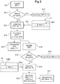
- step S30 the processor 10 sends on the bus BS3 a request for an instruction INF1 which is present within a group of instructions LM1 which it is assumed in this example, to occupy a line of the external memory 17.
- the cache controller first checks in step S31 whether this instruction INF1 is already stored in a cache line of the cache memory 12.
- the cache controller supplies the instruction INF1 to the processor 10 (step S32).
- the cache controller sends a request to the first interface 111 so that the group of instructions LM1 occupying the line of memory 17 and containing the instruction INF1, is transmitted on the bus BS1 to this first interface 111, the instruction INF1 being transmitted first (step S33).
- step S34 the cache controller provides the instruction INF1 to the processor 10 on the bus BS3.
- step S35 the entire group of instructions LM1 is loaded into a buffer memory of the first interface 111.
- step S36 a second request for a second instruction INF2 which is this time stored within a second group of instructions LM2 that it is assumed in this example, to occupy a line LM2 in the internal memory 16.
- this part of memory containing the group LM2 is “cacheable”, that is to say intended to be also stored in the cache memory.
- the cache controller therefore checks in step S37 if there is a cache fault.
- the cache controller supplies the instruction INF2 to the processor 10 (step S38).
- the second interface 112 will read the internal memory 16 so as to obtain on the bus BS2 the group of instructions LM2 containing the instruction INF2 (step S39).
- the cache controller supplies this instruction INF2 in step S40 to the processor 10, even if the loading of the information group LM1 is still in progress in the buffer memory of the first interface 111 (step S35).
- this instruction INF2 triggers an interrupt program, this can be carried out immediately without waiting for the loading of the information group LM1 to finish in the buffer memory of the interface 111.
- the entire information group LM2 is loaded into the buffer memory of the interface 112 (step S41), for the purpose of subsequent storage in a cache line of the cache memory.
- the interface sends an indication to the cache control circuit 114.
- step S42 this will then load this group of information LM1 into a cache line LC1 of the cache memory 12.
- this interface When the latter is loaded (step S41) into the buffer memory of the interface 112, this interface sends an indication to the cache control circuit which then loads the group of instructions LM2 into a cache line LC2 of the cache memory 12 (step S43).
- the cache line LC1 can be identical to the cache line LC2.
- the instruction group LM1 and the instruction group LM2 are intended to be stored in the same cache line, for example the cache line LC1.
- step S35 the loading of the instruction group LM1 is carried out in the buffer memory of the first interface 111 (step S35) as indicated above.
- step S41 there is a loading in progress of the group of instructions LM2 containing the second instruction INF2 required by the processor, in the buffer of the second interface 112 (step S41).
- the cache control circuit 114 will then load the instruction group LM2 in the cache line LC1 (step S43).
- the cache controller sends an instruction to abort the loading in progress of the group of instructions LM1 in the buffer memory of l 'interface 111 (step S50).
- the invention therefore makes it possible to manage in parallel accesses to different memories containing for example instructions to be executed by the processor, and not to penalize the execution of an interrupt program stored in a memory, internal for example, while a series of instructions from another memory, external for example, is being loaded into a buffer memory in order to load it into a cache line of the cache memory.
- the invention offers an advantageous replacement policy in cache memory. Indeed, in the case where a second series of instructions resulting from a second request subsequent to a first request, is ready to be loaded into said cache line before the first series of instructions resulting from the previous request, it is provided for an abortion of the process leading to the loading of the first series of instructions in said cache line.
Abstract
Après un premier défaut de cache consécutif à une première requête d'une première instruction (INF1) émanant du processeur, on fournit au processeur la première information issue d'une première mémoire (17). Après une deuxième requête d'une deuxième instruction (INF2) émanant du processeur postérieure à la première requête, on fournit au processeur (10) la deuxième information issue d'une deuxième mémoire (16) même si un groupe d'informations (LM1) contenant la première instruction est en cours de transfert depuis la première mémoire (17) en vue de son chargement dans une ligne de cache de la mémoire cache (12).After a first cache fault consecutive to a first request for a first instruction (INF1) emanating from the processor, the processor is supplied with the first information item coming from a first memory (17). After a second request of a second instruction (INF2) emanating from the processor subsequent to the first request, the processor (10) is supplied with the second information item from a second memory (16) even if a group of information items (LM1) containing the first instruction is being transferred from the first memory (17) for loading into a cache line of the cache memory (12).
Description
Des modes de mise en oeuvre et de réalisation de l'invention concernent les processeurs, et notamment la gestion de la fourniture d'informations, par exemple des instructions, à ces processeurs en particulier lorsqu'une partie du logiciel à exécuter par le processeur se situe dans une mémoire externe et que cette partie de logiciel est amenée à être stockée dans une mémoire cache de façon à optimiser le temps d'exécution du code.Embodiments and embodiments of the invention relate to processors, and in particular the management of the supply of information, for example instructions, to these processors in particular when part of the software to be executed by the processor is located in an external memory and that this part of software is brought to be stored in a cache memory so as to optimize the execution time of the code.
Il existe un besoin de ne pas pénaliser le temps d'exécution d'un groupe d'instructions, par exemple un programme d'interruption, situé dans une autre mémoire, par exemple une mémoire flash interne, alors qu'une ligne d'instructions contenant une instruction précédente requise par le processeur et stockée dans la mémoire externe, est en cours de chargement en vue de son stockage dans une mémoire cache.There is a need not to penalize the execution time of a group of instructions, for example an interrupt program, located in another memory, for example an internal flash memory, while a line of instructions containing a previous instruction required by the processor and stored in the external memory, is being loaded for storage in a cache memory.
Selon un aspect, il est proposé un procédé de gestion de la fourniture d'informations à un processeur.According to one aspect, a method of managing the supply of information to a processor is proposed.
Le terme « information » s'entend dans un sens très large incluant par exemple des instructions, mais également éventuellement des données nécessaires à ces instructions telles que des notations (« litteral » en langue anglaise) représentant une valeur fixe dans un code source.The term "information" is understood in a very broad sense including for example instructions, but also possibly data necessary for these instructions such as notations ("litteral" in English) representing a fixed value in a source code.
Le processeur coopère avec un ensemble de mémoires comportant au moins
une mémoire cache,
une première mémoire, par exemple une mémoire externe, stockant au moins une première information, par exemple une instruction, au sein d'un premier groupe d'informations, et
une deuxième mémoire, par exemple une mémoire interne telle qu'une mémoire flash, stockant au moins une deuxième information, par exemple une ou plusieurs instructions d'un programme d'interruption, au sein d'un deuxième groupe d'informations.The processor cooperates with a set of memories comprising at least
a cache memory,
a first memory, for example an external memory, storing at least a first piece of information, for example an instruction, within a first group of information, and
a second memory, for example an internal memory such as a flash memory, storing at least a second piece of information, for example one or more instructions of an interrupt program, within a second group of information.
Un groupe d'informations peut comprendre plusieurs bits organisés typiquement en plusieurs mots, par exemple 4 mots de 64 bits.An information group can comprise several bits typically organized in several words, for example 4 words of 64 bits.
En fonction de la technologie utilisée pour la mémoire stockant ce groupe d'informations, celui-ci peut occuper par exemple une portion de ligne ou une ligne complète ou plusieurs lignes de cette mémoire.Depending on the technology used for the memory storing this group of information, it can occupy for example a portion of a line or a complete line or several lines of this memory.
Le procédé comprend,
- après un premier défaut de cache consécutif à une première requête de ladite première information émanant du processeur, une première fourniture au processeur de la première information issue de la première mémoire, puis,
- après une deuxième requête de ladite deuxième information émanant du processeur, une deuxième fourniture au processeur de la deuxième information issue de la deuxième mémoire, même si le premier groupe d'informations est en cours de transfert depuis la première mémoire en vue de son chargement dans la mémoire cache.
- after a first cache fault consecutive to a first request for said first information originating from the processor, a first supply to the processor of the first information originating from the first memory, then,
- after a second request for said second information from the processor, a second supply to the processor of second information from the second memory, even if the first group of information is being transferred from the first memory for loading into cache memory.
Ainsi, même si ce transfert de ce premier groupe d'informations prend plusieurs centaines de cycles du signal d'horloge cadençant le processeur, le programme d'interruption peut être effectué en temps réel.Thus, even if this transfer of this first group of information takes several hundred cycles of the clock signal clocking the processor, the interrupt program can be carried out in real time.
Le chargement dans une mémoire cache s'effectue typiquement dans un emplacement de cette mémoire cache communément désigné par l'homme du métier sous la dénomination « ligne de cache ». Cette ligne de cache comporte un ensemble d'emplacements mémoire destinés à stocker un groupe de bits et représente l'élément indivisible auquel on va accéder pour déterminer si l'on a ou non un défaut de cache (« miss » en langue anglaise) ou pour y stocker un nouveau groupe de bits émanant d'une autre mémoire à la suite d'un défaut de cache.The loading into a cache memory is typically carried out in a location of this cache memory commonly designated by a person skilled in the art under the name "cache line". This cache line comprises a set of memory locations intended for storing a group of bits and represents the indivisible element which will be accessed to determine whether or not there is a cache defect (“miss” in English) or to store a new group of bits from another memory following a cache fault.
En fonction de la technologie utilisée et de la taille de ligne de cache, une mémoire cache peut comporter une seule mémoire vive ou plusieurs mémoires vives accessibles en parallèle et la ligne de cache peut se situer au sein d'une portion de ligne ou d'une ligne ou de plusieurs lignes de la mémoire vive unique ou au sein de plusieurs lignes dans plusieurs mémoires vives.Depending on the technology used and the size of the cache line, a cache memory can comprise a single random access memory or several random access memories accessible in parallel and the cache line can be located within a portion of line or a line or several lines of the single random access memory or within several lines in several random access memories.
Le deuxième groupe d'informations dans lequel se situe la deuxième information, peut être ou non destiné à être stocké dans la mémoire cache, c'est-à-dire qu'il peut être « cachable » ou « non cachable ».The second group of information in which the second information is located may or may not be intended to be stored in the cache memory, that is to say it may be "cacheable" or "non-cacheable".
Si la deuxième information est destinée à être stockée dans la mémoire cache (c'est-à-dire si elle est « cachable »), alors le procédé comprend en outre un deuxième défaut de cache consécutif à la deuxième requête. En d'autres termes, la fourniture de la deuxième information issue de la deuxième mémoire fait suite à un défaut de cache.If the second information is intended to be stored in the cache memory (that is to say if it is “cacheable”), then the method also comprises a second cache fault consecutive to the second request. In other words, the supply of the second information item coming from the second memory follows a cache fault.
Selon un mode de mise en oeuvre, on peut prévoir un contrôleur de cache couplé entre le processeur et l'ensemble de mémoires, et la première fourniture de la première information et la deuxième fourniture de la deuxième information peuvent être alors respectivement effectuées sur deux bus distincts reliant respectivement la première mémoire et la deuxième mémoire au contrôleur de cache et sur un troisième bus reliant le contrôleur de cache et le processeur.According to one embodiment, a cache controller can be provided coupled between the processor and the set of memories, and the first supply of the first information and the second supply of the second information can then be respectively carried out on two buses separate connecting the first memory and the second memory respectively to the cache controller and on a third bus connecting the cache controller and the processor.
Selon un mode de mise en oeuvre, si le deuxième groupe d'informations est prêt à être chargé dans une ligne de cache de la mémoire cache avant que le premier groupe d'informations soit prêt à être chargé dans cette même ligne de cache (alors que le processeur a d'abord fait la requête de la première information puis la requête de la deuxième information) on interdit alors le chargement du premier groupe d'informations dans ladite ligne de cache.According to one embodiment, if the second group of information is ready to be loaded into a cache line of the cache memory before the first group of information is ready to be loaded into this same line of cache (then that the processor has first made the request for the first information then the request for the second information) the loading of the first group of information is then prohibited in said cache line.
En d'autres termes, si le premier groupe d'informations et le deuxième groupe d'informations sont destinés à être stockés dans une même ligne de cache, on va interdire le chargement du premier groupe d'informations dans cette ligne de cache si le deuxième groupe d'informations qui a fait l'objet d'une requête postérieure, est prêt à être stocké dans la ligne de cache avant que le premier groupe d'informations ne soit prêt à y être stocké.In other words, if the first group of information and the second group of information are intended to be stored in the same cache line, we will prohibit the loading of the first group of information in this cache line if the second group that was later requested, is ready to be stored in the cache line before the first group of information is ready to be stored there.
En effet dans le cas d'une politique de remplacement déterministe prévoyant par exemple que les informations émanant de la deuxième mémoire sont prioritaires, il est souhaitable de respecter cette priorité afin de ne pas casser le déterminisme du procédé.Indeed, in the case of a deterministic replacement policy providing for example that the information emanating from the second memory has priority, it is desirable to respect this priority so as not to break the determinism of the process.
Aussi ce mode de mise en oeuvre évite d'écraser dans la ligne de cache, des informations prioritaires par des informations qui sont moins prioritaires.Also this mode of implementation avoids overwriting in the cache line, priority information by information which is less priority.
Comme indiqué ci-avant, la première information peut comporter au moins une instruction à exécuter par le processeur.As indicated above, the first information item may include at least one instruction to be executed by the processor.
Par ailleurs, la deuxième information peut comporter au moins une instruction d'un programme d'interruption.Furthermore, the second piece of information may include at least one instruction from an interrupt program.
Selon un autre aspect, il est proposé un système, comprenant
un processeur,
un ensemble de mémoire configuré pour coopérer avec le processeur et comportant au moins une mémoire cache, une première mémoire configurée pour stocker au moins une première information au sein d'un premier groupe d'informations et une deuxième mémoire configurée pour stocker au moins une deuxième information au sein d'un deuxième groupe d'informations, et
des moyens de contrôle configurés pour :
- après une première requête de ladite première information émanant du processeur, effectuer une première fourniture au processeur de la première information issue de la première mémoire, puis
- après une deuxième requête de ladite deuxième information émanant du processeur, effectuer une deuxième fourniture au processeur de la deuxième information issue de la deuxième mémoire, même si le premier groupe d'informations est en cours de transfert depuis la première mémoire en vue de son chargement dans la mémoire cache, typiquement dans une ligne de cache de cette mémoire cache.
a processor,
a memory assembly configured to cooperate with the processor and comprising at least one cache memory, a first memory configured to store at least one first information within a first group of information and a second memory configured to store at least a second information within a second group of information, and
control means configured for:
- after a first request for said first information from the processor, make a first supply to the processor of the first information from the first memory, then
- after a second request for said second information from the processor, make a second supply to the processor of the second information from the second memory, even if the first group of information is being transferred from the first memory for loading in the cache, typically in a cache line of this cache memory.
Selon un mode de réalisation, dans le cas où la deuxième information est « cachable », les moyens de contrôle sont configurés pour effectuer ladite deuxième fourniture après un deuxième défaut de cache consécutif à ladite deuxième requête.According to one embodiment, in the case where the second item of information is "cacheable", the control means are configured to carry out said second supply after a second cache fault consecutive to said second request.
Selon un mode de réalisation, les moyens de contrôle comprennent
- un contrôleur de cache couplé entre le processeur et l'ensemble de mémoires, et possédant au moins une première interface, une deuxième interface et une troisième interface,
- un premier bus couplé entre la première interface et la première mémoire,
- un deuxième bus couplé entre la deuxième interface et la deuxième mémoire,
- un troisième bus couplé entre la troisième interface et le processeur,
- a cache controller coupled between the processor and the set of memories, and having at least a first interface, a second interface and a third interface,
- a first bus coupled between the first interface and the first memory,
- a second bus coupled between the second interface and the second memory,
- a third bus coupled between the third interface and the processor,
Le contrôleur de cache est avantageusement configuré pour fournir la première information délivrée par la première mémoire sur le premier bus, au processeur via la troisième interface et le troisième bus, et pour fournir la deuxième information délivrée par la deuxième mémoire sur le deuxième bus, au processeur via la troisième interface et le troisième bus.The cache controller is advantageously configured to provide the first information delivered by the first memory on the first bus, to the processor via the third interface and the third bus, and to provide the second information delivered by the second memory on the second bus, to the processor via the third interface and the third bus.
Selon un mode de réalisation, les moyens de contrôle sont configurés pour, si le deuxième groupe d'informations est prêt à être chargé dans une ligne de cache de la mémoire cache avant que le premier groupe d'informations soit prêt à être chargé dans cette même ligne de cache, interdire le chargement du premier groupe.According to one embodiment, the control means are configured for, if the second group of information is ready to be loaded in a cache line of the cache memory before the first group of information is ready to be loaded in this same cache line, prohibit loading of the first group.
Plus précisément, dans ce cas, selon un mode de réalisation, la première interface comporte une mémoire tampon configurée pour stocker le premier groupe d'informations extrait de la première mémoire et le contrôleur de cache est configuré pour faire avorter le processus de stockage du premier groupe d'informations.More specifically, in this case, according to one embodiment, the first interface includes a buffer memory configured to store the first group of information extracted from the first memory and the cache controller is configured to abort the storage process of the first information group.
Comme indiqué ci-avant, la première information peut comporter au moins une instruction à exécuter par le processeur tandis que la deuxième information peut comporter au moins une instruction d'un programme d'interruption.As indicated above, the first information can include at least one instruction to be executed by the processor while the second information can include at least one instruction from an interrupt program.
Le système peut comprendre un microcontrôleur incorporant le processeur, la mémoire cache, la deuxième mémoire et le contrôleur de cache, la première mémoire étant une mémoire externe au microcontrôleur.The system may include a microcontroller incorporating the processor, the cache memory, the second memory and the cache controller, the first memory being a memory external to the microcontroller.
D'autres avantages et caractéristiques de l'invention apparaîtront à l'examen de la description détaillée de modes de mise en oeuvre et de réalisation, nullement limitatifs, et des dessins annexés sur lesquels :
- les
figures 1 à 5 illustrent schématiquement des modes de réalisation et de mise en oeuvre de l'invention.
- the
Figures 1 to 5 schematically illustrate embodiments and implementation of the invention.
Sur la
Ce microcontrôleur comporte une unité centrale de calcul ou processeur 10, ainsi qu'un ensemble de mémoires comportant ici une mémoire 17, externe au microcontrôleur, une mémoire interne 16, par exemple une mémoire flash, et une autre mémoire interne 15, par exemple une mémoire vive (mémoire RAM).This microcontroller comprises a central computing unit or
La mémoire externe 17 est couplée à un contrôleur de mémoire 14 de structure classique.The
Le microcontrôleur 1 comporte par ailleurs une mémoire cache 12, de structure classique, par exemple une mémoire 2-associative (2-ways-associative) couplée à un contrôleur de cache 11.The
Le contrôleur de cache 11 est couplé au contrôleur de mémoire 14 à la mémoire 15 et à la mémoire 16 par un circuit d'interconnexion 13 comportant des ports d'entrée et des ports de sortie.The
La structure d'un tel circuit d'interconnexion, qui est en général un circuit d'interconnexion multicouches, ainsi que le protocole permettant l'échange et le routage des transactions à l'intérieur du circuit d'interconnexion sont bien connus de l'homme du métier.The structure of such an interconnection circuit, which is generally a multilayer interconnection circuit, as well as the protocol allowing the exchange and routing of transactions to the interior of the interconnection circuit are well known to those skilled in the art.
Celui-ci pourra par exemple se référer notamment :
- à l'article de
Venkateswara Rao et autres intitulé « A Frame work on AMBA bus based Communication Architecture to improve the Real Time Computing Performance in MPSoC », International Journal of Computer Applications (0975-8887), Volume 91 - N° 5, Avril 2014
ou - à une présentation générale de ces circuits d'interconnexion effectuée en 2015 par A. Gerstlauer et disponible à l'adresse internet http://users.ece.utexas.edu/∼gerstl/ee382v_f14/lectures/lecture_12.pdf.
- to the article by
Venkateswara Rao and others entitled “A Frame work on AMBA bus based Communication Architecture to improve the Real Time Computing Performance in MPSoC”, International Journal of Computer Applications (0975-8887), Volume 91 - N ° 5, April 2014
or - to a general presentation of these interconnection circuits carried out in 2015 by A. Gerstlauer and available at the internet address http://users.ece.utexas.edu/∼gerstl/ee382v_f14/lectures/lecture_12.pdf .
Par ailleurs, à titre indicatif mais non limitatif, on peut utiliser par exemple le circuit d'interconnexion commercialisé par la société ARM sous la référence NIC-400 (version R0p3).Furthermore, for information but not limitation, one can use for example the interconnection circuit marketed by the company ARM under the reference NIC-400 (version R0p3).
Le circuit d'interconnexion 13 est connecté au contrôleur de cache 11 par deux bus BS1 et BS2.The
Le contrôleur de cache est relié par ailleurs au microprocesseur par un troisième bus BS3 ainsi que par un quatrième bus BS4 qui, comme on le verra plus en détail, permettra une configuration des registres du contrôleur de cache.The cache controller is also connected to the microprocessor by a third bus BS3 as well as by a fourth bus BS4 which, as will be seen in more detail, will allow configuration of the registers of the cache controller.
Les différents bus peuvent être de toute structure classique, et par exemple des bus AHB utilisant un protocole décrit par exemple dans le document AMBA 3 AHB-Lite Protocol V1.0 Spécification, de la société ARM (2001, 2006).The various buses can be of any conventional structure, and for example AHB buses using a protocol described for example in the document AMBA 3 AHB-Lite Protocol V1.0 Specification, from the company ARM (2001, 2006).
Le contrôleur de cache 11, couplé entre le processeur 10 et l'ensemble de mémoires 15, 16 et 17, le premier bus BS1, le deuxième bus BS2, le troisième bus BS3 forment ici des moyens de contrôle configurés pour
- après une première requête d'une première information, par exemple une première instruction, émanant du processeur 10, effectuer une première fourniture au processeur 10 de la première instruction issue de la première mémoire 17, puis,
- après une deuxième requête d'une deuxième instruction émanant du processeur 10, effectuer une deuxième fourniture au processeur 10 de cette deuxième instruction issue de la deuxième mémoire 16 même si le groupe d'instructions dans lequel figure la première instruction est en cours de transfert depuis la première mémoire 17 en vue de son chargement dans une ligne de cache de la mémoire
cache 12.
- after a first request for first information, for example a first instruction, emanating from the
processor 10, make a first supply to theprocessor 10 of the first instruction coming from thefirst memory 17, then, - after a second request for a second instruction from the
processor 10, make a second supply to theprocessor 10 of this second instruction from thesecond memory 16 even if the group of instructions in which the first instruction appears is being transferred from thefirst memory 17 for loading into a cache line of thecache memory 12.
On reviendra plus en détail ci-après sur un exemple de mise en oeuvre d'un tel procédé.We will return in more detail below to an example of implementation of such a method.
Si l'on se réfère maintenant plus particulièrement à la
Le contrôleur de cache comporte également une interface de registre 116 couplée au bus BS4.The cache controller also includes a
La troisième interface 113 comporte une machine d'état destinée à gérer le dialogue avec le bus relié au processeur 10.The
Cette interface 113 reçoit les requêtes en provenance du processeur comportant les adresses des informations (instructions) requises en mémoire, et fournit les instructions au processeur lorsqu'elles sont disponibles.This
La première interface 111 est configurée pour recevoir les requêtes d'instructions émanant du processeur 10 à destination de la mémoire externe 17 et pour fournir les instructions correspondantes au processeur 10.The
En outre, lorsqu'une instruction fait partie d'un groupe d'instructions au sein de la première mémoire, la première interface 111 comporte une mémoire tampon configurée pour stocker ce groupe d'instructions extrait de la mémoire 17 puis, lorsque le stockage est terminé, envoyer une indication à un circuit de contrôle de cache 114 qui commande l'écriture et la lecture dans la mémoire cache 12.In addition, when an instruction is part of a group of instructions within the first memory, the
La deuxième interface 112 présente une structure équivalente à celle de la première interface 111 et est configurée pour cette fois-ci recevoir les requêtes d'instructions émanant du processeur 10 à destination de la mémoire interne 16 et pour renvoyer les instructions au processeur 10.The
Les deux interfaces 111 et 112 comportent également des machines d'état.The two
Comme indiqué ci-avant l'interface 116 permet de configurer les registres du contrôleur de cache en réponse à une indication de configuration émanant du processeur, et permet notamment de désigner en fonction de l'adresse associée à une requête du processeur, dans quelle mémoire l'information ou l'instruction correspondante est stockée.As indicated above, the
On se réfère maintenant plus particulièrement aux
Sur la
Le contrôleur de cache vérifie tout d'abord dans l'étape S31 si cette instructions INF1 est déjà stockée dans une ligne de cache de la mémoire cache 12.The cache controller first checks in step S31 whether this instruction INF1 is already stored in a cache line of the
Si l'on n'a pas de défaut de cache, c'est-à-dire si cette instruction INF1 est déjà stockée dans la ligne de cache de la mémoire cache, alors le contrôleur de cache fournit l'instruction INF1 au processeur 10 (étape S32).If there is no cache fault, that is to say if this instruction INF1 is already stored in the cache line of the cache memory, then the cache controller supplies the instruction INF1 to the processor 10 (step S32).
Dans le cas où l'on a un défaut de cache c'est-à-dire si l'instruction INF1 n'est pas stockée dans une ligne de cache de la mémoire cache, alors le contrôleur de cache envoie une requête à la première interface 111 de façon que le groupe d'instructions LM1 occupant la ligne de la mémoire 17 et contenant l'instruction INF1, soit transmise sur le bus BS1 à cette première interface 111, l'instruction INF1 étant transmise en premier (étape S33).In the case where there is a cache fault, that is to say if the instruction INF1 is not stored in a cache line of the cache memory, then the cache controller sends a request to the
Puis, dans l'étape S34, le contrôleur de cache fournit l'instruction INF1 au processeur 10 sur le bus BS3.Then, in step S34, the cache controller provides the instruction INF1 to the
Parallèlement, l'ensemble du groupe d'instructions LM1 est chargé dans une mémoire tampon de la première interface 111 (étape S35).In parallel, the entire group of instructions LM1 is loaded into a buffer memory of the first interface 111 (step S35).
On suppose également que postérieurement à la requête de l'instruction INF1, le processeur émet dans l'étape S36 une deuxième requête d'une deuxième instruction INF2 qui est cette fois-ci stockée au sein d'un deuxième groupe d'instructions LM2 que l'on suppose dans cet exemple, occuper une ligne LM2 dans la mémoire interne 16.It is also assumed that after the request for the instruction INF1, the processor transmits in step S36 a second request for a second instruction INF2 which is this time stored within a second group of instructions LM2 that it is assumed in this example, to occupy a line LM2 in the
Dans cet exemple, on suppose que cette partie de mémoire contenant le groupe LM2 est « cachable » c'est-à-dire destinée à être également stockée dans la mémoire cache.In this example, it is assumed that this part of memory containing the group LM2 is “cacheable”, that is to say intended to be also stored in the cache memory.
Le contrôleur de cache vérifie donc dans l'étape S37 si l'on est en présence d'un défaut de cache.The cache controller therefore checks in step S37 if there is a cache fault.
En l'absence de défaut de cache, c'est-à-dire si l'instruction INF2 est déjà présente dans la mémoire cache, le contrôleur de cache fournit l'instruction INF2 au processeur 10 (étape S38).In the absence of a cache fault, that is to say if the instruction INF2 is already present in the cache memory, the cache controller supplies the instruction INF2 to the processor 10 (step S38).
Par contre, en présence d'un défaut de cache, la deuxième interface 112 va lire la mémoire interne 16 de façon à obtenir sur le bus BS2 le groupe d'instructions LM2 contenant l'instruction INF2 (étape S39).On the other hand, in the presence of a cache fault, the
Là encore, l'instruction INF2 est fournie en premier à l'interface 112.Again, the instruction INF2 is supplied first to the
Et, le contrôleur de cache fournit cette instruction INF2 dans l'étape S40 au processeur 10, et ce même si le chargement du groupe d'informations LM1 est toujours en cours dans la mémoire tampon de la première interface 111 (étape S35).And, the cache controller supplies this instruction INF2 in step S40 to the
De ce fait, si cette instruction INF2 déclenche un programme d'interruption, celui-ci peut être effectué immédiatement sans attendre la fin du chargement du groupe d'information LM1 dans la mémoire tampon de l'interface 111.Therefore, if this instruction INF2 triggers an interrupt program, this can be carried out immediately without waiting for the loading of the information group LM1 to finish in the buffer memory of the
Puis, l'ensemble du groupe d'informations LM2 est chargé dans la mémoire tampon de l'interface 112 (étape S41), aux fins d'un stockage ultérieur dans une ligne de cache de la mémoire cache.Then, the entire information group LM2 is loaded into the buffer memory of the interface 112 (step S41), for the purpose of subsequent storage in a cache line of the cache memory.
Ceci est illustré plus en détail sur la
Plus précisément, une fois le chargement du groupe d'informations LM1 effectué dans la mémoire tampon de la première interface 111 (étape S35), l'interface émet une indication à destination du circuit de contrôle de cache 114.More precisely, once the information group LM1 has been loaded into the buffer memory of the first interface 111 (step S35), the interface sends an indication to the
Celui-ci va alors dans l'étape S42, charger ce groupe d'informations LM1 dans une ligne de cache LC1 de la mémoire cache 12.In step S42, this will then load this group of information LM1 into a cache line LC1 of the
Le même processus est effectué en ce qui concerne le groupe d'informations LM2.The same process is performed for the LM2 information group.
Lorsque celui-ci est chargé (étape S41) dans la mémoire tampon de l'interface 112, cette interface émet une indication à destination du circuit de contrôle de cache qui charge alors le groupe d'instructions LM2 dans une ligne de cache LC2 de la mémoire cache 12 (étape S43).When the latter is loaded (step S41) into the buffer memory of the
Lorsque les lignes de cache LC1 et LC2 sont différentes, il n'y a pas de problème.When the LC1 and LC2 cache lines are different, there is no problem.
Par contre, dans certains cas, la ligne de cache LC1 peut être identique à la ligne de cache LC2.On the other hand, in certain cases, the cache line LC1 can be identical to the cache line LC2.
En d'autres termes, le groupe d'instructions LM1 et le groupe d'instructions LM2 sont destinés à être stockés dans une même ligne de cache, par exemple la ligne de cache LC1.In other words, the instruction group LM1 and the instruction group LM2 are intended to be stored in the same cache line, for example the cache line LC1.
Ceci est illustré sur la
Aussi, à la suite de la première requête de l'instruction INF1, le chargement du groupe d'instructions LM1 est effectué dans la mémoire tampon de la première interface 111 (étape S35) comme indiqué ci-avant.Also, following the first request of the instruction INF1, the loading of the instruction group LM1 is carried out in the buffer memory of the first interface 111 (step S35) as indicated above.
Et ce groupe d'instructions LM1 est destiné ensuite à être chargé dans la ligne de cache LC1 de la mémoire cache 12.And this group of instructions LM1 is then intended to be loaded into the cache line LC1 of the
Parallèlement, il y a un chargement en cours du groupe d'instructions LM2 contenant la deuxième instruction INF2 requise par le processeur, dans la mémoire tampon de la deuxième interface 112 (étape S41).In parallel, there is a loading in progress of the group of instructions LM2 containing the second instruction INF2 required by the processor, in the buffer of the second interface 112 (step S41).
Et, si le chargement S41 est terminé alors que le chargement S35 est alors en cours, le circuit de contrôle de cache 114 va alors charger le groupe d'instructions LM2 dans la ligne de cache LC1 (étape S43).And, if the loading S41 is finished while the loading S35 is then in progress, the
Et, de façon à ce que ce groupe d'instructions LM2 ne soit pas écrasé par le groupe d'instructions LM1 le contrôleur de cache envoie une instruction d'avortement du chargement en cours du groupe d'instructions LM1 dans la mémoire tampon de l'interface 111 (étape S50).And, so that this group of instructions LM2 is not overwritten by the group of instructions LM1 the cache controller sends an instruction to abort the loading in progress of the group of instructions LM1 in the buffer memory of l 'interface 111 (step S50).
L'invention permet donc de gérer en parallèle des accès à des mémoires différentes contenant par exemple des instructions à exécuter par le processeur, et de ne pas pénaliser l'exécution d'un programme d'interruption stocké dans une mémoire, interne par exemple, alors qu'une série d'instructions issues d'une autre mémoire, externe par exemple, est en cours de chargement dans une mémoire tampon en vue de son chargement dans une ligne de cache de la mémoire cache.The invention therefore makes it possible to manage in parallel accesses to different memories containing for example instructions to be executed by the processor, and not to penalize the execution of an interrupt program stored in a memory, internal for example, while a series of instructions from another memory, external for example, is being loaded into a buffer memory in order to load it into a cache line of the cache memory.
Ceci s'applique que le programme d'interruption soit « cachable » ou non.This applies whether the interrupt program is "cacheable" or not.
Par ailleurs, dans le cas où deux séries d'instructions respectivement stockées par exemple dans deux lignes de mémoires des deux mémoires sont « cachables » et destinées à être stockées dans une même ligne de cache, l'invention offre une politique avantageuse de remplacement dans la mémoire cache. En effet, dans le cas où une deuxième série d'instructions résultant d'une deuxième requête postérieure à une première requête, est prête à être chargée dans ladite ligne de cache avant la première série d'instructions résultant de la requête antérieure, il est prévu un avortement du processus conduisant au chargement de la première série d'instructions dans ladite ligne de cache.Furthermore, in the case where two series of instructions respectively stored for example in two lines of memories of the two memories are "concealable" and intended to be stored in the same cache line, the invention offers an advantageous replacement policy in cache memory. Indeed, in the case where a second series of instructions resulting from a second request subsequent to a first request, is ready to be loaded into said cache line before the first series of instructions resulting from the previous request, it is provided for an abortion of the process leading to the loading of the first series of instructions in said cache line.
Claims (14)
le contrôleur de cache (11) étant configuré pour fournir la première information délivrée par la première mémoire sur le premier bus au processeur via la troisième interface et le troisième bus, et pour fournir la deuxième information délivrée par la deuxième mémoire sur le deuxième bus au processeur via la troisième interface et le troisième bus.
the cache controller (11) being configured to provide the first information delivered by the first memory on the first bus to the processor via the third interface and the third bus, and to provide the second information delivered by the second memory on the second bus to the processor via the third interface and the third bus.
Applications Claiming Priority (1)
| Application Number | Priority Date | Filing Date | Title |
|---|---|---|---|
| FR1858771A FR3086409A1 (en) | 2018-09-26 | 2018-09-26 | METHOD FOR MANAGING THE PROVISION OF INFORMATION, PARTICULARLY INSTRUCTIONS, TO A MICROPROCESSOR AND CORRESPONDING SYSTEM |
Publications (1)
| Publication Number | Publication Date |
|---|---|
| EP3629185A1 true EP3629185A1 (en) | 2020-04-01 |
Family
ID=65243871
Family Applications (1)
| Application Number | Title | Priority Date | Filing Date |
|---|---|---|---|
| EP19196986.4A Pending EP3629185A1 (en) | 2018-09-26 | 2019-09-12 | Method for managing the supply of information, in particular of instructions, with a microprocessor and corresponding system |
Country Status (4)
| Country | Link |
|---|---|
| US (1) | US11275589B2 (en) |
| EP (1) | EP3629185A1 (en) |
| CN (2) | CN211906256U (en) |
| FR (1) | FR3086409A1 (en) |
Families Citing this family (1)
| Publication number | Priority date | Publication date | Assignee | Title |
|---|---|---|---|---|
| FR3086409A1 (en) * | 2018-09-26 | 2020-03-27 | Stmicroelectronics (Grenoble 2) Sas | METHOD FOR MANAGING THE PROVISION OF INFORMATION, PARTICULARLY INSTRUCTIONS, TO A MICROPROCESSOR AND CORRESPONDING SYSTEM |
Citations (3)
| Publication number | Priority date | Publication date | Assignee | Title |
|---|---|---|---|---|
| WO2001050269A2 (en) * | 1999-12-30 | 2001-07-12 | Intel Corporation | A method and apparatus to perform a round robin and locking cache replacement scheme |
| US20100211742A1 (en) * | 2009-02-13 | 2010-08-19 | Sebastian Turullols | Conveying critical data in a multiprocessor system |
| US20110225369A1 (en) * | 2010-03-10 | 2011-09-15 | Park Jae-Un | Multiport data cache apparatus and method of controlling the same |
Family Cites Families (10)
| Publication number | Priority date | Publication date | Assignee | Title |
|---|---|---|---|---|
| US4811215A (en) * | 1986-12-12 | 1989-03-07 | Intergraph Corporation | Instruction execution accelerator for a pipelined digital machine with virtual memory |
| US5848432A (en) * | 1993-08-05 | 1998-12-08 | Hitachi, Ltd. | Data processor with variable types of cache memories |
| US5826109A (en) * | 1994-01-04 | 1998-10-20 | Intel Corporation | Method and apparatus for performing multiple load operations to the same memory location in a computer system |
| WO2003081454A2 (en) * | 2002-03-21 | 2003-10-02 | Pact Xpp Technologies Ag | Method and device for data processing |
| US8171225B2 (en) * | 2007-06-28 | 2012-05-01 | Intel Corporation | Cache for a multi thread and multi core system and methods thereof |
| EP2271989A1 (en) * | 2008-04-22 | 2011-01-12 | Nxp B.V. | Multiprocessing circuit with cache circuits that allow writing to not previously loaded cache lines |
| US8504777B2 (en) * | 2010-09-21 | 2013-08-06 | Freescale Semiconductor, Inc. | Data processor for processing decorated instructions with cache bypass |
| KR20130057890A (en) * | 2011-11-24 | 2013-06-03 | 시게이트 테크놀로지 인터내셔날 | Hybrid drive and data transfer method there-of |
| US11514001B2 (en) * | 2018-04-17 | 2022-11-29 | EMC IP Holding Company LLC | Concurrent computations operating on same data for CPU cache efficiency |
| FR3086409A1 (en) * | 2018-09-26 | 2020-03-27 | Stmicroelectronics (Grenoble 2) Sas | METHOD FOR MANAGING THE PROVISION OF INFORMATION, PARTICULARLY INSTRUCTIONS, TO A MICROPROCESSOR AND CORRESPONDING SYSTEM |
-
2018
- 2018-09-26 FR FR1858771A patent/FR3086409A1/en active Pending
-
2019
- 2019-09-12 EP EP19196986.4A patent/EP3629185A1/en active Pending
- 2019-09-17 US US16/573,299 patent/US11275589B2/en active Active
- 2019-09-25 CN CN201921606117.9U patent/CN211906256U/en not_active Withdrawn - After Issue
- 2019-09-25 CN CN201910912337.2A patent/CN110955386B/en active Active
Patent Citations (3)
| Publication number | Priority date | Publication date | Assignee | Title |
|---|---|---|---|---|
| WO2001050269A2 (en) * | 1999-12-30 | 2001-07-12 | Intel Corporation | A method and apparatus to perform a round robin and locking cache replacement scheme |
| US20100211742A1 (en) * | 2009-02-13 | 2010-08-19 | Sebastian Turullols | Conveying critical data in a multiprocessor system |
| US20110225369A1 (en) * | 2010-03-10 | 2011-09-15 | Park Jae-Un | Multiport data cache apparatus and method of controlling the same |
Non-Patent Citations (1)
| Title |
|---|
| "A Frame work on AMBA bus based Communication Architecture to improve the Real Time Computing Performance in MPSoC", INTERNATIONAL JOURNAL OF COMPUTER APPLICATIONS (0975-8887, vol. 91, no. 5, April 2014 (2014-04-01) |
Also Published As
| Publication number | Publication date |
|---|---|
| FR3086409A1 (en) | 2020-03-27 |
| CN110955386A (en) | 2020-04-03 |
| CN211906256U (en) | 2020-11-10 |
| CN110955386B (en) | 2023-09-01 |
| US11275589B2 (en) | 2022-03-15 |
| US20200097294A1 (en) | 2020-03-26 |
Similar Documents
| Publication | Publication Date | Title |
|---|---|---|
| US20190243765A1 (en) | Efficient work unit processing in a multicore system | |
| US10909064B2 (en) | Application architecture supporting multiple services and caching | |
| FR2881540A1 (en) | Input output cache memory usage method for computer system, involves assuring that prefetch locking indicator of cache memory line of cache memory associated to memory request is in locked condition, if memory request is not speculative | |
| EP1619590B1 (en) | Method for programming a system on a chip DMA controller and system on a chip therefore. | |
| US20230004527A1 (en) | Architecture for management of digital files across distributed network | |
| FR2677472A1 (en) | CONTROL UNIT FOR MEMORY SECOND LEVEL CACHE. | |
| CN108959455A (en) | Single page Web application implementation method, device, computer equipment and storage medium | |
| CN108780450A (en) | The Persistent Management based on server in user's space | |
| US11586672B2 (en) | Remote virtualized asset delivery and local provisioning | |
| US20160179672A1 (en) | Mirroring a cache having a modified cache state | |
| EP1739561A1 (en) | Cache consistency in a shared-memory multiprocessor system | |
| EP1607878A1 (en) | Method and computer program for managing a virtual address used to program a DMA controller and associated system on a chip. | |
| US20160342621A1 (en) | System and method of providing or executing layered resources | |
| EP3629185A1 (en) | Method for managing the supply of information, in particular of instructions, with a microprocessor and corresponding system | |
| FR2754925A1 (en) | ATOMIC OPERATION ON REMOTE MEMORY AND DEVICE FOR CARRYING OUT THIS OPERATION | |
| US9852077B2 (en) | Preserving user changes to a shared layered resource | |
| US10019191B2 (en) | System and method for protecting contents of shared layer resources | |
| US10795824B2 (en) | Speculative data return concurrent to an exclusive invalidate request | |
| US9665283B2 (en) | System and method of creating layered resources | |
| EP3557433A1 (en) | Method for managing the routing of transactions between at least one source device and at least one target device, for example a multiport memory, and corresponding system on a chip | |
| US8214597B2 (en) | Cache tentative read buffer | |
| US20200379906A1 (en) | Selective release-behind of file pages | |
| FR2674044A1 (en) | Arrangement for predicting an instruction address resulting from a branch in a digital data processing system | |
| US8825970B1 (en) | System and method for mounting a storage volume utilizing a block reference list | |
| EP3531419A1 (en) | Method for managing the routing transactions between source devices, at least one target device, for example a multiport memory, and corresponding system on a chip |
Legal Events
| Date | Code | Title | Description |
|---|---|---|---|
| PUAI | Public reference made under article 153(3) epc to a published international application that has entered the european phase |
Free format text: ORIGINAL CODE: 0009012 |
|
| STAA | Information on the status of an ep patent application or granted ep patent |
Free format text: STATUS: REQUEST FOR EXAMINATION WAS MADE |
|
| 17P | Request for examination filed |
Effective date: 20190912 |
|
| AK | Designated contracting states |
Kind code of ref document: A1 Designated state(s): AL AT BE BG CH CY CZ DE DK EE ES FI FR GB GR HR HU IE IS IT LI LT LU LV MC MK MT NL NO PL PT RO RS SE SI SK SM TR |
|
| AX | Request for extension of the european patent |
Extension state: BA ME |
|
| STAA | Information on the status of an ep patent application or granted ep patent |
Free format text: STATUS: EXAMINATION IS IN PROGRESS |
|
| 17Q | First examination report despatched |
Effective date: 20210714 |
|
| RIC1 | Information provided on ipc code assigned before grant |
Ipc: G06F 12/128 20160101ALN20230127BHEP Ipc: G06F 13/16 20060101ALI20230127BHEP Ipc: G06F 12/0855 20160101ALI20230127BHEP Ipc: G06F 9/48 20060101ALI20230127BHEP Ipc: G06F 12/0875 20160101ALI20230127BHEP Ipc: G06F 12/126 20160101AFI20230127BHEP |
|
| GRAP | Despatch of communication of intention to grant a patent |
Free format text: ORIGINAL CODE: EPIDOSNIGR1 |
|
| STAA | Information on the status of an ep patent application or granted ep patent |
Free format text: STATUS: GRANT OF PATENT IS INTENDED |
|
| RIC1 | Information provided on ipc code assigned before grant |
Ipc: G06F 12/128 20160101ALN20240124BHEP Ipc: G06F 13/16 20060101ALI20240124BHEP Ipc: G06F 12/0855 20160101ALI20240124BHEP Ipc: G06F 9/48 20060101ALI20240124BHEP Ipc: G06F 12/0875 20160101ALI20240124BHEP Ipc: G06F 12/126 20160101AFI20240124BHEP |
|
| INTG | Intention to grant announced |
Effective date: 20240208 |