EP3627569A1 - Method of manufacturing semiconductor element - Google Patents
Method of manufacturing semiconductor element Download PDFInfo
- Publication number
- EP3627569A1 EP3627569A1 EP19198198.4A EP19198198A EP3627569A1 EP 3627569 A1 EP3627569 A1 EP 3627569A1 EP 19198198 A EP19198198 A EP 19198198A EP 3627569 A1 EP3627569 A1 EP 3627569A1
- Authority
- EP
- European Patent Office
- Prior art keywords
- metal layer
- recess
- rough
- structure body
- layer
- Prior art date
- Legal status (The legal status is an assumption and is not a legal conclusion. Google has not performed a legal analysis and makes no representation as to the accuracy of the status listed.)
- Granted
Links
Images




Classifications
-
- H—ELECTRICITY
- H10—SEMICONDUCTOR DEVICES; ELECTRIC SOLID-STATE DEVICES NOT OTHERWISE PROVIDED FOR
- H10H—INORGANIC LIGHT-EMITTING SEMICONDUCTOR DEVICES HAVING POTENTIAL BARRIERS
- H10H20/00—Individual inorganic light-emitting semiconductor devices having potential barriers, e.g. light-emitting diodes [LED]
- H10H20/80—Constructional details
- H10H20/83—Electrodes
- H10H20/831—Electrodes characterised by their shape
- H10H20/8312—Electrodes characterised by their shape extending at least partially through the bodies
-
- H—ELECTRICITY
- H10—SEMICONDUCTOR DEVICES; ELECTRIC SOLID-STATE DEVICES NOT OTHERWISE PROVIDED FOR
- H10H—INORGANIC LIGHT-EMITTING SEMICONDUCTOR DEVICES HAVING POTENTIAL BARRIERS
- H10H20/00—Individual inorganic light-emitting semiconductor devices having potential barriers, e.g. light-emitting diodes [LED]
- H10H20/01—Manufacture or treatment
- H10H20/011—Manufacture or treatment of bodies, e.g. forming semiconductor layers
- H10H20/013—Manufacture or treatment of bodies, e.g. forming semiconductor layers having light-emitting regions comprising only Group III-V materials
- H10H20/0133—Manufacture or treatment of bodies, e.g. forming semiconductor layers having light-emitting regions comprising only Group III-V materials with a substrate not being Group III-V materials
- H10H20/01335—Manufacture or treatment of bodies, e.g. forming semiconductor layers having light-emitting regions comprising only Group III-V materials with a substrate not being Group III-V materials the light-emitting regions comprising nitride materials
-
- H—ELECTRICITY
- H10—SEMICONDUCTOR DEVICES; ELECTRIC SOLID-STATE DEVICES NOT OTHERWISE PROVIDED FOR
- H10H—INORGANIC LIGHT-EMITTING SEMICONDUCTOR DEVICES HAVING POTENTIAL BARRIERS
- H10H20/00—Individual inorganic light-emitting semiconductor devices having potential barriers, e.g. light-emitting diodes [LED]
- H10H20/80—Constructional details
- H10H20/81—Bodies
- H10H20/819—Bodies characterised by their shape, e.g. curved or truncated substrates
- H10H20/82—Roughened surfaces, e.g. at the interface between epitaxial layers
-
- H—ELECTRICITY
- H10—SEMICONDUCTOR DEVICES; ELECTRIC SOLID-STATE DEVICES NOT OTHERWISE PROVIDED FOR
- H10H—INORGANIC LIGHT-EMITTING SEMICONDUCTOR DEVICES HAVING POTENTIAL BARRIERS
- H10H20/00—Individual inorganic light-emitting semiconductor devices having potential barriers, e.g. light-emitting diodes [LED]
- H10H20/01—Manufacture or treatment
-
- H—ELECTRICITY
- H10—SEMICONDUCTOR DEVICES; ELECTRIC SOLID-STATE DEVICES NOT OTHERWISE PROVIDED FOR
- H10H—INORGANIC LIGHT-EMITTING SEMICONDUCTOR DEVICES HAVING POTENTIAL BARRIERS
- H10H20/00—Individual inorganic light-emitting semiconductor devices having potential barriers, e.g. light-emitting diodes [LED]
- H10H20/01—Manufacture or treatment
- H10H20/011—Manufacture or treatment of bodies, e.g. forming semiconductor layers
- H10H20/018—Bonding of wafers
-
- H—ELECTRICITY
- H10—SEMICONDUCTOR DEVICES; ELECTRIC SOLID-STATE DEVICES NOT OTHERWISE PROVIDED FOR
- H10H—INORGANIC LIGHT-EMITTING SEMICONDUCTOR DEVICES HAVING POTENTIAL BARRIERS
- H10H20/00—Individual inorganic light-emitting semiconductor devices having potential barriers, e.g. light-emitting diodes [LED]
- H10H20/80—Constructional details
- H10H20/81—Bodies
-
- H—ELECTRICITY
- H10—SEMICONDUCTOR DEVICES; ELECTRIC SOLID-STATE DEVICES NOT OTHERWISE PROVIDED FOR
- H10H—INORGANIC LIGHT-EMITTING SEMICONDUCTOR DEVICES HAVING POTENTIAL BARRIERS
- H10H20/00—Individual inorganic light-emitting semiconductor devices having potential barriers, e.g. light-emitting diodes [LED]
- H10H20/80—Constructional details
- H10H20/85—Packages
- H10H20/857—Interconnections, e.g. lead-frames, bond wires or solder balls
-
- H—ELECTRICITY
- H10—SEMICONDUCTOR DEVICES; ELECTRIC SOLID-STATE DEVICES NOT OTHERWISE PROVIDED FOR
- H10P—GENERIC PROCESSES OR APPARATUS FOR THE MANUFACTURE OR TREATMENT OF DEVICES COVERED BY CLASS H10
- H10P95/00—Generic processes or apparatus for manufacture or treatments not covered by the other groups of this subclass
- H10P95/90—Thermal treatments, e.g. annealing or sintering
-
- H—ELECTRICITY
- H10—SEMICONDUCTOR DEVICES; ELECTRIC SOLID-STATE DEVICES NOT OTHERWISE PROVIDED FOR
- H10W—GENERIC PACKAGES, INTERCONNECTIONS, CONNECTORS OR OTHER CONSTRUCTIONAL DETAILS OF DEVICES COVERED BY CLASS H10
- H10W20/00—Interconnections in chips, wafers or substrates
- H10W20/01—Manufacture or treatment
-
- H—ELECTRICITY
- H10—SEMICONDUCTOR DEVICES; ELECTRIC SOLID-STATE DEVICES NOT OTHERWISE PROVIDED FOR
- H10H—INORGANIC LIGHT-EMITTING SEMICONDUCTOR DEVICES HAVING POTENTIAL BARRIERS
- H10H20/00—Individual inorganic light-emitting semiconductor devices having potential barriers, e.g. light-emitting diodes [LED]
- H10H20/01—Manufacture or treatment
- H10H20/032—Manufacture or treatment of electrodes
Definitions
- the present disclosure relates to a method of manufacturing a semiconductor element.
- Japanese Patent Publication No. 2016-174018 describes a method of manufacturing a semiconductor element including a step of bonding two members.
- a member having a surface with a recess is bonded to another member.
- a technique that allows for simplifying manufacturing steps and reducing manufacturing cost in a method of manufacturing a semiconductor element including such a bonding step would be desirable.
- the present disclosure includes the following inventions.
- the present disclosure allows for providing a method of manufacturing a semiconductor device in which steps can be simplified and manufacturing cost can be reduced.
- FIG. 1A to FIG. 1H are schematic cross-sectional views illustrating steps in a method of manufacturing a semiconductor element according to one embodiment of the invention.
- a structure body 10 shown in FIG. 1A is provided (a first providing step).
- the structure body 10 is disposed on a substrate 1, and includes a semiconductor stacked body 11, a stacked body 12, and an electrode film 13.
- the structure body 10 includes surfaces 10S (i.e., first surfaces) that include surfaces defining a recess r1 (i.e., a first recess) and a recess r2 (i.e., a second recess).
- the recess r1 has a depth greater than a depth of the recess r2, extends through the stacked body 12, and reaches the semiconductor stacked body 11.
- the semiconductor stacked body 11 is disposed on the substrate 1.
- the substrate 1 is, for example, a sapphire substrate.
- the semiconductor stacked body 11 includes a plurality of layers made of semiconductor materials such as silicon, gallium nitride, gallium arsenide, silicon nitride, etc.
- the semiconductor stacked body 11 includes a semiconductor material made of a nitride semiconductor such as In X Al Y Ga 1-X-Y N (0 ⁇ X, 0 ⁇ Y, and X + Y ⁇ 1), etc.
- the semiconductor stacked body 11 may include semiconductor layers doped with impurities.
- the stacked body 12 is disposed on a surface of the semiconductor stacked body 11 overlapping a region where the recess r1 is not provided.
- the stacked body 12 includes, for example, one or more insulating layers and one or more metal layers.
- the insulating layer in the stacked body 12 includes silicon nitride or silicon oxide.
- the metal layer in the stacked body 12 includes silver or aluminum.
- the electrode film 13 is disposed along the surfaces 10S. In other words, the electrode film 13 is located not only on the upper surface of the stacked body 12 but also on lateral surfaces and a bottom surface of the recess r1 and lateral surfaces and a bottom surface of the recess r2.
- the electrode film 13 may be a single layer or may have a layered structure. A portion of the electrode film 13 on the bottom surface of the recess r1 is in contact with the semiconductor stacked body 11.
- the electrode film 13 is provided to increase the electrical contact area between the semiconductor stacked body 11 and another member bonded on the electrode film 13.
- the electrode film 13 includes aluminum or an alloy having aluminum as a main component.
- a metal layer 24 (i.e., a fourth metal layer) is formed along corresponding surfaces of the electrode film 13.
- the metal layer 24 functions as a seed layer when forming a metal layer 23a and a metal layer 23b described below using an electroplating technique.
- the metal layer 24 may be a single layer or may have a stacked structure.
- the metal layer 24 is formed by stacking a titanium layer, a nickel layer, and a gold layer, in this order, on a surface of the electrode film 13.
- a rough-surface portion is formed at or inward of at least a portion of surfaces of the structure body 10 that define the recess r1.
- the rough-surface portion in the recess r1 is referred to as a "first rough-surface portion”.
- another rough-surface portion is formed at or inward of at least a portion of surfaces defining the recess r2.
- the rough-surface portion in the recess r2 is referred to as a "second rough-surface portion".
- formation of the first rough-surface portion and second rough-surface portion are performed in a first forming step. For example, as shown in FIG.
- these rough-surface portions are formed by disposing a metal layer 23a (i.e., a third metal layer) and a metal layer 23b.
- a metal layer 23a i.e., a third metal layer
- surfaces of the metal layer 23a opposite to the metal layer 24 and surfaces of the metal layer 23b opposite to the metal layer 24 are rough surfaces having an arithmetic average roughness Ra greater than the surfaces defining the recess r1 and the surfaces defining the recess r2 before forming the metal layer 23a and the metal layer 23b.
- a roughness of at least a portion of the surfaces defining the recess r1 and a roughness of at least a portion of the surfaces defining the recess r2 are larger than a roughness of a surface of the metal layer 24.
- the metal layer 23a and the metal layer 23b are formed using an electroplating technique.
- a mask is formed on surfaces of the surfaces 10S other than surfaces defining the recess r1 and the recess r2.
- a photoresist for a photolithography technique is used to form such a mask.
- electroplating is performed on the surfaces 10S via the mask.
- the mask is removed by etching, etc. Accordingly, the metal layer 23a and the metal layer 23b are formed on only at least a portion of the surfaces defining the recess r1 and at least a portion of the surfaces defining the recess r2, respectively.
- the rough-surface portions are formed inward of at least a portion of the surfaces defining the first recess of the structure body.
- Any appropriate materials can be used for the metal layer 23a and the metal layer 23b.
- the metal layer 23a and the metal layer 23b may be made of nickel.
- a method other than plating may be used to form the metal layer 23a and the metal layer 23b as long as these metal layers can be formed with roughened surface using the method.
- the formation of the metal layer 24 may be omitted when a technique other than a plating technique is used for forming of the metal layer 23a and the metal layer 23b.
- a metal layer 21 (i.e., a first metal layer) is formed on the structure body 10 on which the metal layer 23a and the metal layer 23b are provided.
- the metal layer 21 is disposed along the surfaces 10S, in the recess r1 and the recess r2.
- the metal layer 21 is disposed to bond the structure body 10 to another member.
- a material of the metal layer 21 include any metal appropriate for bonding.
- the metal layer 21 may be made of tin.
- a substrate 2 on which a metal layer 22 (a second metal layer) is disposed is provided in a second providing step.
- the substrate 2 made of Si, CuW, or the like.
- the metal layer 22 is provided to be bonded to the metal layer 21 of the structure body 10.
- the metal layer 22 may be a single layer or may have a stacked structure.
- the metal layer 22 is formed by stacking a platinum layer, a titanium layer, a nickel layer, and a tin layer, in this order.
- the metal layer 21 and the metal layer 22 are caused to face each other, and the metal layer 21 and the metal layer 22 are bonded together.
- heating is performed while pressing the substrate 1 and the substrate 2 toward each other. Accordingly, the metal layer 21 and the metal layer 22 are melted and are bonded together. Also, at this time, with the rough-surface portions inside the recess r1 and in the recess r2, the melted metal layer 21 and the melted metal layer 22 flow into the recess r1 and into the recess r2.
- the recess r1 and the recess r2 are filled with the metal layer 21, the metal layer 22, respectively, and the like.
- the metal layer 21 is formed on the surfaces 10S of the structure body 10 defining the recess r1 without forming the metal layer 23a and the metal layer 23b. Subsequently, the metal layer 21 and the metal layer 22 formed on the substrate 2 are bonded together.
- the steps necessary for the bonding can be simplified.
- this method when a depth of the recess r1 is increased, the melted metal layer 21 and the melted metal layer 22 do not flow sufficiently into the recess r1 in the bonding step. Accordingly, in the semiconductor element after bonding, a hollow (a void) is formed at the position where the recess r1 is provided. Presence of the hollow may cause reduction in the bonding strength, the electrical characteristics, and the heat dissipation of the semiconductor element.
- a metal film with a high thickness for filling the recess is formed on the entirety of the surfaces 10S of the structure body 10 without forming the metal layer 23a and the metal layer 23b. Then, a surface of the metal film is planarized by etching. Next, the metal layer 21 is formed on the planarized surface of the metal film. Subsequently, the metal layer 21 and the metal layer 22 formed on the substrate 2 are bonded.
- the recess of the surfaces 10S is filled securely with the metal film, which allows for improving the bonding strength, the electrical characteristics, and the heat dissipation of the manufactured semiconductor element.
- the number of steps are increased in the method according to Comparative Example 2, which may increase the manufacturing cost.
- a metal film with a relatively high thickness needs to be formed to fill the recess r1. Therefore, a long period of time may be necessary to form and planarize the metal film, and the manufacturing cost may be further increased.
- the metal layer 23a that includes a rough-surface portion is formed at or inward of at least a portion of the surfaces defining the recess r1 instead of forming a metal film with a high thickness.
- the inventors have found that the rough-surface portion can facilitate flowing of the metal melted in the bonding step into the recess r1. With the rough-surface portion that can facilitate flowing of the melted metal into the recess r1, generation of a hollow at the portion where the recess r1 is provided in the semiconductor element after bonding can be prevented.
- the method of manufacturing the semiconductor element according to the first embodiment it is possible to fill the recess r1 with the metal layer 21 and the metal layer 22 even without forming a metal film with a high thickness to fill the recess r1. Therefore, even when the metal film is not formed, the degradation of the electrical characteristics and decrease of heat dissipation can be reduced while ensuring the bonding strength of the manufactured semiconductor element. Also, formation of the metal film with a high thickness and planarization of the metal film are not required, which allows for simplifying the manufacturing steps, so that the manufacturing cost of the semiconductor element can be reduced.
- the method of manufacturing the semiconductor element according to the first embodiment it is possible to simplify the steps and reduce the manufacturing cost while reducing reduction of bonding strength, degradation of electrical characteristics, and reduction of heat dissipation.
- a rough-surface portion (in the metal layer 23b) is formed also at or inward of at least a portion of the surfaces defining the recess r2 even though the recess r2 is has a thickness smaller than a thickness of the recess r1.
- Verifications by the inventors confirmed that the metal layer 23a and the metal layer 23b each having surfaces with Ra of approximately 29.6 nm, and other surfaces with Ra of approximately 4.1 nm allows the melted metal layer 21 and the melted metal layer 22 to flow sufficiently into the recess r1 and the recess r2.
- the bonding step it is desirable to heat the metal layer 21 and the metal layer 22 while pressing one of the structure body 10 (more specifically, the substrate 1) and the substrate 2 toward the other of the structure body 10 (more specifically, the substrate 1) and the substrate 2. Pressing facilitates flowing of the melted metal layer 21 and the melted metal layer 22 into the recess r1 and the recess r2. Also, according to the first embodiment, the melted metals easily flow into the recess r1 and the recess r2, so that the load applied to the substrate 1 and the substrate 2 in bonding can be reduced. Therefore, damage of the substrate 1, the substrate 2, the structure body 10, etc., in bonding can be suppressed, so that yield of the semiconductor element can be increased.
- any appropriate method can be used for forming the metal layer 23a and the metal layer 23b as long as the surfaces of these metal layers can be roughened using the method.
- a plating technique is preferable for forming these metal layers. Using a plating technique allows for reducing a time for forming the metal layer 23a and the metal layer 23b that have rougher surfaces.
- a thickness T1 of the metal layer 23a and a thickness T2 of the metal layer 23b are desired to be relatively small. Reduction of the thickness T1 and the thickness T2 allows for reducing a time necessary to form the metal layer 23a and the metal layer 23b. According to the first embodiment, even if the thickness T1 and the thickness T2 are reduced, the rough-surface portions allows the melted metal layer 21 and the melted metal layer 22 to be sufficiently flowed into the recess r1 and into the recess r2.
- the thickness T1 of the metal layer 23a and the thickness T2 of the metal layer 23b are smaller than a depth D1 of the recess r1.
- the thickness T1 and the thickness T2 are smaller than a depth D2 and are 0.1 times to 0.5 times the depth D1, and are more preferably 0.15 times to 0.3 times the depth D1.
- the thickness T1 and the thickness T2 that are 0.1 times the depth D1 or greater, the effect of rough-surface portions can be obtained effectively, so that the melted metal layer 21 and the melted metal layer 22 can be easily flowed into the recess r1 and r2.
- the thickness T1 and the thickness T2 that are 0.5 times the depth D1 or smaller, the time for forming the metal layer 23a can be reduced, so that the yield can be increased.
- the depth D1 of the recess r1 can be, for example, approximately in a range of 4 ⁇ m to 7 ⁇ m.
- the depth D2 of the recess r2 can be, for example, approximately in a range of 1 ⁇ m to 3 ⁇ m.
- the thickness T1 and the thickness T2 can be, for example, approximately in a range of 1 ⁇ m to 3 ⁇ m.
- the metal layer 21 contains tin and the metal layer 22, the metal layer 23a, and the metal layer 23b contain nickel.
- the metal layer 21 containing tin can have a lower melting point. Reduction in the melting point of the metal layer 21 allows reduction in the temperature when bonding the substrate 1 and the substrate 2 and reduction of damage to the structure body 10 due to heat.
- the metal layer 22 contains nickel, an alloy of nickel of the metal layer 22 and tin of the melted metal layer 21 is formed.
- the melting point of an alloy of tin and nickel is higher than the melting point of simple tin. Accordingly, the heat resistance of the semiconductor element can be improved, and melting of the alloy layer in the steps after bonding can be prevented, so that the degree of freedom and the yield of the manufacturing steps of the semiconductor element can be increased.
- the alloy of tin and nickel described above may also be formed in the recess r1 and in the recess r2.
- the metal layers 23a and 23b in the recesses r1 and r2 allow a greater amount of tin to easily flow into the recesses r1 and r2, respectively.
- a region far from the second metal layer 22 and the fourth metal layer 24, which contain nickel, is more easily generated in each of the recesses r1 and r2 than in other alloyed portions.
- Nickel in the second metal layer 22 or the fourth metal layer 24 is not easily supplied to the region far from the second metal layer 22 and the fourth metal layer 24.
- the metal layer 23a and the metal layer 23b containing nickel in the recess r1 and the recess r2 insufficiency of nickel can be compensated when forming the alloy in the recess r1 and the recess r2. Accordingly, the melting point of the alloy of tin and nickel in the recess r1 and the recess r2 can be more surely increased, so that the yield of the semiconductor element can be increased.
- FIG. 2A, FIG. 2B , FIG. 3A, and FIG. 3B are schematic cross-sectional views of steps, showing modified examples of the method of manufacturing the semiconductor element according to the first embodiment of the present invention.
- the metal layer 23a and the metal layer 23b having rough surfaces are disposed to form rough-surface portions at or inward of at least a portion of the surfaces defining the recess r1 and the recess r2 in the example shown in FIG. 1A to FIG. 1H .
- Other methods may be employed for forming the rough-surface portions.
- a metal layer 23 is formed on an entirety of corresponding surfaces of the metal layer 24 as shown in FIG. 2A .
- a surface of the metal layer 23 other than where the recess r1 and the recess r2 are defined is covered with a mask M1.
- FIG. 2B at least a portion of surfaces of the metal layer 24 in the recess r1 and the recess r2 not covered with the mask M1 is processed, which roughens corresponding surfaces of the metal layer 24.
- Examples of more specific methods for processing corresponding surfaces of the metal layer 24 include exposing the surfaces not covered with the mask M1 to plasma of an active gas or an inert gas, irradiating the surfaces not covered with the mask M1 with an ion beam of an inert gas, and wet etching the surfaces not covered with the mask M1 using an etchant.
- a modified example 2 of the surfaces 10S of the structure body 10, surfaces other than surfaces defining the recess r1 and the recess r2 are covered with a mask M2 without forming the metal layer 24, as shown in FIG. 3A . Subsequently, as shown in FIG. 3B , of the surfaces 10S of the structure body 10, at least a portion of the surfaces defining the recess r1 and at least a portion of the surfaces defining the recess r2, which are not covered with the mask M2, are processed, which roughens corresponding surfaces. A method similar to the method described above is used to process the surfaces 10S of the structure body 10.
- Using these methods also allows for forming rough-surface portions at at least a portion of the surfaces defining the recess r1 and inside the recess r2, as in the example shown in FIG. 1A to FIG. 1H .
- using these methods also allows the melted metal layer 21 and the melted metal layer 22 to be easily flowed into the recess r1 and into the recess r2 in the bonding step.
- the method of manufacturing the semiconductor element according to the first embodiment is widely applicable to bonding of two members in which a recess is defined in a surface of one of the members.
- a case in which the method of manufacturing according to the first embodiment is applied to a method of manufacturing a semiconductor light-emitting element will be described.
- the structure of the semiconductor light-emitting element to be manufactured is described with reference to FIG. 4 and FIG. 5 .
- FIG. 4 is a schematic plan view showing the semiconductor light-emitting element manufactured using the method of manufacturing the semiconductor element according to one embodiment of the invention.
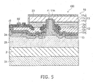
- FIG. 5 is a cross-sectional view taken along a line V-V of FIG. 4 .
- a semiconductor light-emitting element 100 includes a substrate 2, a structure body 10, a metal layer 24, an alloy layer 25, a back surface electrode 31, a p-pad electrode 32, and a protective layer 33.
- the back surface electrode 31 is disposed at a back surface of the semiconductor light-emitting element 100.
- the substrate 2 is disposed on the back surface electrode 31.
- the alloy layer 25 is disposed on the substrate 2. A portion of the alloy layer 25 protrudes upward at positions above which the recess r1 and the recess r2 of the structure body 10 are defined.
- the metal layer 24 and the electrode film 13 are disposed along corresponding surfaces of the alloy layer 25.
- the stacked body 12 is disposed on the electrode film 13 around the recess r1.
- the semiconductor stacked body 11 and the p-pad electrode 32 are disposed on the stacked body 12.
- the p-pad electrode 32 is spaced apart from the semiconductor stacked body 11 in a plan view.
- the semiconductor stacked body 11 includes an n-type semiconductor layer 11a, a p-type semiconductor layer 11b, and a light-emitting layer 11c.
- the stacked body 12 includes a p-side electrode 12a, an insulating layer 12b, an interconnect layer 12c, and an insulating layer 12d.
- the light-emitting layer 11c is disposed between the n-type semiconductor layer 11a and the p-type semiconductor layer 11b.
- the n-type semiconductor layer 11a is disposed at an upper surface side of the semiconductor light-emitting element 100 in the semiconductor stacked body 11.
- the p-type semiconductor layer 11b and the light-emitting layer 11c are disposed at a portion of the lower surface of the n-type semiconductor layer 11a overlapping a region where the recess r1 is not defined.
- the p-side electrode 12a is disposed under portions of the p-type semiconductor layer 11b around the recess r1.
- the insulating layer 12b covers the outer perimeter of the p-side electrode 12a and the lower surface of the p-type semiconductor layer 11b so that the interconnect layer 12c is prevented from being in contact with components other than the p-side electrode 12a.
- the interconnect layer 12c is disposed under the p-side electrode 12a and the insulating layer 12b and electrically connects the p-side electrode 12a and the p-pad electrode 32.
- the insulating layer 12d insulates the electrode film 13 from the interconnect layer 12c, the p-type semiconductor layer 11b, and the light-emitting layer 11c.
- the electrode film 13 is in contact with the n-type semiconductor layer 11a at the recess r1, and forms a contact surface 11n.
- the protective layer 33 covers corresponding surfaces of the semiconductor stacked body 11.
- the upper surface of the n-type semiconductor layer 11a may be a roughened surface that is configured to scatter light to improve the light extraction efficiency of the semiconductor light-emitting element 100.
- the semiconductor stacked body 11 contains gallium nitride.
- the p-side electrode 12a and the interconnect layer 12c contain a metal material such as aluminum, silver, indium, titanium, nickel, etc.
- the insulating layer 12b and the insulating layer 12d contain an insulating material such as silicon oxide, etc.
- the back surface electrode 31 at the back surface of the substrate 2 contains a metal such as platinum, etc.
- the p-pad electrode 32 contains a metal such as titanium, platinum, gold, etc.
- the protective layer 33 contains a transparent insulating material such as silicon oxide, etc.
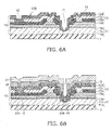
- FIG. 6A to FIG. 6F are schematic cross-sectional views of steps, showing an application example of the method of manufacturing the semiconductor element according to one embodiment of the invention.
- the structure body 10 is provided as shown in FIG. 6A .
- the structure body 10 includes the semiconductor stacked body 11 and the stacked body 12 described above.
- the surfaces 10S of the structure body 10 include surfaces defining the recess r1 and the recess r2 having a depth smaller than a depth of the recess r1.
- the metal layer 23a and the metal layer 23b are formed above at least a portion of the surfaces defining the recess r1 and at least a portion of the surfaces defining the recess r2 of the structure body 10, respectively.
- the metal layer 21 is formed at the surfaces 10S side of the structure body 10.
- the metal layer 21 is bonded to the metal layer 22 on the substrate 2 shown in FIG. 1E , so that the structure shown in FIG. 6C is obtained.
- the metal layer 21 and the metal layer 22 are bonded, and the metal layers 21, 22, 23a, 23b, and 24 are mixed to be alloyed, so that the alloy layer 25 is formed.
- the substrate 1 is removed as shown in FIG. 6D .
- the semiconductor stacked body 11 and the insulating layer 12b are processed, so that the p-pad electrode 32 and the protective layer 33 are formed.
- the back surface electrode 31 is formed at the backside of the substrate 2.
- the substrate 2 is diced at a dicing line DL shown in FIG. 6F .
- the dicing line DL is positioned in the region where the recess r2 is defined.
- the semiconductor light-emitting element 100 shown in FIG. 4 and FIG. 5 is manufactured through the steps described above.
Landscapes
- Led Devices (AREA)
- Electrodes Of Semiconductors (AREA)
Abstract
Description
- The present disclosure relates to a method of manufacturing a semiconductor element.
- Japanese Patent Publication No.
2016-174018 2016-174018 - A technique that allows for simplifying manufacturing steps and reducing manufacturing cost in a method of manufacturing a semiconductor element including such a bonding step would be desirable.
- The present disclosure includes the following inventions.
- (1) A method of manufacturing a semiconductor element, the method comprising: a first providing step comprising providing a structure body comprising a semiconductor stacked body, the structure body including first surfaces that include surfaces defining at least one first recess; a first forming step comprising forming a first rough-surface portion at or inward of at least a portion of the surfaces defining the first recess of the structure body, the first rough-surface portion being rougher than another portion of the first surfaces; a second forming step comprising forming a first metal layer at a first surface side of the structure body; a second providing step comprising providing a substrate on which a second metal layer is disposed; and a bonding step comprising heating the first metal layer and the second metal layer in a state in which the first metal layer and the second metal layer face each other such that the first metal layer and the second metal layer are melted and bonded together and the melted first metal layer flows into the first recess.
- (2) The method according to (1), wherein, in the bonding step, the first metal layer and the second metal layer are heated while pressing one of the structure body and the substrate toward the other of the structure body and the substrate.
- (3) The method according to (1) or (2), wherein, in the first forming step, a third metal layer is disposed along an inner surface of the first recess in at least a portion of the first recess to form the first rough-surface portion.
- (4) The method according to (3), wherein, in the first forming step, the third metal layer is formed using a plating technique.
- (5) The method according to (1) or (2), wherein: the first forming step comprises: forming a third metal layer along the first surface of the structure body; and forming the first rough-surface portion by roughening at least a portion of surfaces of the third metal layer in the first recess.
- (6) The method according to any one of (3) to (5), wherein a thickness of the third metal layer is less than a depth of the first recess.
- (7) The method according to any one of (3) to (6), further comprising: between the first providing step and the first forming step, a third forming step comprising forming a fourth metal layer at a first surface side of the structure body, wherein: the fourth metal layer contains nickel, the first metal layer contains tin, and the third metal layer contains nickel.
- (8) The method according to any one of (1) to (7), wherein: the first surfaces of the structure body include surfaces defining a second recess and surfaces defining a plurality of the first recesses, the second recess surrounding the plurality of first recesses and having a depth smaller than a depth of the first recesses, the first forming step further includes forming a second rough-surface portion at or inward of at least a portion of the surfaces defining the second recess, the second rough-surface portion being rougher than the other portion of the first surface, and in the bonding step, the first rough-surface portions cause the melted first metal layer to flow into the plurality of first recesses where the first rough-surface portions are formed and the second rough-surface portion causes the melted first metal layer to be flowed into the second recess where the second rough-surface portion is formed.
- (9) The method according to any one of (1) to (8), wherein: the semiconductor stacked body comprises an n-type semiconductor layer, a p-type semiconductor layer, and a light-emitting layer disposed between the n-type semiconductor layer and the p-type semiconductor layer, a portion of the n-type semiconductor layer is exposed at a bottom surface of the first recess of the structure body, and the first rough-surface portion formed in the first forming step is positioned at the exposed portion of the n-type semiconductor layer.
- The present disclosure allows for providing a method of manufacturing a semiconductor device in which steps can be simplified and manufacturing cost can be reduced.
-
-
FIG. 1A to FIG. 1H are schematic cross-sectional views illustrating steps in a method of manufacturing a semiconductor element according to one embodiment of the present invention; -
FIG. 2A, FIG. 2B ,FIG. 3A, and FIG. 3B are schematic cross-sectional views illustrating modified examples of the method of manufacturing the semiconductor element according to one embodiment of the present invention; -
FIG. 4 is a schematic plan view showing a semiconductor light-emitting element manufactured using the method of manufacturing the semiconductor element according to one embodiment of the present invention; -
FIG. 5 is a cross-sectional view taken along V-V line ofFIG. 4 ; and -
FIG. 6A to FIG. 6F are schematic cross-sectional views of steps, showing an application example of the method of manufacturing the semiconductor element according to one embodiment of the present invention. - Certain embodiments will be described with reference to the drawings. The same components in the drawings are designated with the same reference numerals.
-
FIG. 1A to FIG. 1H are schematic cross-sectional views illustrating steps in a method of manufacturing a semiconductor element according to one embodiment of the invention. - A
structure body 10 shown inFIG. 1A is provided (a first providing step). Thestructure body 10 is disposed on asubstrate 1, and includes a semiconductor stackedbody 11, a stackedbody 12, and anelectrode film 13. Thestructure body 10 includessurfaces 10S (i.e., first surfaces) that include surfaces defining a recess r1 (i.e., a first recess) and a recess r2 (i.e., a second recess). The recess r1 has a depth greater than a depth of the recess r2, extends through thestacked body 12, and reaches the semiconductor stackedbody 11. - The semiconductor stacked
body 11 is disposed on thesubstrate 1. Thesubstrate 1 is, for example, a sapphire substrate. The semiconductor stackedbody 11 includes a plurality of layers made of semiconductor materials such as silicon, gallium nitride, gallium arsenide, silicon nitride, etc. In the case of using a sapphire substrate for thesubstrate 1, it is preferable that the semiconductor stackedbody 11 includes a semiconductor material made of a nitride semiconductor such as InXAlYGa1-X-YN (0 ≤ X, 0 ≤ Y, and X + Y < 1), etc. The semiconductor stackedbody 11 may include semiconductor layers doped with impurities. - In a plan view, the stacked
body 12 is disposed on a surface of the semiconductor stackedbody 11 overlapping a region where the recess r1 is not provided. The stackedbody 12 includes, for example, one or more insulating layers and one or more metal layers. In one example, the insulating layer in the stackedbody 12 includes silicon nitride or silicon oxide. In one example, the metal layer in thestacked body 12 includes silver or aluminum. - The
electrode film 13 is disposed along thesurfaces 10S. In other words, theelectrode film 13 is located not only on the upper surface of thestacked body 12 but also on lateral surfaces and a bottom surface of the recess r1 and lateral surfaces and a bottom surface of the recess r2. Theelectrode film 13 may be a single layer or may have a layered structure. A portion of theelectrode film 13 on the bottom surface of the recess r1 is in contact with the semiconductor stackedbody 11. Theelectrode film 13 is provided to increase the electrical contact area between the semiconductor stackedbody 11 and another member bonded on theelectrode film 13. In one example, theelectrode film 13 includes aluminum or an alloy having aluminum as a main component. - Next, as shown in
FIG. 1B , in a third forming step, a metal layer 24 (i.e., a fourth metal layer) is formed along corresponding surfaces of theelectrode film 13. Themetal layer 24 functions as a seed layer when forming ametal layer 23a and ametal layer 23b described below using an electroplating technique. Themetal layer 24 may be a single layer or may have a stacked structure. For example, themetal layer 24 is formed by stacking a titanium layer, a nickel layer, and a gold layer, in this order, on a surface of theelectrode film 13. - Then, a rough-surface portion is formed at or inward of at least a portion of surfaces of the
structure body 10 that define the recess r1. The rough-surface portion in the recess r1 is referred to as a "first rough-surface portion". Also, another rough-surface portion is formed at or inward of at least a portion of surfaces defining the recess r2. The rough-surface portion in the recess r2 is referred to as a "second rough-surface portion". In the present embodiment, formation of the first rough-surface portion and second rough-surface portion are performed in a first forming step. For example, as shown inFIG. 1C , these rough-surface portions are formed by disposing ametal layer 23a (i.e., a third metal layer) and ametal layer 23b. Surfaces of themetal layer 23a opposite to themetal layer 24 and surfaces of themetal layer 23b opposite to themetal layer 24 are rough surfaces having an arithmetic average roughness Ra greater than the surfaces defining the recess r1 and the surfaces defining the recess r2 before forming themetal layer 23a and themetal layer 23b. With themetal layer 23a and themetal layer 23b, a roughness of at least a portion of the surfaces defining the recess r1 and a roughness of at least a portion of the surfaces defining the recess r2 are larger than a roughness of a surface of themetal layer 24. - For example, the
metal layer 23a and themetal layer 23b are formed using an electroplating technique. When forming themetal layer 23a and themetal layer 23b, a mask is formed on surfaces of thesurfaces 10S other than surfaces defining the recess r1 and the recess r2. A photoresist for a photolithography technique is used to form such a mask. Subsequently, electroplating is performed on thesurfaces 10S via the mask. Then, the mask is removed by etching, etc. Accordingly, themetal layer 23a and themetal layer 23b are formed on only at least a portion of the surfaces defining the recess r1 and at least a portion of the surfaces defining the recess r2, respectively. Thus, in this embodiment, the rough-surface portions are formed inward of at least a portion of the surfaces defining the first recess of the structure body. Any appropriate materials can be used for themetal layer 23a and themetal layer 23b. For example, themetal layer 23a and themetal layer 23b may be made of nickel. - A method other than plating may be used to form the
metal layer 23a and themetal layer 23b as long as these metal layers can be formed with roughened surface using the method. The formation of themetal layer 24 may be omitted when a technique other than a plating technique is used for forming of themetal layer 23a and themetal layer 23b. - Then, as shown in
FIG. 1D , in a second forming step, a metal layer 21 (i.e., a first metal layer) is formed on thestructure body 10 on which themetal layer 23a and themetal layer 23b are provided. For example, when forming themetal layer 21, themetal layer 21 is disposed along thesurfaces 10S, in the recess r1 and the recess r2. - The
metal layer 21 is disposed to bond thestructure body 10 to another member. Examples of a material of themetal layer 21 include any metal appropriate for bonding. For example, themetal layer 21 may be made of tin. - On the other hand, separately from the
structure body 10 as shown inFIG. 1E , asubstrate 2 on which a metal layer 22 (a second metal layer) is disposed is provided in a second providing step. For example, thesubstrate 2 made of Si, CuW, or the like. Themetal layer 22 is provided to be bonded to themetal layer 21 of thestructure body 10. Themetal layer 22 may be a single layer or may have a stacked structure. For example, themetal layer 22 is formed by stacking a platinum layer, a titanium layer, a nickel layer, and a tin layer, in this order. - Then, in a bonding step as shown in
FIG. 1F , themetal layer 21 and themetal layer 22 are caused to face each other, and themetal layer 21 and themetal layer 22 are bonded together. In the bonding step, heating is performed while pressing thesubstrate 1 and thesubstrate 2 toward each other. Accordingly, themetal layer 21 and themetal layer 22 are melted and are bonded together. Also, at this time, with the rough-surface portions inside the recess r1 and in the recess r2, the meltedmetal layer 21 and the meltedmetal layer 22 flow into the recess r1 and into the recess r2. Thus, the recess r1 and the recess r2 are filled with themetal layer 21, themetal layer 22, respectively, and the like. - By the bonding described above, for example, as shown in
FIG. 1G , corresponding ones of the metal layers 21, 22, 23a, 23b, and 24 are mixed and alloyed, so that analloy layer 25 is formed. After bonding, for example, as shown inFIG. 1H , thesubstrate 1 at thestructure body 10 side may be removed. - Effects obtained according to the first embodiment will be described with reference to comparative examples. Two methods described below are examples of methods of manufacturing according to the comparative examples.
- In a method according to Comparative Example 1, the
metal layer 21 is formed on thesurfaces 10S of thestructure body 10 defining the recess r1 without forming themetal layer 23a and themetal layer 23b. Subsequently, themetal layer 21 and themetal layer 22 formed on thesubstrate 2 are bonded together. - According to this method, the steps necessary for the bonding can be simplified. However, in this method, when a depth of the recess r1 is increased, the melted
metal layer 21 and the meltedmetal layer 22 do not flow sufficiently into the recess r1 in the bonding step. Accordingly, in the semiconductor element after bonding, a hollow (a void) is formed at the position where the recess r1 is provided. Presence of the hollow may cause reduction in the bonding strength, the electrical characteristics, and the heat dissipation of the semiconductor element. - In a method according to Comparative Example 2, a metal film with a high thickness for filling the recess is formed on the entirety of the
surfaces 10S of thestructure body 10 without forming themetal layer 23a and themetal layer 23b. Then, a surface of the metal film is planarized by etching. Next, themetal layer 21 is formed on the planarized surface of the metal film. Subsequently, themetal layer 21 and themetal layer 22 formed on thesubstrate 2 are bonded. - In the method according to Comparative Example 2, the recess of the
surfaces 10S is filled securely with the metal film, which allows for improving the bonding strength, the electrical characteristics, and the heat dissipation of the manufactured semiconductor element. On the other hand, the number of steps are increased in the method according to Comparative Example 2, which may increase the manufacturing cost. In particular, when the recess r1 has a high thickness, a metal film with a relatively high thickness needs to be formed to fill the recess r1. Therefore, a long period of time may be necessary to form and planarize the metal film, and the manufacturing cost may be further increased. - Compared to these methods, in the method of manufacturing according to the first embodiment, the
metal layer 23a that includes a rough-surface portion is formed at or inward of at least a portion of the surfaces defining the recess r1 instead of forming a metal film with a high thickness. The inventors have found that the rough-surface portion can facilitate flowing of the metal melted in the bonding step into the recess r1. With the rough-surface portion that can facilitate flowing of the melted metal into the recess r1, generation of a hollow at the portion where the recess r1 is provided in the semiconductor element after bonding can be prevented. - In other words, according to the method of manufacturing the semiconductor element according to the first embodiment, it is possible to fill the recess r1 with the
metal layer 21 and themetal layer 22 even without forming a metal film with a high thickness to fill the recess r1. Therefore, even when the metal film is not formed, the degradation of the electrical characteristics and decrease of heat dissipation can be reduced while ensuring the bonding strength of the manufactured semiconductor element. Also, formation of the metal film with a high thickness and planarization of the metal film are not required, which allows for simplifying the manufacturing steps, so that the manufacturing cost of the semiconductor element can be reduced. - As described above, according to the method of manufacturing the semiconductor element according to the first embodiment, it is possible to simplify the steps and reduce the manufacturing cost while reducing reduction of bonding strength, degradation of electrical characteristics, and reduction of heat dissipation.
- According to the method of manufacturing according to the first embodiment, a rough-surface portion (in the
metal layer 23b) is formed also at or inward of at least a portion of the surfaces defining the recess r2 even though the recess r2 is has a thickness smaller than a thickness of the recess r1. With this structure, in the semiconductor element after bonding, generation of a hollow at the position where the recess r2 is defined can be prevented, which allows for improving bonding strength, electrical characteristics, and heat dissipation. - Verifications by the inventors confirmed that the
metal layer 23a and themetal layer 23b each having surfaces with Ra of approximately 29.6 nm, and other surfaces with Ra of approximately 4.1 nm allows the meltedmetal layer 21 and the meltedmetal layer 22 to flow sufficiently into the recess r1 and the recess r2. - In the bonding step, it is desirable to heat the
metal layer 21 and themetal layer 22 while pressing one of the structure body 10 (more specifically, the substrate 1) and thesubstrate 2 toward the other of the structure body 10 (more specifically, the substrate 1) and thesubstrate 2. Pressing facilitates flowing of the meltedmetal layer 21 and the meltedmetal layer 22 into the recess r1 and the recess r2. Also, according to the first embodiment, the melted metals easily flow into the recess r1 and the recess r2, so that the load applied to thesubstrate 1 and thesubstrate 2 in bonding can be reduced. Therefore, damage of thesubstrate 1, thesubstrate 2, thestructure body 10, etc., in bonding can be suppressed, so that yield of the semiconductor element can be increased. - Any appropriate method can be used for forming the
metal layer 23a and themetal layer 23b as long as the surfaces of these metal layers can be roughened using the method. However, a plating technique is preferable for forming these metal layers. Using a plating technique allows for reducing a time for forming themetal layer 23a and themetal layer 23b that have rougher surfaces. - A thickness T1 of the
metal layer 23a and a thickness T2 of themetal layer 23b are desired to be relatively small. Reduction of the thickness T1 and the thickness T2 allows for reducing a time necessary to form themetal layer 23a and themetal layer 23b. According to the first embodiment, even if the thickness T1 and the thickness T2 are reduced, the rough-surface portions allows the meltedmetal layer 21 and the meltedmetal layer 22 to be sufficiently flowed into the recess r1 and into the recess r2. The thickness T1 of themetal layer 23a and the thickness T2 of themetal layer 23b are smaller than a depth D1 of the recess r1. It is preferable that the thickness T1 and the thickness T2 are smaller than a depth D2 and are 0.1 times to 0.5 times the depth D1, and are more preferably 0.15 times to 0.3 times the depth D1. With the thickness T1 and the thickness T2 that are 0.1 times the depth D1 or greater, the effect of rough-surface portions can be obtained effectively, so that the meltedmetal layer 21 and the meltedmetal layer 22 can be easily flowed into the recess r1 and r2. With the thickness T1 and the thickness T2 that are 0.5 times the depth D1 or smaller, the time for forming themetal layer 23a can be reduced, so that the yield can be increased. The depth D1 of the recess r1 can be, for example, approximately in a range of 4 µm to 7 µm. The depth D2 of the recess r2 can be, for example, approximately in a range of 1 µm to 3 µm. The thickness T1 and the thickness T2 can be, for example, approximately in a range of 1 µm to 3 µm. - Any appropriate materials may be used for the metal layers described above, it is desirable that the
metal layer 21 contains tin and themetal layer 22, themetal layer 23a, and themetal layer 23b contain nickel. Themetal layer 21 containing tin can have a lower melting point. Reduction in the melting point of themetal layer 21 allows reduction in the temperature when bonding thesubstrate 1 and thesubstrate 2 and reduction of damage to thestructure body 10 due to heat. Further, when themetal layer 22 contains nickel, an alloy of nickel of themetal layer 22 and tin of the meltedmetal layer 21 is formed. The melting point of an alloy of tin and nickel is higher than the melting point of simple tin. Accordingly, the heat resistance of the semiconductor element can be improved, and melting of the alloy layer in the steps after bonding can be prevented, so that the degree of freedom and the yield of the manufacturing steps of the semiconductor element can be increased. - In the bonding step, the alloy of tin and nickel described above may also be formed in the recess r1 and in the recess r2. The metal layers 23a and 23b in the recesses r1 and r2 allow a greater amount of tin to easily flow into the recesses r1 and r2, respectively. When a greater amount of tin is flowed into each of the recesses r1 and r2, a region far from the
second metal layer 22 and thefourth metal layer 24, which contain nickel, is more easily generated in each of the recesses r1 and r2 than in other alloyed portions. Nickel in thesecond metal layer 22 or thefourth metal layer 24 is not easily supplied to the region far from thesecond metal layer 22 and thefourth metal layer 24. However, with themetal layer 23a and themetal layer 23b containing nickel in the recess r1 and the recess r2, insufficiency of nickel can be compensated when forming the alloy in the recess r1 and the recess r2. Accordingly, the melting point of the alloy of tin and nickel in the recess r1 and the recess r2 can be more surely increased, so that the yield of the semiconductor element can be increased. -
FIG. 2A, FIG. 2B ,FIG. 3A, and FIG. 3B are schematic cross-sectional views of steps, showing modified examples of the method of manufacturing the semiconductor element according to the first embodiment of the present invention. - The
metal layer 23a and themetal layer 23b having rough surfaces are disposed to form rough-surface portions at or inward of at least a portion of the surfaces defining the recess r1 and the recess r2 in the example shown inFIG. 1A to FIG. 1H . Other methods may be employed for forming the rough-surface portions. - For example, in a modified example 1, after the
metal layer 24 is formed, ametal layer 23 is formed on an entirety of corresponding surfaces of themetal layer 24 as shown inFIG. 2A . Next, a surface of themetal layer 23 other than where the recess r1 and the recess r2 are defined is covered with a mask M1. Subsequently, as shown inFIG. 2B , at least a portion of surfaces of themetal layer 24 in the recess r1 and the recess r2 not covered with the mask M1 is processed, which roughens corresponding surfaces of themetal layer 24. Examples of more specific methods for processing corresponding surfaces of themetal layer 24 include exposing the surfaces not covered with the mask M1 to plasma of an active gas or an inert gas, irradiating the surfaces not covered with the mask M1 with an ion beam of an inert gas, and wet etching the surfaces not covered with the mask M1 using an etchant. - Alternatively, in a modified example 2, of the
surfaces 10S of thestructure body 10, surfaces other than surfaces defining the recess r1 and the recess r2 are covered with a mask M2 without forming themetal layer 24, as shown inFIG. 3A . Subsequently, as shown inFIG. 3B , of thesurfaces 10S of thestructure body 10, at least a portion of the surfaces defining the recess r1 and at least a portion of the surfaces defining the recess r2, which are not covered with the mask M2, are processed, which roughens corresponding surfaces. A method similar to the method described above is used to process thesurfaces 10S of thestructure body 10. - Using these methods also allows for forming rough-surface portions at at least a portion of the surfaces defining the recess r1 and inside the recess r2, as in the example shown in
FIG. 1A to FIG. 1H . In other words, using these methods also allows the meltedmetal layer 21 and the meltedmetal layer 22 to be easily flowed into the recess r1 and into the recess r2 in the bonding step. - The method of manufacturing the semiconductor element according to the first embodiment is widely applicable to bonding of two members in which a recess is defined in a surface of one of the members. In the description below, as an example, a case in which the method of manufacturing according to the first embodiment is applied to a method of manufacturing a semiconductor light-emitting element will be described.
- The structure of the semiconductor light-emitting element to be manufactured is described with reference to
FIG. 4 andFIG. 5 . -
FIG. 4 is a schematic plan view showing the semiconductor light-emitting element manufactured using the method of manufacturing the semiconductor element according to one embodiment of the invention. -
FIG. 5 is a cross-sectional view taken along a line V-V ofFIG. 4 . - As shown in
FIG. 4 andFIG. 5 , a semiconductor light-emittingelement 100 includes asubstrate 2, astructure body 10, ametal layer 24, analloy layer 25, aback surface electrode 31, a p-pad electrode 32, and aprotective layer 33. - The
back surface electrode 31 is disposed at a back surface of the semiconductor light-emittingelement 100. Thesubstrate 2 is disposed on theback surface electrode 31. Thealloy layer 25 is disposed on thesubstrate 2. A portion of thealloy layer 25 protrudes upward at positions above which the recess r1 and the recess r2 of thestructure body 10 are defined. Themetal layer 24 and theelectrode film 13 are disposed along corresponding surfaces of thealloy layer 25. - The
stacked body 12 is disposed on theelectrode film 13 around the recess r1. The semiconductor stackedbody 11 and the p-pad electrode 32 are disposed on thestacked body 12. The p-pad electrode 32 is spaced apart from the semiconductor stackedbody 11 in a plan view. - The semiconductor stacked
body 11 includes an n-type semiconductor layer 11a, a p-type semiconductor layer 11b, and a light-emittinglayer 11c. Thestacked body 12 includes a p-side electrode 12a, an insulatinglayer 12b, aninterconnect layer 12c, and an insulatinglayer 12d. - The light-emitting
layer 11c is disposed between the n-type semiconductor layer 11a and the p-type semiconductor layer 11b. - The n-
type semiconductor layer 11a is disposed at an upper surface side of the semiconductor light-emittingelement 100 in the semiconductor stackedbody 11. In a plan view, the p-type semiconductor layer 11b and the light-emittinglayer 11c are disposed at a portion of the lower surface of the n-type semiconductor layer 11a overlapping a region where the recess r1 is not defined. - The p-
side electrode 12a is disposed under portions of the p-type semiconductor layer 11b around the recess r1. The insulatinglayer 12b covers the outer perimeter of the p-side electrode 12a and the lower surface of the p-type semiconductor layer 11b so that theinterconnect layer 12c is prevented from being in contact with components other than the p-side electrode 12a. Theinterconnect layer 12c is disposed under the p-side electrode 12a and the insulatinglayer 12b and electrically connects the p-side electrode 12a and the p-pad electrode 32. The insulatinglayer 12d insulates theelectrode film 13 from theinterconnect layer 12c, the p-type semiconductor layer 11b, and the light-emittinglayer 11c. Theelectrode film 13 is in contact with the n-type semiconductor layer 11a at the recess r1, and forms acontact surface 11n. - The
protective layer 33 covers corresponding surfaces of the semiconductor stackedbody 11. The upper surface of the n-type semiconductor layer 11a may be a roughened surface that is configured to scatter light to improve the light extraction efficiency of the semiconductor light-emittingelement 100. - Examples of materials of the components will now be described.
- The semiconductor stacked
body 11 contains gallium nitride. The p-side electrode 12a and theinterconnect layer 12c contain a metal material such as aluminum, silver, indium, titanium, nickel, etc. The insulatinglayer 12b and the insulatinglayer 12d contain an insulating material such as silicon oxide, etc. - The
back surface electrode 31 at the back surface of thesubstrate 2 contains a metal such as platinum, etc. The p-pad electrode 32 contains a metal such as titanium, platinum, gold, etc. Theprotective layer 33 contains a transparent insulating material such as silicon oxide, etc. -
FIG. 6A to FIG. 6F are schematic cross-sectional views of steps, showing an application example of the method of manufacturing the semiconductor element according to one embodiment of the invention. - The
structure body 10 is provided as shown inFIG. 6A . Thestructure body 10 includes the semiconductor stackedbody 11 and thestacked body 12 described above. Thesurfaces 10S of thestructure body 10 include surfaces defining the recess r1 and the recess r2 having a depth smaller than a depth of the recess r1. - Next, the
metal layer 23a and themetal layer 23b are formed above at least a portion of the surfaces defining the recess r1 and at least a portion of the surfaces defining the recess r2 of thestructure body 10, respectively. Then, as shown inFIG. 6B , themetal layer 21 is formed at thesurfaces 10S side of thestructure body 10. Themetal layer 21 is bonded to themetal layer 22 on thesubstrate 2 shown inFIG. 1E , so that the structure shown inFIG. 6C is obtained. In other words, themetal layer 21 and themetal layer 22 are bonded, and the metal layers 21, 22, 23a, 23b, and 24 are mixed to be alloyed, so that thealloy layer 25 is formed. - Then, the
substrate 1 is removed as shown inFIG. 6D . Next, as shown inFIG. 6E , the semiconductor stackedbody 11 and the insulatinglayer 12b are processed, so that the p-pad electrode 32 and theprotective layer 33 are formed. Subsequently, as shown inFIG. 6F , theback surface electrode 31 is formed at the backside of thesubstrate 2. Then, thesubstrate 2 is diced at a dicing line DL shown inFIG. 6F . The dicing line DL is positioned in the region where the recess r2 is defined. The semiconductor light-emittingelement 100 shown inFIG. 4 andFIG. 5 is manufactured through the steps described above. - The embodiments described above are examples for giving a concrete form of the invention, and the scope of the present invention is not limited to the embodiments described above. Any appropriate modifications of the embodiments described above made by one skilled in the art without departing from the spirit of the present invention also are within the scope of the invention.
Claims (9)
- A method of manufacturing a semiconductor element, the method comprising:a first providing step comprising providing a structure body comprising a semiconductor stacked body, the structure body including first surfaces that include surfaces defining at least one first recess;a first forming step comprising forming a first rough-surface portion at or inward of at least a portion of the surfaces defining the first recess of the structure body, the first rough-surface portion being rougher than another portion of the first surfaces;a second forming step comprising forming a first metal layer at a first surface side of the structure body;a second providing step comprising providing a substrate on which a second metal layer is disposed; anda bonding step comprising heating the first metal layer and the second metal layer in a state in which the first metal layer and the second metal layer face each other such that the first metal layer and the second metal layer are melted and bonded together and the melted first metal layer flows into the first recess.
- The method according to claim 1, wherein, in the bonding step, the first metal layer and the second metal layer are heated while pressing one of the structure body and the substrate toward the other of the structure body and the substrate.
- The method according to claim 1 or 2, wherein, in the first forming step, a third metal layer is disposed along an inner surface of the first recess in at least a portion of the first recess to form the first rough-surface portion.
- The method according to claim 3, wherein, in the first forming step, the third metal layer is formed using a plating technique.
- The method according to claim 1 or 2, wherein:
the first forming step comprises:forming a third metal layer along the first surface of the structure body; andforming the first rough-surface portion by roughening at least a portion of surfaces of the third metal layer in the first recess. - The method according to claim 3 to 5, wherein a thickness of the third metal layer is less than a depth of the first recess.
- The method according to claim 3 to 6, further comprising:
between the first providing step and the first forming step, a third forming step comprising forming a fourth metal layer at a first surface side of the structure body, wherein:the fourth metal layer contains nickel,the first metal layer contains tin, andthe third metal layer contains nickel. - The method according to claim 1 to 7, wherein:the first surfaces of the structure body include surfaces defining a second recess and surfaces defining a plurality of the first recesses, the second recess surrounding the plurality of first recesses and having a depth smaller than a depth of the first recesses,the first forming step further includes forming a second rough-surface portion at or inward of at least a portion of the surfaces defining the second recess, the second rough-surface portion being rougher than the other portion of the first surface, andin the bonding step, the first rough-surface portions cause the melted first metal layer to flow into the plurality of first recesses where the first rough-surface portions are formed and the second rough-surface portion causes the melted first metal layer to be flowed into the second recess where the second rough-surface portion is formed.
- The method according to claim 1 to 8, wherein:the semiconductor stacked body comprises an n-type semiconductor layer, a p-type semiconductor layer, and a light-emitting layer disposed between the n-type semiconductor layer and the p-type semiconductor layer,a portion of the n-type semiconductor layer is exposed at a bottom surface of the first recess of the structure body, andthe first rough-surface portion formed in the first forming step is positioned at the exposed portion of the n-type semiconductor layer.
Applications Claiming Priority (1)
| Application Number | Priority Date | Filing Date | Title |
|---|---|---|---|
| JP2018176121A JP7096489B2 (en) | 2018-09-20 | 2018-09-20 | Manufacturing method of semiconductor device |
Publications (2)
| Publication Number | Publication Date |
|---|---|
| EP3627569A1 true EP3627569A1 (en) | 2020-03-25 |
| EP3627569B1 EP3627569B1 (en) | 2021-07-14 |
Family
ID=67998020
Family Applications (1)
| Application Number | Title | Priority Date | Filing Date |
|---|---|---|---|
| EP19198198.4A Active EP3627569B1 (en) | 2018-09-20 | 2019-09-19 | Method of manufacturing semiconductor element |
Country Status (4)
| Country | Link |
|---|---|
| US (1) | US10886428B2 (en) |
| EP (1) | EP3627569B1 (en) |
| JP (1) | JP7096489B2 (en) |
| KR (1) | KR102676518B1 (en) |
Citations (5)
| Publication number | Priority date | Publication date | Assignee | Title |
|---|---|---|---|---|
| US20060124954A1 (en) * | 2004-10-21 | 2006-06-15 | Nichia Corporation | Semiconductor light emitting device and method for manufacturing the same |
| JP2016174018A (en) | 2015-03-16 | 2016-09-29 | 株式会社東芝 | Semiconductor light emitting device |
| US20160365481A1 (en) * | 2015-06-15 | 2016-12-15 | Kabushiki Kaisha Toshiba | Semiconductor light-emitting device |
| US20170069792A1 (en) * | 2015-09-09 | 2017-03-09 | Kabushiki Kaisha Toshiba | Semiconductor light emitting device |
| US20180062025A1 (en) * | 2016-08-31 | 2018-03-01 | Nichia Corporation | Method for manufacturing light emitting element |
Family Cites Families (27)
| Publication number | Priority date | Publication date | Assignee | Title |
|---|---|---|---|---|
| WO2002027786A1 (en) * | 2000-09-25 | 2002-04-04 | Ibiden Co., Ltd. | Semiconductor element, method of manufacturing semiconductor element, multi-layer printed circuit board, and method of manufacturing multi-layer printed circuit board |
| JP4353167B2 (en) | 2004-10-21 | 2009-10-28 | 日亜化学工業株式会社 | Semiconductor light emitting device and manufacturing method thereof |
| JP5077068B2 (en) | 2007-05-30 | 2012-11-21 | 日亜化学工業株式会社 | Nitride semiconductor device and manufacturing method thereof |
| JP5123269B2 (en) * | 2008-09-30 | 2013-01-23 | ソウル オプト デバイス カンパニー リミテッド | Light emitting device and manufacturing method thereof |
| DE102009023849B4 (en) | 2009-06-04 | 2022-10-20 | OSRAM Opto Semiconductors Gesellschaft mit beschränkter Haftung | Optoelectronic semiconductor body and optoelectronic semiconductor chip |
| KR101106151B1 (en) * | 2009-12-31 | 2012-01-20 | 서울옵토디바이스주식회사 | Light emitting device and method of manufacturing the same |
| KR20120006410A (en) | 2010-07-12 | 2012-01-18 | 엘지이노텍 주식회사 | Light emitting device and manufacturing method |
| US8598614B2 (en) | 2010-08-30 | 2013-12-03 | Epistar Corporation | Light-emitting devices |
| TWI532214B (en) | 2010-10-12 | 2016-05-01 | Lg伊諾特股份有限公司 | Light-emitting element and its package |
| KR101115539B1 (en) * | 2011-06-10 | 2012-02-28 | 서울옵토디바이스주식회사 | Light emitting device and method of fabricating the same |
| JP6011108B2 (en) | 2011-09-27 | 2016-10-19 | 日亜化学工業株式会社 | Semiconductor element |
| KR101827975B1 (en) | 2011-10-10 | 2018-03-29 | 엘지이노텍 주식회사 | Light emitting device |
| US8581267B2 (en) | 2011-11-09 | 2013-11-12 | Toshiba Techno Center Inc. | Series connected segmented LED |
| JP5661660B2 (en) | 2012-02-07 | 2015-01-28 | 株式会社東芝 | Semiconductor light emitting device |
| KR102013363B1 (en) | 2012-11-09 | 2019-08-22 | 서울바이오시스 주식회사 | Light emitting device and method of fabricating the same |
| JP6024432B2 (en) | 2012-12-10 | 2016-11-16 | 日亜化学工業株式会社 | Semiconductor light emitting device |
| JP6287317B2 (en) | 2013-02-28 | 2018-03-07 | 日亜化学工業株式会社 | Semiconductor light emitting device |
| JP6221926B2 (en) | 2013-05-17 | 2017-11-01 | 日亜化学工業株式会社 | Semiconductor light emitting device and manufacturing method thereof |
| TWI591848B (en) | 2013-11-28 | 2017-07-11 | 晶元光電股份有限公司 | Light-emitting element and method of manufacturing same |
| JP2015173177A (en) | 2014-03-11 | 2015-10-01 | 株式会社東芝 | semiconductor light-emitting element |
| KR20160025456A (en) | 2014-08-27 | 2016-03-08 | 서울바이오시스 주식회사 | Light emitting diode and method of fabricating the same |
| JP2016134423A (en) | 2015-01-16 | 2016-07-25 | 株式会社東芝 | Semiconductor light emitting element, light emitting device and semiconductor light emitting element manufacturing method |
| JP6584799B2 (en) | 2015-03-16 | 2019-10-02 | アルパッド株式会社 | Semiconductor light emitting device |
| KR102378952B1 (en) | 2015-08-27 | 2022-03-25 | 쑤저우 레킨 세미컨덕터 컴퍼니 리미티드 | Light emitting device and light emitting device including the same |
| JP2017054963A (en) | 2015-09-10 | 2017-03-16 | 株式会社東芝 | Semiconductor light emitting device and manufacturing method thereof |
| JP2017162907A (en) | 2016-03-08 | 2017-09-14 | 株式会社東芝 | Bonding method and semiconductor device manufacturing method |
| TWI720053B (en) | 2016-11-09 | 2021-03-01 | 晶元光電股份有限公司 | Light-emitting element and manufacturing method thereof |
-
2018
- 2018-09-20 JP JP2018176121A patent/JP7096489B2/en active Active
-
2019
- 2019-09-19 EP EP19198198.4A patent/EP3627569B1/en active Active
- 2019-09-19 US US16/576,261 patent/US10886428B2/en active Active
- 2019-09-20 KR KR1020190115787A patent/KR102676518B1/en active Active
Patent Citations (5)
| Publication number | Priority date | Publication date | Assignee | Title |
|---|---|---|---|---|
| US20060124954A1 (en) * | 2004-10-21 | 2006-06-15 | Nichia Corporation | Semiconductor light emitting device and method for manufacturing the same |
| JP2016174018A (en) | 2015-03-16 | 2016-09-29 | 株式会社東芝 | Semiconductor light emitting device |
| US20160365481A1 (en) * | 2015-06-15 | 2016-12-15 | Kabushiki Kaisha Toshiba | Semiconductor light-emitting device |
| US20170069792A1 (en) * | 2015-09-09 | 2017-03-09 | Kabushiki Kaisha Toshiba | Semiconductor light emitting device |
| US20180062025A1 (en) * | 2016-08-31 | 2018-03-01 | Nichia Corporation | Method for manufacturing light emitting element |
Also Published As
| Publication number | Publication date |
|---|---|
| JP7096489B2 (en) | 2022-07-06 |
| KR20200033761A (en) | 2020-03-30 |
| US10886428B2 (en) | 2021-01-05 |
| US20200098946A1 (en) | 2020-03-26 |
| JP2020047835A (en) | 2020-03-26 |
| EP3627569B1 (en) | 2021-07-14 |
| KR102676518B1 (en) | 2024-06-18 |
Similar Documents
| Publication | Publication Date | Title |
|---|---|---|
| US20250056937A1 (en) | Etched trenches in bond materials for die singulation, and associated systems and methods | |
| US20150255685A1 (en) | Method for producing an optoelectronic component | |
| CN104167389B (en) | Semiconductor devices and its manufacture method with glass substrate | |
| KR102234785B1 (en) | Method for producing a plurality of optoelectronic semiconductor chips, and optoelectronic semiconductor chip | |
| US20080210955A1 (en) | Group III-V semiconductor device and method for producing the same | |
| US7642543B2 (en) | Semiconductor light emitting device having metal reflective layer | |
| US9147798B2 (en) | Semiconductor light emitting element and method for manufacturing same | |
| KR20110019416A (en) | Optoelectronic component and method for the production thereof | |
| US8232120B2 (en) | Manufacturing method of semiconductor light-emitting apparatus and semiconductor light-emitting apparatus | |
| JP2011223049A (en) | Method of removing substrate for high light extraction led | |
| KR20110082540A (en) | Method for manufacturing optoelectronic semiconductor device and optoelectronic semiconductor device | |
| WO2015077623A1 (en) | Led submount with integrated interconnects | |
| JP6367175B2 (en) | Semiconductor light emitting device | |
| JP2016174018A (en) | Semiconductor light emitting device | |
| JPS6159886A (en) | Manufacture of photosemiconductor device | |
| TW201532303A (en) | Method for stress-induced cutting semiconductor device | |
| EP3627569B1 (en) | Method of manufacturing semiconductor element | |
| US7541262B2 (en) | Method for producing semiconductor device | |
| JP5196288B2 (en) | Light emitting device manufacturing method and light emitting device | |
| TW200822389A (en) | Light emitting diode and method manufacturing the same | |
| WO2026094618A1 (en) | Method for manufacturing light-emitting element and light-emitting element | |
| JP2014506004A (en) | Method for manufacturing an electrical terminal support |
Legal Events
| Date | Code | Title | Description |
|---|---|---|---|
| PUAI | Public reference made under article 153(3) epc to a published international application that has entered the european phase |
Free format text: ORIGINAL CODE: 0009012 |
|
| STAA | Information on the status of an ep patent application or granted ep patent |
Free format text: STATUS: THE APPLICATION HAS BEEN PUBLISHED |
|
| AK | Designated contracting states |
Kind code of ref document: A1 Designated state(s): AL AT BE BG CH CY CZ DE DK EE ES FI FR GB GR HR HU IE IS IT LI LT LU LV MC MK MT NL NO PL PT RO RS SE SI SK SM TR |
|
| AX | Request for extension of the european patent |
Extension state: BA ME |
|
| STAA | Information on the status of an ep patent application or granted ep patent |
Free format text: STATUS: REQUEST FOR EXAMINATION WAS MADE |
|
| 17P | Request for examination filed |
Effective date: 20200925 |
|
| RBV | Designated contracting states (corrected) |
Designated state(s): AL AT BE BG CH CY CZ DE DK EE ES FI FR GB GR HR HU IE IS IT LI LT LU LV MC MK MT NL NO PL PT RO RS SE SI SK SM TR |
|
| GRAP | Despatch of communication of intention to grant a patent |
Free format text: ORIGINAL CODE: EPIDOSNIGR1 |
|
| STAA | Information on the status of an ep patent application or granted ep patent |
Free format text: STATUS: GRANT OF PATENT IS INTENDED |
|
| INTG | Intention to grant announced |
Effective date: 20210209 |
|
| GRAS | Grant fee paid |
Free format text: ORIGINAL CODE: EPIDOSNIGR3 |
|
| GRAA | (expected) grant |
Free format text: ORIGINAL CODE: 0009210 |
|
| STAA | Information on the status of an ep patent application or granted ep patent |
Free format text: STATUS: THE PATENT HAS BEEN GRANTED |
|
| AK | Designated contracting states |
Kind code of ref document: B1 Designated state(s): AL AT BE BG CH CY CZ DE DK EE ES FI FR GB GR HR HU IE IS IT LI LT LU LV MC MK MT NL NO PL PT RO RS SE SI SK SM TR |
|
| REG | Reference to a national code |
Ref country code: GB Ref legal event code: FG4D |
|
| REG | Reference to a national code |
Ref country code: DE Ref legal event code: R096 Ref document number: 602019006088 Country of ref document: DE |
|
| REG | Reference to a national code |
Ref country code: IE Ref legal event code: FG4D |
|
| REG | Reference to a national code |
Ref country code: AT Ref legal event code: REF Ref document number: 1411335 Country of ref document: AT Kind code of ref document: T Effective date: 20210815 |
|
| REG | Reference to a national code |
Ref country code: LT Ref legal event code: MG9D |
|
| REG | Reference to a national code |
Ref country code: NL Ref legal event code: MP Effective date: 20210714 |
|
| REG | Reference to a national code |
Ref country code: AT Ref legal event code: MK05 Ref document number: 1411335 Country of ref document: AT Kind code of ref document: T Effective date: 20210714 |
|
| PG25 | Lapsed in a contracting state [announced via postgrant information from national office to epo] |
Ref country code: FI Free format text: LAPSE BECAUSE OF FAILURE TO SUBMIT A TRANSLATION OF THE DESCRIPTION OR TO PAY THE FEE WITHIN THE PRESCRIBED TIME-LIMIT Effective date: 20210714 Ref country code: ES Free format text: LAPSE BECAUSE OF FAILURE TO SUBMIT A TRANSLATION OF THE DESCRIPTION OR TO PAY THE FEE WITHIN THE PRESCRIBED TIME-LIMIT Effective date: 20210714 Ref country code: RS Free format text: LAPSE BECAUSE OF FAILURE TO SUBMIT A TRANSLATION OF THE DESCRIPTION OR TO PAY THE FEE WITHIN THE PRESCRIBED TIME-LIMIT Effective date: 20210714 Ref country code: SE Free format text: LAPSE BECAUSE OF FAILURE TO SUBMIT A TRANSLATION OF THE DESCRIPTION OR TO PAY THE FEE WITHIN THE PRESCRIBED TIME-LIMIT Effective date: 20210714 Ref country code: LT Free format text: LAPSE BECAUSE OF FAILURE TO SUBMIT A TRANSLATION OF THE DESCRIPTION OR TO PAY THE FEE WITHIN THE PRESCRIBED TIME-LIMIT Effective date: 20210714 Ref country code: AT Free format text: LAPSE BECAUSE OF FAILURE TO SUBMIT A TRANSLATION OF THE DESCRIPTION OR TO PAY THE FEE WITHIN THE PRESCRIBED TIME-LIMIT Effective date: 20210714 Ref country code: BG Free format text: LAPSE BECAUSE OF FAILURE TO SUBMIT A TRANSLATION OF THE DESCRIPTION OR TO PAY THE FEE WITHIN THE PRESCRIBED TIME-LIMIT Effective date: 20211014 Ref country code: HR Free format text: LAPSE BECAUSE OF FAILURE TO SUBMIT A TRANSLATION OF THE DESCRIPTION OR TO PAY THE FEE WITHIN THE PRESCRIBED TIME-LIMIT Effective date: 20210714 Ref country code: NL Free format text: LAPSE BECAUSE OF FAILURE TO SUBMIT A TRANSLATION OF THE DESCRIPTION OR TO PAY THE FEE WITHIN THE PRESCRIBED TIME-LIMIT Effective date: 20210714 Ref country code: NO Free format text: LAPSE BECAUSE OF FAILURE TO SUBMIT A TRANSLATION OF THE DESCRIPTION OR TO PAY THE FEE WITHIN THE PRESCRIBED TIME-LIMIT Effective date: 20211014 Ref country code: PT Free format text: LAPSE BECAUSE OF FAILURE TO SUBMIT A TRANSLATION OF THE DESCRIPTION OR TO PAY THE FEE WITHIN THE PRESCRIBED TIME-LIMIT Effective date: 20211115 |
|
| PG25 | Lapsed in a contracting state [announced via postgrant information from national office to epo] |
Ref country code: PL Free format text: LAPSE BECAUSE OF FAILURE TO SUBMIT A TRANSLATION OF THE DESCRIPTION OR TO PAY THE FEE WITHIN THE PRESCRIBED TIME-LIMIT Effective date: 20210714 Ref country code: LV Free format text: LAPSE BECAUSE OF FAILURE TO SUBMIT A TRANSLATION OF THE DESCRIPTION OR TO PAY THE FEE WITHIN THE PRESCRIBED TIME-LIMIT Effective date: 20210714 Ref country code: GR Free format text: LAPSE BECAUSE OF FAILURE TO SUBMIT A TRANSLATION OF THE DESCRIPTION OR TO PAY THE FEE WITHIN THE PRESCRIBED TIME-LIMIT Effective date: 20211015 |
|
| REG | Reference to a national code |
Ref country code: DE Ref legal event code: R097 Ref document number: 602019006088 Country of ref document: DE |
|
| PG25 | Lapsed in a contracting state [announced via postgrant information from national office to epo] |
Ref country code: DK Free format text: LAPSE BECAUSE OF FAILURE TO SUBMIT A TRANSLATION OF THE DESCRIPTION OR TO PAY THE FEE WITHIN THE PRESCRIBED TIME-LIMIT Effective date: 20210714 |
|
| PLBE | No opposition filed within time limit |
Free format text: ORIGINAL CODE: 0009261 |
|
| REG | Reference to a national code |
Ref country code: BE Ref legal event code: MM Effective date: 20210930 |
|
| STAA | Information on the status of an ep patent application or granted ep patent |
Free format text: STATUS: NO OPPOSITION FILED WITHIN TIME LIMIT |
|
| PG25 | Lapsed in a contracting state [announced via postgrant information from national office to epo] |
Ref country code: SM Free format text: LAPSE BECAUSE OF FAILURE TO SUBMIT A TRANSLATION OF THE DESCRIPTION OR TO PAY THE FEE WITHIN THE PRESCRIBED TIME-LIMIT Effective date: 20210714 Ref country code: SK Free format text: LAPSE BECAUSE OF FAILURE TO SUBMIT A TRANSLATION OF THE DESCRIPTION OR TO PAY THE FEE WITHIN THE PRESCRIBED TIME-LIMIT Effective date: 20210714 Ref country code: RO Free format text: LAPSE BECAUSE OF FAILURE TO SUBMIT A TRANSLATION OF THE DESCRIPTION OR TO PAY THE FEE WITHIN THE PRESCRIBED TIME-LIMIT Effective date: 20210714 Ref country code: MC Free format text: LAPSE BECAUSE OF FAILURE TO SUBMIT A TRANSLATION OF THE DESCRIPTION OR TO PAY THE FEE WITHIN THE PRESCRIBED TIME-LIMIT Effective date: 20210714 Ref country code: EE Free format text: LAPSE BECAUSE OF FAILURE TO SUBMIT A TRANSLATION OF THE DESCRIPTION OR TO PAY THE FEE WITHIN THE PRESCRIBED TIME-LIMIT Effective date: 20210714 Ref country code: CZ Free format text: LAPSE BECAUSE OF FAILURE TO SUBMIT A TRANSLATION OF THE DESCRIPTION OR TO PAY THE FEE WITHIN THE PRESCRIBED TIME-LIMIT Effective date: 20210714 Ref country code: AL Free format text: LAPSE BECAUSE OF FAILURE TO SUBMIT A TRANSLATION OF THE DESCRIPTION OR TO PAY THE FEE WITHIN THE PRESCRIBED TIME-LIMIT Effective date: 20210714 |
|
| 26N | No opposition filed |
Effective date: 20220419 |
|
| PG25 | Lapsed in a contracting state [announced via postgrant information from national office to epo] |
Ref country code: LU Free format text: LAPSE BECAUSE OF NON-PAYMENT OF DUE FEES Effective date: 20210919 Ref country code: IT Free format text: LAPSE BECAUSE OF FAILURE TO SUBMIT A TRANSLATION OF THE DESCRIPTION OR TO PAY THE FEE WITHIN THE PRESCRIBED TIME-LIMIT Effective date: 20210714 Ref country code: IE Free format text: LAPSE BECAUSE OF NON-PAYMENT OF DUE FEES Effective date: 20210919 Ref country code: BE Free format text: LAPSE BECAUSE OF NON-PAYMENT OF DUE FEES Effective date: 20210930 |
|
| REG | Reference to a national code |
Ref country code: CH Ref legal event code: PL |
|
| P01 | Opt-out of the competence of the unified patent court (upc) registered |
Effective date: 20230522 |
|
| PG25 | Lapsed in a contracting state [announced via postgrant information from national office to epo] |
Ref country code: CY Free format text: LAPSE BECAUSE OF FAILURE TO SUBMIT A TRANSLATION OF THE DESCRIPTION OR TO PAY THE FEE WITHIN THE PRESCRIBED TIME-LIMIT Effective date: 20210714 |
|
| PG25 | Lapsed in a contracting state [announced via postgrant information from national office to epo] |
Ref country code: LI Free format text: LAPSE BECAUSE OF NON-PAYMENT OF DUE FEES Effective date: 20220930 Ref country code: HU Free format text: LAPSE BECAUSE OF FAILURE TO SUBMIT A TRANSLATION OF THE DESCRIPTION OR TO PAY THE FEE WITHIN THE PRESCRIBED TIME-LIMIT; INVALID AB INITIO Effective date: 20190919 Ref country code: CH Free format text: LAPSE BECAUSE OF NON-PAYMENT OF DUE FEES Effective date: 20220930 |
|
| PG25 | Lapsed in a contracting state [announced via postgrant information from national office to epo] |
Ref country code: MK Free format text: LAPSE BECAUSE OF FAILURE TO SUBMIT A TRANSLATION OF THE DESCRIPTION OR TO PAY THE FEE WITHIN THE PRESCRIBED TIME-LIMIT Effective date: 20210714 |
|
| PG25 | Lapsed in a contracting state [announced via postgrant information from national office to epo] |
Ref country code: TR Free format text: LAPSE BECAUSE OF FAILURE TO SUBMIT A TRANSLATION OF THE DESCRIPTION OR TO PAY THE FEE WITHIN THE PRESCRIBED TIME-LIMIT Effective date: 20210714 |
|
| PG25 | Lapsed in a contracting state [announced via postgrant information from national office to epo] |
Ref country code: MT Free format text: LAPSE BECAUSE OF FAILURE TO SUBMIT A TRANSLATION OF THE DESCRIPTION OR TO PAY THE FEE WITHIN THE PRESCRIBED TIME-LIMIT Effective date: 20210714 |
|
| REG | Reference to a national code |
Ref country code: DE Ref legal event code: R079 Ref document number: 602019006088 Country of ref document: DE Free format text: PREVIOUS MAIN CLASS: H01L0033000000 Ipc: H10H0020000000 |
|
| PGFP | Annual fee paid to national office [announced via postgrant information from national office to epo] |
Ref country code: DE Payment date: 20250730 Year of fee payment: 7 |
|
| PGFP | Annual fee paid to national office [announced via postgrant information from national office to epo] |
Ref country code: GB Payment date: 20250731 Year of fee payment: 7 |
|
| PGFP | Annual fee paid to national office [announced via postgrant information from national office to epo] |
Ref country code: FR Payment date: 20250808 Year of fee payment: 7 |