EP3627555A1 - Photodiode array - Google Patents
Photodiode array Download PDFInfo
- Publication number
- EP3627555A1 EP3627555A1 EP19201786.1A EP19201786A EP3627555A1 EP 3627555 A1 EP3627555 A1 EP 3627555A1 EP 19201786 A EP19201786 A EP 19201786A EP 3627555 A1 EP3627555 A1 EP 3627555A1
- Authority
- EP
- European Patent Office
- Prior art keywords
- semiconductor substrate
- surface side
- photodiode array
- multipliers
- accumulation
- Prior art date
- Legal status (The legal status is an assumption and is not a legal conclusion. Google has not performed a legal analysis and makes no representation as to the accuracy of the status listed.)
- Pending
Links
Images





Classifications
-
- H—ELECTRICITY
- H10—SEMICONDUCTOR DEVICES; ELECTRIC SOLID-STATE DEVICES NOT OTHERWISE PROVIDED FOR
- H10F—INORGANIC SEMICONDUCTOR DEVICES SENSITIVE TO INFRARED RADIATION, LIGHT, ELECTROMAGNETIC RADIATION OF SHORTER WAVELENGTH OR CORPUSCULAR RADIATION
- H10F39/00—Integrated devices, or assemblies of multiple devices, comprising at least one element covered by group H10F30/00, e.g. radiation detectors comprising photodiode arrays
- H10F39/10—Integrated devices
- H10F39/12—Image sensors
- H10F39/18—Complementary metal-oxide-semiconductor [CMOS] image sensors; Photodiode array image sensors
- H10F39/189—X-ray, gamma-ray or corpuscular radiation imagers
- H10F39/1898—Indirect radiation image sensors, e.g. using luminescent members
-
- H—ELECTRICITY
- H10—SEMICONDUCTOR DEVICES; ELECTRIC SOLID-STATE DEVICES NOT OTHERWISE PROVIDED FOR
- H10F—INORGANIC SEMICONDUCTOR DEVICES SENSITIVE TO INFRARED RADIATION, LIGHT, ELECTROMAGNETIC RADIATION OF SHORTER WAVELENGTH OR CORPUSCULAR RADIATION
- H10F30/00—Individual radiation-sensitive semiconductor devices in which radiation controls the flow of current through the devices, e.g. photodetectors
- H10F30/20—Individual radiation-sensitive semiconductor devices in which radiation controls the flow of current through the devices, e.g. photodetectors the devices having potential barriers, e.g. phototransistors
- H10F30/21—Individual radiation-sensitive semiconductor devices in which radiation controls the flow of current through the devices, e.g. photodetectors the devices having potential barriers, e.g. phototransistors the devices being sensitive to infrared, visible or ultraviolet radiation
- H10F30/22—Individual radiation-sensitive semiconductor devices in which radiation controls the flow of current through the devices, e.g. photodetectors the devices having potential barriers, e.g. phototransistors the devices being sensitive to infrared, visible or ultraviolet radiation the devices having only one potential barrier, e.g. photodiodes
- H10F30/225—Individual radiation-sensitive semiconductor devices in which radiation controls the flow of current through the devices, e.g. photodetectors the devices having potential barriers, e.g. phototransistors the devices being sensitive to infrared, visible or ultraviolet radiation the devices having only one potential barrier, e.g. photodiodes the potential barrier working in avalanche mode, e.g. avalanche photodiodes
-
- H—ELECTRICITY
- H10—SEMICONDUCTOR DEVICES; ELECTRIC SOLID-STATE DEVICES NOT OTHERWISE PROVIDED FOR
- H10F—INORGANIC SEMICONDUCTOR DEVICES SENSITIVE TO INFRARED RADIATION, LIGHT, ELECTROMAGNETIC RADIATION OF SHORTER WAVELENGTH OR CORPUSCULAR RADIATION
- H10F39/00—Integrated devices, or assemblies of multiple devices, comprising at least one element covered by group H10F30/00, e.g. radiation detectors comprising photodiode arrays
- H10F39/10—Integrated devices
- H10F39/107—Integrated devices having multiple elements covered by H10F30/00 in a repetitive configuration, e.g. radiation detectors comprising photodiode arrays
-
- H—ELECTRICITY
- H10—SEMICONDUCTOR DEVICES; ELECTRIC SOLID-STATE DEVICES NOT OTHERWISE PROVIDED FOR
- H10F—INORGANIC SEMICONDUCTOR DEVICES SENSITIVE TO INFRARED RADIATION, LIGHT, ELECTROMAGNETIC RADIATION OF SHORTER WAVELENGTH OR CORPUSCULAR RADIATION
- H10F39/00—Integrated devices, or assemblies of multiple devices, comprising at least one element covered by group H10F30/00, e.g. radiation detectors comprising photodiode arrays
- H10F39/80—Constructional details of image sensors
- H10F39/807—Pixel isolation structures
Definitions
- the present invention relates to a photodiode array to be used for photon counting by being operated in Geiger mode.
- a technique of photon counting by attaching a photodiode array using avalanche (electron avalanche) multiplication to a scintillator.
- avalanche electron avalanche
- a plurality of divided photodetecting channels are formed on a common substrate, and for each photodetecting channel, a multiplier is arranged (for example, refer to Non-patent Document 1 and Non-patent Document 2).
- Each multiplier is operated under operating conditions called Geiger mode in order to satisfactorily detect faint light. That is, a reverse voltage higher than a breakdown voltage is applied to each multiplier, and the phenomenon in which carriers generated due to photons that entered are avalanche-multiplied is used.
- a resistor for extracting an output signal from the multiplier is connected to each photodetecting channel, and the resistors are connected in parallel to each other. Photons that entered the photodetecting channels are detected based on a crest value of the output signal extracted to the outside via each resistor.
- the present invention was made in order to solve the problem, and an object thereof is to provide a photodiode array which can secure a sufficient aperture ratio with respect to light to be detected while restraining crosstalk between photodetecting channels even during operation in Geiger mode.
- a photodiode array relating to the present invention is a photodiode array obtained by forming, on a semiconductor substrate, a plurality of photodetecting channels which light to be detected is made to enter, and on an incident surface side which light to be detected enters of the semiconductor substrate, an accumulation layer having an impurity concentration higher than that of the semiconductor substrate is formed, and on a side opposite to the entrance surface of the semiconductor substrate, multipliers for avalanche-multiplying carriers generated due to incidence of light to be detected and resistors which are electrically connected to the multipliers and are connected in parallel to each other are formed for the respective photodetecting channels, and the photodetecting channels are separated from each other by separators formed around the respective multipliers.
- resistors to be electrically connected to the respective multipliers are collectively formed on the side opposite to the light-incident surface of the semiconductor substrate. Therefore, no resistor is interposed on the incident surface side which light to be detected enters, so that gaps between the photodetecting channels can be narrowed except for the forming regions of the separators. As a result, it becomes possible to secure a sufficient aperture ratio with respect to light to be detected while restraining crosstalk between photodetecting channels by the separators. Furthermore, on the incident surface side which light to be detected enters, an accumulation layer having an impurity concentration higher than that of the semiconductor substrate is formed, so that carriers generated in the semiconductor substrate can be restrained from being recombined near the incident surface side. Thereby, high quantum efficiency in each photodetecting channel is secured, so that improvement in effective aperture ratio with respect to light to be detected is realized.
- the separators are preferably formed by trenches. By employing trenches as separators, narrow separators can be formed, so that the aperture ratio with respect to light to be detected is more reliably secured.
- a low-refractive-index material having a refractive index lower than that of the semiconductor substrate is preferably formed.
- plasma emission generated in each multiplier under operating conditions of Geiger mode is reflected by the low-refractive-index material, and is restrained from reaching adjacent photodetecting channels.
- optical crosstalk can be restrained.
- the low-refractive-index material is preferably made of SiO 2 .
- a sufficient refractive index difference can be made between the low-refractive-index material and the semiconductor substrate. Therefore, plasma emission can be more reliably reflected by the low-refractive-index material, and optical crosstalk can be more effectively restrained.
- SiO 2 has high insulation, so that electrical crosstalk can also be effectively restrained.
- the trench and the low-refractive-index material are preferably formed so as to penetrate the semiconductor substrate from the incident surface side to the opposite surface side. Thereby, adjacent photodetecting channels are more reliably separated from each other, so that optical crosstalk and electrical crosstalk can be more effectively restrained.
- the accumulation layers are formed for the respective photodetecting channels, and the accumulation layers are electrically connected to each other by a transparent electrode layer formed on the incident surface side of the semiconductor substrate. Thereby, photodetecting channels are conducted to each other by the transparent electrode layer, and the same potential can be maintained. In this case, the accumulation layer lowers contact resistance between the semiconductor substrate and the transparent electrode layer, and a satisfactory contact can be formed.
- the photodiode array relating to the present invention even during operation in Geiger mode, a sufficient aperture ratio with respect to light to be detected can be secured while restraining crosstalk between photodetecting channels.
- Fig. 1 is a view of a photodiode array 1 of a first embodiment of the present invention from an incident surface side for light to be detected
- Fig. 2 is a view of the photodiode array 1 from an opposite side of the incident surface.
- the photodiode array 1 includes a semiconductor substrate 2, a transparent electrode layer 3, and pattern wirings 4.
- the semiconductor substrate 2 is in a square shape whose one side is about 1 to 5 mm, on which photodetecting channels 10 divided into a matrix (in this embodiment, 5 ⁇ 5) are formed.
- Each photodetecting channel 10 is in a square shape whose one side is about 5 to 100 ⁇ m, and the photodetecting channels are separated from each other by separators 5 formed like a lattice.
- separators 5 formed like a lattice.
- avalanche multipliers 6 in a predetermined pattern (rectangular pattern in this embodiment) for (electron) avalanche-multiplying carriers generated due to incidence of light to be detected are arranged, respectively.
- the transparent electrode layer 3 is made of, for example, ITO (Indium Tin Oxide), and is formed on the entire lower surface side (incident surface side for light to be detected) of the semiconductor substrate 2. This transparent electrode layer 3 allows transmission of light to be detected, and is electrically connected as an anode to each photodetecting channel 10.
- ITO Indium Tin Oxide
- the pattern wiring 4 includes an electrode 41 and a resistor 42 formed for each photodetecting channel 10, and a wiring 43, and is formed on the upper surface side (opposite surface side of the incident surface side) of the semiconductor substrate 2.
- the electrodes 41 are made of, for example, Al, and are electrically connected as cathodes to the respective photodetecting channels 10.
- the resistors 42 are made of, for example, polysilicon, and are electrically connected to the respective photodetecting channels 10 via the electrodes 41.
- the wiring 43 is made of, for example, Al, and connects the electrodes 41 and the resistors 42 in parallel, and its output side is connected to an amplifying circuit (not shown). With this construction, this photodiode array 1 is constructed as a so-called multichannel photodetecting element.
- Fig. 3 is a sectional view along the III-III line of Fig. 2 .
- each photodetecting channel 10 includes the above-described semiconductor substrate 2, the avalanche multiplier 6 formed on the upper surface side of the semiconductor substrate 2, and an accumulation layer 7 formed on the lower surface side.
- the photodetecting channels 10 adjacent to each other are separated from each other by a separator 5.
- the semiconductor substrate 2 is made of Si with a low impurity concentration whose conductivity type is p-type, and its thickness is set to 2 to 10 ⁇ m.
- the avalanche multiplier 6 includes a p-type semiconductor layer 61 made of Si whose conductivity type is p-type and an n + -type semiconductor layer 62 made of Si with a high impurity concentration whose conductivity is n-type.
- This p-type semiconductor layer 61 is formed into a rectangular shape (see Fig. 1 ) having a predetermined depth on the upper surface side of the semiconductor substrate 2, and has an impurity concentration higher than that of the semiconductor substrate 2.
- the n + -type semiconductor layer 62 is formed into a rectangular shape (see Fig.
- n + -type semiconductor layer 62 is electrically connected to the electrode 41 as a cathode of the pattern wiring 4.
- the accumulation layer 7 is made of Si which is higher in an impurity concentration than the semiconductor substrate 2 and whose conductivity type is p-type, and its thickness is set to 0.5 to 1.0 ⁇ m. This accumulation layer 7 is electrically connected to the transparent electrode layer 3 as an anode formed on the lower surface of the accumulation layer.
- the separator 5 includes a trench 51 and a low-refractive-index material 52 formed in this trench 51.
- the trenches 51 are formed like a lattice so as to completely surround each avalanche multiplier 6, and the groove width thereof is not more than 5 ⁇ m.
- the low-refractive-index material 52 is made of SiO 2 in detail, and is formed into a layer with a refractive index (about 1.46) lower than that of the semiconductor substrate 2 and high insulation. These trench 51 and low-refractive-index material 52 are formed so as to penetrate the semiconductor substrate 2 from the upper surface side to the lower surface side in the thickness direction, and thereby, the photodetecting channels 10 and 10 adjacent to each other are electrically and optically separated from each other.
- the photodiode array 1 thus constructed When the photodiode array 1 thus constructed is used for photo counting, it is operated under operating conditions called Geiger mode. During operation under this Geiger mode, a reverse voltage (for example, 40V or more) higher than the breakdown voltage is applied to each photodetecting channel 10 via the electrode 41 and the transparent electrode layer 3. In this state, when light to be detected enters each photodetecting channel 10 from the lower surface side, the light to be detected is absorbed in the semiconductor substrate 2 and generates carriers. The generated carriers move to the upper surface side while accelerating according to an electric field in the semiconductor substrate 2, and are multiplied to about 1 ⁇ 10 6 times by each avalanche multiplier 6. Then, the multiplied carriers are extracted to the outside via the resistor 42 and the wiring 43 and detected based on a crest value of an output signal thereof.
- a reverse voltage for example, 40V or more
- the resistors 42 and the wirings 43 to be electrically connected to the respective avalanche multipliers 6 are collectively formed on the upper surface side of the semiconductor substrate 2. Therefore, the lower surface side of the semiconductor substrate 2 which does not include interposition of the resistors 42 and the wirings 43 is set as the incident side of the light to be detected, whereby it becomes possible to narrow the gap between the photodetecting channels except for the forming region of the separator 5. As a result, in the photodiode array 1, a sufficient aperture ratio with respect to the light to be detected can be secured while crosstalk between the photodetecting channels 10 is restrained by the separator 5.
- the accumulation layer 7 having an impurity concentration higher than that of the semiconductor substrate 2 is formed for each photodetecting channel 10, so that carriers generated in the semiconductor substrate 2 due to incidence of the light to be detected can be restrained from being recombined near the lower surface of the semiconductor substrate 2. Thereby, high quantum efficiency in each photodetecting channel 10 is secured, so that the effective aperture ratio with respect to light to be detected is improved.
- the separator 5 which separates photodetecting channels 10 adjacent to each other includes the trench 51 and the low-refractive-index material 52 formed in this trench 51.
- this separator 5 it becomes possible to restrain electrical crosstalk caused by movement of carriers generated in the semiconductor substrate 2 due to incidence of light to be detected to the adjacent photodetecting channel 10.
- a reverse voltage higher than the breakdown voltage is applied to each avalanche multiplier 6, so that plasma emission may be generated when multiplying carriers, however, plasma emission generated at this time is reflected to the inside of the same photodetecting channel 10 due to a refractive index difference between the low-refractive-index material 52 and the semiconductor substrate 2.
- the plasma emission can be effectively restrained from reaching the adjacent photodetecting channel 10, and optical crosstalk can also be restrained.
- the width of the separator 5 can be formed to be not more than 5 ⁇ m, so that the gap between the photodetecting channels 10 is hardly expanded, and an aperture ratio with respect to light to be detected is secured.
- the above-described crosstalk restraining effect becomes more conspicuous. That is, SiO 2 has high insulation, so that electrical crosstalk is more effectively restrained.
- the refractive index of SiO 2 is about 1.46, and the refractive index of the semiconductor substrate 2 made of Si is about 3.5 to 5.0, so that a sufficient refractive index difference is secured between the lower-refractive-index material 52 and the semiconductor substrate 2. Therefore, plasma emission can be more reliably reflected by the low-refractive-index material 52, and optical crosstalk is more effectively restrained.
- the trench 51 and the low-refractive-index material 52 are formed so as to penetrate the semiconductor substrate 2 from the upper surface side to the lower surface side, so that the photodetecting channels 10 adjacent to each other are more reliably separated from each other. This is especially effective for blocking plasma emission radiating in all directions from the respective avalanche multipliers 6 during operation in Geiger mode, and optical crosstalk can be more reliably restrained.
- the accumulation layers 7 formed on the lower surface side of the semiconductor substrate 2 are electrically connected to each other by the transparent electrode layer 3.
- the photodetecting channels 10 are conducted to each other by the transparent electrode layer 3, and the same potential can be maintained.
- the accumulation layers 7 lower the contact resistance between the semiconductor substrate 2 and the transparent electrode layer 3 and make it possible to form a satisfactory contact.
- a SOI (Silicon on insulator) substrate whose conductivity type is p-type and which has an intermediate insulating layer 19 is prepared as the semiconductor substrate 2.
- the lattice-like trenches 51 are formed so as to reach the upper surface of the intermediate insulating layer 19 from the upper surface of the SOI substrate to form photodetecting channels 10 into a matrix.
- the low-refractive-index material 52 is embedded in the entire trenches 51 to form the separators 5.
- a p-type impurity such as B (boron) is doped and diffused from the upper surface side of the semiconductor substrate 2, and a p-type semiconductor layer 61 with a predetermined thickness is formed on the upper surface side of this semiconductor substrate 2. Furthermore, an n-type impurity such as P (phosphorus) is doped and diffused from the upper surface side of this p-type semiconductor layer 61, and on the upper surface side of the p-type semiconductor layer 61, an n + -type semiconductor layer 62 with a predetermined thickness is formed. Thereby, avalanche multipliers 6 are formed on the upper surface side of the semiconductor substrate 2. Then, as shown in Fig.
- an insulating layer 8 is formed on the upper surface of the semiconductor substrate 2 by using, for example, thermal oxidation.
- the process of forming the avalanche multipliers 6 may be performed prior to the process of forming the separators 5.
- the intermediate insulating layer 19 of the SOI substrate and the silicon layer on the lower surface side than the intermediate insulating layer 19 are removed by etching to expose the lower surface side of the semiconductor substrate 2.
- a p-type impurity such as B (boron) is doped and diffused from the lower surface side of the semiconductor substrate 2 to form an accumulation layer 7 for each photodetecting channel 10, and necessary portions of the insulating layer 8 are holed by using a photoresist, and then pattern wirings 4 are formed by sputtering or vapor deposition on the upper surface of the insulating layer 8.
- a transparent electrode layer 3 is formed last by, for example, vapor deposition on the lower surface sides of the accumulation layers 7 to electrically connect the accumulation layers 7 to each other, whereby the multichannel type photodiode array 1 shown in Fig. 1 through Fig. 3 is completed.
- the p-type semiconductor layer 61 in each avalanche multiplier 6 may be formed to have a thickness reaching the accumulation layer 7, and the resistor 42 may be formed so as to overlap the n + -type semiconductor layer 62 via the insulating layer 8.
- an accumulation layer 7A may be formed on the entire lower surface side of the semiconductor substrate 2.
- a guard ring made of a semiconductor layer whose conductivity type is n-type may be formed on the peripheral portion of each avalanche multiplier 6.
- the shapes of the trenches 51 shown have the same width from the upper surface side to the lower surface side of the semiconductor substrate 2, however, without limiting to this, they may be formed into a shape whose width becomes wider on the upper surface (n + -type semiconductor layer 62 surface) side than on the lower surface (light-incident surface) side, and vice versa.
- the photodiode array 20 of the second embodiment is different in that the n + -type semiconductor layer 62A forming each avalanche multiplier 6 is formed over the entire surface of each photodetecting channel 10 and is in contact with the surrounding separators 5 as shown in Fig. 8 .
- the resistors 42 and wirings 43 thereof to be electrically connected to the respective avalanche multipliers 6 are collectively formed on the upper surface side of the semiconductor substrate 2, so that by setting the lower surface side of the semiconductor substrate 2 as an incident side of light to be detected, the gaps between the photodetecting channels 10 can be narrowed except for the forming regions of the separators 5. As a result, a sufficient aperture ratio with respect to light to be detected can be secured while restraining crosstalk between the photodetecting channels 10 by the separators 5. Furthermore, on the lower surface side of the semiconductor substrate 2 as an incident side of light to be detected, the accumulation layers 7 are formed, so that high quantum efficiency in each photodetecting channel 10 is secured, and an effective aperture ratio with respect to light to be detected is improved.
- the accumulation layers 7 are electrically connected to each other by the transparent electrode layer 3. Thereby, the photodetecting channels 10 are conducted to each other, and the same potential can be maintained.
- the accumulation layers lower the contact resistance between the semiconductor substrate 2 and the transparent electrode layer 3 and make it possible to form a satisfactory contact.
- the separators 5 and photodetecting channels 10 are formed in the SOI substrate prepared as the semiconductor substrate 2.
- a p-type impurity such as B (boron) is doped and diffused from the upper surface side of the semiconductor substrate 2 to form p-type semiconductor layers 61 with a predetermined thickness on the upper surface side of the semiconductor substrate 2.
- an n-type impurity such as P (phosphorus) is doped and diffused for the entire surfaces of the photodetecting channels 10 from the upper surface side of the p-type semiconductor layers 61 to form n + -type semiconductor layers 62A with a predetermined thickness on the upper surface side of the p-type semiconductor layers 61.
- avalanche multipliers 6 are formed on the upper surface side of the semiconductor substrate 2.
- the process of forming the avalanche multipliers 6 may be performed prior to the process of forming the separators 5.
- an insulating layer 8 is formed on the upper surface of the semiconductor substrate 2 by using, for example, thermal oxidation as shown in Fig. 9-(b) .
- the intermediate insulating layer 19 of the SOI substrate and a silicon layer on the lower surface side than the intermediate insulating layer 19 are removed by etching to expose the lower surface side of the semiconductor substrate 2.
- a p-type impurity such as B (boron) is doped and diffused from this exposed lower surface side of the semiconductor substrate 2 to form an accumulation layer 7 for each photodetecting channel 10, and furthermore, necessary portions of the insulating layer 8 are holed by using a photoresist, and then pattern wirings 4 are formed by, for example, sputtering or vapor deposition.
- a transparent electrode layer 3 is formed last by, for example, vapor deposition on the lower surface sides of the accumulation layers 7 to electrically connect the accumulation layers 7 to each other, whereby the so-called multichannel type photodiode 20 shown in Fig. 8 is completed.
- the p-type semiconductor layers 61 may be formed so as to have a thickness reaching the accumulation layers 7, and the resistors 42 may be formed so as to overlap the n + semiconductor layers 62A via the insulating layer 8.
- an accumulation layer 7A formed on the entire lower surface side of the semiconductor substrate 2 may be employed as shown in Fig. 7 .
- the shapes of the trenches 51 shown have the same width from the upper surface side to the lower surface side of the semiconductor substrate 2, however, without limiting to this, they may be formed into a shape whose width becomes wider on the upper surface (n + -type semiconductor layer 62A surface) side than on the lower surface (light-incident surface) side, and vice versa.
- a photodiode array 22 according to a third embodiment is different in that both of the p-type semiconductor layers 61A and n + -type semiconductor layers 62A forming the avalanche multipliers 6 are formed over the entire surfaces of the photodetecting channels 10 and are in contact with the surrounding separators 5 as shown in Fig. 11 .
- the resistors 42 and wirings 43 thereof to be electrically connected to the respective avalanche multipliers 6 are collectively formed on the upper surface side of the semiconductor substrate 2, so that by setting the lower surface side of the semiconductor substrate 2 as an incident side of light to be detected, the gaps between the photodetecting channels 10 can be narrowed except for the forming regions of the separators 5. As a result, while restraining crosstalk between the photodetecting channels 10 by the separators 5, a sufficient aperture ratio with respect to light to be detected can be secured. Furthermore, on the lower surface side of the semiconductor substrate 2 as an incident side of light to be detected, accumulation layers 7 are formed, so that high quantum efficiency in each photodetecting channel 10 is secured, and an effective aperture ratio with respect to light to be detected is improved.
- the accumulation layers 7 are electrically connected to each other by the transparent electrode layer 3.
- the photodetecting channels 10 are conducted to each other by the transparent electrode layer 3, and the same potential can be maintained.
- the accumulation layers lower the contact resistance between the semiconductor substrate 2 and the transparent electrode layer 3 and make it possible to form a satisfactory contact.
- the separators 5 and the photodetectig channels 10 are formed in an SOI substrate prepared as the semiconductor substrate 2.
- a p-type impurity such as B (boron) is doped and diffused for the entire surface from the upper surface side of the semiconductor substrate 2 to form p-type semiconductor layers 61A with a predetermined thickness on the upper surface side of this semiconductor substrate 2.
- an n-type impurity such as P (phosphorus) is doped and diffused for the entire surfaces of the photodetecting channels 10 to form n + -type semiconductor layers 62A with a predetermined thickness on the upper surface sides of the p-type semiconductor layer 61A.
- avalanche multipliers 6 are formed on the upper surface side of the semiconductor substrate 2.
- the process of forming the avalanche multipliers 6 may be performed prior to the process of forming the separators 5.
- an insulating layer 8 is formed on the upper surface of the semiconductor substrate 2 by using, for example, thermal oxidation.
- the intermediate insulating layer 19 of the SOI substrate and the silicon layer on the lower surface side than the intermediate insulating layer 19 are removed by etching to expose the lower surface side of the semiconductor substrate 2.
- a p-type impurity such as B (boron) is doped and diffused from this exposed lower surface side of the semiconductor substrate 2 to form an accumulation layer 7 for each photodetecting channel 10, and furthermore, necessary portions of the insulating layer 8 are holed by using a photoresist, and then pattern wirings 4 are formed on the upper surface of the insulating layer 8 by, for example, sputtering or vapor deposition.
- a transparent electrode layer 3 is formed last on the lower surface sides of the accumulation layers 7 by, for example, vapor deposition to electrically connect the accumulation layers 7 to each other, whereby the so-called multichannel type photodiode array 22 shown in Fig. 11 is completed.
- the p-type semiconductor layers 61A may be formed so as to have a thickness reaching the accumulation layers 7, and the resistors 42 may be formed so as to overlap the n + semiconductor layers 62A via the insulating layer 8.
- an accumulation layer 7A may be formed on the entire lower surface side of the semiconductor substrate 2.
- the shapes of the trenches 51 shown have the same width from the upper surface side to the lower surface side of the semiconductor substrate 2, however, without limiting to this, they may be formed so as to have a width which becomes wider on the upper surface (n + -type semiconductor layer 62A surface) side than on the lower surface (light-incident surface) side, and vice versa.
- the present invention is usable for a photodiode array which is used for photon counting by being operated in Geiger mode.
Landscapes
- Light Receiving Elements (AREA)
- Solid State Image Pick-Up Elements (AREA)
Abstract
Description
- The present invention relates to a photodiode array to be used for photon counting by being operated in Geiger mode.
- For example, in chemical and medical fields, there is a technique of photon counting by attaching a photodiode array using avalanche (electron avalanche) multiplication to a scintillator. In such a photodiode array, in order to discriminate a plurality of photons which simultaneously enter, a plurality of divided photodetecting channels are formed on a common substrate, and for each photodetecting channel, a multiplier is arranged (for example, refer to Non-patent
Document 1 and Non-patent Document 2). - Each multiplier is operated under operating conditions called Geiger mode in order to satisfactorily detect faint light. That is, a reverse voltage higher than a breakdown voltage is applied to each multiplier, and the phenomenon in which carriers generated due to photons that entered are avalanche-multiplied is used. On the other hand, a resistor for extracting an output signal from the multiplier is connected to each photodetecting channel, and the resistors are connected in parallel to each other. Photons that entered the photodetecting channels are detected based on a crest value of the output signal extracted to the outside via each resistor.
- Non-patent Document 1: P. Buzhan, et al., "An Advanced Study of Silicon Photomultiplier" (online), ICFA Instrumentation BULLETIN Fall 2001 Issue, (searched on Nov. 4, 2004), (URL: http://www.slac.stanford.edu/pubs/icfa/)
- Non-patent Document 2: P. Buzhan, et al., "Silicon Photomultiplier And Its Possible Applications," Nuclear Instruments and Methods in Physics Research A 504(2003) 48-52
- When a photodiode array is used for photon counting, to obtain satisfactory results, it is important to increase quantum efficiency by raising the aperture ratio with respect to light to be detected and restrain crosstalk between photodetecting channels caused by operation in Geiger mode.
- However, in the above-described photodiode array, to restrain crosstalk between photodetecting channels caused during operation in Geiger mode, it is necessary to space the multipliers from each other to some degree. This results in lowering in aperture ratio with respect to light to be detected, and it is difficult to improve the detection sensitivity.
- The present invention was made in order to solve the problem, and an object thereof is to provide a photodiode array which can secure a sufficient aperture ratio with respect to light to be detected while restraining crosstalk between photodetecting channels even during operation in Geiger mode.
- To solve the problem, a photodiode array relating to the present invention is a photodiode array obtained by forming, on a semiconductor substrate, a plurality of photodetecting channels which light to be detected is made to enter, and on an incident surface side which light to be detected enters of the semiconductor substrate, an accumulation layer having an impurity concentration higher than that of the semiconductor substrate is formed, and on a side opposite to the entrance surface of the semiconductor substrate, multipliers for avalanche-multiplying carriers generated due to incidence of light to be detected and resistors which are electrically connected to the multipliers and are connected in parallel to each other are formed for the respective photodetecting channels, and the photodetecting channels are separated from each other by separators formed around the respective multipliers.
- In this photodiode array, resistors to be electrically connected to the respective multipliers are collectively formed on the side opposite to the light-incident surface of the semiconductor substrate. Therefore, no resistor is interposed on the incident surface side which light to be detected enters, so that gaps between the photodetecting channels can be narrowed except for the forming regions of the separators. As a result, it becomes possible to secure a sufficient aperture ratio with respect to light to be detected while restraining crosstalk between photodetecting channels by the separators. Furthermore, on the incident surface side which light to be detected enters, an accumulation layer having an impurity concentration higher than that of the semiconductor substrate is formed, so that carriers generated in the semiconductor substrate can be restrained from being recombined near the incident surface side. Thereby, high quantum efficiency in each photodetecting channel is secured, so that improvement in effective aperture ratio with respect to light to be detected is realized.
- The separators are preferably formed by trenches. By employing trenches as separators, narrow separators can be formed, so that the aperture ratio with respect to light to be detected is more reliably secured.
- In the trenches, a low-refractive-index material having a refractive index lower than that of the semiconductor substrate is preferably formed. Thereby, plasma emission generated in each multiplier under operating conditions of Geiger mode is reflected by the low-refractive-index material, and is restrained from reaching adjacent photodetecting channels. Thereby, optical crosstalk can be restrained.
- The low-refractive-index material is preferably made of SiO2. In this case, a sufficient refractive index difference can be made between the low-refractive-index material and the semiconductor substrate. Therefore, plasma emission can be more reliably reflected by the low-refractive-index material, and optical crosstalk can be more effectively restrained. Furthermore, SiO2 has high insulation, so that electrical crosstalk can also be effectively restrained.
- The trench and the low-refractive-index material are preferably formed so as to penetrate the semiconductor substrate from the incident surface side to the opposite surface side. Thereby, adjacent photodetecting channels are more reliably separated from each other, so that optical crosstalk and electrical crosstalk can be more effectively restrained.
- It is preferable that the accumulation layers are formed for the respective photodetecting channels, and the accumulation layers are electrically connected to each other by a transparent electrode layer formed on the incident surface side of the semiconductor substrate. Thereby, photodetecting channels are conducted to each other by the transparent electrode layer, and the same potential can be maintained. In this case, the accumulation layer lowers contact resistance between the semiconductor substrate and the transparent electrode layer, and a satisfactory contact can be formed.
- As described above, according to the photodiode array relating to the present invention, even during operation in Geiger mode, a sufficient aperture ratio with respect to light to be detected can be secured while restraining crosstalk between photodetecting channels.
- Further aspects of the present disclosure as set forth in the following numbered clauses:
-
Clause 1. A photodiode array having a plurality of photodetecting channels which is formed in a semiconductor substrate and light to be detected is made to enter, wherein:- on an incident surface side for the light to be detected of the semiconductor substrate,
- accumulation layers having an impurity concentration higher than in the semiconductor substrate are formed,
- on an opposite surface side of the incident surface of the semiconductor substrate,
- multipliers for avalanche-multiplying carriers generated due to incidence of the light to be detected; and
- resistors which are electrically connected to the multipliers and are connected in parallel to each other, are formed for the respective photodetecting channels, and
- the photodetecting channels are separated from each other by separators formed around the respective multipliers.
-
Clause 2. The photodiode array according toClause 1, wherein the separators are formed by trenches. -
Clause 3. The photodiode array according toClause 2, wherein in the trenches, a low-refractive index material having a refractive index lower than that of the semiconductor substrate is formed. -
Clause 4. The photodiode array according toClause 3, wherein the low-refractive index material is made of SiO2. -
Clause 5. The photodiode array according toClause 4, wherein the trench and the low-refractive-index material are formed so as to penetrate the semiconductor substrate from the incident surface side to the opposite surface side. -
Clause 6. The photodiode array according toClause 1, wherein
the accumulation layers are formed for the respective photodetecting channels, and
the accumulation layers are electrically connected to each other by a transparent electrode layer formed on the incident surface side of the semiconductor substrate. -
-
Fig. 1 is a view of a photodiode array of a first embodiment of the present invention from a light-incident surface side; -
Fig. 2 is a view of the photodiode array ofFig. 1 from an opposite side of the light-incident surface; -
Fig. 3 is a sectional view along the III-III line ofFig. 2 ; -
Fig. 4-(a) is a sectional view showing a manufacturing process of the photodiode array ofFig. 1 ,Fig. 4-(b) is a sectional view of a subsequent manufacturing process, andFig. 4-(c) is a further subsequent manufacturing process; -
Fig. 5-(a) is a sectional view showing a manufacturing process subsequent toFig. 4-(c) , andFig. 5-(b) is a sectional view showing a manufacturing process subsequent toFig. 5-(a) ; -
Fig. 6-(a) is a sectional view showing a manufacturing process subsequent toFig. 5-(b) , andFig. 6-(b) is a sectional view showing a manufacturing process subsequent toFig. 6-(a) ; -
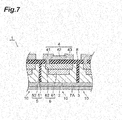
Fig. 7 is a sectional view showing an exemplary variation of the photodiode array of the first embodiment; -
Fig. 8 is a sectional view showing a photodiode array of a second embodiment of the present invention; -
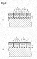
Fig. 9-(a) is a sectional view showing a manufacturing process of the photodiode array ofFig. 8 , andFig. 9-(b) is a sectional view showing a subsequent manufacturing process; -
Fig. 10(a) is a sectional view showing a manufacturing process subsequent toFig. 9-(b) , andFig. 10-(b) is a sectional view showing a manufacturing process subsequent toFig. 10-(a) ; -
Fig. 11 is a sectional view showing a photodiode array of a third embodiment of the present invention; -
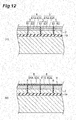
Fig. 12-(a) is a sectional view showing a manufacturing process of the photodiode array ofFig. 11 , andFig. 12-(b) is a sectional view of a subsequent manufacturing process; and -
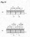
Fig. 13-(a) is a sectional view showing a manufacturing process subsequent toFig. 12-(b) , andFig. 13-(b) is a sectional view showing a manufacturing process subsequent toFig. 13-(a) . -
- 1: Photodiode array
- 2: Semiconductor substrate
- 3: Transparent electrode layer
- 5: Separator
- 6: Avalanche multiplier (multiplier)
- 7: Accumulation layer
- 10: Photodetecting channel
- 51: Trench
- 52: Low-refractive-index material
- 42: Resistor
- 20, 22: Photodiode array
- Hereinafter, preferred embodiments of the photodiode array relating to the present invention will be described in detail with reference to the drawings. The terms "upper," "lower," and the like are based on the state shown in the drawings, and are for descriptive purposes.
-
Fig. 1 is a view of aphotodiode array 1 of a first embodiment of the present invention from an incident surface side for light to be detected, andFig. 2 is a view of thephotodiode array 1 from an opposite side of the incident surface. - As shown in
Fig. 1 andFig. 2 , thephotodiode array 1 includes asemiconductor substrate 2, atransparent electrode layer 3, andpattern wirings 4. Thesemiconductor substrate 2 is in a square shape whose one side is about 1 to 5 mm, on whichphotodetecting channels 10 divided into a matrix (in this embodiment, 5×5) are formed. Eachphotodetecting channel 10 is in a square shape whose one side is about 5 to 100 µm, and the photodetecting channels are separated from each other byseparators 5 formed like a lattice. At central portions of therespective photodetecting channels 10,avalanche multipliers 6 in a predetermined pattern (rectangular pattern in this embodiment) for (electron) avalanche-multiplying carriers generated due to incidence of light to be detected are arranged, respectively. - The
transparent electrode layer 3 is made of, for example, ITO (Indium Tin Oxide), and is formed on the entire lower surface side (incident surface side for light to be detected) of thesemiconductor substrate 2. Thistransparent electrode layer 3 allows transmission of light to be detected, and is electrically connected as an anode to eachphotodetecting channel 10. - The
pattern wiring 4 includes anelectrode 41 and aresistor 42 formed for eachphotodetecting channel 10, and awiring 43, and is formed on the upper surface side (opposite surface side of the incident surface side) of thesemiconductor substrate 2. Theelectrodes 41 are made of, for example, Al, and are electrically connected as cathodes to therespective photodetecting channels 10. Theresistors 42 are made of, for example, polysilicon, and are electrically connected to therespective photodetecting channels 10 via theelectrodes 41. Thewiring 43 is made of, for example, Al, and connects theelectrodes 41 and theresistors 42 in parallel, and its output side is connected to an amplifying circuit (not shown). With this construction, thisphotodiode array 1 is constructed as a so-called multichannel photodetecting element. - Next, a detailed construction of each
photodetecting channel 10 will be described with reference toFig. 3. Fig. 3 is a sectional view along the III-III line ofFig. 2 . - As shown in
Fig. 3 , eachphotodetecting channel 10 includes the above-describedsemiconductor substrate 2, theavalanche multiplier 6 formed on the upper surface side of thesemiconductor substrate 2, and anaccumulation layer 7 formed on the lower surface side. Thephotodetecting channels 10 adjacent to each other are separated from each other by aseparator 5. - The
semiconductor substrate 2 is made of Si with a low impurity concentration whose conductivity type is p-type, and its thickness is set to 2 to 10 µm. Theavalanche multiplier 6 includes a p-type semiconductor layer 61 made of Si whose conductivity type is p-type and an n+-type semiconductor layer 62 made of Si with a high impurity concentration whose conductivity is n-type. This p-type semiconductor layer 61 is formed into a rectangular shape (seeFig. 1 ) having a predetermined depth on the upper surface side of thesemiconductor substrate 2, and has an impurity concentration higher than that of thesemiconductor substrate 2. The n+-type semiconductor layer 62 is formed into a rectangular shape (seeFig. 1 ) larger than (or equal in shape to) the p-type semiconductor layer 61, on the upper surface side of the p-type semiconductor layer 61, and p-n junction is formed between the same and the p-type semiconductor layer 61. An insulatinglayer 8 made of, for example, SiO2 is formed on the upper surface side of the n+-type semiconductor layer 62, and on this insulatinglayer 8, thepattern wiring 4 is formed. The n+-type semiconductor layer 62 is electrically connected to theelectrode 41 as a cathode of thepattern wiring 4. - The
accumulation layer 7 is made of Si which is higher in an impurity concentration than thesemiconductor substrate 2 and whose conductivity type is p-type, and its thickness is set to 0.5 to 1.0 µm. Thisaccumulation layer 7 is electrically connected to thetransparent electrode layer 3 as an anode formed on the lower surface of the accumulation layer. - The
separator 5 includes atrench 51 and a low-refractive-index material 52 formed in thistrench 51. Thetrenches 51 are formed like a lattice so as to completely surround eachavalanche multiplier 6, and the groove width thereof is not more than 5 µm. The low-refractive-index material 52 is made of SiO2 in detail, and is formed into a layer with a refractive index (about 1.46) lower than that of thesemiconductor substrate 2 and high insulation. Thesetrench 51 and low-refractive-index material 52 are formed so as to penetrate thesemiconductor substrate 2 from the upper surface side to the lower surface side in the thickness direction, and thereby, thephotodetecting channels - When the
photodiode array 1 thus constructed is used for photo counting, it is operated under operating conditions called Geiger mode. During operation under this Geiger mode, a reverse voltage (for example, 40V or more) higher than the breakdown voltage is applied to eachphotodetecting channel 10 via theelectrode 41 and thetransparent electrode layer 3. In this state, when light to be detected enters eachphotodetecting channel 10 from the lower surface side, the light to be detected is absorbed in thesemiconductor substrate 2 and generates carriers. The generated carriers move to the upper surface side while accelerating according to an electric field in thesemiconductor substrate 2, and are multiplied to about 1×10⁶ times by eachavalanche multiplier 6. Then, the multiplied carriers are extracted to the outside via theresistor 42 and thewiring 43 and detected based on a crest value of an output signal thereof. - As described above, in the
photodiode array 1 relating to this embodiment, theresistors 42 and thewirings 43 to be electrically connected to therespective avalanche multipliers 6 are collectively formed on the upper surface side of thesemiconductor substrate 2. Therefore, the lower surface side of thesemiconductor substrate 2 which does not include interposition of theresistors 42 and thewirings 43 is set as the incident side of the light to be detected, whereby it becomes possible to narrow the gap between the photodetecting channels except for the forming region of theseparator 5. As a result, in thephotodiode array 1, a sufficient aperture ratio with respect to the light to be detected can be secured while crosstalk between thephotodetecting channels 10 is restrained by theseparator 5. Furthermore, on the lower surface side of thesemiconductor substrate 2 as the incident surface side for light to be detected, theaccumulation layer 7 having an impurity concentration higher than that of thesemiconductor substrate 2 is formed for eachphotodetecting channel 10, so that carriers generated in thesemiconductor substrate 2 due to incidence of the light to be detected can be restrained from being recombined near the lower surface of thesemiconductor substrate 2. Thereby, high quantum efficiency in eachphotodetecting channel 10 is secured, so that the effective aperture ratio with respect to light to be detected is improved. - In the
photodiode array 1, theseparator 5 which separatesphotodetecting channels 10 adjacent to each other includes thetrench 51 and the low-refractive-index material 52 formed in thistrench 51. By thisseparator 5, it becomes possible to restrain electrical crosstalk caused by movement of carriers generated in thesemiconductor substrate 2 due to incidence of light to be detected to theadjacent photodetecting channel 10. Furthermore, during operation in Geiger mode of thephotodiode array 1, a reverse voltage higher than the breakdown voltage is applied to eachavalanche multiplier 6, so that plasma emission may be generated when multiplying carriers, however, plasma emission generated at this time is reflected to the inside of thesame photodetecting channel 10 due to a refractive index difference between the low-refractive-index material 52 and thesemiconductor substrate 2. Thereby, the plasma emission can be effectively restrained from reaching theadjacent photodetecting channel 10, and optical crosstalk can also be restrained. In addition, by employing thetrench 51 for forming theseparator 5, the width of theseparator 5 can be formed to be not more than 5 µm, so that the gap between thephotodetecting channels 10 is hardly expanded, and an aperture ratio with respect to light to be detected is secured. - By forming the low-refractive-
index material 52 from SiO2, the above-described crosstalk restraining effect becomes more conspicuous. That is, SiO2 has high insulation, so that electrical crosstalk is more effectively restrained. The refractive index of SiO2 is about 1.46, and the refractive index of thesemiconductor substrate 2 made of Si is about 3.5 to 5.0, so that a sufficient refractive index difference is secured between the lower-refractive-index material 52 and thesemiconductor substrate 2. Therefore, plasma emission can be more reliably reflected by the low-refractive-index material 52, and optical crosstalk is more effectively restrained. Furthermore, thetrench 51 and the low-refractive-index material 52 are formed so as to penetrate thesemiconductor substrate 2 from the upper surface side to the lower surface side, so that thephotodetecting channels 10 adjacent to each other are more reliably separated from each other. This is especially effective for blocking plasma emission radiating in all directions from therespective avalanche multipliers 6 during operation in Geiger mode, and optical crosstalk can be more reliably restrained. - Furthermore, in the
photodiode array 1, in therespective photodetecting channels 10, the accumulation layers 7 formed on the lower surface side of thesemiconductor substrate 2 are electrically connected to each other by thetransparent electrode layer 3. Thereby, thephotodetecting channels 10 are conducted to each other by thetransparent electrode layer 3, and the same potential can be maintained. The accumulation layers 7 lower the contact resistance between thesemiconductor substrate 2 and thetransparent electrode layer 3 and make it possible to form a satisfactory contact. - To manufacture the
photodiode array 1 having the above-described construction, first, as shown inFig. 4-(a) , a SOI (Silicon on insulator) substrate whose conductivity type is p-type and which has an intermediate insulatinglayer 19 is prepared as thesemiconductor substrate 2. Next, by etching using a predetermined mask (not shown), as shown inFig. 4-(b) , the lattice-like trenches 51 are formed so as to reach the upper surface of the intermediate insulatinglayer 19 from the upper surface of the SOI substrate to formphotodetecting channels 10 into a matrix. Furthermore, for example, by sputtering, as shown inFig. 4-(c) , the low-refractive-index material 52 is embedded in theentire trenches 51 to form theseparators 5. - Next, as shown in
Fig. 5-(a) , in eachphotodetecting channel 10, a p-type impurity such as B (boron) is doped and diffused from the upper surface side of thesemiconductor substrate 2, and a p-type semiconductor layer 61 with a predetermined thickness is formed on the upper surface side of thissemiconductor substrate 2. Furthermore, an n-type impurity such as P (phosphorus) is doped and diffused from the upper surface side of this p-type semiconductor layer 61, and on the upper surface side of the p-type semiconductor layer 61, an n+-type semiconductor layer 62 with a predetermined thickness is formed. Thereby,avalanche multipliers 6 are formed on the upper surface side of thesemiconductor substrate 2. Then, as shown inFig. 5-(b) , an insulatinglayer 8 is formed on the upper surface of thesemiconductor substrate 2 by using, for example, thermal oxidation. In this embodiment, the process of forming theavalanche multipliers 6 may be performed prior to the process of forming theseparators 5. - Furthermore, as shown in
Fig. 6-(a) , the intermediate insulatinglayer 19 of the SOI substrate and the silicon layer on the lower surface side than the intermediate insulatinglayer 19 are removed by etching to expose the lower surface side of thesemiconductor substrate 2. Next, as shown inFig. 6-(b) , a p-type impurity such as B (boron) is doped and diffused from the lower surface side of thesemiconductor substrate 2 to form anaccumulation layer 7 for eachphotodetecting channel 10, and necessary portions of the insulatinglayer 8 are holed by using a photoresist, and thenpattern wirings 4 are formed by sputtering or vapor deposition on the upper surface of the insulatinglayer 8. After forming the pattern wirings 4, atransparent electrode layer 3 is formed last by, for example, vapor deposition on the lower surface sides of the accumulation layers 7 to electrically connect the accumulation layers 7 to each other, whereby the multichanneltype photodiode array 1 shown inFig. 1 through Fig. 3 is completed. - Various variations may be applied to the layers of this embodiment. For example, the p-
type semiconductor layer 61 in eachavalanche multiplier 6 may be formed to have a thickness reaching theaccumulation layer 7, and theresistor 42 may be formed so as to overlap the n+-type semiconductor layer 62 via the insulatinglayer 8. Instead of forming theaccumulation layer 7 for eachphotodetecting channel 10, as shown inFig. 7 , anaccumulation layer 7A may be formed on the entire lower surface side of thesemiconductor substrate 2. Furthermore, on the peripheral portion of eachavalanche multiplier 6, a guard ring made of a semiconductor layer whose conductivity type is n-type may be formed. Thereby, theavalanche multiplier 6 can be protected from a leak of a high voltage by the guard ring, and uniform avalanche multiplication at the p-n junction is obtained. The shapes of thetrenches 51 shown have the same width from the upper surface side to the lower surface side of thesemiconductor substrate 2, however, without limiting to this, they may be formed into a shape whose width becomes wider on the upper surface (n+-type semiconductor layer 62 surface) side than on the lower surface (light-incident surface) side, and vice versa. - From the first embodiment having the n+-
type semiconductor layer 62 formed only at the center of eachphotodetecting channel 10, thephotodiode array 20 of the second embodiment is different in that the n+-type semiconductor layer 62A forming eachavalanche multiplier 6 is formed over the entire surface of eachphotodetecting channel 10 and is in contact with the surroundingseparators 5 as shown inFig. 8 . - Also in this
photodiode array 20, as in the first embodiment, theresistors 42 and wirings 43 thereof to be electrically connected to therespective avalanche multipliers 6 are collectively formed on the upper surface side of thesemiconductor substrate 2, so that by setting the lower surface side of thesemiconductor substrate 2 as an incident side of light to be detected, the gaps between thephotodetecting channels 10 can be narrowed except for the forming regions of theseparators 5. As a result, a sufficient aperture ratio with respect to light to be detected can be secured while restraining crosstalk between thephotodetecting channels 10 by theseparators 5. Furthermore, on the lower surface side of thesemiconductor substrate 2 as an incident side of light to be detected, the accumulation layers 7 are formed, so that high quantum efficiency in eachphotodetecting channel 10 is secured, and an effective aperture ratio with respect to light to be detected is improved. - Also in the
photodiode array 20, by theseparators 5 constructed in the same manner as in the first embodiment, electrical crosstalk and optical crosstalk can be effectively restrained. In addition, the employment oftrenches 51 for forming theseparators 5 hardly expand the gaps between thephotodetecting channels 10, and an aperture ratio with respect to light to be detected is secured. - Furthermore, also in the
photodiode array 20, the accumulation layers 7 are electrically connected to each other by thetransparent electrode layer 3. Thereby, thephotodetecting channels 10 are conducted to each other, and the same potential can be maintained. The accumulation layers lower the contact resistance between thesemiconductor substrate 2 and thetransparent electrode layer 3 and make it possible to form a satisfactory contact. - To manufacture such a
photodiode array 20, first, in the same manner as in the manufacturing processes shown inFig. 4-(a) through Fig. 4-(c) , theseparators 5 andphotodetecting channels 10 are formed in the SOI substrate prepared as thesemiconductor substrate 2. - Next, as shown in
Fig. 9-(a) , a p-type impurity such as B (boron) is doped and diffused from the upper surface side of thesemiconductor substrate 2 to form p-type semiconductor layers 61 with a predetermined thickness on the upper surface side of thesemiconductor substrate 2. Furthermore, an n-type impurity such as P (phosphorus) is doped and diffused for the entire surfaces of thephotodetecting channels 10 from the upper surface side of the p-type semiconductor layers 61 to form n+-type semiconductor layers 62A with a predetermined thickness on the upper surface side of the p-type semiconductor layers 61. Thereby,avalanche multipliers 6 are formed on the upper surface side of thesemiconductor substrate 2. In this embodiment, the process of forming theavalanche multipliers 6 may be performed prior to the process of forming theseparators 5. - Next, an insulating
layer 8 is formed on the upper surface of thesemiconductor substrate 2 by using, for example, thermal oxidation as shown inFig. 9-(b) . Then, as shown inFig. 10-(a) , the intermediate insulatinglayer 19 of the SOI substrate and a silicon layer on the lower surface side than the intermediate insulatinglayer 19 are removed by etching to expose the lower surface side of thesemiconductor substrate 2. Next, as shown inFig. 10-(b) , a p-type impurity such as B (boron) is doped and diffused from this exposed lower surface side of thesemiconductor substrate 2 to form anaccumulation layer 7 for eachphotodetecting channel 10, and furthermore, necessary portions of the insulatinglayer 8 are holed by using a photoresist, and thenpattern wirings 4 are formed by, for example, sputtering or vapor deposition. After forming the pattern wirings 4, atransparent electrode layer 3 is formed last by, for example, vapor deposition on the lower surface sides of the accumulation layers 7 to electrically connect the accumulation layers 7 to each other, whereby the so-calledmultichannel type photodiode 20 shown inFig. 8 is completed. - Various variations can also be applied to the layers of this embodiment. For example, the p-type semiconductor layers 61 may be formed so as to have a thickness reaching the accumulation layers 7, and the
resistors 42 may be formed so as to overlap the n+ semiconductor layers 62A via the insulatinglayer 8. Instead of the accumulation layers 7, anaccumulation layer 7A formed on the entire lower surface side of thesemiconductor substrate 2 may be employed as shown inFig. 7 . The shapes of thetrenches 51 shown have the same width from the upper surface side to the lower surface side of thesemiconductor substrate 2, however, without limiting to this, they may be formed into a shape whose width becomes wider on the upper surface (n+-type semiconductor layer 62A surface) side than on the lower surface (light-incident surface) side, and vice versa. - From the first embodiment having the p-type semiconductor layers 61 and the n+-type semiconductor layers 62 formed only at the centers of the
photodetecting channels 10, aphotodiode array 22 according to a third embodiment is different in that both of the p-type semiconductor layers 61A and n+-type semiconductor layers 62A forming theavalanche multipliers 6 are formed over the entire surfaces of thephotodetecting channels 10 and are in contact with the surroundingseparators 5 as shown inFig. 11 . - Also in this
photodiode array 22, as in the case of the first embodiment, theresistors 42 and wirings 43 thereof to be electrically connected to therespective avalanche multipliers 6 are collectively formed on the upper surface side of thesemiconductor substrate 2, so that by setting the lower surface side of thesemiconductor substrate 2 as an incident side of light to be detected, the gaps between thephotodetecting channels 10 can be narrowed except for the forming regions of theseparators 5. As a result, while restraining crosstalk between thephotodetecting channels 10 by theseparators 5, a sufficient aperture ratio with respect to light to be detected can be secured. Furthermore, on the lower surface side of thesemiconductor substrate 2 as an incident side of light to be detected, accumulation layers 7 are formed, so that high quantum efficiency in eachphotodetecting channel 10 is secured, and an effective aperture ratio with respect to light to be detected is improved. - Also in the
photodiode array 22, electrical crosstalk and optical crosstalk can be effectively restrained by theseparators 5 formed in the same manner as in the first embodiment. In addition, the employment oftrenches 51 for forming theseparators 5 hardly expands the gaps between thephotodetecting channels 10, and an aperture ratio with respect to light to be detected is secured. - Furthermore, also in the
photodiode array 22, the accumulation layers 7 are electrically connected to each other by thetransparent electrode layer 3. Thereby, thephotodetecting channels 10 are conducted to each other by thetransparent electrode layer 3, and the same potential can be maintained. The accumulation layers lower the contact resistance between thesemiconductor substrate 2 and thetransparent electrode layer 3 and make it possible to form a satisfactory contact. - To manufacture such a
photodiode array 22, first, in the same manner as in the manufacturing processes shown inFig. 4-(a) through Fig. 4-(c) , theseparators 5 and thephotodetectig channels 10 are formed in an SOI substrate prepared as thesemiconductor substrate 2. - Next, as shown in
Fig. 12-(a) , a p-type impurity such as B (boron) is doped and diffused for the entire surface from the upper surface side of thesemiconductor substrate 2 to form p-type semiconductor layers 61A with a predetermined thickness on the upper surface side of thissemiconductor substrate 2. Furthermore, from the upper surface sides of this p-type semiconductor layers 61A, an n-type impurity such as P (phosphorus) is doped and diffused for the entire surfaces of thephotodetecting channels 10 to form n+-type semiconductor layers 62A with a predetermined thickness on the upper surface sides of the p-type semiconductor layer 61A. Thereby, on the upper surface side of thesemiconductor substrate 2,avalanche multipliers 6 are formed. Also in this embodiment, the process of forming theavalanche multipliers 6 may be performed prior to the process of forming theseparators 5. - Next, as shown in
Fig. 12-(b) , an insulatinglayer 8 is formed on the upper surface of thesemiconductor substrate 2 by using, for example, thermal oxidation. As shown inFig. 13-(a) , the intermediate insulatinglayer 19 of the SOI substrate and the silicon layer on the lower surface side than the intermediate insulatinglayer 19 are removed by etching to expose the lower surface side of thesemiconductor substrate 2. Next, as shown inFig. 13-(b) a p-type impurity such as B (boron) is doped and diffused from this exposed lower surface side of thesemiconductor substrate 2 to form anaccumulation layer 7 for eachphotodetecting channel 10, and furthermore, necessary portions of the insulatinglayer 8 are holed by using a photoresist, and thenpattern wirings 4 are formed on the upper surface of the insulatinglayer 8 by, for example, sputtering or vapor deposition. After forming the pattern wirings 4, atransparent electrode layer 3 is formed last on the lower surface sides of the accumulation layers 7 by, for example, vapor deposition to electrically connect the accumulation layers 7 to each other, whereby the so-called multichanneltype photodiode array 22 shown inFig. 11 is completed. - Also to the layers of this embodiment, various variations can be applied. For example, the p-
type semiconductor layers 61A may be formed so as to have a thickness reaching the accumulation layers 7, and theresistors 42 may be formed so as to overlap the n+ semiconductor layers 62A via the insulatinglayer 8. Instead of the accumulation layers 7, as shown inFig. 7 , anaccumulation layer 7A may be formed on the entire lower surface side of thesemiconductor substrate 2. The shapes of thetrenches 51 shown have the same width from the upper surface side to the lower surface side of thesemiconductor substrate 2, however, without limiting to this, they may be formed so as to have a width which becomes wider on the upper surface (n+-type semiconductor layer 62A surface) side than on the lower surface (light-incident surface) side, and vice versa. - The present invention is usable for a photodiode array which is used for photon counting by being operated in Geiger mode.
Claims (8)
- A photodiode array (1, 20, 22) comprising:a plurality of photodetecting channels (10) which are formed in a semiconductor substrate (2) and light to be detected is made to enter;an accumulation layer (7A) or accumulation layers (7) having an impurity concentration higher than in the semiconductor substrate (2), the accumulation layer (7A) or the accumulation layers (7) formed at an incident surface side of the semiconductor substrate (2), the accumulation layers (7) being electrically connected to each other;PN junctions of multipliers formed at an opposite surface side of the incident surface of the semiconductor substrate (2), each of the multipliers avalanche-multiplying carriers;resistors (42), each formed on the opposite surface side of the incident surface and electrically connected to the multipliers; andseparators (5) formed around and separating the photodetecting channels (10),the accumulation layers (7), the multipliers (6) and the resistors (42) being respectively formed for each of the respective photodetecting channels (10), or the accumulation layer (7A) being formed over an entire surface of the incident surface side of the semiconductor substrate (2) while the multipliers (6) and the resistors (42) being respectively formed for each of the respective photodetecting channels (10).
- The photodiode array (1, 20, 22) according to claim 1, wherein the separators (5) are formed by trenches.
- The photodiode array (1, 20, 22) according to claim 2, wherein in the trenches, a low-refractive-index material having a refractive index lower than that of the semiconductor substrate (2) is formed.
- The photodiode array (1, 20, 22) according to claim 3, wherein the low-refractive-index material is made of SiO2.
- The photodiode array according to claim 4, wherein the trench (5) and the low-refractive-index material are formed so as to penetrate the semiconductor substrate (2) from the incident surface side to the opposite surface side.
- The photodiode array according to any one of claims 1 to 5, wherein the conductivity type of the accumulation layer (7A) or the accumulation layers (7) is the same as the conductivity type of the semiconductor substrate (2).
- The photodiode array according to any one of claims 1 to 6, wherein the resistors (42) are connected in parallel.
- The photodiode array according to any one of claims 1 to 7, wherein the separators (5) are formed around and separating the multipliers.
Applications Claiming Priority (3)
| Application Number | Priority Date | Filing Date | Title |
|---|---|---|---|
| JP2004374062A JP4841834B2 (en) | 2004-12-24 | 2004-12-24 | Photodiode array |
| PCT/JP2005/023503 WO2006068184A1 (en) | 2004-12-24 | 2005-12-21 | Photodiode array |
| EP05820225.0A EP1840967B1 (en) | 2004-12-24 | 2005-12-21 | Photodiode array |
Related Parent Applications (2)
| Application Number | Title | Priority Date | Filing Date |
|---|---|---|---|
| EP05820225.0A Division EP1840967B1 (en) | 2004-12-24 | 2005-12-21 | Photodiode array |
| EP05820225.0A Division-Into EP1840967B1 (en) | 2004-12-24 | 2005-12-21 | Photodiode array |
Publications (1)
| Publication Number | Publication Date |
|---|---|
| EP3627555A1 true EP3627555A1 (en) | 2020-03-25 |
Family
ID=36601781
Family Applications (2)
| Application Number | Title | Priority Date | Filing Date |
|---|---|---|---|
| EP05820225.0A Expired - Lifetime EP1840967B1 (en) | 2004-12-24 | 2005-12-21 | Photodiode array |
| EP19201786.1A Pending EP3627555A1 (en) | 2004-12-24 | 2005-12-21 | Photodiode array |
Family Applications Before (1)
| Application Number | Title | Priority Date | Filing Date |
|---|---|---|---|
| EP05820225.0A Expired - Lifetime EP1840967B1 (en) | 2004-12-24 | 2005-12-21 | Photodiode array |
Country Status (4)
| Country | Link |
|---|---|
| US (1) | US20090121306A1 (en) |
| EP (2) | EP1840967B1 (en) |
| JP (1) | JP4841834B2 (en) |
| WO (1) | WO2006068184A1 (en) |
Families Citing this family (63)
| Publication number | Priority date | Publication date | Assignee | Title |
|---|---|---|---|---|
| RU2290721C2 (en) | 2004-05-05 | 2006-12-27 | Борис Анатольевич Долгошеин | Silicon photoelectronic multiplier (alternatives) and locations for silicon photoelectronic multiplier |
| US8139130B2 (en) | 2005-07-28 | 2012-03-20 | Omnivision Technologies, Inc. | Image sensor with improved light sensitivity |
| US8274715B2 (en) | 2005-07-28 | 2012-09-25 | Omnivision Technologies, Inc. | Processing color and panchromatic pixels |
| US7916362B2 (en) | 2006-05-22 | 2011-03-29 | Eastman Kodak Company | Image sensor with improved light sensitivity |
| EP3002794B1 (en) | 2006-07-03 | 2020-08-19 | Hamamatsu Photonics K.K. | Photodiode array |
| US8188563B2 (en) * | 2006-07-21 | 2012-05-29 | The Regents Of The University Of California | Shallow-trench-isolation (STI)-bounded single-photon CMOS photodetector |
| US8031258B2 (en) | 2006-10-04 | 2011-10-04 | Omnivision Technologies, Inc. | Providing multiple video signals from single sensor |
| JP2008103614A (en) * | 2006-10-20 | 2008-05-01 | Mitsui Eng & Shipbuild Co Ltd | Photoelectric conversion device |
| US7652257B2 (en) * | 2007-06-15 | 2010-01-26 | General Electric Company | Structure of a solid state photomultiplier |
| US8896712B2 (en) | 2007-07-20 | 2014-11-25 | Omnivision Technologies, Inc. | Determining and correcting for imaging device motion during an exposure |
| DE102007037020B3 (en) * | 2007-08-06 | 2008-08-21 | MAX-PLANCK-Gesellschaft zur Förderung der Wissenschaften e.V. | Avalanche photodiode for use in Avalanche radiation detector, has electrode arranged lateral to diode layer so that it depletes substrate laterally adjacent to layer, when resistance layer is shielded from diode layer opposite to electrode |
| US8350952B2 (en) * | 2008-06-04 | 2013-01-08 | Omnivision Technologies, Inc. | Image sensors with improved angle response |
| US7915067B2 (en) * | 2008-07-09 | 2011-03-29 | Eastman Kodak Company | Backside illuminated image sensor with reduced dark current |
| US20100006908A1 (en) | 2008-07-09 | 2010-01-14 | Brady Frederick T | Backside illuminated image sensor with shallow backside trench for photodiode isolation |
| US7859033B2 (en) | 2008-07-09 | 2010-12-28 | Eastman Kodak Company | Wafer level processing for backside illuminated sensors |
| JP5185208B2 (en) * | 2009-02-24 | 2013-04-17 | 浜松ホトニクス株式会社 | Photodiode and photodiode array |
| JP5185206B2 (en) | 2009-02-24 | 2013-04-17 | 浜松ホトニクス株式会社 | Semiconductor photo detector |
| JP5805680B2 (en) * | 2009-02-24 | 2015-11-04 | 浜松ホトニクス株式会社 | Photodiode and photodiode array |
| JP5185207B2 (en) * | 2009-02-24 | 2013-04-17 | 浜松ホトニクス株式会社 | Photodiode array |
| JP5185205B2 (en) | 2009-02-24 | 2013-04-17 | 浜松ホトニクス株式会社 | Semiconductor photo detector |
| US8237831B2 (en) * | 2009-05-28 | 2012-08-07 | Omnivision Technologies, Inc. | Four-channel color filter array interpolation |
| JP2010283223A (en) * | 2009-06-05 | 2010-12-16 | Hamamatsu Photonics Kk | Semiconductor light detection element and method for manufacturing semiconductor light detection element |
| ITVI20100110A1 (en) * | 2010-04-22 | 2011-10-23 | Fond Bruno Kessler | PHOTOMOLTIPLICATOR DEVICE WITH A PERFECT SOLID STATE |
| JP5562207B2 (en) | 2010-10-29 | 2014-07-30 | 浜松ホトニクス株式会社 | Photodiode array |
| EP2549536B1 (en) * | 2011-07-22 | 2020-08-19 | Espros Photonics AG | Semiconductor structure for photon detection |
| US8941204B2 (en) * | 2012-04-27 | 2015-01-27 | Taiwan Semiconductor Manufacturing Company, Ltd. | Apparatus and method for reducing cross talk in image sensors |
| JP5984617B2 (en) | 2012-10-18 | 2016-09-06 | 浜松ホトニクス株式会社 | Photodiode array |
| US9160949B2 (en) * | 2013-04-01 | 2015-10-13 | Omnivision Technologies, Inc. | Enhanced photon detection device with biased deep trench isolation |
| GB201311055D0 (en) | 2013-06-21 | 2013-08-07 | St Microelectronics Res & Dev | Single-photon avalanche diode and an array thereof |
| JP2015056622A (en) * | 2013-09-13 | 2015-03-23 | 株式会社リコー | Semiconductor device |
| CN104752340B (en) * | 2013-12-31 | 2018-05-01 | 上海丽恒光微电子科技有限公司 | Avalanche photodiode array device and forming method, laser three-dimensional imaging device |
| JP2016092178A (en) * | 2014-11-04 | 2016-05-23 | 株式会社リコー | Solid state imaging device |
| CN105842706B (en) * | 2015-01-14 | 2019-02-22 | 上海丽恒光微电子科技有限公司 | Laser three-dimensional imaging device and manufacturing method thereof |
| US9450007B1 (en) | 2015-05-28 | 2016-09-20 | Stmicroelectronics S.R.L. | Integrated circuit with reflective material in trenches and related methods |
| JP6738129B2 (en) * | 2015-07-28 | 2020-08-12 | 株式会社東芝 | Photodetector and lidar device using the same |
| CN107949913B (en) * | 2015-09-09 | 2019-04-19 | 松下知识产权经营株式会社 | Solid-state imaging element |
| KR101762431B1 (en) * | 2015-12-22 | 2017-07-28 | 한국과학기술원 | Silicon photomultiplier having ree crosstalk structure |
| EP3309847B1 (en) | 2016-10-13 | 2024-06-05 | Canon Kabushiki Kaisha | Photo-detection apparatus and photo-detection system |
| JP6701135B2 (en) | 2016-10-13 | 2020-05-27 | キヤノン株式会社 | Photodetector and photodetection system |
| JP6712215B2 (en) * | 2016-11-11 | 2020-06-17 | 浜松ホトニクス株式会社 | Photo detector |
| EP3564711A4 (en) | 2016-12-27 | 2020-07-15 | Shimadzu Corporation | Photodetector |
| JP2018148183A (en) * | 2017-03-09 | 2018-09-20 | 株式会社東芝 | Optical detector and radiation detector |
| JP6884948B2 (en) * | 2017-03-17 | 2021-06-09 | 国立研究開発法人情報通信研究機構 | High speed photo detector array |
| KR20230170996A (en) * | 2017-11-15 | 2023-12-19 | 소니 세미컨덕터 솔루션즈 가부시키가이샤 | Light detecting element and method of manufacturing same |
| JP2018078304A (en) * | 2017-12-07 | 2018-05-17 | 株式会社東芝 | Photo-detector |
| JP6874714B2 (en) | 2018-02-22 | 2021-05-19 | 株式会社豊田中央研究所 | Photodetector and optical rangefinder |
| JP6878338B2 (en) * | 2018-03-14 | 2021-05-26 | 株式会社東芝 | Light receiving device and manufacturing method of light receiving device |
| JP2019165181A (en) * | 2018-03-20 | 2019-09-26 | 株式会社東芝 | Light detection device |
| CN113851499B (en) * | 2018-03-30 | 2025-09-30 | 松下知识产权经营株式会社 | Light detector |
| US10332732B1 (en) * | 2018-06-01 | 2019-06-25 | Eagle Technology, Llc | Image intensifier with stray particle shield |
| JP7178819B2 (en) * | 2018-07-18 | 2022-11-28 | 浜松ホトニクス株式会社 | Semiconductor photodetector |
| JP7182978B2 (en) * | 2018-09-28 | 2022-12-05 | キヤノン株式会社 | Photodetector, photodetection system |
| TWI846805B (en) * | 2019-03-07 | 2024-07-01 | 日商索尼半導體解決方案公司 | Light receiving device and distance measuring device |
| RU2732694C1 (en) * | 2019-03-12 | 2020-09-21 | Общество С Ограниченной Ответственностью "Детектор Фотонный Аналоговый" (Ооо "Дефан") | Avalanche photodetector (embodiments) and method of manufacturing thereof (embodiments) |
| CN113632244B (en) * | 2019-03-29 | 2024-04-09 | 松下知识产权经营株式会社 | Light detector |
| JP7222851B2 (en) * | 2019-08-29 | 2023-02-15 | 株式会社東芝 | Photodetectors, photodetection systems, lidar devices, and vehicles |
| JP7328868B2 (en) * | 2019-10-30 | 2023-08-17 | 株式会社東芝 | Photodetectors, photodetection systems, lidar devices, and vehicles |
| JP2021100057A (en) * | 2019-12-23 | 2021-07-01 | 浜松ホトニクス株式会社 | Semiconductor photodetector |
| JP7441086B2 (en) * | 2020-03-23 | 2024-02-29 | 株式会社東芝 | Photodetectors, photodetection systems, lidar devices, and vehicles |
| CN112033529B (en) * | 2020-08-14 | 2024-01-02 | 桂林电子科技大学 | Single-photon detector array and system with high fill factor and low crosstalk |
| JP2022039524A (en) * | 2020-08-28 | 2022-03-10 | 株式会社東芝 | Semiconductor device |
| JP7515422B2 (en) * | 2021-01-14 | 2024-07-12 | 株式会社東芝 | Optical detector, optical detection system, lidar device, and moving object |
| JP7744887B2 (en) * | 2022-08-26 | 2025-09-26 | 株式会社東芝 | Photodetector, photodetection system, lidar device and moving object |
Citations (3)
| Publication number | Priority date | Publication date | Assignee | Title |
|---|---|---|---|---|
| JP2003086826A (en) * | 2001-09-12 | 2003-03-20 | Hamamatsu Photonics Kk | Photodiode array, solid image pickup unit and radiation detector |
| US20030209652A1 (en) * | 2002-05-10 | 2003-11-13 | Hamamatsu Photonics K.K. | Back illuminated photodiode array and method of manufacturing the same |
| US20040113185A1 (en) * | 2002-11-18 | 2004-06-17 | Hamamatsu Photonics K.K. | Back illuminated photodiode array, manufacturing method and semiconductor device thereof |
Family Cites Families (10)
| Publication number | Priority date | Publication date | Assignee | Title |
|---|---|---|---|---|
| JPS63124458A (en) * | 1986-11-12 | 1988-05-27 | Mitsubishi Electric Corp | Photodetector |
| JP2762939B2 (en) * | 1994-03-22 | 1998-06-11 | 日本電気株式会社 | Superlattice avalanche photodiode |
| JPH09237913A (en) * | 1995-12-28 | 1997-09-09 | Fuji Xerox Co Ltd | Semiconductor light receiving element and method of manufacturing the same |
| US5844291A (en) * | 1996-12-20 | 1998-12-01 | Board Of Regents, The University Of Texas System | Wide wavelength range high efficiency avalanche light detector with negative feedback |
| JP3284986B2 (en) * | 1998-12-04 | 2002-05-27 | 日本電気株式会社 | Photoelectric conversion element and solid-state imaging device using the same |
| JP4767396B2 (en) * | 2000-07-31 | 2011-09-07 | 浜松ホトニクス株式会社 | Avalanche photodiode bias circuit |
| JP4342142B2 (en) * | 2002-03-22 | 2009-10-14 | 富士通マイクロエレクトロニクス株式会社 | Semiconductor photo detector |
| JP4478012B2 (en) * | 2002-05-10 | 2010-06-09 | 浜松ホトニクス株式会社 | Back-illuminated photodiode array and manufacturing method thereof |
| EP1835539B1 (en) * | 2002-08-09 | 2012-10-31 | Hamamatsu Photonics K.K. | Photodiode array and method of manufacturing the same |
| WO2004100200A2 (en) * | 2003-05-01 | 2004-11-18 | Yale University | Solid state microchannel plate photodetector |
-
2004
- 2004-12-24 JP JP2004374062A patent/JP4841834B2/en not_active Expired - Lifetime
-
2005
- 2005-12-21 US US11/793,651 patent/US20090121306A1/en not_active Abandoned
- 2005-12-21 EP EP05820225.0A patent/EP1840967B1/en not_active Expired - Lifetime
- 2005-12-21 EP EP19201786.1A patent/EP3627555A1/en active Pending
- 2005-12-21 WO PCT/JP2005/023503 patent/WO2006068184A1/en not_active Ceased
Patent Citations (3)
| Publication number | Priority date | Publication date | Assignee | Title |
|---|---|---|---|---|
| JP2003086826A (en) * | 2001-09-12 | 2003-03-20 | Hamamatsu Photonics Kk | Photodiode array, solid image pickup unit and radiation detector |
| US20030209652A1 (en) * | 2002-05-10 | 2003-11-13 | Hamamatsu Photonics K.K. | Back illuminated photodiode array and method of manufacturing the same |
| US20040113185A1 (en) * | 2002-11-18 | 2004-06-17 | Hamamatsu Photonics K.K. | Back illuminated photodiode array, manufacturing method and semiconductor device thereof |
Non-Patent Citations (3)
| Title |
|---|
| P. BUZHAN ET AL.: "An Advanced Study of Silicon Photomultiplier", ICFA INSTRUMENTATION BULLETIN FALL 2001 ISSUE, 4 November 2004 (2004-11-04), Retrieved from the Internet <URL:http://www.slac.stanford.edu/pubs/icfa> |
| P. BUZHAN ET AL.: "Silicon Photomultiplier And Its Possible Applications", NUCLEAR INSTRUMENTS AND METHODS IN PHYSICS RESEARCH A, vol. 504, 2003, pages 48 - 52, XP004426180, doi:10.1016/S0168-9002(03)00749-6 |
| SAVELIEV V: "The recent development and study of silicon photomultiplier", NUCLEAR INSTRUMENTS & METHODS IN PHYSICS RESEARCH, SECTION - A:ACCELERATORS, SPECTROMETERS, DETECTORS AND ASSOCIATED EQUIPMENT, ELSEVIER, AMSTERDAM, NL LNKD- DOI:10.1016/J.NIMA.2004.07.184, vol. 535, no. 1-2, 11 December 2004 (2004-12-11), pages 528 - 532, XP004649000, ISSN: 0168-9002 * |
Also Published As
| Publication number | Publication date |
|---|---|
| JP2006179828A (en) | 2006-07-06 |
| EP1840967A1 (en) | 2007-10-03 |
| WO2006068184A1 (en) | 2006-06-29 |
| EP1840967A4 (en) | 2010-12-01 |
| JP4841834B2 (en) | 2011-12-21 |
| EP1840967B1 (en) | 2019-11-13 |
| US20090121306A1 (en) | 2009-05-14 |
Similar Documents
| Publication | Publication Date | Title |
|---|---|---|
| EP1840967B1 (en) | Photodiode array | |
| US10396107B2 (en) | Photodiode array | |
| US9293499B2 (en) | Semiconductor light detecting element having silicon substrate and conductor | |
| EP2908351A1 (en) | Photodiode array | |
| RU2528107C1 (en) | Semiconductor avalanche detector | |
| RU2316848C1 (en) | Microchannel avalanche photodiode | |
| CN114551631B (en) | A back-illuminated silicon-based single-photon avalanche diode structure and photodetector | |
| KR102759354B1 (en) | Avalanche type photodetector (modification) and its manufacturing method (modification) | |
| JP2024127279A (en) | Photodetector | |
| RU2650417C1 (en) | Semiconductor avalanche photodetector | |
| KR20130014329A (en) | Method for manufacturing silicon photomultiplier device |
Legal Events
| Date | Code | Title | Description |
|---|---|---|---|
| PUAI | Public reference made under article 153(3) epc to a published international application that has entered the european phase |
Free format text: ORIGINAL CODE: 0009012 |
|
| STAA | Information on the status of an ep patent application or granted ep patent |
Free format text: STATUS: REQUEST FOR EXAMINATION WAS MADE |
|
| 17P | Request for examination filed |
Effective date: 20191007 |
|
| AC | Divisional application: reference to earlier application |
Ref document number: 1840967 Country of ref document: EP Kind code of ref document: P |
|
| AK | Designated contracting states |
Kind code of ref document: A1 Designated state(s): CH DE LI |
|
| STAA | Information on the status of an ep patent application or granted ep patent |
Free format text: STATUS: EXAMINATION IS IN PROGRESS |
|
| 17Q | First examination report despatched |
Effective date: 20220315 |