EP3627335B1 - Method to enable mini-mezzanine open compute project (ocp) plug-and-play network phy cards - Google Patents
Method to enable mini-mezzanine open compute project (ocp) plug-and-play network phy cards Download PDFInfo
- Publication number
- EP3627335B1 EP3627335B1 EP19200290.5A EP19200290A EP3627335B1 EP 3627335 B1 EP3627335 B1 EP 3627335B1 EP 19200290 A EP19200290 A EP 19200290A EP 3627335 B1 EP3627335 B1 EP 3627335B1
- Authority
- EP
- European Patent Office
- Prior art keywords
- phy
- phy card
- card
- computer platform
- mac
- Prior art date
- Legal status (The legal status is an assumption and is not a legal conclusion. Google has not performed a legal analysis and makes no representation as to the accuracy of the status listed.)
- Active
Links
Images




Classifications
-
- G—PHYSICS
- G06—COMPUTING OR CALCULATING; COUNTING
- G06F—ELECTRIC DIGITAL DATA PROCESSING
- G06F13/00—Interconnection of, or transfer of information or other signals between, memories, input/output devices or central processing units
- G06F13/38—Information transfer, e.g. on bus
- G06F13/42—Bus transfer protocol, e.g. handshake; Synchronisation
-
- G—PHYSICS
- G06—COMPUTING OR CALCULATING; COUNTING
- G06F—ELECTRIC DIGITAL DATA PROCESSING
- G06F13/00—Interconnection of, or transfer of information or other signals between, memories, input/output devices or central processing units
- G06F13/38—Information transfer, e.g. on bus
- G06F13/40—Bus structure
- G06F13/4063—Device-to-bus coupling
- G06F13/4068—Electrical coupling
-
- G—PHYSICS
- G06—COMPUTING OR CALCULATING; COUNTING
- G06F—ELECTRIC DIGITAL DATA PROCESSING
- G06F13/00—Interconnection of, or transfer of information or other signals between, memories, input/output devices or central processing units
- G06F13/14—Handling requests for interconnection or transfer
- G06F13/20—Handling requests for interconnection or transfer for access to input/output bus
-
- G—PHYSICS
- G06—COMPUTING OR CALCULATING; COUNTING
- G06F—ELECTRIC DIGITAL DATA PROCESSING
- G06F13/00—Interconnection of, or transfer of information or other signals between, memories, input/output devices or central processing units
- G06F13/14—Handling requests for interconnection or transfer
- G06F13/36—Handling requests for interconnection or transfer for access to common bus or bus system
-
- G—PHYSICS
- G06—COMPUTING OR CALCULATING; COUNTING
- G06F—ELECTRIC DIGITAL DATA PROCESSING
- G06F13/00—Interconnection of, or transfer of information or other signals between, memories, input/output devices or central processing units
- G06F13/38—Information transfer, e.g. on bus
- G06F13/382—Information transfer, e.g. on bus using universal interface adapter
-
- G—PHYSICS
- G06—COMPUTING OR CALCULATING; COUNTING
- G06F—ELECTRIC DIGITAL DATA PROCESSING
- G06F13/00—Interconnection of, or transfer of information or other signals between, memories, input/output devices or central processing units
- G06F13/38—Information transfer, e.g. on bus
- G06F13/382—Information transfer, e.g. on bus using universal interface adapter
- G06F13/385—Information transfer, e.g. on bus using universal interface adapter for adaptation of a particular data processing system to different peripheral devices
-
- G—PHYSICS
- G06—COMPUTING OR CALCULATING; COUNTING
- G06F—ELECTRIC DIGITAL DATA PROCESSING
- G06F13/00—Interconnection of, or transfer of information or other signals between, memories, input/output devices or central processing units
- G06F13/38—Information transfer, e.g. on bus
- G06F13/40—Bus structure
- G06F13/4063—Device-to-bus coupling
- G06F13/4068—Electrical coupling
- G06F13/4081—Live connection to bus, e.g. hot-plugging
-
- G—PHYSICS
- G06—COMPUTING OR CALCULATING; COUNTING
- G06F—ELECTRIC DIGITAL DATA PROCESSING
- G06F13/00—Interconnection of, or transfer of information or other signals between, memories, input/output devices or central processing units
- G06F13/38—Information transfer, e.g. on bus
- G06F13/42—Bus transfer protocol, e.g. handshake; Synchronisation
- G06F13/4282—Bus transfer protocol, e.g. handshake; Synchronisation on a serial bus, e.g. I2C bus, SPI bus
-
- G—PHYSICS
- G06—COMPUTING OR CALCULATING; COUNTING
- G06F—ELECTRIC DIGITAL DATA PROCESSING
- G06F9/00—Arrangements for program control, e.g. control units
- G06F9/06—Arrangements for program control, e.g. control units using stored programs, i.e. using an internal store of processing equipment to receive or retain programs
- G06F9/44—Arrangements for executing specific programs
- G06F9/4401—Bootstrapping
- G06F9/4411—Configuring for operating with peripheral devices; Loading of device drivers
-
- H—ELECTRICITY
- H04—ELECTRIC COMMUNICATION TECHNIQUE
- H04L—TRANSMISSION OF DIGITAL INFORMATION, e.g. TELEGRAPHIC COMMUNICATION
- H04L67/00—Network arrangements or protocols for supporting network services or applications
- H04L67/01—Protocols
- H04L67/10—Protocols in which an application is distributed across nodes in the network
-
- G—PHYSICS
- G06—COMPUTING OR CALCULATING; COUNTING
- G06F—ELECTRIC DIGITAL DATA PROCESSING
- G06F2213/00—Indexing scheme relating to interconnection of, or transfer of information or other signals between, memories, input/output devices or central processing units
- G06F2213/0026—PCI express
-
- G—PHYSICS
- G06—COMPUTING OR CALCULATING; COUNTING
- G06F—ELECTRIC DIGITAL DATA PROCESSING
- G06F2213/00—Indexing scheme relating to interconnection of, or transfer of information or other signals between, memories, input/output devices or central processing units
- G06F2213/0038—System on Chip
-
- G—PHYSICS
- G06—COMPUTING OR CALCULATING; COUNTING
- G06F—ELECTRIC DIGITAL DATA PROCESSING
- G06F2213/00—Indexing scheme relating to interconnection of, or transfer of information or other signals between, memories, input/output devices or central processing units
- G06F2213/38—Universal adapter
- G06F2213/3808—Network interface controller
-
- H—ELECTRICITY
- H04—ELECTRIC COMMUNICATION TECHNIQUE
- H04L—TRANSMISSION OF DIGITAL INFORMATION, e.g. TELEGRAPHIC COMMUNICATION
- H04L49/00—Packet switching elements
- H04L49/40—Constructional details, e.g. power supply, mechanical construction or backplane
- H04L49/405—Physical details, e.g. power supply, mechanical construction or backplane of ATM switches
Definitions
- cloud-hosted computing and services
- cloud-hosted services include AMAZON Web Services (AWSTM) and Elastic Compute Cloud (EC2), MICROSOFT AzureTM and Office 365TM, APPLE iCloudTM, various GOOGLE services (e.g ., Google DocsTM), and online e-mail services such MICROSOFT HotmailTM (now Outlook OnlineTM), YAHOO mail, and GOOGLE gmailTM, as well as a plethora of small e-mail services.
- AWS Access Management Entity
- PnP plug-and-play
- OCP Open Compute Project
- PHYs Physical interfaces
- a system allowing a flexible upgrade of a computer system (e.g. server) to a high-speed network connection comprises base configuration motherboard or network card including a set of low-speed (e.g. 1 Gbps Ethernet) media access controllers (MACs) each connected to a low-speed physical controller (PHY), and a set of high-speed (e.g. 10 Gbps Ethernet) MACs.
- An expansion card including high-speed PHYs of choice can be connected by an end user to the base configuration motherboard or network card.
- a flow classifier classifies data sent/received over both high-speed and low-speed ports, and a single driver may control both high- and low-speed ports.
- One or both of the motherboard and/or expansion card are configured according to a detected type (e.g. physical layer standard, vendor) of expansion card connected to the motherboard and/or type of physical medium connected to the expansion card.
- a processor can enforce a blacklist and validate, according to a multi-phase lockstep integrity protocol, a device coupled to the processor. Such enforcement may prevent the device from accessing one or more resources of a system prior to the validation.
- the blacklist may include a list of devices that have not been validated according to the multi-phase lockstep integrity protocol.
- an integrated circuit including at least one configuration pin, an interface circuit, a detecting circuit, a determining circuit and a storage unit.
- a physical layer circuit of the invention not only increases the flexibility of setting PHY addresses, but also reduces the number of configuration pins.
- EP 1 133 129 A2 provides a method, system and apparatus for managing data flow over an open system interconnection type network which includes a physical layer and a media access control layer.
- a plurality of operating modules are implemented, each enabling a respective media access control layer operating function.
- a host interface module is implemented for communication between a host processor and the media access control layer.
- a physical layer interface module is implemented for communication between the physical layer and media access control layer.
- An inter-module programming interface is implemented for communications between respective operating modules.
- the Open Compute Project has published a specification for implementing a mezzanine card form factor for NIC cards.
- the mezzanine NIC card is similar to conventional NIC card (in terms of functionality), except it has a different form factor and physical connection, and operates as a standalone plug-and-play product.
- INTEL® Corporation is developing some new System on a Chip (SoC) processor and Platform Controller Hub (PCH) architectures that integrate Media Access Control (MAC) layer functionary on the SoC or PCH and including a MAC/PHY interface.
- SoC System on a Chip
- PCH Platform Controller Hub
- a variant of the mezzanine NIC card is being developed that only includes one or more PHYs and an interface that is configured to connect to the MAC/PHY interface on the SOC/PCH with integrated MACs.
- FIG. 1 shows a platform 100 including an SoC/PHC 102 coupled to a mezzanine PHY card 104, via a connector 106.
- SoC/PCH 102 includes a MAC block 108 coupled to a MAC non-volatile memory (NVM) 110.
- NVM non-volatile memory
- MAC block 108 includes circuitry and logic for implementing MAC layer functionality, which would typically implemented on a NIC or NIC card (aka network adapter) under a conventional configuration.
- MAC block 108 also includes a MAC-to-PHY interface 109.
- MAC NVM 110 includes firmware (FW) 112, a current PHY card ID 114, and PHY configuration data 116.
- Mezzanine PHY card 104 is a field replaceable unit (FRU) that can be installed in a mezzanine card slot of an appropriately configured platform, such as defined in the OCP mezzanine card specification discussed above.
- mezzanine PHY card 104 includes an FRU NVM 118 and a third-party physical layer part (PHY) 120 that is configured to implement PHY operations for one or more different types of physical media.
- PHY 120 is a standalone chip mounted to a circuit board to which a non-volatile memory device corresponding to FRU NVM 118, such as a Flash chip, is also mounted.
- FRU NVM or similar non-volatile storage circuitry maybe be integrated on a PHY 120 chip.
- PHY 120 is depicted as being coupled to multiple connectors that are illustrative of an exemplary, but non-limiting set of types of physical media, including an SFP+ (enhanced Small Form-factor, Pluggable) connector 122, an RJ45 Ethernet connector 124, a generic media physical connector 126, and a QSFP+ (enhanced Quad Small Form-factor Pluggable) connector 128.
- SFP+ enhanced Small Form-factor, Pluggable
- RJ45 Ethernet connector 124 RJ45 Ethernet connector 124
- generic media physical connector 126 a generic media physical connector 126
- QSFP+ encoded Quad Small Form-factor Pluggable
- Various signals are depicted being passed between SoC/PCH 102 and mezzanine PHY card 104 via connector 106. These include sideband signals 130, data transmit (TX) signals 132, data receive (RX) signals 134, and sideband signals 136. Generally, various electronic pathways may be used for these signals, such as traces and vias in printed circuit boards (PCBs) and cables.
- PCBs printed circuit boards
- PHY 120 is depicted as including a PHY interface 138.
- a PHY will typically include multiple layers, with the top layer interfacing with the bottom layer of the MAC.
- a reconciliation layer sits between the top PHY layer and the MAC.
- a MAC-to-PHY interface may be implemented in PHY 120, in which case MAC-to-PHY interface 109 would be a MAC interface (not shown).
- the reconciliation layer if applicable, may be implemented on any of a MAC interface, a PHY interface, or a MAC-to-PHY interface (not shown).
- the combination of functionality provided by the MAC block and PHY card will support the MAC and PHY layer functionality associated with a multi-layer communication protocol stack including MAC and PHY layers. Moreover, and given MAC block and PHY card may be configured to support the MAC and PHY layer functionality associated with multiple communication protocol stacks, including different communication protocol stacks.
- Figure 1a shows a platform 100a that includes a mezzanine PHY card 104a providing four high-speed Ethernet ports.
- Ports 1 and 2 are configured as 10Gb Ethernet ports 140 and 142, while ports 3 and 4 are 40Gb/s Ethernet ports 144 and 146.
- 10Gb Ethernet ports 140 and 142 are coupled to RJ45 connectors 148 and 150, while 40Gb Ethernet ports 144 and 146 are coupled to 40GbE connectors 152 and 154.
- Each of 10Gb Ethernet ports 140 and 142 and 40Gb Ethernet ports 144 and 146 are also coupled a PHY interface 138a.
- 10Gb Ethernet ports 140 and 142 employ IEEE 802.3 10GBASE-R Physical Medium Attachment (PMA) sublayers and Physical Medium Dependent (PMD) service interfaces defined by IEEE 802.3 10GBASE-SR, 10GBASE-LR, 10GBASE-KR, or 10GBASE-PR.
- 40Gb Ethernet ports 144 and 146 employ IEEE 802.3 40GBASE-R Physical Medium Attachment (PMA) sublayers and Physical Medium Dependent (PMD) service interfaces defined by IEEE 802.3ba 40GBASE-SR4, 10GBASE-LR4, 10GBASE-KR4, or 10GBASE-CR4.
- Ethernet communication protocol In addition to the Ethernet communication protocol, other multi-layer communication protocols and fabrics may also be supported, including FibreChannel, InfiniBand, INTEL® OmniPath Architecture fabric, SONET, TCP/IP, UDP, etc. Generally, the techniques disclosed herein are not limited to a specific protocol or set of protocols.
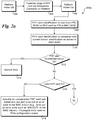
- operations and logic to configure a mezzanine PHY card and MAC during platform initialization operations proceed as follows. First, in a block 202, the platform power is off. The customer/user then plugs in the PHY card into the mezzanine connector on the platform, as shown in a block 204. The platform is then powered on in a block 206, which initiates the platform's normal boot-up processes.
- the PHY card identification is read from FRU NVM on the PHY card by MAC firmware.
- instructions stored in firmware 112 in MAC NVM 110 are executed on one of the processor cores on SoC/PCH 102 (not shown in Figures 1 and 1a ), or otherwise by a processing component that is used during the platform's pre-boot process.
- the PHY card ID is stored as a PHY card per implementation ID 300 in FRU 118 (referred to a PHY card ID 300 below).
- the PHY card ID is compared with a current known PHY card ID, as stored in MAC NVM 110 as current PHY card ID 114.
- the current known PHY card ID corresponds to the PHY card ID that was most recently installed in the platform.
- a decision block 212 a determination is made to whether PHY card ID 300 matches current PHY card ID 114. Since this is the first boot after a new mezzanine PHY card is installed, there will be either no PHY card ID value stored for current PHY card ID 114, or the current PHY card ID value will be different than PHY card ID 300 (for instances under which the mezzanine PHY card is a replacement for a previously installed PHY card). Accordingly, the answer to decision block 212 is NO, and the logic proceeds to a decision block 216 in which a determination is made to whether the PHY card ID is valid.
- SoC/PCH 102 maintains a list of valid PHY card IDs in PHY configuration data 116.
- PHY configuration data 116 Generally, a given SoC or PCH model or SKU (Stock Keeping Unit) will be configured to support various PHY card configurations and capabilities, and include a list of PHY card IDs that it supports.
- This PHY card ID list may generally be written to PHY configuration data 116 during SoC or PCH manufacture or system integration.
- the PHY configuration data may be updated in the field or otherwise updated subsequent to manufacture or system integration to support new PHY cards with PHY card IDs that currently aren't in the list.
- the answer to decision block 216 is NO, and the logic proceeds to a block 218.
- block 218 in one embodiment it is assumed that an unsupported PHY card was added, and the process exits and writes out an error code to the MAC silicon, such as writing out an "ENOSYS" error code.
- the error code is propagated to the PCIe (Peripheral Component Interconnect Express) configuration space, which enables logic used for enumerating and configuring PCIe devices to recognize that the PHY card is unsupported, and thus not configure it to be accessed by the platform.
- PCIe Peripheral Component Interconnect Express
- FIG. 3 shows some of the configuration parameters used by one embodiment, which includes the number of physical functions 302 for the MAC that are exposed to the PHY card, the number of ports 304, a set of port device IDs 306 (one for each port), a set of port subdevice IDs 308 (one for each port), a set of port configuration type IDs 310 (one for each port), and IO Fabric/PCIe memory base address registers (BARs) 312.
- BARs IO Fabric/PCIe memory base address registers
- the configuration parameters that are read from the FRU NVM include the number of physical functions 302 for the MAC that are supported by the PHY card, the number of ports, the PCIe device IDs 306, subdevice IDs 308 and connection type IDs 310 for each port of the PHY card and the order in which they are enumerated/assigned, and IO Fabric/PCIe memory BARs 312.
- the configuration values read from the FRU NVM are programmed into the MAC silicon's PCIe configuration space. In one embodiment, default PCIe configuration information is built into the MAC silicon, but can be overridden by the MAC NVM.
- firmware 112 uses the PHY card ID to select the correct PHY configuration firmware script from PHY configuration data 116.
- the selected PHY configuration script is loaded and executed over side band interface 136, which results in configuration of the PHY card. Once configured, the PHY card initiates link negotiation for each of its ports via the media connector for each port, as shown in a block 228.
- PCIe device enumeration and configuration configuration data is read by a PCIe Root Complex to enumerate the PCIe interconnect hierarchy and PCIe devices coupled to the PCI interconnect segments in the hierarchy.
- configuration data is read by a PCIe Root Complex to enumerate the PCIe interconnect hierarchy and PCIe devices coupled to the PCI interconnect segments in the hierarchy.
- the MAC silicon's PCIe configuration space is read.
- the PCIe configuration data in the PCIe configuration space is formatted to enable the PCIe Root Complex to enumerate the PHY ports and/or physical functions supported by the mezzanine PHY card, which are enumerated as respective PCI devices.
- this PCIe configuration data is read by the operating system, thereby exposing the mezzanine PHY cards ports/physical functions to the OS and making them available for access by software running on the platform.
- the split MAC-PHY layer implementation is transparent to the platform's host operating system. Rather, from the standpoint of the OS, it simply sees a NIC card (or other communication protocol card) supporting one or more PCIe device functions.
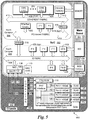
- FIGS 4 and 5 show exemplary platform architectures 400 and 500 the support use of mezzanine PHY cards in accordance with aspects of the embodiments described herein.
- platform architecture 400 includes a processor SoC 402 and a PCH 404 mounted on a main board 405 and coupled to one another via interconnected wiring in the main board.
- Processor SoC 402 includes a CPU (central processor unit) 406 including a plurality of processor cores 408 coupled to a coherent fabric 410.
- Each of cores 408 includes a Level 1 (L1) and Level 2 (L2) cache.
- a memory controller 412 is also coupled to coherent fabric 410, and is configured to provide access to system memory 413 (e.g ., a type of Dynamic Random Access Memory (DRAM)) via one or more memory channels.
- system memory 413 e.g ., a type of Dynamic Random Access Memory (DRAM)
- DRAM Dynamic Random Access Memory
- a last level cache (LLC) may also be coupled to coherent fabric 410 (not shown), and, along with various cache agents in the like (also not shown), the L1/L2 caches, LLC, and memory 414 form a coherent memory domain.
- a PCI-based fabric 414 (e.g. , a 3rd generation PCIe fabric) is coupled to coherent fabric 410 via a fabric-to-fabric bridge 416.
- IP Intellectual Property
- a PCIe Root Complex 420 is also coupled to PCI-based fabric 414.
- PCI-based Fabric is shown as a single fabric segment, but may comprise multiple fabric segments in a PCI-based hierarchy, as is well-known in the art.
- Processor SoC 402 may be communicatively coupled to PCH 404 via various types of interconnects and corresponding interfaces.
- an interconnect 422 is depicted as being connected between a PCH interface 424 and a processor interface 426.
- both PCH interface 424 and a processor interface 426 will share the same link interface on the interconnect side, while being configured to interface to the respective fabrics to which each of PCH interface 424 and a processor interface 426 is coupled.
- interconnect 422 comprises a Quickpath Interconnect (QPITM) link, a Keizer Technology Interconnect (KTI) link, an Ultrapath Interconnect (UPI) link, a Direct Media Interface (DMI) link, or any type of existing or future high-speed chip-to-chip interconnect.
- QPITM Quickpath Interconnect
- KTI Keizer Technology Interconnect
- UPI Ultrapath Interconnect
- DMI Direct Media Interface
- PCH 404 includes an IO (Input/Output) fabric 428 to which various IP blocks 430 are coupled, as depicted by IP 3, IP 4, IP 5, and IP 6.
- IP blocks 430 may be configured to perform one or more functions and/or may comprise an interface to a component that is external to PCH 404.
- IP blocks 430 may include but are not limited to PCIe interfaces, USB (Universal Serial Bus) interfaces, General Purpose IO (GPIO), System Management Bus (SMBus) interfaces, high definition audio, power management, low pin count (LPC) interfaces, SPI, video display interfaces, system management interfaces, and JTAG interfaces.
- Additional IP blocks coupled to IO fabric 428 that are specifically depicted in Figure 4 include a Serial ATA interface 432 coupled to a solid state drive (SSD) 434, a firmware interface 436 coupled to BIOS/firmware 438, and a PCIe Root Complex 440.
- SSD solid state drive
- firmware interface 436 coupled to BIOS/firmware 438
- PCIe Root Complex 440 PCIe Root Complex
- PCH 404 further includes a MAC block 108 coupled to a MAC NVM 110 and including a MAC-to-PHY interface 109.
- MAC-to-PHY interface 109 is coupled to various pins on a connector 106 to which a mezzanine card 104a is also coupled, enabled TX data, RX data and side band signals to be passed between MAC block 108 and components on mezzanine card 104a, including FRU NVM 118 and PHY interface 138a.
- connector 106 is mounted to a mezzanine "shelf or the like in a chassis 422, and signals corresponding to the TX data, RX data, and sideband signals are coupled between connector 106 and PCH 404 via one or more cables and/or applicable wiring and vias formed in main board 405 and another board to which connector 106 is mounted.
- a processor SoC 502 is mounted on a main board 504 and is communicatively coupled to a Mezzanine PHY card 104a via a connector 106 and applicable signal routing means (e.g ., cabling and/or wiring paths/vias in main board 504).
- processor SoC 502 implements the functionality of selected PCH blocks on the same SoC as the processor core components and interconnects.
- the upper portion of processor SoC 502 is part of a "North" complex 506, while the bottom portion is part of a "South” complex 508.
- the North and South complex names are a variation of the historical North Bridge (processor) and South Bridge (PCH) found in platform chipsets developed by INTEL® Corporation.
- SoC 502 employs a bridge 510 that is coupled between PCI-based fabric 414 and IO fabric 428.
- architecture 500 employs BIOS/Firmware 438a, which is similar to BIOS/Firmware 438 with some differences accounting for the different IP blocks in architectures 400 and 500.
- IO fabric 428 may comprise any of various types of existing and future IO fabrics and/or interconnect structures, including but not limited to PCIe, INTEL® On-chip Scalable Fabric (IOSF), Open Core Protocol (OCP), Advanced Microcontroller Bus Architecture (AMBA) (e.g ., Advanced High-performance Bus (AHB)), and Basic Virtual Component Interface (BVCI) interconnects.
- PCIe INTEL® On-chip Scalable Fabric
- OCP Open Core Protocol
- AMBA Advanced Microcontroller Bus Architecture
- AHB Advanced High-performance Bus
- BVCI Basic Virtual Component Interface
- embodiments of this invention may be used as or to support a software program, software modules, firmware, and/or distributed software executed upon some form of processor, processing core or embedded logic a virtual machine running on a processor or core or otherwise implemented or realized upon or within a computer-readable or machine-readable non-transitory storage medium.
- a computer-readable or machine-readable non-transitory storage medium includes any mechanism for storing or transmitting information in a form readable by a machine (e.g. , a computer).
- a computer-readable or machine-readable non-transitory storage medium includes any mechanism that provides (i.e ., stores and/or transmits) information in a form accessible by a computer or computing machine (e.g. , computing device, electronic system, etc .), such as recordable/non-recordable media (e.g. , read only memory (ROM), random access memory (RAM), magnetic disk storage media, optical storage media, flash memory devices, etc .).
- the content may be directly executable ("object” or “executable” form), source code, or difference code (“delta" or "patch” code).
- a computer-readable or machine-readable non-transitory storage medium may also include a storage or database from which content can be downloaded.
- the computer-readable or machine-readable non-transitory storage medium may also include a device or product having content stored thereon at a time of sale or delivery.
- delivering a device with stored content, or offering content for download over a communication medium may be understood as providing an article of manufacture comprising a computer-readable or machine-readable non-transitory storage medium with such content described herein.
- Various components referred to above as processes, servers, or tools described herein may be a means for performing the functions described.
- the operations and functions performed by various components described herein may be implemented by software running on a processing element, via embedded hardware or the like, or any combination of hardware and software.
- Such components may be implemented as software modules, hardware modules, special-purpose hardware (e.g. , application specific hardware, ASICs, DSPs, etc .), embedded controllers, hardwired circuitry, hardware logic, etc.
- Software content e.g. , data, instructions, configuration information, etc .
Landscapes
- Engineering & Computer Science (AREA)
- Theoretical Computer Science (AREA)
- General Engineering & Computer Science (AREA)
- Physics & Mathematics (AREA)
- General Physics & Mathematics (AREA)
- Software Systems (AREA)
- Computer Hardware Design (AREA)
- Computer Security & Cryptography (AREA)
- Computer Networks & Wireless Communication (AREA)
- Signal Processing (AREA)
- Information Transfer Systems (AREA)
- Computer And Data Communications (AREA)
Description
- In recent years, there has been tremendous growth in "cloud-hosted" computing and services, which are typically facilitated through large data centers. Examples of cloud-hosted services include AMAZON Web Services (AWS™) and Elastic Compute Cloud (EC2), MICROSOFT Azure™ and Office 365™, APPLE iCloud™, various GOOGLE services (e.g ., Google Docs™), and online e-mail services such MICROSOFT Hotmail™ (now Outlook Online™), YAHOO mail, and GOOGLE gmail™, as well as a plethora of small e-mail services. In addition, many eCommerce sites are hosted on third-party operated data centers (e.g ., AWS hosts a large number of eCommerce sites, in addition to Amazon.com itself). Streaming media services such as those provided by NETFLIX and YOUTUBE are also hosted by large data centers. Continued exponential growth of cloud-hosted services is expected for the foreseeable future.
- Common criteria for data center hardware include flexibility and ease of install and configuration. For example, much of today's data center compute resources (e.g ., rack and blade servers) are virtualized, enabling rapid deployment and migration of services, as well as reducing services (and their host hardware energy consumption) during periods of low utilization. It is also preferable that servers and the like be easily configurable. For instance, it is common to have "plug-and-play" (PnP) support for various add-on cards and peripherals, such as network cards and network interface controllers (NICs). Under plug-and-play, a PnP card or peripheral can be automatically configured (or otherwise configured with relative ease).
- Recently, members of the Open Compute Project (OCP) has published specifications defining the use of OCP mezzanine cards in OCP Open Rack and other types of servers (available at http://www.opencompute.org/wiki/Server/SpecsAndDesigns) One of the OCP specifications defines a mezzanine form factor for NIC cards. The specification defines support for mezzanine NIC cards with multiple ports and various types of Physical interfaces (PHYs).
- In
US 8 069 293 B1 a system allowing a flexible upgrade of a computer system (e.g. server) to a high-speed network connection comprises base configuration motherboard or network card including a set of low-speed (e.g. 1 Gbps Ethernet) media access controllers (MACs) each connected to a low-speed physical controller (PHY), and a set of high-speed (e.g. 10 Gbps Ethernet) MACs. An expansion card including high-speed PHYs of choice can be connected by an end user to the base configuration motherboard or network card. A flow classifier classifies data sent/received over both high-speed and low-speed ports, and a single driver may control both high- and low-speed ports. One or both of the motherboard and/or expansion card are configured according to a detected type (e.g. physical layer standard, vendor) of expansion card connected to the motherboard and/or type of physical medium connected to the expansion card. - In
US 2012/030730 A1 a processor can enforce a blacklist and validate, according to a multi-phase lockstep integrity protocol, a device coupled to the processor. Such enforcement may prevent the device from accessing one or more resources of a system prior to the validation. The blacklist may include a list of devices that have not been validated according to the multi-phase lockstep integrity protocol. - In
US 2009/164628 A1 an integrated circuit is disclosed, including at least one configuration pin, an interface circuit, a detecting circuit, a determining circuit and a storage unit. A physical layer circuit of the invention not only increases the flexibility of setting PHY addresses, but also reduces the number of configuration pins. -
EP 1 133 129 A2 - The foregoing aspects and many of the attendant advantages of this invention will become more readily appreciated as the same becomes better understood by reference to the following detailed description, when taken in conjunction with the accompanying drawings, wherein like reference numerals refer to like parts throughout the various views unless otherwise specified:
-
Figure 1 is a schematic diagram illustrating a platform including an SoC/PCH with an integrated MAC block communicatively coupled to a mezzanine PHY card, according to one embodiment; -
Figure 1a is a schematic diagram illustrating a platform including an SoC/PCH with an integrated MAC block communicatively coupled to a mezzanine PHY card including two 10 Gb Ethernet ports and two 40 Gb Ethernet ports, according to one embodiment; -
Figures 2a and2b collectively comprises a flowchart illustrating operations and logic implemented during pre-boot operations to configured implementation of a mezzanine PHY card in a computer platfrom, according to one embodiment; -
Figure 3 is a schematic block diagram illustrating an exemplary set of configuration parameters and data stored in an FRU NVM, according to one embodiment -
Figure 4 is a schematic diagram illustrating a platform architecture employing a processor SoC coupled to a PCH with an integrated MAC block that is communicatively coupled to a Mezzanine PHY card, according to one embodiment; and -
Figure 5 is a schematic diagram illustrating a platform architecture employing a processor SoC with an integrated MAC block that is communicatively coupled to a Mezzanine PHY card, according to one embodiment. - The present invention is defined in the independent claims. Embodiments of methods for implement mini-mezzanine Open Compute Project (OCP) plug-and-play Network PHY Cards and associated apparatus are described herein.
- As discussed above, the Open Compute Project has published a specification for implementing a mezzanine card form factor for NIC cards. Under one type of use case, the mezzanine NIC card is similar to conventional NIC card (in terms of functionality), except it has a different form factor and physical connection, and operates as a standalone plug-and-play product. In addition, INTEL® Corporation is developing some new System on a Chip (SoC) processor and Platform Controller Hub (PCH) architectures that integrate Media Access Control (MAC) layer functionary on the SoC or PCH and including a MAC/PHY interface. To take advantage of this architecture in server platforms supporting mezzanine NIC cards, a variant of the mezzanine NIC card is being developed that only includes one or more PHYs and an interface that is configured to connect to the MAC/PHY interface on the SOC/PCH with integrated MACs.
- An exemplary implementation of this scheme is illustrated in
Figure 1 , which shows aplatform 100 including an SoC/PHC 102 coupled to amezzanine PHY card 104, via aconnector 106. SoC/PCH 102 includes aMAC block 108 coupled to a MAC non-volatile memory (NVM) 110.MAC block 108 includes circuitry and logic for implementing MAC layer functionality, which would typically implemented on a NIC or NIC card (aka network adapter) under a conventional configuration.MAC block 108 also includes a MAC-to-PHY interface 109. MAC NVM 110 includes firmware (FW) 112, a currentPHY card ID 114, andPHY configuration data 116. -
Mezzanine PHY card 104 is a field replaceable unit (FRU) that can be installed in a mezzanine card slot of an appropriately configured platform, such as defined in the OCP mezzanine card specification discussed above. In the illustrated embodiment,mezzanine PHY card 104 includes an FRUNVM 118 and a third-party physical layer part (PHY) 120 that is configured to implement PHY operations for one or more different types of physical media. In one embodiment PHY 120 is a standalone chip mounted to a circuit board to which a non-volatile memory device corresponding to FRU NVM 118, such as a Flash chip, is also mounted. Optionally, FRU NVM or similar non-volatile storage circuitry maybe be integrated on aPHY 120 chip. - PHY 120 is depicted as being coupled to multiple connectors that are illustrative of an exemplary, but non-limiting set of types of physical media, including an SFP+ (enhanced Small Form-factor, Pluggable)
connector 122, an RJ45 Ethernetconnector 124, a generic mediaphysical connector 126, and a QSFP+ (enhanced Quad Small Form-factor Pluggable)connector 128. Although not show for simplicity inFigure 1 , PHY 120 would include circuitry and logic configured to implement PHY layer operations in accordance with applicable standardized physical media specifications associated with each type of physical media that is to be supported bymezzanine PHY card 104. - Various signals are depicted being passed between SoC/
PCH 102 andmezzanine PHY card 104 viaconnector 106. These includesideband signals 130, data transmit (TX)signals 132, data receive (RX)signals 134, andsideband signals 136. Generally, various electronic pathways may be used for these signals, such as traces and vias in printed circuit boards (PCBs) and cables. - In the embodiment illustrated in
Figure 1 ,PHY 120 is depicted as including aPHY interface 138. Depending on the particular physical media, a PHY will typically include multiple layers, with the top layer interfacing with the bottom layer of the MAC. In some embodiments, such as various high speed Ethernet standards, a reconciliation layer sits between the top PHY layer and the MAC. As another option, a MAC-to-PHY interface may be implemented inPHY 120, in which case MAC-to-PHY interface 109 would be a MAC interface (not shown). Generally, the reconciliation layer, if applicable, may be implemented on any of a MAC interface, a PHY interface, or a MAC-to-PHY interface (not shown). - Generally, the combination of functionality provided by the MAC block and PHY card will support the MAC and PHY layer functionality associated with a multi-layer communication protocol stack including MAC and PHY layers. Moreover, and given MAC block and PHY card may be configured to support the MAC and PHY layer functionality associated with multiple communication protocol stacks, including different communication protocol stacks.
-
Figure 1a shows aplatform 100a that includes amezzanine PHY card 104a providing four high-speed Ethernet ports.Ports ports ports ports 10Gb Ethernet ports RJ45 connectors 40Gb Ethernet ports 40GbE connectors 10Gb Ethernet ports 40Gb Ethernet ports PHY interface 138a. - In one embodiment,
10Gb Ethernet ports 40Gb Ethernet ports - In addition to the Ethernet communication protocol, other multi-layer communication protocols and fabrics may also be supported, including FibreChannel, InfiniBand, INTEL® OmniPath Architecture fabric, SONET, TCP/IP, UDP, etc. Generally, the techniques disclosed herein are not limited to a specific protocol or set of protocols.
- With reference to
flowchart portions Figures 2a and2b , operations and logic to configure a mezzanine PHY card and MAC during platform initialization operations, according to one embodiment, proceed as follows. First, in a block 202, the platform power is off. The customer/user then plugs in the PHY card into the mezzanine connector on the platform, as shown in a block 204. The platform is then powered on in ablock 206, which initiates the platform's normal boot-up processes. - In a
block 208, the PHY card identification (ID) is read from FRU NVM on the PHY card by MAC firmware. In one embodiment, instructions stored infirmware 112 inMAC NVM 110 are executed on one of the processor cores on SoC/PCH 102 (not shown inFigures 1 and1a ), or otherwise by a processing component that is used during the platform's pre-boot process. As shown inFigure 3 , in one embodiment the PHY card ID is stored as a PHY card perimplementation ID 300 in FRU 118 (referred to aPHY card ID 300 below). - In a block 210, the PHY card ID is compared with a current known PHY card ID, as stored in
MAC NVM 110 as currentPHY card ID 114. The current known PHY card ID corresponds to the PHY card ID that was most recently installed in the platform. In adecision block 212, a determination is made to whetherPHY card ID 300 matches currentPHY card ID 114. Since this is the first boot after a new mezzanine PHY card is installed, there will be either no PHY card ID value stored for currentPHY card ID 114, or the current PHY card ID value will be different than PHY card ID 300 (for instances under which the mezzanine PHY card is a replacement for a previously installed PHY card). Accordingly, the answer to decision block 212 is NO, and the logic proceeds to adecision block 216 in which a determination is made to whether the PHY card ID is valid. - In one embodiment, SoC/
PCH 102 maintains a list of valid PHY card IDs inPHY configuration data 116. Generally, a given SoC or PCH model or SKU (Stock Keeping Unit) will be configured to support various PHY card configurations and capabilities, and include a list of PHY card IDs that it supports. This PHY card ID list may generally be written toPHY configuration data 116 during SoC or PCH manufacture or system integration. In addition, the PHY configuration data may be updated in the field or otherwise updated subsequent to manufacture or system integration to support new PHY cards with PHY card IDs that currently aren't in the list. - If the PHY card ID is not valid (e.g ., not in the list of PHY card IDs stored in configuration data 116), the answer to decision block 216 is NO, and the logic proceeds to a
block 218. Inblock 218, in one embodiment it is assumed that an unsupported PHY card was added, and the process exits and writes out an error code to the MAC silicon, such as writing out an "ENOSYS" error code. In one embodiment, the error code is propagated to the PCIe (Peripheral Component Interconnect Express) configuration space, which enables logic used for enumerating and configuring PCIe devices to recognize that the PHY card is unsupported, and thus not configure it to be accessed by the platform. - If the PHY card ID is valid, the answer to decision block 216 is YES, and the logic proceeds to the
portion 200b of the flowchart shown inFigure 2b . In ablock 220, various configuration parameters are read from the FRU NVM.Figure 3 shows some of the configuration parameters used by one embodiment, which includes the number ofphysical functions 302 for the MAC that are exposed to the PHY card, the number of ports 304, a set of port device IDs 306 (one for each port), a set of port subdevice IDs 308 (one for each port), a set of port configuration type IDs 310 (one for each port), and IO Fabric/PCIe memory base address registers (BARs) 312. It is noted that the set of configuration parameters illustrated inFigure 3 is merely exemplary and non-limiting, as other types of configuration parameters and data may also be stored in in an FRU NVM - Returning to block 220, in the illustrated embodiment the configuration parameters that are read from the FRU NVM include the number of
physical functions 302 for the MAC that are supported by the PHY card, the number of ports, thePCIe device IDs 306,subdevice IDs 308 andconnection type IDs 310 for each port of the PHY card and the order in which they are enumerated/assigned, and IO Fabric/PCIe memory BARs 312. - In a
block 222, the configuration values read from the FRU NVM are programmed into the MAC silicon's PCIe configuration space. In one embodiment, default PCIe configuration information is built into the MAC silicon, but can be overridden by the MAC NVM. In a block 224,firmware 112 uses the PHY card ID to select the correct PHY configuration firmware script fromPHY configuration data 116. Next, in ablock 226, the selected PHY configuration script is loaded and executed overside band interface 136, which results in configuration of the PHY card. Once configured, the PHY card initiates link negotiation for each of its ports via the media connector for each port, as shown in a block 228. - Each of the foregoing operations is performed during "pre-boot" processes prior to PCIe device enumeration and configuration. During PCIe device enumeration and configuration, configuration data is read by a PCIe Root Complex to enumerate the PCIe interconnect hierarchy and PCIe devices coupled to the PCI interconnect segments in the hierarchy. As part of this operation, in a
block 230 the MAC silicon's PCIe configuration space is read. The PCIe configuration data in the PCIe configuration space is formatted to enable the PCIe Root Complex to enumerate the PHY ports and/or physical functions supported by the mezzanine PHY card, which are enumerated as respective PCI devices. As part of the PCIe configuration process, this PCIe configuration data is read by the operating system, thereby exposing the mezzanine PHY cards ports/physical functions to the OS and making them available for access by software running on the platform. - The enumeration and identification of PCIe devices, in combination with compatible OS drivers, enables the inherent plug-and-play functionality supported by the PCIe architecture. Under the embodiments herein, the split MAC-PHY layer implementation is transparent to the platform's host operating system. Rather, from the standpoint of the OS, it simply sees a NIC card (or other communication protocol card) supporting one or more PCIe device functions.
-
Figures 4 and5 showexemplary platform architectures Figure 4 ,platform architecture 400 includes aprocessor SoC 402 and aPCH 404 mounted on amain board 405 and coupled to one another via interconnected wiring in the main board.Processor SoC 402 includes a CPU (central processor unit) 406 including a plurality ofprocessor cores 408 coupled to acoherent fabric 410. Each ofcores 408 includes a Level 1 (L1) and Level 2 (L2) cache. Amemory controller 412 is also coupled tocoherent fabric 410, and is configured to provide access to system memory 413 (e.g ., a type of Dynamic Random Access Memory (DRAM)) via one or more memory channels. A last level cache (LLC) may also be coupled to coherent fabric 410 (not shown), and, along with various cache agents in the like (also not shown), the L1/L2 caches, LLC, andmemory 414 form a coherent memory domain. - A PCI-based fabric 414 (e.g. , a 3rd generation PCIe fabric) is coupled to
coherent fabric 410 via a fabric-to-fabric bridge 416. Various Intellectual Property (IP) blocks 418 are coupled to PCI-basedfabric 414, is depicted by IP blocks labeledIP 1 andIP 2. APCIe Root Complex 420 is also coupled to PCI-basedfabric 414. For simplicity, PCI-based Fabric is shown as a single fabric segment, but may comprise multiple fabric segments in a PCI-based hierarchy, as is well-known in the art. -
Processor SoC 402 may be communicatively coupled toPCH 404 via various types of interconnects and corresponding interfaces. For simplicity, aninterconnect 422 is depicted as being connected between aPCH interface 424 and aprocessor interface 426. In a typical implementation, bothPCH interface 424 and aprocessor interface 426 will share the same link interface on the interconnect side, while being configured to interface to the respective fabrics to which each ofPCH interface 424 and aprocessor interface 426 is coupled. Under various embodiments,interconnect 422 comprises a Quickpath Interconnect (QPI™) link, a Keizer Technology Interconnect (KTI) link, an Ultrapath Interconnect (UPI) link, a Direct Media Interface (DMI) link, or any type of existing or future high-speed chip-to-chip interconnect. - In addition to
processor interface 426,PCH 404 includes an IO (Input/Output)fabric 428 to whichvarious IP blocks 430 are coupled, as depicted byIP 3,IP 4,IP 5, andIP 6. Each of IP blocks 430 may be configured to perform one or more functions and/or may comprise an interface to a component that is external toPCH 404. For example, IP blocks 430 may include but are not limited to PCIe interfaces, USB (Universal Serial Bus) interfaces, General Purpose IO (GPIO), System Management Bus (SMBus) interfaces, high definition audio, power management, low pin count (LPC) interfaces, SPI, video display interfaces, system management interfaces, and JTAG interfaces. Additional IP blocks coupled toIO fabric 428 that are specifically depicted inFigure 4 include aSerial ATA interface 432 coupled to a solid state drive (SSD) 434, afirmware interface 436 coupled to BIOS/firmware 438, and aPCIe Root Complex 440. -
PCH 404 further includes aMAC block 108 coupled to aMAC NVM 110 and including a MAC-to-PHY interface 109. MAC-to-PHY interface 109 is coupled to various pins on aconnector 106 to which amezzanine card 104a is also coupled, enabled TX data, RX data and side band signals to be passed between MAC block 108 and components onmezzanine card 104a, includingFRU NVM 118 andPHY interface 138a. In one embodiment,connector 106 is mounted to a mezzanine "shelf or the like in achassis 422, and signals corresponding to the TX data, RX data, and sideband signals are coupled betweenconnector 106 andPCH 404 via one or more cables and/or applicable wiring and vias formed inmain board 405 and another board to whichconnector 106 is mounted. - In
platform architecture 500 ofFigure 5 , aprocessor SoC 502 is mounted on amain board 504 and is communicatively coupled to aMezzanine PHY card 104a via aconnector 106 and applicable signal routing means (e.g ., cabling and/or wiring paths/vias in main board 504). Rather than have a separate processor SoC and a PCH,processor SoC 502 implements the functionality of selected PCH blocks on the same SoC as the processor core components and interconnects. As illustrated, the upper portion ofprocessor SoC 502 is part of a "North" complex 506, while the bottom portion is part of a "South" complex 508. The North and South complex names are a variation of the historical North Bridge (processor) and South Bridge (PCH) found in platform chipsets developed by INTEL® Corporation. - Generally, components in each of North complex 506 and South complex 508 sharing the same reference number of components in
SoC 402 andPCH 404 ofFigure 4 are configured in a similar manner and perform similar functions. As further shown inFigure 5 ,SoC 502 employs abridge 510 that is coupled between PCI-basedfabric 414 andIO fabric 428. In addition,architecture 500 employs BIOS/Firmware 438a, which is similar to BIOS/Firmware 438 with some differences accounting for the different IP blocks inarchitectures - Generally,
IO fabric 428 may comprise any of various types of existing and future IO fabrics and/or interconnect structures, including but not limited to PCIe, INTEL® On-chip Scalable Fabric (IOSF), Open Core Protocol (OCP), Advanced Microcontroller Bus Architecture (AMBA) (e.g ., Advanced High-performance Bus (AHB)), and Basic Virtual Component Interface (BVCI) interconnects. - As discussed above, various aspects of the embodiments herein may be facilitated by corresponding software and/or firmware components and applications, such as software and/or firmware executed by an embedded processor or the like. Thus, embodiments of this invention may be used as or to support a software program, software modules, firmware, and/or distributed software executed upon some form of processor, processing core or embedded logic a virtual machine running on a processor or core or otherwise implemented or realized upon or within a computer-readable or machine-readable non-transitory storage medium. A computer-readable or machine-readable non-transitory storage medium includes any mechanism for storing or transmitting information in a form readable by a machine (e.g. , a computer). For example, a computer-readable or machine-readable non-transitory storage medium includes any mechanism that provides (i.e ., stores and/or transmits) information in a form accessible by a computer or computing machine (e.g. , computing device, electronic system, etc .), such as recordable/non-recordable media (e.g. , read only memory (ROM), random access memory (RAM), magnetic disk storage media, optical storage media, flash memory devices, etc .). The content may be directly executable ("object" or "executable" form), source code, or difference code ("delta" or "patch" code). A computer-readable or machine-readable non-transitory storage medium may also include a storage or database from which content can be downloaded. The computer-readable or machine-readable non-transitory storage medium may also include a device or product having content stored thereon at a time of sale or delivery. Thus, delivering a device with stored content, or offering content for download over a communication medium may be understood as providing an article of manufacture comprising a computer-readable or machine-readable non-transitory storage medium with such content described herein.
- Various components referred to above as processes, servers, or tools described herein may be a means for performing the functions described. The operations and functions performed by various components described herein may be implemented by software running on a processing element, via embedded hardware or the like, or any combination of hardware and software. Such components may be implemented as software modules, hardware modules, special-purpose hardware (e.g. , application specific hardware, ASICs, DSPs, etc .), embedded controllers, hardwired circuitry, hardware logic, etc. Software content (e.g. , data, instructions, configuration information, etc .) may be provided via an article of manufacture including computer-readable or machine-readable non-transitory storage medium, which provides content that represents instructions that can be executed. The content may result in a computer performing various functions/operations described herein.
Claims (11)
- A method, comprising:reading PHY card configuration data stored on a PHY card (104; 104a) including a PHY card identifier, ID, (300) the PHY card (104; 104a) installed in a computer platform (100; 100a; 400; 500) including at least one port (140, 142, 144, 146) and configured to support Physical layer functionality associated with at least one communication protocol stacks and to communicate with a Media Access Control, MAC, block (108) configured to support MAC layer functionality for the at least one communication protocol stack, the MAC block (108) implemented in an integrated circuit, IC, component (102) in the computer platform (100; 100a; 400; 500) that is separate from the PHY card (104; 104a);comparing the PHY card ID (300) to a list of valid PHY card IDs to determine whether the PHY card (104; 104a) is a valid PHY card, wherein a valid PHY card ID is a PHY card ID in the list of PHY card IDs stored in PHY configuration data (116) that is stored in non-volatile memory (110) included in the IC component (102); andif the PHY card (104; 104a) is determined to be a valid PHY card, configuring the PHY card (104; 104a) to implement Physical layer functionality associated with the at least one communication protocol stack for at least one port (140, 142, 144, 146),wherein the method further comprises:storing a PHY configuration script for at least one PHY card (104; 104a);selecting a PHY configuration script based on the PHY card ID (300) that is read; andexecuting the PHY configuration script to configure the PHY card (104; 104a).
- The method of claim 1, further comprising:reading configuration parameters from the PHY card (104; 104a), including a number of ports (304) provided by the PHY card (104; 104a), and at least one of a device and subdevice ID for each port (140, 142, 144, 146); andprogramming Peripheral Component Interconnect Express, PCIe, configuration parameters corresponding to the configuration parameters that are read into a PCIe configuration space associated with the MAC block (108).
- The method of claim 1 or 2, further comprising reading the PCIe configuration parameters and enumerating one or more PCIe devices corresponding to Physical functions supported by the PHY card (104; 104a).
- The method of any of claims 1-3, further comprising:storing a current PHY card identifier, ID, (114) corresponding to a PHY card (104; 104a) installed in the computer platform (100; 100a; 400; 500) on the IC component (102);during a subsequent initialization of the compute platform (100; 100a; 400; 500),reading a PHY card identifier, ID, (300) stored on the PHY card (104; 104a);comparing the PHY card ID (300) that is read to the current PHY card ID (114) that is stored, and if the PHY card ID (300) matches the current PHY card ID (114), using the PCIe configuration parameters programmed into the PCIe configuration space.
- An integrated circuit, IC, configured to be installed in a computer platform (100; 100a; 400; 500) including a PHY card (104; 104a), comprising:a media access control, MAC, block, (108) configured to implement MAC layer functionality associated with one or more communication protocol stacks including a Physical layer, PHY;an interface (109), configured to couple signals between the MAC block (108) and the PHY card (104; 104a) when the IC (102) is installed in the computer platform (100; 100a; 400; 500), the PHY card (104; 104a) including at least one port (140, 142, 144, 146) and configured to support Physical layer functionality associated with at least one communication protocol stack among the one or more communication protocol stacks; andfirmware instructions, stored on the IC (102), configured to be executed by one of a processing element on the IC or on a processing element in a processor to which the IC (102) is configured to be coupled to when installed in the computer platform (100; 100a; 400; 500), the firmware instructions coded, upon execution, to configure the PHY card (104; 104a) for use in the computer platform (100; 100a; 400; 500),wherein the IC (102) further includes non-volatile memory (110), and wherein the firmware instructions, when executed, are configured to cause the IC (102) to:read PHY card configuration data stored on the PHY card (104; 104a) including a PHY card identifier, ID, (300);compare the PHY card ID (300) to a list of valid PHY card IDs, wherein a valid PHY card ID is a PHY card ID in the list of PHY card IDs stored in PHY configuration data (116) stored in the non-volatile memory (110) to determine whether the PHY card (104; 104a) is supported by the IC (102); andif the PHY card (104; 104a) is determined to be a valid PHY card, configure the PHY card (104; 104a) to implement Physical layer functionality associated with the at least one communication protocol stack for at least one port (140, 142, 144, 146),wherein the firmware instructions, when executed, are further configured to cause the IC (102) to:store a PHY configuration script for at least one PHY card (104; 104a);select a PHY configuration script based on the PHY card ID (300) that is read; andexecute the PHY configuration script to configure the PHY card (104; 104a).
- The IC of claim 5, wherein the compute platform (100; 100a; 400; 500) includes a mezzanine card slot configured in accordance with an Open Compute Project, OCP, specification, and the PHY card (104; 104a) comprises a mezzanine PHY card configured to be installed the mezzanine card slot.
- The IC of any claim 5 or 6, wherein the firmware instructions, when executed, are further configured to cause the IC (102) to:read configuration parameters from the PHY card (104; 104a), including a number of ports (304) provided by the PHY card (104; 104a), and at least one of a device and subdevice ID for each port (140, 142, 144, 146); andprogram Peripheral Component Interconnect Express, PCIe, configuration parameters corresponding to the configuration parameters that are read into a PCIe configuration space associated with the MAC block (108).
- The IC of claim 7, wherein the firmware instructions, when executed, are configured to cause the IC (102) to:store, on the IC (102), a current PHY card identifier, ID, (114) corresponding to a PHY card currently installed in the computer platform (100; 100a; 400; 500);during a subsequent initialization of the computer platform (100; 100a; 400; 500),read a PHY card identifier, ID, (300) stored on a PHY card (104; 104a) installed in the compute platform (100; 100a; 400; 500) during the subsequent initialization of the computer platform (100; 100a; 400; 500); andcompare the PHY card ID (300) that is read to the current PHY card ID (114) that is stored, and if the PHY card ID (300) matches the current PHY card ID (114), use the PCI configuration parameters programmed into the PCIe configuration space.
- A computer platform comprising:a main board (405; 504);a mezzanine card slot including a connector (106) communicatively coupled to the main board (405; 504);a PHY card (104; 104a), coupled to the connector (106) and installed in the mezzanine card slot, the PHY card (104; 104a) including at least one port (140, 142, 144, 146) and configured to support Physical, PHY, layer functionality associated with at least one communication protocol stack including a media access control, MAC, layer; andan integrated circuit, IC, chip, (102) as defined in any of claims 5-8 mounted on the main board (405; 504) and including,a MAC block (108), configured to implement MAC layer functionality associated with one or more communication protocol stacks including a PHY layer;an interface (109), configured to couple signals between the MAC block (108) and the PHY card (104; 104a) via the connector (106); andfirmware instructions, configured to be executed by one of a processing element on the IC (102) or on a processor to which the IC (102) is configured to be coupled to when installed in the computer platform (100; 100a; 400; 500), the firmware instructions configured, upon execution, to:configure the MAC block (108) and PHY card (104; 104a) for use in the computer platform (100; 100a; 400; 500),read configuration parameters from the PHY card (104; 104a), including a number of ports (304) provided by the PHY card (104; 104a), and at least one of a device and subdevice ID for each port (140, 142, 144, 146); andprogram Peripheral Component Interconnect Express, PCIe, configuration parameters corresponding to the configuration parameters that are read into a PCIe configuration space associated with the MAC block (108),and wherein the computer platform (100; 100a; 400; 500) is configured to read the PCIe configuration parameters and enumerate one or more PCIe devices corresponding to Physical functions supported by the PHY card (104; 104a),wherein the firmware instructions, upon execution, are further configured to:
store a current PHY card identifier, ID, (114) corresponding to a PHY card (104; 104a) installed in the computer platform (100; 100a; 400; 500) on the IC component (102); - The computer platform of claim 9, wherein the IC chip (102) comprises a Platform Controller Hub, PCH,, and the computer platform (100; 100a; 400; 500) further includes a processor to which the PCH is coupled.
- The computer platform of claim 9 or 10, wherein the IC chip (102) comprises a processor System on a Chip, SoC.
Applications Claiming Priority (3)
| Application Number | Priority Date | Filing Date | Title |
|---|---|---|---|
| US14/961,010 US10007634B2 (en) | 2015-12-07 | 2015-12-07 | Method to enable intel mini-mezz open compute project (OCP) plug-and-play network phy cards |
| PCT/US2016/060790 WO2017099917A1 (en) | 2015-12-07 | 2016-11-07 | Method to enable mini-mezzanine open compute project (ocp) plug-and-play network phy cards |
| EP16873540.5A EP3387545A4 (en) | 2015-12-07 | 2016-11-07 | METHOD FOR IMPLEMENTING PHY NETWORK CARDS READY TO USE OPEN MINI-MEZZANINE OPEN COMPUTER PROJECT (OPC) |
Related Parent Applications (1)
| Application Number | Title | Priority Date | Filing Date |
|---|---|---|---|
| EP16873540.5A Division EP3387545A4 (en) | 2015-12-07 | 2016-11-07 | METHOD FOR IMPLEMENTING PHY NETWORK CARDS READY TO USE OPEN MINI-MEZZANINE OPEN COMPUTER PROJECT (OPC) |
Publications (2)
| Publication Number | Publication Date |
|---|---|
| EP3627335A1 EP3627335A1 (en) | 2020-03-25 |
| EP3627335B1 true EP3627335B1 (en) | 2021-06-23 |
Family
ID=58799756
Family Applications (2)
| Application Number | Title | Priority Date | Filing Date |
|---|---|---|---|
| EP19200290.5A Active EP3627335B1 (en) | 2015-12-07 | 2016-11-07 | Method to enable mini-mezzanine open compute project (ocp) plug-and-play network phy cards |
| EP16873540.5A Withdrawn EP3387545A4 (en) | 2015-12-07 | 2016-11-07 | METHOD FOR IMPLEMENTING PHY NETWORK CARDS READY TO USE OPEN MINI-MEZZANINE OPEN COMPUTER PROJECT (OPC) |
Family Applications After (1)
| Application Number | Title | Priority Date | Filing Date |
|---|---|---|---|
| EP16873540.5A Withdrawn EP3387545A4 (en) | 2015-12-07 | 2016-11-07 | METHOD FOR IMPLEMENTING PHY NETWORK CARDS READY TO USE OPEN MINI-MEZZANINE OPEN COMPUTER PROJECT (OPC) |
Country Status (5)
| Country | Link |
|---|---|
| US (1) | US10007634B2 (en) |
| EP (2) | EP3627335B1 (en) |
| KR (1) | KR102757815B1 (en) |
| CN (1) | CN108292289B (en) |
| WO (1) | WO2017099917A1 (en) |
Families Citing this family (24)
| Publication number | Priority date | Publication date | Assignee | Title |
|---|---|---|---|---|
| CN105488009B (en) * | 2015-12-03 | 2018-07-06 | 英业达科技有限公司 | The reading/writing method and read/write system of a kind of FRU |
| US10007634B2 (en) | 2015-12-07 | 2018-06-26 | Intel Corporation | Method to enable intel mini-mezz open compute project (OCP) plug-and-play network phy cards |
| FR3060792B1 (en) * | 2016-12-19 | 2018-12-07 | Safran Electronics & Defense | DATA LOADING DEVICE IN COMPUTERIZED DATA PROCESSING UNITS FROM A DATA SOURCE |
| CN107894809A (en) * | 2017-11-14 | 2018-04-10 | 郑州云海信息技术有限公司 | A kind of road framework interconnecting method of MEZZ card-type four and system |
| KR102079545B1 (en) | 2017-11-20 | 2020-02-20 | (주)케이티엔에프 | Main board equipped with installation parts of Open Compute Project card |
| CN108197064A (en) * | 2018-01-02 | 2018-06-22 | 郑州云海信息技术有限公司 | A kind of onboard network method and device |
| CN108228489A (en) * | 2018-01-02 | 2018-06-29 | 郑州云海信息技术有限公司 | A kind of method that more network interface cards are connected based on OCP standards |
| US11456833B2 (en) | 2018-01-08 | 2022-09-27 | Samsung Electronics Co., Ltd. | Method for separating physical layer functions in wireless communication system |
| CN108848187B (en) * | 2018-07-16 | 2021-03-16 | 苏州浪潮智能科技有限公司 | A method, apparatus, device and readable storage medium for establishing a communication connection |
| US11954326B2 (en) | 2019-02-01 | 2024-04-09 | Liqid Inc. | Memory device instantiation onto communication fabrics |
| US12222890B2 (en) | 2019-02-01 | 2025-02-11 | Liqid Inc. | Programmable logic device configuration over communication fabrics |
| US11392525B2 (en) * | 2019-02-01 | 2022-07-19 | Liqid Inc. | Specialized device instantiation onto PCIe fabrics |
| US12271322B2 (en) | 2019-06-24 | 2025-04-08 | Samsung Electronics Co., Ltd. | Multi-function flexible computational storage device |
| CN111045970B (en) * | 2019-12-18 | 2021-05-11 | 江苏芯盛智能科技有限公司 | A PHY parameter debugging method, device, storage medium and electronic device |
| CN111400217B (en) * | 2020-02-29 | 2021-10-08 | 苏州浪潮智能科技有限公司 | An OCP adapter card and computer equipment |
| CN112822129A (en) * | 2021-02-05 | 2021-05-18 | 井芯微电子技术(天津)有限公司 | PCIe switching equipment |
| US12229073B2 (en) * | 2021-06-07 | 2025-02-18 | Intel Corporation | Systems, apparatus and methods for rapid peripheral component interconnect express (PCIE) system boot |
| US12228915B2 (en) * | 2021-11-05 | 2025-02-18 | Rockwell Automation Technologies, Inc. | Configurable media interface module |
| CN115576765B (en) * | 2022-11-16 | 2023-03-28 | 南京芯驰半导体科技有限公司 | Test method, test device, electronic equipment and storage medium |
| US12444893B2 (en) | 2023-04-27 | 2025-10-14 | Hewlett Packard Enterprise Development Lp | Optimized cable solution |
| KR102671905B1 (en) | 2023-12-29 | 2024-05-31 | 주식회사 티솔루션즈 | Physical layer device that allows selection of heterogeneous communications standards for open platform boards |
| US12457700B2 (en) * | 2024-02-15 | 2025-10-28 | Hewlett Packard Enterprise Development Lp | Removable OCP module with PCIe slots |
| US20260064615A1 (en) * | 2024-08-27 | 2026-03-05 | Qualcomm Incorporated | Apparatus and methods for establishing link bandwidths within die interconnect architectures |
| CN119046198B (en) * | 2024-08-30 | 2025-08-26 | 无锡众星微系统技术有限公司 | A bus interface layered implementation device, method, equipment and medium |
Family Cites Families (25)
| Publication number | Priority date | Publication date | Assignee | Title |
|---|---|---|---|---|
| US6879645B1 (en) * | 1998-09-15 | 2005-04-12 | Tut Systems, Inc. | Method and apparatus for dynamically varying the noise sensitivity of a receiver |
| US6651107B1 (en) * | 1999-09-21 | 2003-11-18 | Intel Corporation | Reduced hardware network adapter and communication |
| US6839345B2 (en) * | 1999-12-17 | 2005-01-04 | Texas Instruments Incorporated | MAC/PHY interface |
| US7352770B1 (en) * | 2000-08-04 | 2008-04-01 | Intellon Corporation | Media access control protocol with priority and contention-free intervals |
| US6731832B2 (en) * | 2001-02-28 | 2004-05-04 | Lambda Opticalsystems Corporation | Detection of module insertion/removal in a modular optical network, and methods and apparatus therefor |
| US20030231649A1 (en) * | 2002-06-13 | 2003-12-18 | Awoseyi Paul A. | Dual purpose method and apparatus for performing network interface and security transactions |
| US8949548B2 (en) | 2003-09-12 | 2015-02-03 | Broadcom Corporation | System and method of sharing memory by arbitrating through an internal data bus |
| KR100651727B1 (en) | 2004-11-10 | 2006-12-06 | 한국전자통신연구원 | Standalone router system with separate architecture |
| WO2007085947A2 (en) | 2006-01-27 | 2007-08-02 | Nokia Siemens Networks Oy | Mac-driven transport block size selection at a physical layer |
| US9323311B2 (en) * | 2006-06-22 | 2016-04-26 | Broadcom Corporation | Method and system for packet based signaling between A Mac and A PHY to manage energy efficient network devices and/or protocols |
| EP2054810A2 (en) * | 2006-08-18 | 2009-05-06 | Nxp, B.V. | Mac and phy interface arrangement |
| TWI355822B (en) * | 2007-12-20 | 2012-01-01 | Realtek Semiconductor Corp | Circuit and method for setting data and their appl |
| US7904630B2 (en) * | 2008-10-15 | 2011-03-08 | Seagate Technology Llc | Bus-connected device with platform-neutral layers |
| US8069293B1 (en) | 2009-05-22 | 2011-11-29 | Qlogic Corporation | Flexible server network connection upgrade systems and methods |
| US8516551B2 (en) * | 2010-07-28 | 2013-08-20 | Intel Corporation | Providing a multi-phase lockstep integrity reporting mechanism |
| US8780927B2 (en) * | 2011-03-15 | 2014-07-15 | Telefonaktiebolaget L M Ericsson (Publ) | Data network elements, crossbars, and methods providing coupling between remote PHY and MAC devices |
| US9288228B2 (en) * | 2011-08-05 | 2016-03-15 | Nokia Technologies Oy | Method, apparatus, and computer program product for connection setup in device-to-device communication |
| US9201826B2 (en) * | 2012-04-23 | 2015-12-01 | Qualcomm Incorporated | Extensible WSE hub to support a multi-hop tree of USB hubs or peripherals over a wireless link |
| US9769085B2 (en) * | 2012-05-04 | 2017-09-19 | Citrix Systems, Inc. | Systems and methods for adaptive application provisioning |
| US8923320B2 (en) * | 2012-12-10 | 2014-12-30 | Dell Products L.P. | Systems and methods for automating virtual network interface controller configuration during workload provisioning |
| US9712337B2 (en) * | 2013-03-06 | 2017-07-18 | Intel Corporation | Employing power over ethernet for auxiliary power in computer systems |
| US20140281270A1 (en) * | 2013-03-15 | 2014-09-18 | Henk G. Neefs | Mechanism to improve input/output write bandwidth in scalable systems utilizing directory based coherecy |
| US9792243B2 (en) * | 2013-12-26 | 2017-10-17 | Intel Corporation | Computer architecture to provide flexibility and/or scalability |
| US9614745B2 (en) * | 2014-01-09 | 2017-04-04 | Citrix Systems, Inc. | Systems and methods for cloud-based probing and diagnostics |
| US10007634B2 (en) | 2015-12-07 | 2018-06-26 | Intel Corporation | Method to enable intel mini-mezz open compute project (OCP) plug-and-play network phy cards |
-
2015
- 2015-12-07 US US14/961,010 patent/US10007634B2/en active Active
-
2016
- 2016-11-07 EP EP19200290.5A patent/EP3627335B1/en active Active
- 2016-11-07 EP EP16873540.5A patent/EP3387545A4/en not_active Withdrawn
- 2016-11-07 WO PCT/US2016/060790 patent/WO2017099917A1/en not_active Ceased
- 2016-11-07 KR KR1020187012906A patent/KR102757815B1/en active Active
- 2016-11-07 CN CN201680071758.1A patent/CN108292289B/en active Active
Also Published As
| Publication number | Publication date |
|---|---|
| CN108292289A (en) | 2018-07-17 |
| CN108292289B (en) | 2022-01-18 |
| US20170161222A1 (en) | 2017-06-08 |
| KR102757815B1 (en) | 2025-01-22 |
| EP3387545A1 (en) | 2018-10-17 |
| EP3627335A1 (en) | 2020-03-25 |
| WO2017099917A1 (en) | 2017-06-15 |
| KR20180082436A (en) | 2018-07-18 |
| US10007634B2 (en) | 2018-06-26 |
| EP3387545A4 (en) | 2019-10-23 |
Similar Documents
| Publication | Publication Date | Title |
|---|---|---|
| US10007634B2 (en) | Method to enable intel mini-mezz open compute project (OCP) plug-and-play network phy cards | |
| KR102838679B1 (en) | Server offload card with SOC and FPGA | |
| EP3635542B1 (en) | Physical partitioning of computing resources for server virtualization | |
| US20140173093A1 (en) | System and Method to use Common Addresses on a Management Controller without Conflict | |
| US10372639B2 (en) | System and method to avoid SMBus address conflicts via a baseboard management controller | |
| EP3073377B1 (en) | Hardware-based inter-device resource sharing | |
| US10324888B2 (en) | Verifying a communication bus connection to a peripheral device | |
| CN104202194A (en) | Configuration method and device of PCIe (peripheral component interface express) topology | |
| US20110093575A1 (en) | Local externally accessible managed virtual network interface controller | |
| US20240369786A1 (en) | Management interface handler to expedite module boot time in pluggable optical modules | |
| US12468863B2 (en) | BMC platform offload to a remote application | |
| US11886356B2 (en) | Local instantiation of remote peripheral devices | |
| US9804980B2 (en) | System management through direct communication between system management controllers | |
| US20160371107A1 (en) | System and Method to Discover Virtual Machines from a Management Controller | |
| US20150227385A1 (en) | Unified Extensible Firmware Interface System Management Mode Initialization Protections with System Management Interrupt Transfer Monitor Sandboxing | |
| US20170109248A1 (en) | Sharing bus port by multiple bus hosts | |
| US20210124590A1 (en) | Network-Adapter Configuration using Option-ROM in Multi-CPU Devices | |
| US20150186317A1 (en) | Method and apparatus for detecting the initiator/target orientation of a smart bridge | |
| US20250209013A1 (en) | Dynamic server rebalancing | |
| US12500854B2 (en) | Server-based-NOS disaggregated switch device system | |
| US12381846B2 (en) | Transceiver validation ports for network switches | |
| US10339076B2 (en) | System and method for adaptable fabric consistency validation and issue mitigation in an information handling system | |
| WO2023177982A1 (en) | Dynamic server rebalancing | |
| US12632558B2 (en) | Securing legacy adapters with a secure microcontroller unit and legacy adapter recovery | |
| US20250328647A1 (en) | Securing legacy adapters with a secure microcontroller unit and legacy adapter recovery |
Legal Events
| Date | Code | Title | Description |
|---|---|---|---|
| PUAI | Public reference made under article 153(3) epc to a published international application that has entered the european phase |
Free format text: ORIGINAL CODE: 0009012 |
|
| STAA | Information on the status of an ep patent application or granted ep patent |
Free format text: STATUS: THE APPLICATION HAS BEEN PUBLISHED |
|
| AC | Divisional application: reference to earlier application |
Ref document number: 3387545 Country of ref document: EP Kind code of ref document: P |
|
| AK | Designated contracting states |
Kind code of ref document: A1 Designated state(s): AL AT BE BG CH CY CZ DE DK EE ES FI FR GB GR HR HU IE IS IT LI LT LU LV MC MK MT NL NO PL PT RO RS SE SI SK SM TR |
|
| STAA | Information on the status of an ep patent application or granted ep patent |
Free format text: STATUS: REQUEST FOR EXAMINATION WAS MADE |
|
| 17P | Request for examination filed |
Effective date: 20200921 |
|
| RBV | Designated contracting states (corrected) |
Designated state(s): AL AT BE BG CH CY CZ DE DK EE ES FI FR GB GR HR HU IE IS IT LI LT LU LV MC MK MT NL NO PL PT RO RS SE SI SK SM TR |
|
| GRAP | Despatch of communication of intention to grant a patent |
Free format text: ORIGINAL CODE: EPIDOSNIGR1 |
|
| STAA | Information on the status of an ep patent application or granted ep patent |
Free format text: STATUS: GRANT OF PATENT IS INTENDED |
|
| RIC1 | Information provided on ipc code assigned before grant |
Ipc: G06F 9/4401 20180101ALI20201204BHEP Ipc: G06F 21/82 20130101ALI20201204BHEP Ipc: G06F 13/36 20060101ALI20201204BHEP Ipc: G06F 13/42 20060101AFI20201204BHEP Ipc: G06F 13/40 20060101ALI20201204BHEP Ipc: G06F 13/38 20060101ALI20201204BHEP Ipc: G06F 13/20 20060101ALI20201204BHEP Ipc: H04L 12/931 20130101ALI20201204BHEP Ipc: G06F 21/44 20130101ALI20201204BHEP |
|
| INTG | Intention to grant announced |
Effective date: 20210113 |
|
| GRAS | Grant fee paid |
Free format text: ORIGINAL CODE: EPIDOSNIGR3 |
|
| GRAA | (expected) grant |
Free format text: ORIGINAL CODE: 0009210 |
|
| STAA | Information on the status of an ep patent application or granted ep patent |
Free format text: STATUS: THE PATENT HAS BEEN GRANTED |
|
| AC | Divisional application: reference to earlier application |
Ref document number: 3387545 Country of ref document: EP Kind code of ref document: P |
|
| AK | Designated contracting states |
Kind code of ref document: B1 Designated state(s): AL AT BE BG CH CY CZ DE DK EE ES FI FR GB GR HR HU IE IS IT LI LT LU LV MC MK MT NL NO PL PT RO RS SE SI SK SM TR |
|
| REG | Reference to a national code |
Ref country code: GB Ref legal event code: FG4D |
|
| REG | Reference to a national code |
Ref country code: CH Ref legal event code: EP |
|
| REG | Reference to a national code |
Ref country code: DE Ref legal event code: R096 Ref document number: 602016059852 Country of ref document: DE Ref country code: AT Ref legal event code: REF Ref document number: 1404903 Country of ref document: AT Kind code of ref document: T Effective date: 20210715 |
|
| REG | Reference to a national code |
Ref country code: IE Ref legal event code: FG4D |
|
| REG | Reference to a national code |
Ref country code: LT Ref legal event code: MG9D |
|
| PG25 | Lapsed in a contracting state [announced via postgrant information from national office to epo] |
Ref country code: BG Free format text: LAPSE BECAUSE OF FAILURE TO SUBMIT A TRANSLATION OF THE DESCRIPTION OR TO PAY THE FEE WITHIN THE PRESCRIBED TIME-LIMIT Effective date: 20210923 Ref country code: HR Free format text: LAPSE BECAUSE OF FAILURE TO SUBMIT A TRANSLATION OF THE DESCRIPTION OR TO PAY THE FEE WITHIN THE PRESCRIBED TIME-LIMIT Effective date: 20210623 Ref country code: LT Free format text: LAPSE BECAUSE OF FAILURE TO SUBMIT A TRANSLATION OF THE DESCRIPTION OR TO PAY THE FEE WITHIN THE PRESCRIBED TIME-LIMIT Effective date: 20210623 Ref country code: FI Free format text: LAPSE BECAUSE OF FAILURE TO SUBMIT A TRANSLATION OF THE DESCRIPTION OR TO PAY THE FEE WITHIN THE PRESCRIBED TIME-LIMIT Effective date: 20210623 |
|
| REG | Reference to a national code |
Ref country code: AT Ref legal event code: MK05 Ref document number: 1404903 Country of ref document: AT Kind code of ref document: T Effective date: 20210623 |
|
| PG25 | Lapsed in a contracting state [announced via postgrant information from national office to epo] |
Ref country code: NO Free format text: LAPSE BECAUSE OF FAILURE TO SUBMIT A TRANSLATION OF THE DESCRIPTION OR TO PAY THE FEE WITHIN THE PRESCRIBED TIME-LIMIT Effective date: 20210923 Ref country code: LV Free format text: LAPSE BECAUSE OF FAILURE TO SUBMIT A TRANSLATION OF THE DESCRIPTION OR TO PAY THE FEE WITHIN THE PRESCRIBED TIME-LIMIT Effective date: 20210623 Ref country code: RS Free format text: LAPSE BECAUSE OF FAILURE TO SUBMIT A TRANSLATION OF THE DESCRIPTION OR TO PAY THE FEE WITHIN THE PRESCRIBED TIME-LIMIT Effective date: 20210623 Ref country code: SE Free format text: LAPSE BECAUSE OF FAILURE TO SUBMIT A TRANSLATION OF THE DESCRIPTION OR TO PAY THE FEE WITHIN THE PRESCRIBED TIME-LIMIT Effective date: 20210623 Ref country code: GR Free format text: LAPSE BECAUSE OF FAILURE TO SUBMIT A TRANSLATION OF THE DESCRIPTION OR TO PAY THE FEE WITHIN THE PRESCRIBED TIME-LIMIT Effective date: 20210924 |
|
| REG | Reference to a national code |
Ref country code: NL Ref legal event code: MP Effective date: 20210623 |
|
| PG25 | Lapsed in a contracting state [announced via postgrant information from national office to epo] |
Ref country code: PT Free format text: LAPSE BECAUSE OF FAILURE TO SUBMIT A TRANSLATION OF THE DESCRIPTION OR TO PAY THE FEE WITHIN THE PRESCRIBED TIME-LIMIT Effective date: 20211025 Ref country code: NL Free format text: LAPSE BECAUSE OF FAILURE TO SUBMIT A TRANSLATION OF THE DESCRIPTION OR TO PAY THE FEE WITHIN THE PRESCRIBED TIME-LIMIT Effective date: 20210623 Ref country code: RO Free format text: LAPSE BECAUSE OF FAILURE TO SUBMIT A TRANSLATION OF THE DESCRIPTION OR TO PAY THE FEE WITHIN THE PRESCRIBED TIME-LIMIT Effective date: 20210623 Ref country code: SM Free format text: LAPSE BECAUSE OF FAILURE TO SUBMIT A TRANSLATION OF THE DESCRIPTION OR TO PAY THE FEE WITHIN THE PRESCRIBED TIME-LIMIT Effective date: 20210623 Ref country code: CZ Free format text: LAPSE BECAUSE OF FAILURE TO SUBMIT A TRANSLATION OF THE DESCRIPTION OR TO PAY THE FEE WITHIN THE PRESCRIBED TIME-LIMIT Effective date: 20210623 Ref country code: AT Free format text: LAPSE BECAUSE OF FAILURE TO SUBMIT A TRANSLATION OF THE DESCRIPTION OR TO PAY THE FEE WITHIN THE PRESCRIBED TIME-LIMIT Effective date: 20210623 Ref country code: SK Free format text: LAPSE BECAUSE OF FAILURE TO SUBMIT A TRANSLATION OF THE DESCRIPTION OR TO PAY THE FEE WITHIN THE PRESCRIBED TIME-LIMIT Effective date: 20210623 Ref country code: ES Free format text: LAPSE BECAUSE OF FAILURE TO SUBMIT A TRANSLATION OF THE DESCRIPTION OR TO PAY THE FEE WITHIN THE PRESCRIBED TIME-LIMIT Effective date: 20210623 Ref country code: EE Free format text: LAPSE BECAUSE OF FAILURE TO SUBMIT A TRANSLATION OF THE DESCRIPTION OR TO PAY THE FEE WITHIN THE PRESCRIBED TIME-LIMIT Effective date: 20210623 |
|
| PG25 | Lapsed in a contracting state [announced via postgrant information from national office to epo] |
Ref country code: PL Free format text: LAPSE BECAUSE OF FAILURE TO SUBMIT A TRANSLATION OF THE DESCRIPTION OR TO PAY THE FEE WITHIN THE PRESCRIBED TIME-LIMIT Effective date: 20210623 |
|
| REG | Reference to a national code |
Ref country code: DE Ref legal event code: R097 Ref document number: 602016059852 Country of ref document: DE |
|
| PG25 | Lapsed in a contracting state [announced via postgrant information from national office to epo] |
Ref country code: DK Free format text: LAPSE BECAUSE OF FAILURE TO SUBMIT A TRANSLATION OF THE DESCRIPTION OR TO PAY THE FEE WITHIN THE PRESCRIBED TIME-LIMIT Effective date: 20210623 |
|
| PLBE | No opposition filed within time limit |
Free format text: ORIGINAL CODE: 0009261 |
|
| STAA | Information on the status of an ep patent application or granted ep patent |
Free format text: STATUS: NO OPPOSITION FILED WITHIN TIME LIMIT |
|
| 26N | No opposition filed |
Effective date: 20220324 |
|
| PG25 | Lapsed in a contracting state [announced via postgrant information from national office to epo] |
Ref country code: AL Free format text: LAPSE BECAUSE OF FAILURE TO SUBMIT A TRANSLATION OF THE DESCRIPTION OR TO PAY THE FEE WITHIN THE PRESCRIBED TIME-LIMIT Effective date: 20210623 |
|
| PG25 | Lapsed in a contracting state [announced via postgrant information from national office to epo] |
Ref country code: MC Free format text: LAPSE BECAUSE OF FAILURE TO SUBMIT A TRANSLATION OF THE DESCRIPTION OR TO PAY THE FEE WITHIN THE PRESCRIBED TIME-LIMIT Effective date: 20210623 |
|
| REG | Reference to a national code |
Ref country code: CH Ref legal event code: PL |
|
| GBPC | Gb: european patent ceased through non-payment of renewal fee |
Effective date: 20211107 |
|
| PG25 | Lapsed in a contracting state [announced via postgrant information from national office to epo] |
Ref country code: LU Free format text: LAPSE BECAUSE OF NON-PAYMENT OF DUE FEES Effective date: 20211107 Ref country code: IT Free format text: LAPSE BECAUSE OF FAILURE TO SUBMIT A TRANSLATION OF THE DESCRIPTION OR TO PAY THE FEE WITHIN THE PRESCRIBED TIME-LIMIT Effective date: 20210623 Ref country code: BE Free format text: LAPSE BECAUSE OF NON-PAYMENT OF DUE FEES Effective date: 20211130 |
|
| REG | Reference to a national code |
Ref country code: BE Ref legal event code: MM Effective date: 20211130 |
|
| PG25 | Lapsed in a contracting state [announced via postgrant information from national office to epo] |
Ref country code: LI Free format text: LAPSE BECAUSE OF NON-PAYMENT OF DUE FEES Effective date: 20211130 Ref country code: CH Free format text: LAPSE BECAUSE OF NON-PAYMENT OF DUE FEES Effective date: 20211130 |
|
| PG25 | Lapsed in a contracting state [announced via postgrant information from national office to epo] |
Ref country code: IE Free format text: LAPSE BECAUSE OF NON-PAYMENT OF DUE FEES Effective date: 20211107 Ref country code: GB Free format text: LAPSE BECAUSE OF NON-PAYMENT OF DUE FEES Effective date: 20211107 |
|
| PG25 | Lapsed in a contracting state [announced via postgrant information from national office to epo] |
Ref country code: FR Free format text: LAPSE BECAUSE OF NON-PAYMENT OF DUE FEES Effective date: 20211130 |
|
| P01 | Opt-out of the competence of the unified patent court (upc) registered |
Effective date: 20230518 |
|
| PG25 | Lapsed in a contracting state [announced via postgrant information from national office to epo] |
Ref country code: CY Free format text: LAPSE BECAUSE OF FAILURE TO SUBMIT A TRANSLATION OF THE DESCRIPTION OR TO PAY THE FEE WITHIN THE PRESCRIBED TIME-LIMIT Effective date: 20210623 |
|
| PG25 | Lapsed in a contracting state [announced via postgrant information from national office to epo] |
Ref country code: HU Free format text: LAPSE BECAUSE OF FAILURE TO SUBMIT A TRANSLATION OF THE DESCRIPTION OR TO PAY THE FEE WITHIN THE PRESCRIBED TIME-LIMIT; INVALID AB INITIO Effective date: 20161107 |
|
| PG25 | Lapsed in a contracting state [announced via postgrant information from national office to epo] |
Ref country code: MK Free format text: LAPSE BECAUSE OF FAILURE TO SUBMIT A TRANSLATION OF THE DESCRIPTION OR TO PAY THE FEE WITHIN THE PRESCRIBED TIME-LIMIT Effective date: 20210623 |
|
| PG25 | Lapsed in a contracting state [announced via postgrant information from national office to epo] |
Ref country code: MT Free format text: LAPSE BECAUSE OF FAILURE TO SUBMIT A TRANSLATION OF THE DESCRIPTION OR TO PAY THE FEE WITHIN THE PRESCRIBED TIME-LIMIT Effective date: 20210623 |
|
| PG25 | Lapsed in a contracting state [announced via postgrant information from national office to epo] |
Ref country code: TR Free format text: LAPSE BECAUSE OF FAILURE TO SUBMIT A TRANSLATION OF THE DESCRIPTION OR TO PAY THE FEE WITHIN THE PRESCRIBED TIME-LIMIT Effective date: 20210623 |
|
| PGFP | Annual fee paid to national office [announced via postgrant information from national office to epo] |
Ref country code: DE Payment date: 20250923 Year of fee payment: 10 |