EP3624468A2 - Micro-electrical mechanical system sensor package and method of manufacture thereof - Google Patents
Micro-electrical mechanical system sensor package and method of manufacture thereof Download PDFInfo
- Publication number
- EP3624468A2 EP3624468A2 EP19196780.1A EP19196780A EP3624468A2 EP 3624468 A2 EP3624468 A2 EP 3624468A2 EP 19196780 A EP19196780 A EP 19196780A EP 3624468 A2 EP3624468 A2 EP 3624468A2
- Authority
- EP
- European Patent Office
- Prior art keywords
- mems microphone
- sidewall
- lid
- package
- substrate
- Prior art date
- Legal status (The legal status is an assumption and is not a legal conclusion. Google has not performed a legal analysis and makes no representation as to the accuracy of the status listed.)
- Granted
Links
Images








Classifications
-
- B—PERFORMING OPERATIONS; TRANSPORTING
- B81—MICROSTRUCTURAL TECHNOLOGY
- B81B—MICROSTRUCTURAL DEVICES OR SYSTEMS, e.g. MICROMECHANICAL DEVICES
- B81B7/00—Microstructural systems ; Auxiliary parts of microstructural devices or systems
- B81B7/02—Microstructural systems ; Auxiliary parts of microstructural devices or systems containing distinct electrical or optical devices of particular relevance for their function, e.g. microelectro-mechanical systems [MEMS]
-
- H—ELECTRICITY
- H04—ELECTRIC COMMUNICATION TECHNIQUE
- H04R—LOUDSPEAKERS, MICROPHONES, GRAMOPHONE PICK-UPS OR LIKE ACOUSTIC ELECTROMECHANICAL TRANSDUCERS; ELECTRIC HEARING AIDS; PUBLIC ADDRESS SYSTEMS
- H04R19/00—Electrostatic transducers
- H04R19/04—Microphones
-
- B—PERFORMING OPERATIONS; TRANSPORTING
- B81—MICROSTRUCTURAL TECHNOLOGY
- B81B—MICROSTRUCTURAL DEVICES OR SYSTEMS, e.g. MICROMECHANICAL DEVICES
- B81B7/00—Microstructural systems ; Auxiliary parts of microstructural devices or systems
- B81B7/0032—Packages or encapsulation
- B81B7/0061—Packages or encapsulation suitable for fluid transfer from the MEMS out of the package or vice versa, e.g. transfer of liquid, gas, sound
-
- B—PERFORMING OPERATIONS; TRANSPORTING
- B81—MICROSTRUCTURAL TECHNOLOGY
- B81B—MICROSTRUCTURAL DEVICES OR SYSTEMS, e.g. MICROMECHANICAL DEVICES
- B81B7/00—Microstructural systems ; Auxiliary parts of microstructural devices or systems
- B81B7/0032—Packages or encapsulation
- B81B7/0064—Packages or encapsulation for protecting against electromagnetic or electrostatic interferences
-
- B—PERFORMING OPERATIONS; TRANSPORTING
- B81—MICROSTRUCTURAL TECHNOLOGY
- B81B—MICROSTRUCTURAL DEVICES OR SYSTEMS, e.g. MICROMECHANICAL DEVICES
- B81B7/00—Microstructural systems ; Auxiliary parts of microstructural devices or systems
- B81B7/0032—Packages or encapsulation
- B81B7/007—Interconnections between the MEMS and external electrical signals
-
- B—PERFORMING OPERATIONS; TRANSPORTING
- B81—MICROSTRUCTURAL TECHNOLOGY
- B81B—MICROSTRUCTURAL DEVICES OR SYSTEMS, e.g. MICROMECHANICAL DEVICES
- B81B7/00—Microstructural systems ; Auxiliary parts of microstructural devices or systems
- B81B7/0032—Packages or encapsulation
- B81B7/0074—3D packaging, i.e. encapsulation containing one or several MEMS devices arranged in planes non-parallel to the mounting board
-
- B—PERFORMING OPERATIONS; TRANSPORTING
- B81—MICROSTRUCTURAL TECHNOLOGY
- B81B—MICROSTRUCTURAL DEVICES OR SYSTEMS, e.g. MICROMECHANICAL DEVICES
- B81B7/00—Microstructural systems ; Auxiliary parts of microstructural devices or systems
- B81B7/04—Networks or arrays of similar microstructural devices
-
- B—PERFORMING OPERATIONS; TRANSPORTING
- B81—MICROSTRUCTURAL TECHNOLOGY
- B81C—PROCESSES OR APPARATUS SPECIALLY ADAPTED FOR THE MANUFACTURE OR TREATMENT OF MICROSTRUCTURAL DEVICES OR SYSTEMS
- B81C1/00—Manufacture or treatment of devices or systems in or on a substrate
- B81C1/00015—Manufacture or treatment of devices or systems in or on a substrate for manufacturing microsystems
- B81C1/00214—Processes for the simultaneaous manufacturing of a network or an array of similar microstructural devices
-
- B—PERFORMING OPERATIONS; TRANSPORTING
- B81—MICROSTRUCTURAL TECHNOLOGY
- B81C—PROCESSES OR APPARATUS SPECIALLY ADAPTED FOR THE MANUFACTURE OR TREATMENT OF MICROSTRUCTURAL DEVICES OR SYSTEMS
- B81C1/00—Manufacture or treatment of devices or systems in or on a substrate
- B81C1/00015—Manufacture or treatment of devices or systems in or on a substrate for manufacturing microsystems
- B81C1/00222—Integrating an electronic processing unit with a micromechanical structure
- B81C1/0023—Packaging together an electronic processing unit die and a micromechanical structure die
-
- B—PERFORMING OPERATIONS; TRANSPORTING
- B81—MICROSTRUCTURAL TECHNOLOGY
- B81C—PROCESSES OR APPARATUS SPECIALLY ADAPTED FOR THE MANUFACTURE OR TREATMENT OF MICROSTRUCTURAL DEVICES OR SYSTEMS
- B81C1/00—Manufacture or treatment of devices or systems in or on a substrate
- B81C1/00015—Manufacture or treatment of devices or systems in or on a substrate for manufacturing microsystems
- B81C1/00261—Processes for packaging MEMS devices
- B81C1/00301—Connecting electric signal lines from the MEMS device with external electrical signal lines, e.g. through vias
-
- B—PERFORMING OPERATIONS; TRANSPORTING
- B81—MICROSTRUCTURAL TECHNOLOGY
- B81C—PROCESSES OR APPARATUS SPECIALLY ADAPTED FOR THE MANUFACTURE OR TREATMENT OF MICROSTRUCTURAL DEVICES OR SYSTEMS
- B81C1/00—Manufacture or treatment of devices or systems in or on a substrate
- B81C1/00642—Manufacture or treatment of devices or systems in or on a substrate for improving the physical properties of a device
-
- B—PERFORMING OPERATIONS; TRANSPORTING
- B81—MICROSTRUCTURAL TECHNOLOGY
- B81C—PROCESSES OR APPARATUS SPECIALLY ADAPTED FOR THE MANUFACTURE OR TREATMENT OF MICROSTRUCTURAL DEVICES OR SYSTEMS
- B81C3/00—Assembling of devices or systems from individually processed components
- B81C3/001—Bonding of two components
-
- H—ELECTRICITY
- H04—ELECTRIC COMMUNICATION TECHNIQUE
- H04R—LOUDSPEAKERS, MICROPHONES, GRAMOPHONE PICK-UPS OR LIKE ACOUSTIC ELECTROMECHANICAL TRANSDUCERS; ELECTRIC HEARING AIDS; PUBLIC ADDRESS SYSTEMS
- H04R1/00—Details of transducers, loudspeakers or microphones
- H04R1/02—Casings; Cabinets ; Supports therefor; Mountings therein
- H04R1/04—Structural association of microphone with electric circuitry therefor
-
- H—ELECTRICITY
- H04—ELECTRIC COMMUNICATION TECHNIQUE
- H04R—LOUDSPEAKERS, MICROPHONES, GRAMOPHONE PICK-UPS OR LIKE ACOUSTIC ELECTROMECHANICAL TRANSDUCERS; ELECTRIC HEARING AIDS; PUBLIC ADDRESS SYSTEMS
- H04R31/00—Apparatus or processes specially adapted for the manufacture of transducers or diaphragms therefor
-
- H—ELECTRICITY
- H04—ELECTRIC COMMUNICATION TECHNIQUE
- H04R—LOUDSPEAKERS, MICROPHONES, GRAMOPHONE PICK-UPS OR LIKE ACOUSTIC ELECTROMECHANICAL TRANSDUCERS; ELECTRIC HEARING AIDS; PUBLIC ADDRESS SYSTEMS
- H04R31/00—Apparatus or processes specially adapted for the manufacture of transducers or diaphragms therefor
- H04R31/003—Apparatus or processes specially adapted for the manufacture of transducers or diaphragms therefor for diaphragms or their outer suspension
-
- H—ELECTRICITY
- H04—ELECTRIC COMMUNICATION TECHNIQUE
- H04R—LOUDSPEAKERS, MICROPHONES, GRAMOPHONE PICK-UPS OR LIKE ACOUSTIC ELECTROMECHANICAL TRANSDUCERS; ELECTRIC HEARING AIDS; PUBLIC ADDRESS SYSTEMS
- H04R31/00—Apparatus or processes specially adapted for the manufacture of transducers or diaphragms therefor
- H04R31/006—Interconnection of transducer parts
-
- B—PERFORMING OPERATIONS; TRANSPORTING
- B81—MICROSTRUCTURAL TECHNOLOGY
- B81B—MICROSTRUCTURAL DEVICES OR SYSTEMS, e.g. MICROMECHANICAL DEVICES
- B81B2201/00—Specific applications of microelectromechanical systems
- B81B2201/02—Sensors
- B81B2201/0257—Microphones or microspeakers
-
- B—PERFORMING OPERATIONS; TRANSPORTING
- B81—MICROSTRUCTURAL TECHNOLOGY
- B81B—MICROSTRUCTURAL DEVICES OR SYSTEMS, e.g. MICROMECHANICAL DEVICES
- B81B2207/00—Microstructural systems or auxiliary parts thereof
- B81B2207/01—Microstructural systems or auxiliary parts thereof comprising a micromechanical device connected to control or processing electronics, i.e. Smart-MEMS
- B81B2207/012—Microstructural systems or auxiliary parts thereof comprising a micromechanical device connected to control or processing electronics, i.e. Smart-MEMS the micromechanical device and the control or processing electronics being separate parts in the same package
-
- B—PERFORMING OPERATIONS; TRANSPORTING
- B81—MICROSTRUCTURAL TECHNOLOGY
- B81B—MICROSTRUCTURAL DEVICES OR SYSTEMS, e.g. MICROMECHANICAL DEVICES
- B81B2207/00—Microstructural systems or auxiliary parts thereof
- B81B2207/07—Interconnects
-
- B—PERFORMING OPERATIONS; TRANSPORTING
- B81—MICROSTRUCTURAL TECHNOLOGY
- B81B—MICROSTRUCTURAL DEVICES OR SYSTEMS, e.g. MICROMECHANICAL DEVICES
- B81B2207/00—Microstructural systems or auxiliary parts thereof
- B81B2207/09—Packages
- B81B2207/091—Arrangements for connecting external electrical signals to mechanical structures inside the package
- B81B2207/094—Feed-through, via
- B81B2207/096—Feed-through, via through the substrate
-
- B—PERFORMING OPERATIONS; TRANSPORTING
- B81—MICROSTRUCTURAL TECHNOLOGY
- B81C—PROCESSES OR APPARATUS SPECIALLY ADAPTED FOR THE MANUFACTURE OR TREATMENT OF MICROSTRUCTURAL DEVICES OR SYSTEMS
- B81C2203/00—Forming microstructural systems
- B81C2203/07—Integrating an electronic processing unit with a micromechanical structure
- B81C2203/0785—Transfer and j oin technology, i.e. forming the electronic processing unit and the micromechanical structure on separate substrates and joining the substrates
- B81C2203/0792—Forming interconnections between the electronic processing unit and the micromechanical structure
-
- H—ELECTRICITY
- H04—ELECTRIC COMMUNICATION TECHNIQUE
- H04R—LOUDSPEAKERS, MICROPHONES, GRAMOPHONE PICK-UPS OR LIKE ACOUSTIC ELECTROMECHANICAL TRANSDUCERS; ELECTRIC HEARING AIDS; PUBLIC ADDRESS SYSTEMS
- H04R1/00—Details of transducers, loudspeakers or microphones
- H04R1/02—Casings; Cabinets ; Supports therefor; Mountings therein
- H04R1/021—Casings; Cabinets ; Supports therefor; Mountings therein incorporating only one transducer
-
- H—ELECTRICITY
- H04—ELECTRIC COMMUNICATION TECHNIQUE
- H04R—LOUDSPEAKERS, MICROPHONES, GRAMOPHONE PICK-UPS OR LIKE ACOUSTIC ELECTROMECHANICAL TRANSDUCERS; ELECTRIC HEARING AIDS; PUBLIC ADDRESS SYSTEMS
- H04R19/00—Electrostatic transducers
- H04R19/005—Electrostatic transducers using semiconductor materials
-
- H—ELECTRICITY
- H04—ELECTRIC COMMUNICATION TECHNIQUE
- H04R—LOUDSPEAKERS, MICROPHONES, GRAMOPHONE PICK-UPS OR LIKE ACOUSTIC ELECTROMECHANICAL TRANSDUCERS; ELECTRIC HEARING AIDS; PUBLIC ADDRESS SYSTEMS
- H04R2201/00—Details of transducers, loudspeakers or microphones covered by H04R1/00 but not provided for in any of its subgroups
- H04R2201/003—Mems transducers or their use
-
- H—ELECTRICITY
- H04—ELECTRIC COMMUNICATION TECHNIQUE
- H04R—LOUDSPEAKERS, MICROPHONES, GRAMOPHONE PICK-UPS OR LIKE ACOUSTIC ELECTROMECHANICAL TRANSDUCERS; ELECTRIC HEARING AIDS; PUBLIC ADDRESS SYSTEMS
- H04R2201/00—Details of transducers, loudspeakers or microphones covered by H04R1/00 but not provided for in any of its subgroups
- H04R2201/02—Details casings, cabinets or mounting therein for transducers covered by H04R1/02 but not provided for in any of its subgroups
- H04R2201/029—Manufacturing aspects of enclosures transducers
-
- H—ELECTRICITY
- H04—ELECTRIC COMMUNICATION TECHNIQUE
- H04R—LOUDSPEAKERS, MICROPHONES, GRAMOPHONE PICK-UPS OR LIKE ACOUSTIC ELECTROMECHANICAL TRANSDUCERS; ELECTRIC HEARING AIDS; PUBLIC ADDRESS SYSTEMS
- H04R2499/00—Aspects covered by H04R or H04S not otherwise provided for in their subgroups
- H04R2499/10—General applications
- H04R2499/11—Transducers incorporated or for use in hand-held devices, e.g. mobile phones, PDA's, camera's
Definitions
- the present disclosure relates generally to sensors, and, in particular embodiments, to a micro-electrical mechanical system (MEMS) sensor package and a method of manufacture thereof.
- MEMS micro-electrical mechanical system
- MEMS micro-electrical mechanical system
- MEMS devices may sense sound, air pressure, motion, or the like.
- MEMS devices are generally simple sensor devices that generate a raw electrical signal.
- MEMS sensors such as MEMS microphones, have a movable membrane that reacts to pressure waves in air in an interior cavity of the MEMS microphone to generate the electrical signal.
- a MEMS microphone package frequently includes a control chip, such as an application specific integrated circuit (ASIC), to manage the MEMS microphone, read the raw data signal from the MEMS microphone, and convert the data signal into a desired data format.
- ASIC application specific integrated circuit
- the MEMS microphone and the control chip are disposed in a cavity of the device package.
- An embodiment device includes: a first sidewall including a first opening extending through the first sidewall; a first sensor attached to an interior surface of the first sidewall, wherein the first sensor is aligned to at least partially cover the first opening; a second sidewall opposite the first sidewall; a third sidewall attaching the first sidewall to the second sidewall; and a first contact pad disposed on an exterior surface of the third sidewall, wherein the first contact pad is configured to provide at least one of a power connection or a signal connection for the first sensor.
- An embodiment MEMS microphone package includes: a first lid forming a first sidewall of the MEMS microphone package, the first lid including a first acoustic input port extending through the first lid; a first MEMS microphone die attached to an interior surface of the first lid, where the first MEMS microphone die is aligned to at least partially cover the first acoustic input port; a second sidewall opposite the first lid; a molding compound forming a third sidewall and attaching the first lid to the second sidewall; and a first input/output (I/O) pad disposed on an exterior surface of the molding compound, where the first I/O pad is configured to provide at least one of a power connection or a signal connection for the first MEMS microphone die.
- I/O input/output
- An embodiment method includes: attaching a first side of a sensor to a first side of a lid, the sensor having a contact pad disposed on a second side of the sensor opposite the first side; providing an interconnect on the contact pad, where a first end of the interconnect is attached to the contact pad, and where the interconnect extends away from the contact pad; attaching a control chip to a first side of a substrate and electrically connecting the control chip to a first landing pad disposed at the first side of the substrate, the substrate further including a second landing pad disposed at the first side of the substrate and an interconnect structure disposed in a body of the substrate and electrically coupled to the second landing pad; affixing the lid over the substrate, where the affixing forms an interior cavity between the lid and the substrate that is bounded by a molding compound, and where the affixing causes a second end of the interconnect, opposite the first end of the interconnect, to be attached to the second landing pad; and forming an external contact pad and a trace on an exposed surface of the
- Embodiments provide a MEMS microphone package and method of manufacture thereof that reduces package size and increases reliability and sensitivity.
- the disclosed embodiments are compact in size (e.g.
- having a small package footprint have a standard bill of materials, while being easily configurable to be a top-ported MEMS microphone package, a bottom-ported MEMS microphone package, or a side-ported MEMS microphone package; are modular in design so that it can easily be combined with other like MEMS microphone packages, at the package-level, to form a compact microphone array that may be suitable for mobile applications; and are sensitive to sound waves travelling laterally (sideways) to the MEMS microphone package, without the use of additional features (e.g. sound guides).
- additional features e.g. sound guides
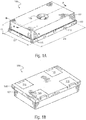
- FIG. 1A schematically shows a top perspective view of a top-ported MEMS microphone package 100.
- FIG. 1B schematically shows a bottom perspective view of the top-ported MEMS microphone package 100 shown in FIG. 1A .
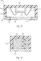
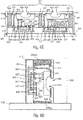
- FIGS. 1C , 1E, and 1F schematically show various examples of a cross-sectional view of the top-ported MEMS microphone package 100 of FIG. 1A across a line A-A.
- FIG. 1D provides another cross-sectional view of the top-ported MEMS microphone package 100 of FIG. 1A across a line B-B.
- the MEMS microphone package 100 may be used in any of a wide variety of applications.
- the MEMS microphone package 100 may be used with mobile telephones, land-line telephones, computer devices, video games, hearing aids, hearing instruments, biometric security systems, two-way radios, public announcement systems, and other devices that transduce signals.
- the MEMS microphone package 100 may have a first dimension D1 (e.g. a thickness) between about 0.9 mm and 2 mm, a second dimension D2 (e.g. a depth) between about 2 mm and 7 mm, and a third dimension D3 (e.g. a width) between about 3 mm and 10 mm.
- the MEMS microphone package 100 includes a lid component 101 and an acoustic input port 103 formed through the lid 101.
- the lid 101 may be an injection-molded thermoplastic component or a laminate substrate with integrated electronic circuit traces, as described in further detail below.
- the lid 101 is formed with a hollow cavity inside.
- the lid 101 is coupled to a substrate layer 105 to form a sealed cavity.
- the substrate layer 105 may be a laminate substrate including, for example, printed circuit board (PCB) material, such as FR-4.
- the substrate layer 105 may be a premolded leadframe-type package (also referred to as a "premolded package"). Further examples of the substrate layer 105 include ceramic cavity packages.
- a MEMS microphone die 107 is mounted to the lid 101 adjacent to or covering the acoustic port opening 103 such that acoustic pressures (e.g. sound waves) entering the MEMS microphone package 100 through the acoustic input port 103 engage or interact with the MEMS microphone die 107 to produce an electrical signal that, with additional (exterior and/or interior) components (e.g., a speaker and accompanying circuitry), produce an output audible signal corresponding to the input acoustic pressures.
- the MEMS microphone die 107 may be mounted to the lid 101 by an adhesive or another fastening mechanism known in the art.
- Conductive traces 109 are deposited on at least a portion of the interior surface of the lid 101.
- the conductive traces 109 are electrically coupled with corresponding traces 111 formed on the substrate layer 105.
- the circuit traces 111 on the substrate layer 105 are coupled to one or more conductive vias 113 which, in turn, are coupled to one or more electrical contact pads 115 on the bottom surface of the substrate layer 105.
- the electrical contact pads 115 are shown in greater detail in the bottom perspective view of FIG. 1B .
- the electrical contact pads 115 also referred to as package input/output (I/O) pads, electrically connect the MEMS microphone package 100 to another substrate, such as a main board, a printed circuit board, or other electrical interconnect apparatus.
- the electrical contact pads 115 may provide power and signal connections for the MEMS microphone package 100.
- FIG. 1D provides a more detail view of the interior surface of the lid 101 and represents the cross-sectional view of the top-ported MEMS microphone package 100 across line B-B of FIG. 1A .
- conductive traces 109 deposited on the interior walls of the lid 101 provide for electrical routing between the lid 101 and the substrate layer 105.
- interior surfaces of the lid 101 that are not used for electrical routing between the lid 101 and the substrate layer 105 are covered with a conductive layer 119 that is grounded to the substrate layer 105.
- the conductive layer 119 together with the substrate layer 105 (which may also include a conductive ground plate), forms a Faraday's cage that provides improved electromagnetic shielding of the MEMS microphone package 100.
- the conductive layer 119 may, additionally or alternatively, be positioned at or around the exterior surface of the lid 101, with the conductive layer 119 being coupled to the grounding of the substrate 105 to provide for electromagnetic shielding of the MEMS microphone package 100.
- the conductive layer 119 may be a single layer uniformly coating the lid 101 or may take the form of vias arranged along saw-streets of the lid 101.
- wires 117 extend from the MEMS microphone die 107 to couple the MEMS microphone die 107 to the conductive traces 109 formed on the interior surface of the lid 101.
- the MEMS microphone die 107 is in electronic communication with one or more devices mounted on the substrate layer 105 including, in this example, the electric contact pads 115 on the exterior surface of the MEMS microphone package 100.
- the MEMS microphone die 107 is a monolithically integrated MEMS die, which includes both application specific integrated circuit (ASIC) components and the micro-mechanical electric microphone diaphragm within a single die.
- ASIC application specific integrated circuit
- the micro-mechanical electric microphone diaphragm and the ASIC components may be provided as separate integrated circuits.
- the lid 101 is provided with both a MEMS microphone die 107' (that includes the micro-mechanical electric microphone diaphragm) and an ASIC 121.
- the MEMS microphone die 107' is mounted to the lid 101 adjacent to or over the acoustic input port 101, and the ASIC 121 is also mounted to the inner surface of the lid 101, adjacent to the MEMS microphone die 107'.
- the ASIC 121 may be covered by an encapsulation (e.g. glob top).
- the MEMS microphone die 107' and the ASIC 121 may be mounted to the lid 101 by an adhesive or another fastening mechanism.
- the wires 117 electrically connect the MEMS microphone die 107' and the ASIC 121 to each other and to the substrate layer 105 (and consequently the electrical contact pads 115) when the cavity is sealed.
- FIG. 1F is a cross-sectional view of another example of the top-ported MEMS microphone package 100 across line A-A of FIG. 1A .
- the lid 101 and the substrate layer 105 form the internal chamber for containing MEMS microphone die 107' and the ASIC 121 (which is used to control and drive the MEMS microphone die 107').
- the ASIC 121 and the MEMS microphone die 107' may be integrated within a single die (e.g. as in the example of FIG. 1C ).
- FIGS. 1A to 1F show examples of a top-ported MEMS microphone package 100
- some microphone packages position the acoustic input port 103 through the substrate layer 105 to form a bottom-ported MEMS microphone package 200, such as in the examples of FIGS. 2A to 2C .
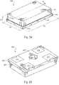
- FIG. 2A schematically shows a top perspective view of a bottom-ported MEMS microphone package 200.
- FIG. 2B schematically shows a bottom perspective view of the bottom-ported MEMS microphone package 200 shown in FIG. 2A .
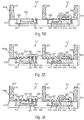
- FIG. 2C schematically shows a cross-sectional view of the bottom-ported MEMS microphone package 200 of FIG. 2A across a line C-C. As depicted in FIG.
- the MEMS microphone package 200 may have a first dimension D1 (e.g. a thickness), a second dimension D2 (e.g. a depth), and a third dimension D3, which may be similar to the first dimension D1, the second dimension D2, and the third dimension D3, respectively, of the MEMS microphone package 100 shown in FIG. 1A .
- a first dimension D1 e.g. a thickness
- a second dimension D2 e.g. a depth
- D3 which may be similar to the first dimension D1, the second dimension D2, and the third dimension D3, respectively, of the MEMS microphone package 100 shown in FIG. 1A .
- the MEMS microphone package 200 includes a lid component 201 as well as an acoustic input port 203 formed through a substrate layer 205.
- the lid 201 is coupled to (e.g. adhered to) the substrate layer 205 to form a sealed cavity.
- the substrate layer 205 may include similar materials as the substrate layer 105 described above in reference to FIGS. 1A to 1F . As illustrated in FIG.
- a MEMS microphone die 207' (including a micro-mechanical electric microphone diaphragm) is mounted to the substrate layer 205 adjacent to or covering the acoustic port opening 203 such that acoustic pressures (e.g., sound waves) entering the MEMS microphone package 200 through the acoustic input port 203 engage or interact with the MEMS microphone die 207 to produce an electrical signal that, with additional (exterior and/or interior) components (e.g., a speaker and accompanying circuitry), produce an output audible signal corresponding to the input acoustic pressures.
- the MEMS microphone die 207' may be mounted to the substrate layer 205 by an adhesive or another fastening mechanism known in the art.
- the lid 201 may be formed from one or more metals or another conductive material to shield the MEMS microphone die 207' from electromagnetic interference.
- Circuit traces 211 on the substrate layer 205 are coupled to one or more conductive vias 213 which, in turn, are coupled to one or more electrical contact pads 215 on the bottom surface of the substrate 205.
- the electrical contact pads 215 on the bottom surface of the substrate 205 are also shown in the bottom perspective view of FIG. 2B .
- the electrical contact pads 215 may electrically connect the MEMS microphone package 200 to another substrate, such as a main board, a printed circuit board, or other electrical interconnect apparatus.
- the electrical contact pads 215, also referred to as package input/output (I/O) pads, may provide power and signal connections for the MEMS microphone package 200.
- Wires 217 couple an ASIC 221 (which is used to control and drive the MEMS microphone die 207') and the MEMS microphone die 207' to each other. Wires 217 also serve to couple the ASIC 221 to the circuit traces 211 on the substrate 205.
- the ASIC 221 may be covered by an encapsulation (e.g. glob top).
- the ASIC 221 and the MEMS microphone die 207' may be provided as a monolithically integrated MEMS die (e.g. as in the example of FIG. 1A ).
- top-ported MEMS microphone packages and bottom-ported MEMS microphone packages require different bill of materials (BOMs) and process steps for their respective manufacture.
- BOMs bill of materials
- the top-ported MEMS microphone package 100 and the bottom-ported MEMS microphone package 200 have different manufacturing steps, raw materials, sub-assemblies, intermediate assemblies, sub-components, parts, and the quantities of each needed to manufacture the resultant MEMS microphone package.
- the top-ported MEMS microphone package 100 may require the use of two laminate substrates (e.g.
- a currently available MEMS microphone package is either top-ported or bottom-ported. In other words, the current market only offers single-package solutions that are either top-ported or bottom-ported.
- FIG. 3 shows a top-down view of a microphone array 300 including a main board 301 (e.g. a PCB) and a plurality of MEMS microphone packages 303 disposed on (e.g. mounted on and electrically coupled to) the main board 301.
- the microphone array 300 may be used, for example, in a smart consumer product and/or for at least one of voice recognition, command capturing and recognition, or noise suppression.
- the example of FIG. 3 illustrates a circular array of MEMS microphone packages 303; however, it is noted that other spatial arrangements of the MEMS microphone packages 303 may be possible (e.g. linear array or matrix).
- Respective ones of the plurality of MEMS microphone packages 303 may be identified with either the top-ported MEMS microphone package 100 of FIG. 1A or the bottom-ported MEMS microphone package 200 of FIG. 2A .
- the plurality of MEMS microphone packages 303 of the microphone array 300 may all be top-ported MEMS microphone packages or may all be bottom-ported MEMS microphone packages or may be a mixture thereof.
- the use of top-ported MEMS microphone packages and/or bottom-ported MEMS microphone packages (that have different BOMs) in the microphone array 300 can result in complexity in manufacturing and set up, which consequently could increase manufacturing costs. This is especially true in examples where the plurality of MEMS microphone packages 303 includes a mixture of top-ported MEMS microphone packages and bottom-ported MEMS microphone packages (e.g.
- the acoustic input port 103 of a top-ported MEMS microphone package may be directed away from a major surface 305 (e.g. top or upward-facing surface) of the main board 301, while the acoustic input port 203 of a bottom-ported MEMS microphone package may be directed towards the major surface 305 of the main board 301 (and may extend through a thickness of the main board 301). Consequently, the microphone array 300 of FIG. 3 may not be sufficiently sensitive to sound waves 307 that arrive laterally (e.g. sideways) at the plurality of MEMS microphone packages 303. Stated differently, the microphone array 300 of FIG.
- a current solution to this scenario is the use of additional features (e.g. sound guides) to channel the sound waves 307 to the top surface and/or the bottom surface of the main board 301 in an effort to guide the sound waves 307 into the top-facing or bottom-facing acoustic input ports 103, 203 of the plurality of MEMS microphone packages 303 so as to enable the plurality of MEMS microphone packages 303 to detect the sound waves 307.
- additional features e.g. sound guides
- the microphone array 300 generally occupies an area that may limit its implementation in mobile applications.
- an improved MEMS microphone package that: (1) is compact in size (e.g.
- FIGS. 4A to 4C and FIGS. 5A to 5F show a process flow illustrating a method of manufacturing a MEMS microphone package, in accordance with an embodiment.
- Example MEMS microphone packages that may be manufactured using the process flow of FIGS. 4A to 4C and FIGS. 5A to 5F are illustrated in FIGS. 7A, 7B , 8A, and 8B .
- the MEMS microphone packages may subsequently be used to conveniently and cheaply manufacture (in a modular manner and at the package-level) MEMS microphone arrays that are sensitive to sound waves travelling laterally.
- Example MEMS microphone arrays that may be manufactured using the MEMS microphone packages of FIGS. 7A, 7B , 8A, and 8B are shown in FIGS. 9A to 9E and 10A to 10E .
- FIG. 4A shows a frame 401 for a MEMS microphone package.
- the frame 401 includes portions that form one or more lids in an assembled MEMS microphone package (e.g. after singulation as described below).
- the frame 401 may have one or more ports 405 (e.g. that ultimately form acoustic input ports of the assembled MEMS microphone package) that extend through the frame 401.
- the frame 401 may also have bleed stop ridges 403 formed on one side of the frame 401.
- the bleed stop ridges 403 may be raised areas on the top surface of the frame 401, and each bleed stop ridge 403 may be formed to surround a respective port 405, and provide a physical barrier that prevents material applied to the top surface of the frame 401 from bleeding, or running outside of the bleed stop ridges 403.
- the frame 401 may be formed from a conductive material to provide electromagnetic interference (EMI) shielding for the assembled MEMS microphone package.
- the frame 401 may be made from copper, gold, aluminum, or another metal or alloy, and may be formed by molding, by chemical or plasma etching, by milling, by stamping, or by another formation process.
- the frame 401 may be made from a conductive material, such as a molding compound having conductive material disposed therein, or a conductive polymer such as an epoxy, molding compound, or the like.
- FIG. 4B illustrates mounting of MEMS microphone dies 407 on the frame 401 to form the first portion 413 of the MEMS microphone package according to some embodiments.
- An adhesive 411 such as glue, epoxy, die-attach film (DAF), or the like, is deposited on the top surface of the frame 401 within the bleed stop ridges 403, which contain the adhesive 411.
- the bleed stop ridges 403 prevent the adhesive 411 from flowing between areas designated for different lids or packages.
- MEMS microphone dies 407 are mounted on the adhesive 411 (that may be subsequently cured) so that the MEMS microphone dies 407 are affixed to the top surface of the frame 401.
- each of the MEMS microphone dies 407 may be attached to the frame 401 spanning a respective port 405.
- Each of the MEMS microphone dies 407 may have a sensor cavity 415 or the like that acts as a front chamber or front volume for the respective MEMS microphone die 407.
- FIG. 4C illustrates mounting of interconnects 421 and 423 on the first portion 413 of the shielded MEMS microphone package according to some embodiments.
- the interconnects 421 and 423 may include frame interconnects 423 that are mounted on and in electrical contact with the frame 401.
- the frame interconnects 423 are mounted on the bleed stop ridges 403, or on another exposed portion of the frame 401, and may provide a ground connection for the frame 401 or lids.
- the interconnects 421 and 423 may also include die interconnects 421 that are mounted on die landing pads 409 disposed on a top side of the MEMS microphone dies 407.
- the interconnects 421 and 423 may be wirebond structures that are formed using a wirebond machine that forms a ball at the end of an exposed wire using, for example, an electric flame-off, and may weld, fuse or otherwise attach the ball end of the interconnect to the bleed stop ridges 403 and die landing pads 409 using, for example, heat, pressure, and/or ultrasonic vibration. After the ball end of the wire is attached to the contact pad 115, the wirebonding machine may cut the wire to form a second end of the interconnects 421 and 423.
- the interconnects 421 and 423 have a first end disposed on the frame 401 or on the MEMS microphone die 407, and extend away from the frame 401.
- Second ends of the interconnects 421 and 423 are opposite the first ends of the interconnects 421 and 423.
- the second ends of the interconnects 421 and 423 are substantially level or coplanar to facilitate subsequent mounting of a substrate over the first portion 413.
- the interconnects 421 and 423 are solder balls, solder balls with supporting structures, preformed structures that are placed on the contact pad, printed structures or structures that are formed in place on the frame 401 or die landing pads 409.
- FIG. 5A shows a second portion 501 of the shielded MEMS microphone package, the second portion 501 having one or more pads 505 (e.g. landing pads) disposed at a major surface of a substrate 513 (e.g. a PCB).
- the one or more pads 505 may be interconnected by one or more metal lines and/or vias 507 on the substrate 513 or in a substrate body 503. It is noted that the one or more metal lines and/or vias 507 may be configured to provide power and signal connections for the assembled MEMS microphone package.
- FIG. 5B illustrates formation of sidewalls 509 on the second portion 501 according to some embodiments.
- the sidewalls 509 are formed on the substrate body 503, and in other embodiments, the sidewalls 509 may be formed on a stopper pad, oxide or sealing layer, or the like, that is disposed on a surface of the substrate 513.
- the sidewalls 509 are formed from a molding compound that is amenable to a plating process.
- the sidewalls 509 may include an elastomer molding compound material, and an outer surface 509a of the sidewalls 509 may subsequently be plated with a conductive material (e.g.
- the sidewall 509 may be formed by molding the sidewall in place, by 3D printing, by preforming the sidewall 509 and attaching the sidewall 509 to the substrate 513, or another forming process.
- the sidewall 509 is formed to contiguously surround a die area and one or more of the pads 505, and extend away from the substrate 513 to provide the interior cavities 511.
- FIG. 5C illustrates attachment of a control chip 515 according to some embodiments.
- the control chip 515 may be an ASIC, communications device, an interface device, or the like, and may have circuitry that controls, or reads the MEMS microphone die 407.
- the control chip 515 is attached to the substrate 513 by a die attachment structure 519 such as DAF, adhesive, tape, or the like.
- the control chip 515 is attached to the substrate 513 with a mechanical retainer such as a clip, socket, screw, or the like.
- the control chip 515 has one or more control chip bond pads 517 disposed on a top side that faces away from the substrate 513.
- FIG. 5D illustrates wirebonding of the control chip 515 to one or more pads 505 according to some embodiments.
- control chip 515 is a wirebonded control chip and is electrically connected to one or more of the pads 505 using wirebond connections 523. While FIGS. 5C and 5D illustrate that the control chip 515 may be wirebonded to the substrate 513, pad mounted control chips (such as in the example of FIG. 5E ) are also possible.
- FIG. 5E illustrates attachment of a pad mounted control chip 529 according to some embodiments.
- Conductive connectors 527 may be applied to one or more of the pads 505.
- a package includes a control chip 529 mounted by mounting pads 531 disposed on a bottom side of the control chip 529.
- the pad mounted control chip 529 is attached to pads 505 by the conductive connectors 527.
- the pad mounted control chip 529 may be an ASIC, communications device, an interface device, or the like, and may have circuitry that controls, or reads the MEMS microphone die 407. While the second portion 501 of the shielded sensor package illustrated in FIG.
- FIG. 5E illustrates application of a lid connector 537 to the sidewalls 509 according to some embodiments.
- the lid connector is disposed on second ends of the sidewalls 509, and may be a glue, DAF, epoxy, or another adhesive or attachment structure.
- FIGS. 6A to 6E illustrate assembly of shielded MEMS microphone packages 600, according to some embodiments.
- FIG. 6A illustrates attachment of the first portion 413 of FIG. 4C to the second portion 501 of FIG. 5F .
- the first portion 413 is inverted and affixed to the second portion 501 by the lid connectors 537 to enclose the interior cavity 511.
- the interconnects 421 and 423 are attached to the pads 505 of the second portion and affixed by the conductive connectors 527.
- the top surfaces of the pads 505 are substantially level so that the ends of the interconnects 421 and 423 make consistent contact with respective pads 505.
- each of the interconnects 421 and 423 extends from the first portion 413 of the shielded MEMS microphone package 600 so that a second end of each of the interconnects 421 and 423 is in electrical contact with a different contact pad 505 on the surface of the substrate 513.
- one or more of the interconnects 421 and 423 contacts a control chip bond pad 517, or another landing pad, contact pad, or the like.
- the MEMS microphone die 407 may be connected to a respective control chip 515 and 529 by way of the sensor interconnects 421 while the MEMS microphone die 407 and respective control chip 515 and 529 are spaced apart and overlapping each other.
- the spatial overlap of the MEMS microphone die 407 and the respective control chip 515 and 529 achieves a compact package footprint.
- one end of an interconnect 421 is attached to a die landing pad 409 of the MEMS microphone die 407, with the interconnect 421 extending away from the die landing pad 409.
- the other end of the interconnect 421 will then be in contact (e.g. electrical and/or physical contact) with the landing pad 505 on the substrate 531, with the landing pad 505 being electrically connected to the one or more metal lines and/or vias 507 disposed in the substrate body 503.
- the sidewalls 509 and frame 401 form a conductive shell providing EMI shielding for the enclosed control chips 515 and 529 and MEMS microphone dies 407.
- the substrate 513 also has a shielding layer (not shown), increasing the EMI shielding of the MEMS microphone packages 600.
- the interior cavity 511 acts as a back volume for the MEMS microphone dies 407, while the sensor cavity 415 acts as front volume.
- the packages 600 may be cured, reflowed, or the like to set, cure, or reflow the lid connectors 537 and conductive connectors 527.
- the MEMS microphone packages 600 may also be mounted on a carrier 539 such as a tape or the like.
- FIG. 6B illustrates singulation of the MEMS microphone packages 600 according to some embodiments.
- the MEMS microphone packages 600 are cut, for example, by die sawing, laser cutting, or the like, to form cut region 541 and separate the individual packages 600 while maintaining the MEMS microphone packages 600 on the carrier 539.
- FIG. 6B shows singulation to form individual packages 600, where each MEMS microphone package 600 includes a single MEMS microphone die 407
- the singulation process of FIG. 6B may be adapted or modified so that the structure of FIG. 6A is singulated to form individual packages 602 (e.g. a single package 602 shown in FIG. 6C ), where each MEMS microphone package 602 includes a plurality of MEMS microphone dies 407 (e.g. two MEMS microphone dies 407 in the example of FIG. 6C ).
- the sidewalls 509 may include an elastomer molding compound material, and the outer surface 509a of the sidewalls 509 may subsequently be plated with a conductive material (e.g. copper) to form electrical contact pads (also referred to as package input/output (I/O) pads) that provide power and signal connections for the MEMS microphone package 600 and that are electrically coupled to the one or more metal lines and/or vias 507 disposed in the substrate body 503.
- a conductive material e.g. copper
- electrical contact pads also referred to as package input/output (I/O) pads
- each singulated MEMS microphone package 600 may be picked from the carrier 539 and repositioned onto a carrier 539' such that a first outer surface 509a1 of the sidewalls 509 of each singulated MEMS microphone package 600 is in contact (e.g. physical contact) with and attached to the carrier 539', while a second outer surface 509a2 of the sidewalls 509 is upward-facing and directed away from the carrier 539'. Only one MEMS microphone package 600 is shown in FIG. 6D for the sake of simplicity.
- a plating and etching process known in the art may be carried out on the second outer surface 509a2 of the sidewalls 509 such that electrical contact pads 543 (also referred to as package input/output (I/O) pads) and traces 545 are formed at the second outer surface 509a2 of the sidewalls 509.
- the traces 545 are electrically and/or physically coupled to the electrical contact pads 543, with the traces 545 having terminal portions 545a that are formed at the surface 513a of the substrate 513 that is adjacent to the second outer surface 509a2 of the sidewalls 509. As illustrated in FIG.
- the traces 545 also extend into at least a portion of the substrate 513 so as to electrically couple the electrical contact pads 543 and the one or more metal lines and/or vias 507 to each other.
- an angle subtended between the portion of the trace 545 extending into the substrate 513 and the portion of the trace 545 disposed at the surface 513a of the substrate 513 may be about 90 degrees.
- Each singulated MEMS microphone package 600 may subsequently be removed from the carrier 539'.
- FIG. 7A schematically shows a top isometric view of the assembled MEMS microphone package 600 formed using the process shown in FIGS. 4A to 4C , FIGS. 5A to 5F , and 6A to 6E , according to some embodiments.
- FIG. 7B schematically shows a bottom isometric view of the MEMS microphone package 600 shown in FIG. 7A and illustrates, in greater detail, the electrical contact pads 543 and traces 545 formed at the bottom surface of the MEMS microphone package 600.
- FIG. 7C schematically shows a cross-sectional view of the MEMS microphone package of FIG. 7A along a line D-D.
- FIGS. 7A and 7B includes a single MEMS microphone that has a single acoustic input port 405 and lid 401 located at a first lateral side L1 (e.g. sidewall) of the MEMS microphone package 600.
- a second lateral side L2 of the MEMS microphone package 600 (opposite the first lateral side L1) may be formed by an exposed surface of the substrate 513.
- a third lateral side L3 and a fourth lateral side L4 of the MEMS microphone package 600 may be formed by the molding compound of sidewalls 509. Consequently, the MEMS microphone package 600 depicted in FIGS. 7A and 7B forms a single MEMS microphone having one side-port located on one side (e.g. lateral side Li) of the package 600.
- the MEMS microphone package 600 depicted in FIGS. 7A and 7B forms a single silicon microphone having one sound port located at one sidewall of the package 600.
- the MEMS microphone package 600 may have a first dimension D1 (e.g. a thickness) of about 2 mm, a second dimension D2 (e.g. a depth) of about 1 mm, and a third dimension D3 (e.g. a width) of about 2 mm, thus resulting in a compact package footprint (e.g. in comparison with the examples of FIGS. 1A and 2A ).
- the assembled MEMS microphone package 600 (and the method of its manufacture) achieves the following advantages: (1) being compact in size (e.g.
- having a small package footprint (2) having a standard BOM, while being easily configurable to be a top-ported MEMS microphone package, a bottom-ported MEMS microphone package, or a side-ported MEMS microphone package; and (3) being sensitive to sound waves travelling laterally (sideways) to the MEMS microphone package, without the use of additional features (e.g. sound guides).
- each MEMS microphone package 602 includes a plurality of MEMS microphone dies 407 (e.g. two MEMS microphone dies 407 in the example of FIG. 6C ).
- FIGS. 8A and 8B show such an example, where FIG. 8A schematically shows a top isometric view of the assembled MEMS microphone package 800 having two microphones and where FIG. 8B schematically shows a bottom isometric view of the MEMS microphone package 800 shown in FIG. 8A.
- FIG. 8B also illustrates, in greater detail, the electrical contact pads 543 and traces 545 formed at the bottom surface of the MEMS microphone package 800.
- the MEMS microphone package 800 of FIGS. 8A and 8B includes two MEMS microphones and two acoustic input ports 405 located at a first lateral side L1 of the MEMS microphone package 800.
- a third lateral side L3 and a fourth lateral side L4 of the MEMS microphone package 800 may be formed by the molding compound of sidewalls 509.
- a second lateral side L2 (which is opposite the first lateral side L1) of the MEMS microphone package 800 may be formed by an exposed surface of the substrate 513 (it is noted that a cross-sectional view along line E-E of FIG. 8A looks similar to FIG. 7C ). Consequently, the MEMS microphone package 800 depicted in FIGS.
- the MEMS microphone package 800 depicted in FIGS. 8A and 8B forms a microphone array having two MEMS microphones and two side-ports located on one side (e.g. lateral side Li) of the package 800.
- the MEMS microphone package 800 depicted in FIGS. 8A and 8B forms a microphone array (at the package level and not at the board level) having two sound ports located at one sidewall of the microphone package 800.
- the MEMS microphone package 800 may have a first dimension D1 (e.g. a thickness) of about 2 mm, a second dimension D2 (e.g. a depth) of about 1 mm, and a third dimension D3 (e.g. a width) of about 4 mm, thus resulting in a compact microphone array footprint (e.g.
- the assembled MEMS microphone package 800 (and the method of its manufacture) achieves the following advantages: (1) being compact in size (e.g. having a small package footprint); (2) having a standard BOM, while being easily configurable to be a top-ported MEMS microphone package, a bottom-ported MEMS microphone package, or a side-ported MEMS microphone package; (3) being modular in design so that it can easily be combined with other like MEMS microphone packages, at the package-level, to form a compact microphone array that may be suitable for mobile applications; and (4) being sensitive to sound waves travelling laterally (sideways) to the MEMS microphone package, without the use of additional features (e.g. sound guides).
- additional features e.g. sound guides
- FIGS. 9A and 9B schematically shows top isometric views of a MEMS microphone package 900 having two microphones;
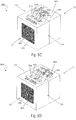
- FIGS. 9C and 9D schematically show bottom isometric views of the MEMS microphone package 900 shown in FIGS. 9A and 9B , respectively.
- FIG. 9E shows a cross-sectional view of the MEMS microphone package 900 across line F-F of FIG. 9A .
- the MEMS microphone package 900 may be formed by bonding (e.g. by an adhesive) the substrates 513 of two MEMS microphone packages 600 to each other, thereby forming a dual-side sound port microphone array.
- the resultant microphone array shown in FIGS. 9A to 9E has a stereo configuration.
- the MEMS microphone package 900 of FIGS. 9A to 9E includes one MEMS microphone and one acoustic input port 405 located at each of a first lateral side L1 and a second lateral side L2 of the MEMS microphone package 900.
- a third lateral side L3 and a fourth lateral side L4 of the MEMS microphone package 800 may be formed by the molding compound of sidewalls 509. Consequently, the MEMS microphone package 900 depicted in FIGS. 9A to 9E forms a microphone array having a first MEMS microphone and side-port 901 located opposite to a second MEMS microphone and side-port 903. Stated differently, the MEMS microphone package 900 depicted in FIGS.
- the MEMS microphone package 800 may have a first dimension D1 (e.g. a thickness) of about 2 mm, a second dimension D2 (e.g. a depth) of about 2.5 mm, and a third dimension D3 (e.g. a width) of about 2 mm, thus resulting in a compact microphone array footprint (e.g. in comparison with the example of FIG. 3 ).
- D1 e.g. a thickness
- D2 e.g. a depth
- D3 e.g. a width
- the assembled MEMS microphone package 900 achieves the following advantages: (1) being compact in size (e.g.
- having a small package footprint (2) having a standard BOM, while being easily configurable to be a top-ported MEMS microphone package, a bottom-ported MEMS microphone package, or a side-ported MEMS microphone package; (3) being modular in design so that it can easily be combined with other like MEMS microphone packages, at the package-level, to form a compact microphone array that may be suitable for mobile applications; and (4) being sensitive to sound waves travelling laterally (sideways) to the MEMS microphone package, without the use of additional features (e.g. sound guides).
- the MEMS microphone array 800 of FIGS. 8A and 8B may be combined with another MEMS microphone package 800 to form a dual-side sound port microphone array, as shown in FIGS. 10A to 10E .
- FIGS. 10A and 10B schematically shows top isometric views of a MEMS microphone package 1000 having four microphones;
- FIGS. 10C and 10D schematically show bottom isometric views of the MEMS microphone package 1000 shown in FIGS. 10A and 10B , respectively.
- FIG. 10E shows a cross-sectional view of the MEMS microphone package 1000 across line G-G of FIG. 10A .
- the MEMS microphone package 1000 may be formed by bonding (e.g. by an adhesive) the substrates 513 of two MEMS microphone packages 800 to each other, thereby forming a dual-side sound port microphone array.
- the resultant microphone array shown in FIGS. 10A to 10E has a stereo configuration.
- the MEMS microphone package 1000 of FIGS. 10A to 10E includes two MEMS microphone and two acoustic input ports 405 located at each of a first lateral side L1 and a second lateral side L2 of the MEMS microphone package 1000.
- a third lateral side L3 and a fourth lateral side L4 of the MEMS microphone package 1000 may be formed by the molding compound of sidewalls 509. Consequently, the MEMS microphone package 1000 depicted in FIGS. 10A to 10E forms a microphone array having a first MEMS microphone array 1001 located opposite to a second MEMS microphone array 1002. Stated differently, the MEMS microphone package 1000 depicted in FIGS.
- the MEMS microphone package 1000 may have a first dimension D1 (e.g. a thickness) of about 2 mm, a second dimension D2 (e.g. a depth) of about 2.5 mm, and a third dimension D3 (e.g. a width) of about 4 mm, thus resulting in a compact microphone array footprint (e.g. in comparison with the example of FIG. 3 ).
- D1 e.g. a thickness
- D2 e.g. a depth
- D3 e.g. a width
- the assembled MEMS microphone package 1000 (and the method of its manufacture) achieves the following advantages: (1) being compact in size (e.g. having a small package footprint); (2) having a standard BOM, while being easily configurable to be a top-ported MEMS microphone package, a bottom-ported MEMS microphone package, or a side-ported MEMS microphone package; (3) being modular in design so that it can easily be combined with other like MEMS microphone packages, at the package-level, to form a compact microphone array that may be suitable for mobile applications; and (4) being sensitive to sound waves travelling laterally (sideways) to the MEMS microphone package, without the use of additional features (e.g. sound guides).
- additional features e.g. sound guides
- a package and a method of manufacture thereof are provided.
- the proposed method results in a MEMS microphone package that is compact in size (e.g. having a small package footprint); has a standard BOM, while being easily configurable to be a top-ported MEMS microphone package, a bottom-ported MEMS microphone package, or a side-ported MEMS microphone package; is modular in design so that it can easily be combined with other like MEMS microphone packages, at the package-level, to form a compact microphone array that may be suitable for mobile applications; and is sensitive to sound waves travelling laterally (sideways) to the MEMS microphone package, without the use of additional features (e.g. sound guides).
- additional features e.g. sound guides
- the one or more lids of the assembled MEMS microphone package is formed by the frame 401, which can be envisioned as a flat metallic material that is attached or secured onto sidewalls 509, which include an encapsulation material such as a molding compound, a stopper pad, oxide or sealing layer.
- the proposed assembled MEMS microphone package can also be formed by a metal cap lid.
- FIG. 11 shows a cross-sectional view of an assembled MEMS microphone package 700 including a metal cap lid 701, in accordance with an embodiment. The example of FIG. 11 illustrates that the metal cap lid 701 is encapsulated by a molding compound 703.
- the metal cap lid 701 may be coupled (e.g. electrically and/or physically attached to) a contact pad 705 disposed on the substrate 513.
- the contact pad 705 may be electrically coupled to the traces 545 and/or metal lines 507 by a via 707.
- the MEMS microphone package 700 of FIG. 11 may be used to form the MEMS microphone packages/arrays shown in FIGS. 7A, 7B , 8A, 8B , 9A to 9D , and 10A to 10D .
- An embodiment device includes: a first sidewall including a first opening extending through the first sidewall; a first sensor attached to an interior surface of the first sidewall, wherein the first sensor is aligned to at least partially cover the first opening; a second sidewall opposite the first sidewall; a third sidewall attaching the first sidewall to the second sidewall; and a first contact pad disposed on an exterior surface of the third sidewall, wherein the first contact pad is configured to provide at least one of a power connection or a signal connection for the first sensor.
- An embodiment MEMS microphone package includes: a first lid forming a first sidewall of the MEMS microphone package, the first lid including a first acoustic input port extending through the first lid; a first MEMS microphone die attached to an interior surface of the first lid, where the first MEMS microphone die is aligned to at least partially cover the first acoustic input port; a second sidewall opposite the first lid; a molding compound forming a third sidewall and attaching the first lid to the second sidewall; and a first input/output (I/O) pad disposed on an exterior surface of the molding compound, where the first I/O pad is configured to provide at least one of a power connection or a signal connection for the first MEMS microphone die.
- I/O input/output
- An embodiment method includes: attaching a first side of a sensor to a first side of a lid, the sensor having a contact pad disposed on a second side of the sensor opposite the first side; providing an interconnect on the contact pad, where a first end of the interconnect is attached to the contact pad, and where the interconnect extends away from the contact pad; attaching a control chip to a first side of a substrate and electrically connecting the control chip to a first landing pad disposed at the first side of the substrate, the substrate further including a second landing pad disposed at the first side of the substrate and an interconnect structure disposed in a body of the substrate and electrically coupled to the second landing pad; affixing the lid over the substrate, where the affixing forms an interior cavity between the lid and the substrate that is bounded by a molding compound, and where the affixing causes a second end of the interconnect, opposite the first end of the interconnect, to be attached to the second landing pad; and forming an external contact pad and a trace on an exposed surface of the
- a device comprises: a first sidewall comprising a first opening extending through the first sidewall; a first sensor attached to an interior surface of the first sidewall, wherein the first sensor is aligned to at least partially cover the first opening; a second sidewall opposite the first sidewall; a third sidewall attaching the first sidewall to the second sidewall; and a first contact pad disposed on an exterior surface of the third sidewall, wherein the first contact pad is configured to provide at least one of a power connection or a signal connection for the first sensor.
- the first sensor comprises a first micro-electrical mechanical system (MEMS) microphone die.
- MEMS micro-electrical mechanical system
- the device further comprises a lid forming the first sidewall.
- the lid comprises a conductive material and provides electromagnetic interference (EMI) shielding for the first sensor.
- EMI electromagnetic interference
- the device further comprises a substrate, wherein the substrate comprises an interconnect structure disposed with a body of the substrate.
- the device further comprises a trace disposed on the exterior surface of the third sidewall and electrically coupling the interconnect structure and the first contact pad to each other, wherein a first end of the trace is coupled to the first contact pad and a second end of the trace is coupled to the interconnect structure.
- a first portion of the trace is disposed on the exterior surface of the third sidewall, a second portion of the trace extends through the substrate, and the first portion of the trace is perpendicular to the second portion of the trace.
- the substrate forms the second sidewall.
- the device further comprises a second opening and a second sensor aligned to at least partially cover the second opening.
- the second opening extends through the first sidewall and is adjacent to the first opening, and the second sensor is attached to the interior surface of the first sidewall.
- the device further comprises a third opening and a fourth opening extending through the second sidewall, wherein the third opening is adjacent to the fourth opening; and a third sensor and a fourth sensor aligned to at least partially cover the third opening and the fourth opening, respectively.
- the second opening extends through the second sidewall and is directed away from the first opening, and the second sensor is attached to an interior surface of the second sidewall.
- the device further comprises a second contact pad disposed on the exterior surface of the third sidewall, wherein the second contact pad is configured to provide at least one of a power connection or a signal connection for the second sensor.
- the device further comprises an interior cavity and a control chip disposed within the interior cavity, the control chip being configured to be in electrical communication with the first sensor.
- a MEMS microphone package comprises: a first lid forming a first sidewall of the MEMS microphone package, the first lid comprising a first acoustic input port extending through the first lid; a first MEMS microphone die attached to an interior surface of the first lid, wherein the first MEMS microphone die is aligned to at least partially cover the first acoustic input port; a second sidewall opposite the first lid; a molding compound forming a third sidewall and attaching the first lid to the second sidewall; and a first input/output (I/O) pad disposed on an exterior surface of the molding compound, wherein the first I/O pad is configured to provide at least one of a power connection or a signal connection for the first MEMS microphone die.
- I/O input/output
- the MEMS microphone package further comprises an interior cavity and an application specific integrated circuit (ASIC) die disposed within the interior cavity and electrically coupled to the first MEMS microphone die.
- ASIC application specific integrated circuit
- the first MEMS microphone die and the ASIC die spatially overlap at least partially.
- the MEMS microphone package further comprises a printed circuit board, wherein the printed circuit board comprises an interconnect structure disposed with a body of the printed circuit board.
- the MEMS microphone package further comprises a trace disposed on the exterior surface of the third sidewall and electrically coupling the interconnect structure and the first I/O pad to each other, wherein a first end of the trace is coupled to the first I/O pad and a second end of the trace is coupled to the interconnect structure, and wherein an angle subtended between the first end of the trace and the second end of the trace is substantially 90 degrees.
- an exterior surface of the printed circuit board forms an exterior surface of the second sidewall.
- the MEMS microphone package further comprises a second acoustic input port and a second MEMS microphone die aligned to at least partially cover the second acoustic input port.
- the second acoustic input port extends through the first lid and is adjacent to the first acoustic input port, and the second MEMS microphone die is attached to the interior surface of the first lid.
- the MEMS microphone package further comprises a second lid forming the second sidewall, wherein the second acoustic input port extends through the second lid and is directed away from the first acoustic input port, and wherein the second MEMS microphone die is attached to an interior surface of the second lid.
- the first lid and the second lid comprise a conductive material and provide electromagnetic interference (EMI) shielding for the first MEMS microphone die and the second MEMS microphone die, respectively.
- EMI electromagnetic interference
- a method comprises: attaching a first side of a sensor to a first side of a lid, the sensor having a contact pad disposed on a second side of the sensor opposite the first side; providing an interconnect on the contact pad, wherein a first end of the interconnect is attached to the contact pad, and wherein the interconnect extends away from the contact pad; attaching a control chip to a first side of a substrate and electrically connecting the control chip to a first landing pad disposed at the first side of the substrate, the substrate further comprising a second landing pad disposed at the first side of the substrate and an interconnect structure disposed in a body of the substrate and electrically coupled to the second landing pad; affixing the lid over the substrate, wherein the affixing forms an interior cavity between the lid and the substrate that is bounded by a molding compound, and wherein the affixing causes a second end of the interconnect, opposite the first end of the interconnect, to be attached to the second landing pad; and forming an external contact pad and
- the first end of the trace is perpendicular to the second end of the trace.
- forming the external contact pad and the trace on the exposed surface of the molding compound comprises a plating process.
- providing the interconnect comprises forming a wirebond interconnect with the first end of the interconnect as a ball end.
Landscapes
- Engineering & Computer Science (AREA)
- Microelectronics & Electronic Packaging (AREA)
- Manufacturing & Machinery (AREA)
- Physics & Mathematics (AREA)
- Signal Processing (AREA)
- Acoustics & Sound (AREA)
- Computer Hardware Design (AREA)
- Electromagnetism (AREA)
- Micromachines (AREA)
- Electrostatic, Electromagnetic, Magneto- Strictive, And Variable-Resistance Transducers (AREA)
- Details Of Audible-Bandwidth Transducers (AREA)
- Pressure Sensors (AREA)
- Testing Or Calibration Of Command Recording Devices (AREA)
Abstract
Description
- The present disclosure relates generally to sensors, and, in particular embodiments, to a micro-electrical mechanical system (MEMS) sensor package and a method of manufacture thereof.
- Generally, micro-electrical mechanical system (MEMS) sensor devices operate on physically sensible environmental conditions. For example, MEMS devices may sense sound, air pressure, motion, or the like. MEMS devices are generally simple sensor devices that generate a raw electrical signal. MEMS sensors, such as MEMS microphones, have a movable membrane that reacts to pressure waves in air in an interior cavity of the MEMS microphone to generate the electrical signal. A MEMS microphone package frequently includes a control chip, such as an application specific integrated circuit (ASIC), to manage the MEMS microphone, read the raw data signal from the MEMS microphone, and convert the data signal into a desired data format. In MEMS microphone package, the MEMS microphone and the control chip are disposed in a cavity of the device package.
- An embodiment device includes: a first sidewall including a first opening extending through the first sidewall; a first sensor attached to an interior surface of the first sidewall, wherein the first sensor is aligned to at least partially cover the first opening; a second sidewall opposite the first sidewall; a third sidewall attaching the first sidewall to the second sidewall; and a first contact pad disposed on an exterior surface of the third sidewall, wherein the first contact pad is configured to provide at least one of a power connection or a signal connection for the first sensor.
- An embodiment MEMS microphone package includes: a first lid forming a first sidewall of the MEMS microphone package, the first lid including a first acoustic input port extending through the first lid; a first MEMS microphone die attached to an interior surface of the first lid, where the first MEMS microphone die is aligned to at least partially cover the first acoustic input port; a second sidewall opposite the first lid; a molding compound forming a third sidewall and attaching the first lid to the second sidewall; and a first input/output (I/O) pad disposed on an exterior surface of the molding compound, where the first I/O pad is configured to provide at least one of a power connection or a signal connection for the first MEMS microphone die.
- An embodiment method includes: attaching a first side of a sensor to a first side of a lid, the sensor having a contact pad disposed on a second side of the sensor opposite the first side; providing an interconnect on the contact pad, where a first end of the interconnect is attached to the contact pad, and where the interconnect extends away from the contact pad; attaching a control chip to a first side of a substrate and electrically connecting the control chip to a first landing pad disposed at the first side of the substrate, the substrate further including a second landing pad disposed at the first side of the substrate and an interconnect structure disposed in a body of the substrate and electrically coupled to the second landing pad; affixing the lid over the substrate, where the affixing forms an interior cavity between the lid and the substrate that is bounded by a molding compound, and where the affixing causes a second end of the interconnect, opposite the first end of the interconnect, to be attached to the second landing pad; and forming an external contact pad and a trace on an exposed surface of the molding compound, where a first end of the trace is coupled to the external contact pad and a second end of the trace is coupled to the interconnect structure.
- For a more complete understanding of the present invention, and the advantages thereof, reference is now made to the following descriptions taken in conjunction with the accompanying drawings, in which:
-
FIG. 1A schematically shows a top perspective view of a top-ported MEMS microphone package; -
FIG. 1B schematically shows a bottom perspective view of the top-ported MEMS microphone package shown inFIG. 1A ; -
FIGS. 1C to 1F schematically show various cross-sectional views of the top-ported MEMS microphone package ofFIG. 1A ; -
FIG. 2A schematically shows a top perspective view of a bottom-ported MEMS microphone package; -
FIG. 2B schematically shows a bottom perspective view of the bottom-ported MEMS microphone package shown inFIG. 2A ; -
FIG. 2C schematically shows a cross-sectional view of the bottom-ported MEMS microphone package ofFIG. 2A ; -
FIG. 3 shows a top-down view of a microphone array including a main board and a plurality of MEMS microphone packages disposed on the main board; - FIGSS. 4A to 4C illustrate formation of a first portion of a MEMS microphone package, according to some embodiments;
-
FIGS. 5A to 5F illustrate formation of a second portion of a MEMS microphone package, according to some embodiments; -
FIGS. 6A to 6E illustrate assembly of a MEMS microphone package using the first portion obtained fromFIGS. 4A to 4C and the second portion obtained fromFIGS. 5A to 5F , according to some embodiments; -
FIGS. 7A and8A schematically show a top isometric view of a MEMS microphone package formed using the process shown inFIGS. 4A to 4C ,FIGS. 5A to 5F , and6A to 6E , according to some embodiments; -
FIGS. 7B and8B schematically show a bottom isometric view of the MEMS microphone package shown inFIG. 7A and8A , respectively, according to some embodiments; -
FIG. 7C schematically shows a cross-sectional view of the MEMS microphone package ofFIG. 7A , according to some embodiments; -
FIGS. 9A to 9E and10A to 10E schematically show various views of a MEMS microphone array, according to some embodiments; -
FIG. 11 shows a MEMS microphone package including a metal cap lid, according to some embodiments. - Corresponding numerals and symbols in different figures generally refer to corresponding parts unless otherwise indicated. The figures are drawn to clearly illustrate the relevant aspects of the preferred embodiments and are not necessarily drawn to scale. To more clearly illustrate certain embodiments, a letter indicating variations of the same structure, material, or process step may follow a figure number.
- The making and using of the presently preferred embodiments are discussed in detail below. It should be appreciated, however, that the present invention provides many applicable inventive concepts that can be embodied in a wide variety of specific contexts. The specific embodiments discussed are merely illustrative of specific ways to make and use the invention, and do not limit the scope of the invention.
- Reference may be made herein to the spatial relationships between various components and to the spatial orientation of various aspects of components as the devices are depicted in the attached drawings. However, as will be recognized by those skilled in the art after a complete reading of the present disclosure, the devices, members, apparatuses, etc. described herein may be positioned in any desired orientation. Thus, the use of terms such as "above," "below," "upper," "lower," or other like terms to describe a spatial relationship between various components or to describe the spatial orientation of aspects of such components should be understood to describe a relative relationship between the components or a spatial orientation of aspects of such components, respectively, as the device described herein may be oriented in any desired direction.
- The increasing complexity of electronic systems has given rise to requirements for ever increasing functionality in those electronic systems and decreasing size in the components used for the systems. In particular, personal electronic devices have an increasing number of microphones in order to detect sound in a variety of device orientations and additional sensors for new features. As the number of sensors increased, the space allocated to each sensor (and consequently to the microphones) decreases. Embodiments provide a MEMS microphone package and method of manufacture thereof that reduces package size and increases reliability and sensitivity. In particular, the disclosed embodiments are compact in size (e.g. having a small package footprint); have a standard bill of materials, while being easily configurable to be a top-ported MEMS microphone package, a bottom-ported MEMS microphone package, or a side-ported MEMS microphone package; are modular in design so that it can easily be combined with other like MEMS microphone packages, at the package-level, to form a compact microphone array that may be suitable for mobile applications; and are sensitive to sound waves travelling laterally (sideways) to the MEMS microphone package, without the use of additional features (e.g. sound guides).
-
FIG. 1A schematically shows a top perspective view of a top-portedMEMS microphone package 100.FIG. 1B schematically shows a bottom perspective view of the top-portedMEMS microphone package 100 shown inFIG. 1A .FIGS. 1C ,1E, and 1F schematically show various examples of a cross-sectional view of the top-portedMEMS microphone package 100 ofFIG. 1A across a line A-A.FIG. 1D provides another cross-sectional view of the top-portedMEMS microphone package 100 ofFIG. 1A across a line B-B. TheMEMS microphone package 100 may be used in any of a wide variety of applications. For example, theMEMS microphone package 100 may be used with mobile telephones, land-line telephones, computer devices, video games, hearing aids, hearing instruments, biometric security systems, two-way radios, public announcement systems, and other devices that transduce signals. TheMEMS microphone package 100 may have a first dimension D1 (e.g. a thickness) between about 0.9 mm and 2 mm, a second dimension D2 (e.g. a depth) between about 2 mm and 7 mm, and a third dimension D3 (e.g. a width) between about 3 mm and 10 mm. - Referring to
FIG. 1A , theMEMS microphone package 100 includes alid component 101 and anacoustic input port 103 formed through thelid 101. Thelid 101 may be an injection-molded thermoplastic component or a laminate substrate with integrated electronic circuit traces, as described in further detail below. As illustrated inFIG. 1C , thelid 101 is formed with a hollow cavity inside. Thelid 101 is coupled to asubstrate layer 105 to form a sealed cavity. Thesubstrate layer 105 may be a laminate substrate including, for example, printed circuit board (PCB) material, such as FR-4. In other examples, thesubstrate layer 105 may be a premolded leadframe-type package (also referred to as a "premolded package"). Further examples of thesubstrate layer 105 include ceramic cavity packages. - As illustrated in
FIG. 1C , a MEMS microphone die 107 is mounted to thelid 101 adjacent to or covering theacoustic port opening 103 such that acoustic pressures (e.g. sound waves) entering theMEMS microphone package 100 through theacoustic input port 103 engage or interact with the MEMS microphone die 107 to produce an electrical signal that, with additional (exterior and/or interior) components (e.g., a speaker and accompanying circuitry), produce an output audible signal corresponding to the input acoustic pressures. The MEMS microphone die 107 may be mounted to thelid 101 by an adhesive or another fastening mechanism known in the art. - Conductive traces 109 (e.g. metal traces) are deposited on at least a portion of the interior surface of the
lid 101. When thesubstrate layer 105 is sealed to the lid 101 (e.g. via a conductive or non-conductive sealant known in the art), theconductive traces 109 are electrically coupled withcorresponding traces 111 formed on thesubstrate layer 105. In the example ofFIG. 1C , the circuit traces 111 on thesubstrate layer 105 are coupled to one or moreconductive vias 113 which, in turn, are coupled to one or moreelectrical contact pads 115 on the bottom surface of thesubstrate layer 105. Theelectrical contact pads 115 are shown in greater detail in the bottom perspective view ofFIG. 1B . Theelectrical contact pads 115, also referred to as package input/output (I/O) pads, electrically connect theMEMS microphone package 100 to another substrate, such as a main board, a printed circuit board, or other electrical interconnect apparatus. Theelectrical contact pads 115 may provide power and signal connections for theMEMS microphone package 100. -
FIG. 1D provides a more detail view of the interior surface of thelid 101 and represents the cross-sectional view of the top-portedMEMS microphone package 100 across line B-B ofFIG. 1A . As noted above,conductive traces 109 deposited on the interior walls of thelid 101 provide for electrical routing between thelid 101 and thesubstrate layer 105. However, in this example, interior surfaces of thelid 101 that are not used for electrical routing between thelid 101 and thesubstrate layer 105 are covered with aconductive layer 119 that is grounded to thesubstrate layer 105. Theconductive layer 119, together with the substrate layer 105 (which may also include a conductive ground plate), forms a Faraday's cage that provides improved electromagnetic shielding of theMEMS microphone package 100. In some examples, theconductive layer 119 may, additionally or alternatively, be positioned at or around the exterior surface of thelid 101, with theconductive layer 119 being coupled to the grounding of thesubstrate 105 to provide for electromagnetic shielding of theMEMS microphone package 100. In such examples, theconductive layer 119 may be a single layer uniformly coating thelid 101 or may take the form of vias arranged along saw-streets of thelid 101. As shown inFIG. 1C ,wires 117 extend from the MEMS microphone die 107 to couple the MEMS microphone die 107 to the conductive traces 109 formed on the interior surface of thelid 101. As such, the MEMS microphone die 107 is in electronic communication with one or more devices mounted on thesubstrate layer 105 including, in this example, theelectric contact pads 115 on the exterior surface of theMEMS microphone package 100. - In the example of
FIG. 1C , the MEMS microphone die 107 is a monolithically integrated MEMS die, which includes both application specific integrated circuit (ASIC) components and the micro-mechanical electric microphone diaphragm within a single die. However, as shown in the example ofFIG. 1E , the micro-mechanical electric microphone diaphragm and the ASIC components may be provided as separate integrated circuits. For example, as illustrated inFIG. 1E , thelid 101 is provided with both a MEMS microphone die 107' (that includes the micro-mechanical electric microphone diaphragm) and anASIC 121. In other words, the MEMS microphone die 107' is mounted to thelid 101 adjacent to or over theacoustic input port 101, and theASIC 121 is also mounted to the inner surface of thelid 101, adjacent to the MEMS microphone die 107'. In some examples, theASIC 121 may be covered by an encapsulation (e.g. glob top). The MEMS microphone die 107' and theASIC 121 may be mounted to thelid 101 by an adhesive or another fastening mechanism. Thewires 117 electrically connect the MEMS microphone die 107' and theASIC 121 to each other and to the substrate layer 105 (and consequently the electrical contact pads 115) when the cavity is sealed. -
FIG. 1F is a cross-sectional view of another example of the top-portedMEMS microphone package 100 across line A-A ofFIG. 1A . Thelid 101 and thesubstrate layer 105 form the internal chamber for containing MEMS microphone die 107' and the ASIC 121 (which is used to control and drive the MEMS microphone die 107'). In other examples, theASIC 121 and the MEMS microphone die 107' may be integrated within a single die (e.g. as in the example ofFIG. 1C ). - While
FIGS. 1A to 1F show examples of a top-portedMEMS microphone package 100, some microphone packages position theacoustic input port 103 through thesubstrate layer 105 to form a bottom-portedMEMS microphone package 200, such as in the examples ofFIGS. 2A to 2C .FIG. 2A schematically shows a top perspective view of a bottom-portedMEMS microphone package 200. In a corresponding manner,FIG. 2B schematically shows a bottom perspective view of the bottom-portedMEMS microphone package 200 shown inFIG. 2A .FIG. 2C schematically shows a cross-sectional view of the bottom-portedMEMS microphone package 200 ofFIG. 2A across a line C-C. As depicted inFIG. 2A , theMEMS microphone package 200 may have a first dimension D1 (e.g. a thickness), a second dimension D2 (e.g. a depth), and a third dimension D3, which may be similar to the first dimension D1, the second dimension D2, and the third dimension D3, respectively, of theMEMS microphone package 100 shown inFIG. 1A . - Referring to
FIGS. 2A and 2B , theMEMS microphone package 200 includes alid component 201 as well as anacoustic input port 203 formed through asubstrate layer 205. Thelid 201 is coupled to (e.g. adhered to) thesubstrate layer 205 to form a sealed cavity. Thesubstrate layer 205 may include similar materials as thesubstrate layer 105 described above in reference toFIGS. 1A to 1F . As illustrated inFIG. 2C , a MEMS microphone die 207' (including a micro-mechanical electric microphone diaphragm) is mounted to thesubstrate layer 205 adjacent to or covering theacoustic port opening 203 such that acoustic pressures (e.g., sound waves) entering theMEMS microphone package 200 through theacoustic input port 203 engage or interact with the MEMS microphone die 207 to produce an electrical signal that, with additional (exterior and/or interior) components (e.g., a speaker and accompanying circuitry), produce an output audible signal corresponding to the input acoustic pressures. The MEMS microphone die 207' may be mounted to thesubstrate layer 205 by an adhesive or another fastening mechanism known in the art. Thelid 201 may be formed from one or more metals or another conductive material to shield the MEMS microphone die 207' from electromagnetic interference. - Circuit traces 211 on the
substrate layer 205 are coupled to one or moreconductive vias 213 which, in turn, are coupled to one or moreelectrical contact pads 215 on the bottom surface of thesubstrate 205. Theelectrical contact pads 215 on the bottom surface of thesubstrate 205 are also shown in the bottom perspective view ofFIG. 2B . Theelectrical contact pads 215 may electrically connect theMEMS microphone package 200 to another substrate, such as a main board, a printed circuit board, or other electrical interconnect apparatus. Theelectrical contact pads 215, also referred to as package input/output (I/O) pads, may provide power and signal connections for theMEMS microphone package 200.Wires 217 couple an ASIC 221 (which is used to control and drive the MEMS microphone die 207') and the MEMS microphone die 207' to each other.Wires 217 also serve to couple theASIC 221 to the circuit traces 211 on thesubstrate 205. In some examples, theASIC 221 may be covered by an encapsulation (e.g. glob top). In other examples, theASIC 221 and the MEMS microphone die 207' may be provided as a monolithically integrated MEMS die (e.g. as in the example ofFIG. 1A ). - It can be appreciated, from the general structure of the MEMS microphone packages 100 and 200 described above in reference to
FIGS. 1A to 1F and2A to 2C , that top-ported MEMS microphone packages and bottom-ported MEMS microphone packages require different bill of materials (BOMs) and process steps for their respective manufacture. In other words, the top-portedMEMS microphone package 100 and the bottom-portedMEMS microphone package 200 have different manufacturing steps, raw materials, sub-assemblies, intermediate assemblies, sub-components, parts, and the quantities of each needed to manufacture the resultant MEMS microphone package. For example, the top-portedMEMS microphone package 100 may require the use of two laminate substrates (e.g. one laminate substrate forsubstrate layer 105 and another laminate substrate for lid 101), while the bottom-portedMEMS microphone package 200 may require the use of one laminate substrate (e.g. for substrate layer 205) and onemetal lid 201. Furthermore, a currently available MEMS microphone package is either top-ported or bottom-ported. In other words, the current market only offers single-package solutions that are either top-ported or bottom-ported. - The currently available single-package solutions can complicate the manufacture of microphone arrays.
FIG. 3 shows a top-down view of amicrophone array 300 including a main board 301 (e.g. a PCB) and a plurality of MEMS microphone packages 303 disposed on (e.g. mounted on and electrically coupled to) themain board 301. Themicrophone array 300 may be used, for example, in a smart consumer product and/or for at least one of voice recognition, command capturing and recognition, or noise suppression. The example ofFIG. 3 illustrates a circular array of MEMS microphone packages 303; however, it is noted that other spatial arrangements of the MEMS microphone packages 303 may be possible (e.g. linear array or matrix). Respective ones of the plurality of MEMS microphone packages 303 may be identified with either the top-portedMEMS microphone package 100 ofFIG. 1A or the bottom-portedMEMS microphone package 200 ofFIG. 2A . Stated differently, the plurality of MEMS microphone packages 303 of themicrophone array 300 may all be top-ported MEMS microphone packages or may all be bottom-ported MEMS microphone packages or may be a mixture thereof. The use of top-ported MEMS microphone packages and/or bottom-ported MEMS microphone packages (that have different BOMs) in themicrophone array 300 can result in complexity in manufacturing and set up, which consequently could increase manufacturing costs. This is especially true in examples where the plurality of MEMS microphone packages 303 includes a mixture of top-ported MEMS microphone packages and bottom-ported MEMS microphone packages (e.g. since different BOMs are required). Additionally, since the plurality of MEMS microphone packages 303 are mounted on themain board 301, theacoustic input port 103 of a top-ported MEMS microphone package may be directed away from a major surface 305 (e.g. top or upward-facing surface) of themain board 301, while theacoustic input port 203 of a bottom-ported MEMS microphone package may be directed towards themajor surface 305 of the main board 301 (and may extend through a thickness of the main board 301). Consequently, themicrophone array 300 ofFIG. 3 may not be sufficiently sensitive tosound waves 307 that arrive laterally (e.g. sideways) at the plurality of MEMS microphone packages 303. Stated differently, themicrophone array 300 ofFIG. 3 may not adequately capturesound waves 307 that are incident on a sidewall of thelids sound waves 307 to the top surface and/or the bottom surface of themain board 301 in an effort to guide thesound waves 307 into the top-facing or bottom-facingacoustic input ports sound waves 307. However, such a solution further increases the costs and complexity associated with manufacturing themicrophone array 300. Even further, since themicrophone array 300 is generally produced at the board-level (e.g. by mounting the plurality of MEMS microphone packages 303 on the main board 301) and not at the package-level, themicrophone array 300 generally occupies an area that may limit its implementation in mobile applications. In view of these observations, there may be a need for an improved MEMS microphone package that: (1) is compact in size (e.g. having a small package footprint); (2) has a standard BOM, while being easily configurable to be a top-ported MEMS microphone package, a bottom-ported MEMS microphone package, or a side-ported MEMS microphone package; (3) is modular in design so that it can easily be combined with other like MEMS microphone packages, at the package-level, to form a compact microphone array that may be suitable for mobile applications; and (4) is sensitive to sound waves travelling laterally (sideways) to the MEMS microphone package, without the use of additional features (e.g. sound guides). -
FIGS. 4A to 4C andFIGS. 5A to 5F show a process flow illustrating a method of manufacturing a MEMS microphone package, in accordance with an embodiment. Example MEMS microphone packages that may be manufactured using the process flow ofFIGS. 4A to 4C andFIGS. 5A to 5F are illustrated inFIGS. 7A, 7B ,8A, and 8B . The MEMS microphone packages may subsequently be used to conveniently and cheaply manufacture (in a modular manner and at the package-level) MEMS microphone arrays that are sensitive to sound waves travelling laterally. Example MEMS microphone arrays that may be manufactured using the MEMS microphone packages ofFIGS. 7A, 7B ,8A, and 8B are shown inFIGS. 9A to 9E and10A to 10E . - Referring first to
FIGS. 4A to 4C , which illustrate formation of afirst portion 413 of a MEMS microphone package according to some embodiments,FIG. 4A shows aframe 401 for a MEMS microphone package. Theframe 401 includes portions that form one or more lids in an assembled MEMS microphone package (e.g. after singulation as described below). Theframe 401 may have one or more ports 405 (e.g. that ultimately form acoustic input ports of the assembled MEMS microphone package) that extend through theframe 401. Theframe 401 may also have bleed stopridges 403 formed on one side of theframe 401. The bleed stopridges 403 may be raised areas on the top surface of theframe 401, and each bleedstop ridge 403 may be formed to surround arespective port 405, and provide a physical barrier that prevents material applied to the top surface of theframe 401 from bleeding, or running outside of the bleed stopridges 403. - In some embodiments, the
frame 401 may be formed from a conductive material to provide electromagnetic interference (EMI) shielding for the assembled MEMS microphone package. In some embodiments, theframe 401 may be made from copper, gold, aluminum, or another metal or alloy, and may be formed by molding, by chemical or plasma etching, by milling, by stamping, or by another formation process. In other embodiments, theframe 401 may be made from a conductive material, such as a molding compound having conductive material disposed therein, or a conductive polymer such as an epoxy, molding compound, or the like. -
FIG. 4B illustrates mounting of MEMS microphone dies 407 on theframe 401 to form thefirst portion 413 of the MEMS microphone package according to some embodiments. An adhesive 411 such as glue, epoxy, die-attach film (DAF), or the like, is deposited on the top surface of theframe 401 within the bleed stopridges 403, which contain the adhesive 411. The bleed stopridges 403 prevent the adhesive 411 from flowing between areas designated for different lids or packages. In some embodiments, MEMS microphone dies 407 are mounted on the adhesive 411 (that may be subsequently cured) so that the MEMS microphone dies 407 are affixed to the top surface of theframe 401. In some embodiments, each of the MEMS microphone dies 407 may be attached to theframe 401 spanning arespective port 405. Each of the MEMS microphone dies 407 may have asensor cavity 415 or the like that acts as a front chamber or front volume for the respective MEMS microphone die 407. -
FIG. 4C illustrates mounting ofinterconnects first portion 413 of the shielded MEMS microphone package according to some embodiments. Theinterconnects frame 401. In some embodiments, the frame interconnects 423 are mounted on the bleed stopridges 403, or on another exposed portion of theframe 401, and may provide a ground connection for theframe 401 or lids. Theinterconnects interconnects 421 that are mounted ondie landing pads 409 disposed on a top side of the MEMS microphone dies 407. Theinterconnects ridges 403 and dielanding pads 409 using, for example, heat, pressure, and/or ultrasonic vibration. After the ball end of the wire is attached to thecontact pad 115, the wirebonding machine may cut the wire to form a second end of theinterconnects interconnects frame 401 or on the MEMS microphone die 407, and extend away from theframe 401. Second ends of theinterconnects interconnects interconnects first portion 413. In other embodiments, theinterconnects frame 401 or dielanding pads 409. - Referring now to
FIGS. 5A to 5F , which illustrate the formation of a second portion of the MEMS microphone package according to some embodiments.FIG. 5A shows asecond portion 501 of the shielded MEMS microphone package, thesecond portion 501 having one or more pads 505 (e.g. landing pads) disposed at a major surface of a substrate 513 (e.g. a PCB). The one ormore pads 505 may be interconnected by one or more metal lines and/orvias 507 on thesubstrate 513 or in asubstrate body 503. It is noted that the one or more metal lines and/orvias 507 may be configured to provide power and signal connections for the assembled MEMS microphone package. -
FIG. 5B illustrates formation ofsidewalls 509 on thesecond portion 501 according to some embodiments. In some embodiments, thesidewalls 509 are formed on thesubstrate body 503, and in other embodiments, thesidewalls 509 may be formed on a stopper pad, oxide or sealing layer, or the like, that is disposed on a surface of thesubstrate 513. In some embodiments, thesidewalls 509 are formed from a molding compound that is amenable to a plating process. For example, thesidewalls 509 may include an elastomer molding compound material, and anouter surface 509a of thesidewalls 509 may subsequently be plated with a conductive material (e.g. copper) to form electrical contact pads (also referred to as package input/output (I/O) pads) that provide power and signal connections for the assembled MEMS microphone package and that are electrically coupled to the one or more metal lines and/orvias 507 disposed in thesubstrate body 503. This step is described in greater detail inFIGS. 6D and6E . Thesidewall 509 may be formed by molding the sidewall in place, by 3D printing, by preforming thesidewall 509 and attaching thesidewall 509 to thesubstrate 513, or another forming process. Thesidewall 509 is formed to contiguously surround a die area and one or more of thepads 505, and extend away from thesubstrate 513 to provide theinterior cavities 511. -
FIG. 5C illustrates attachment of acontrol chip 515 according to some embodiments. Thecontrol chip 515 may be an ASIC, communications device, an interface device, or the like, and may have circuitry that controls, or reads the MEMS microphone die 407. Thecontrol chip 515 is attached to thesubstrate 513 by adie attachment structure 519 such as DAF, adhesive, tape, or the like. In other embodiments, thecontrol chip 515 is attached to thesubstrate 513 with a mechanical retainer such as a clip, socket, screw, or the like. Thecontrol chip 515 has one or more controlchip bond pads 517 disposed on a top side that faces away from thesubstrate 513.FIG. 5D illustrates wirebonding of thecontrol chip 515 to one ormore pads 505 according to some embodiments. In some embodiments, thecontrol chip 515 is a wirebonded control chip and is electrically connected to one or more of thepads 505 usingwirebond connections 523. WhileFIGS. 5C and5D illustrate that thecontrol chip 515 may be wirebonded to thesubstrate 513, pad mounted control chips (such as in the example ofFIG. 5E ) are also possible. -
FIG. 5E illustrates attachment of a pad mountedcontrol chip 529 according to some embodiments.Conductive connectors 527 may be applied to one or more of thepads 505. In some embodiments, a package includes acontrol chip 529 mounted by mountingpads 531 disposed on a bottom side of thecontrol chip 529. The pad mountedcontrol chip 529 is attached topads 505 by theconductive connectors 527. The pad mountedcontrol chip 529 may be an ASIC, communications device, an interface device, or the like, and may have circuitry that controls, or reads the MEMS microphone die 407. While thesecond portion 501 of the shielded sensor package illustrated inFIG. 5E is shown with awirebonded control chip 515 and a pad mountedcontrol chip 529, the different types ofcontrol chips FIG. 5F illustrates application of alid connector 537 to thesidewalls 509 according to some embodiments. The lid connector is disposed on second ends of thesidewalls 509, and may be a glue, DAF, epoxy, or another adhesive or attachment structure. -
FIGS. 6A to 6E illustrate assembly of shielded MEMS microphone packages 600, according to some embodiments.FIG. 6A illustrates attachment of thefirst portion 413 ofFIG. 4C to thesecond portion 501 ofFIG. 5F . Thefirst portion 413 is inverted and affixed to thesecond portion 501 by thelid connectors 537 to enclose theinterior cavity 511. Additionally, theinterconnects pads 505 of the second portion and affixed by theconductive connectors 527. In some embodiments, the top surfaces of thepads 505 are substantially level so that the ends of theinterconnects respective pads 505. In some embodiments, each of theinterconnects first portion 413 of the shieldedMEMS microphone package 600 so that a second end of each of theinterconnects different contact pad 505 on the surface of thesubstrate 513. In other embodiments, one or more of theinterconnects chip bond pad 517, or another landing pad, contact pad, or the like. Thus, the MEMS microphone die 407 may be connected to arespective control chip respective control chip respective control chip FIG. 6A and with respect tointerconnects 421, one end of aninterconnect 421 is attached to adie landing pad 409 of the MEMS microphone die 407, with theinterconnect 421 extending away from thedie landing pad 409. The other end of theinterconnect 421 will then be in contact (e.g. electrical and/or physical contact) with thelanding pad 505 on thesubstrate 531, with thelanding pad 505 being electrically connected to the one or more metal lines and/orvias 507 disposed in thesubstrate body 503. - The
sidewalls 509 andframe 401 form a conductive shell providing EMI shielding for theenclosed control chips substrate 513 also has a shielding layer (not shown), increasing the EMI shielding of the MEMS microphone packages 600. Additionally, in the arrangement illustrated, theinterior cavity 511 acts as a back volume for the MEMS microphone dies 407, while thesensor cavity 415 acts as front volume. After thefirst portion 413 is mounted on thesecond portion 501, thepackages 600 may be cured, reflowed, or the like to set, cure, or reflow thelid connectors 537 andconductive connectors 527. The MEMS microphone packages 600 may also be mounted on acarrier 539 such as a tape or the like. -
FIG. 6B illustrates singulation of the MEMS microphone packages 600 according to some embodiments. The MEMS microphone packages 600 are cut, for example, by die sawing, laser cutting, or the like, to form cutregion 541 and separate theindividual packages 600 while maintaining the MEMS microphone packages 600 on thecarrier 539. It is noted that while the example ofFIG. 6B shows singulation to formindividual packages 600, where eachMEMS microphone package 600 includes a single MEMS microphone die 407, the singulation process ofFIG. 6B may be adapted or modified so that the structure ofFIG. 6A is singulated to form individual packages 602 (e.g. asingle package 602 shown inFIG. 6C ), where eachMEMS microphone package 602 includes a plurality of MEMS microphone dies 407 (e.g. two MEMS microphone dies 407 in the example ofFIG. 6C ). - As discussed above in reference to
FIG. 5B , thesidewalls 509 may include an elastomer molding compound material, and theouter surface 509a of thesidewalls 509 may subsequently be plated with a conductive material (e.g. copper) to form electrical contact pads (also referred to as package input/output (I/O) pads) that provide power and signal connections for theMEMS microphone package 600 and that are electrically coupled to the one or more metal lines and/orvias 507 disposed in thesubstrate body 503. As shown inFIG. 6D , each singulatedMEMS microphone package 600 ofFIG. 6B may be picked from thecarrier 539 and repositioned onto a carrier 539' such that a first outer surface 509a1 of thesidewalls 509 of each singulatedMEMS microphone package 600 is in contact (e.g. physical contact) with and attached to the carrier 539', while a second outer surface 509a2 of thesidewalls 509 is upward-facing and directed away from the carrier 539'. Only oneMEMS microphone package 600 is shown inFIG. 6D for the sake of simplicity. - As shown in
FIG. 6E , a plating and etching process known in the art may be carried out on the second outer surface 509a2 of thesidewalls 509 such that electrical contact pads 543 (also referred to as package input/output (I/O) pads) and traces 545 are formed at the second outer surface 509a2 of thesidewalls 509. Thetraces 545 are electrically and/or physically coupled to theelectrical contact pads 543, with thetraces 545 havingterminal portions 545a that are formed at thesurface 513a of thesubstrate 513 that is adjacent to the second outer surface 509a2 of thesidewalls 509. As illustrated inFIG. 6E , thetraces 545 also extend into at least a portion of thesubstrate 513 so as to electrically couple theelectrical contact pads 543 and the one or more metal lines and/orvias 507 to each other. In some embodiments, an angle subtended between the portion of thetrace 545 extending into thesubstrate 513 and the portion of thetrace 545 disposed at thesurface 513a of thesubstrate 513 may be about 90 degrees. Each singulatedMEMS microphone package 600 may subsequently be removed from the carrier 539'. -
FIG. 7A schematically shows a top isometric view of the assembledMEMS microphone package 600 formed using the process shown inFIGS. 4A to 4C ,FIGS. 5A to 5F , and6A to 6E , according to some embodiments.FIG. 7B schematically shows a bottom isometric view of theMEMS microphone package 600 shown inFIG. 7A and illustrates, in greater detail, theelectrical contact pads 543 and traces 545 formed at the bottom surface of theMEMS microphone package 600.FIG. 7C schematically shows a cross-sectional view of the MEMS microphone package ofFIG. 7A along a line D-D. TheMEMS microphone package 600 ofFIGS. 7A to 7C includes a single MEMS microphone that has a singleacoustic input port 405 andlid 401 located at a first lateral side L1 (e.g. sidewall) of theMEMS microphone package 600. A second lateral side L2 of the MEMS microphone package 600 (opposite the first lateral side L1) may be formed by an exposed surface of thesubstrate 513. A third lateral side L3 and a fourth lateral side L4 of theMEMS microphone package 600 may be formed by the molding compound ofsidewalls 509. Consequently, theMEMS microphone package 600 depicted inFIGS. 7A and 7B forms a single MEMS microphone having one side-port located on one side (e.g. lateral side Li) of thepackage 600. Stated differently, theMEMS microphone package 600 depicted inFIGS. 7A and 7B forms a single silicon microphone having one sound port located at one sidewall of thepackage 600. As illustrated inFIG. 7A , theMEMS microphone package 600 may have a first dimension D1 (e.g. a thickness) of about 2 mm, a second dimension D2 (e.g. a depth) of about 1 mm, and a third dimension D3 (e.g. a width) of about 2 mm, thus resulting in a compact package footprint (e.g. in comparison with the examples ofFIGS. 1A and2A ). As such, the assembled MEMS microphone package 600 (and the method of its manufacture) achieves the following advantages: (1) being compact in size (e.g. having a small package footprint); (2) having a standard BOM, while being easily configurable to be a top-ported MEMS microphone package, a bottom-ported MEMS microphone package, or a side-ported MEMS microphone package; and (3) being sensitive to sound waves travelling laterally (sideways) to the MEMS microphone package, without the use of additional features (e.g. sound guides). - As discussed above, the singulation process of
FIG. 6B may be adapted or modified so that the structure ofFIG. 6A is singulated to form individual packages 602 (e.g.single package 602 shown inFIG. 6C ), where eachMEMS microphone package 602 includes a plurality of MEMS microphone dies 407 (e.g. two MEMS microphone dies 407 in the example ofFIG. 6C ).FIGS. 8A and 8B show such an example, whereFIG. 8A schematically shows a top isometric view of the assembledMEMS microphone package 800 having two microphones and whereFIG. 8B schematically shows a bottom isometric view of theMEMS microphone package 800 shown inFIG. 8A. FIG. 8B also illustrates, in greater detail, theelectrical contact pads 543 and traces 545 formed at the bottom surface of theMEMS microphone package 800. - The
MEMS microphone package 800 ofFIGS. 8A and 8B includes two MEMS microphones and twoacoustic input ports 405 located at a first lateral side L1 of theMEMS microphone package 800. A third lateral side L3 and a fourth lateral side L4 of theMEMS microphone package 800 may be formed by the molding compound ofsidewalls 509. A second lateral side L2 (which is opposite the first lateral side L1) of theMEMS microphone package 800 may be formed by an exposed surface of the substrate 513 (it is noted that a cross-sectional view along line E-E ofFIG. 8A looks similar toFIG. 7C ). Consequently, theMEMS microphone package 800 depicted inFIGS. 8A and 8B forms a microphone array having two MEMS microphones and two side-ports located on one side (e.g. lateral side Li) of thepackage 800. Stated differently, theMEMS microphone package 800 depicted inFIGS. 8A and 8B forms a microphone array (at the package level and not at the board level) having two sound ports located at one sidewall of themicrophone package 800. As illustrated inFIG. 8A , theMEMS microphone package 800 may have a first dimension D1 (e.g. a thickness) of about 2 mm, a second dimension D2 (e.g. a depth) of about 1 mm, and a third dimension D3 (e.g. a width) of about 4 mm, thus resulting in a compact microphone array footprint (e.g. in comparison with the example ofFIG. 3 ). As such, the assembled MEMS microphone package 800 (and the method of its manufacture) achieves the following advantages: (1) being compact in size (e.g. having a small package footprint); (2) having a standard BOM, while being easily configurable to be a top-ported MEMS microphone package, a bottom-ported MEMS microphone package, or a side-ported MEMS microphone package; (3) being modular in design so that it can easily be combined with other like MEMS microphone packages, at the package-level, to form a compact microphone array that may be suitable for mobile applications; and (4) being sensitive to sound waves travelling laterally (sideways) to the MEMS microphone package, without the use of additional features (e.g. sound guides). - The single
MEMS microphone package 600 ofFIGS. 7A and 7B may be combined with anotherMEMS microphone package 600 to form a dual-side sound port microphone array, as shown inFIGS. 9A to 9E .FIGS. 9A and 9B schematically shows top isometric views of aMEMS microphone package 900 having two microphones;FIGS. 9C and 9D schematically show bottom isometric views of theMEMS microphone package 900 shown inFIGS. 9A and 9B , respectively. Additionally,FIG. 9E shows a cross-sectional view of theMEMS microphone package 900 across line F-F ofFIG. 9A . As shown inFIG. 9E , theMEMS microphone package 900 may be formed by bonding (e.g. by an adhesive) thesubstrates 513 of two MEMS microphone packages 600 to each other, thereby forming a dual-side sound port microphone array. In other words, the resultant microphone array shown inFIGS. 9A to 9E has a stereo configuration. - The
MEMS microphone package 900 ofFIGS. 9A to 9E includes one MEMS microphone and oneacoustic input port 405 located at each of a first lateral side L1 and a second lateral side L2 of theMEMS microphone package 900. A third lateral side L3 and a fourth lateral side L4 of theMEMS microphone package 800 may be formed by the molding compound ofsidewalls 509. Consequently, theMEMS microphone package 900 depicted inFIGS. 9A to 9E forms a microphone array having a first MEMS microphone and side-port 901 located opposite to a second MEMS microphone and side-port 903. Stated differently, theMEMS microphone package 900 depicted inFIGS. 9A to 9E forms a microphone array (at the package level and not at the board level) having twosound ports 405 located at opposite sides of thepackage 900 in relation to each other. As illustrated inFIG. 9A , theMEMS microphone package 800 may have a first dimension D1 (e.g. a thickness) of about 2 mm, a second dimension D2 (e.g. a depth) of about 2.5 mm, and a third dimension D3 (e.g. a width) of about 2 mm, thus resulting in a compact microphone array footprint (e.g. in comparison with the example ofFIG. 3 ). As such, the assembled MEMS microphone package 900 (and the method of its manufacture) achieves the following advantages: (1) being compact in size (e.g. having a small package footprint); (2) having a standard BOM, while being easily configurable to be a top-ported MEMS microphone package, a bottom-ported MEMS microphone package, or a side-ported MEMS microphone package; (3) being modular in design so that it can easily be combined with other like MEMS microphone packages, at the package-level, to form a compact microphone array that may be suitable for mobile applications; and (4) being sensitive to sound waves travelling laterally (sideways) to the MEMS microphone package, without the use of additional features (e.g. sound guides). - The
MEMS microphone array 800 ofFIGS. 8A and 8B may be combined with anotherMEMS microphone package 800 to form a dual-side sound port microphone array, as shown inFIGS. 10A to 10E .FIGS. 10A and 10B schematically shows top isometric views of aMEMS microphone package 1000 having four microphones;FIGS. 10C and 10D schematically show bottom isometric views of theMEMS microphone package 1000 shown inFIGS. 10A and 10B , respectively. Additionally,FIG. 10E shows a cross-sectional view of theMEMS microphone package 1000 across line G-G ofFIG. 10A . As shown inFIG. 10E , theMEMS microphone package 1000 may be formed by bonding (e.g. by an adhesive) thesubstrates 513 of two MEMS microphone packages 800 to each other, thereby forming a dual-side sound port microphone array. In other words, the resultant microphone array shown inFIGS. 10A to 10E has a stereo configuration. - The
MEMS microphone package 1000 ofFIGS. 10A to 10E includes two MEMS microphone and twoacoustic input ports 405 located at each of a first lateral side L1 and a second lateral side L2 of theMEMS microphone package 1000. A third lateral side L3 and a fourth lateral side L4 of theMEMS microphone package 1000 may be formed by the molding compound ofsidewalls 509. Consequently, theMEMS microphone package 1000 depicted inFIGS. 10A to 10E forms a microphone array having a first MEMS microphone array 1001 located opposite to a second MEMS microphone array 1002. Stated differently, theMEMS microphone package 1000 depicted inFIGS. 10A to 10E forms a microphone array (at the package level and not at the board level) having twosound ports 405 located at one side of thepackage 1000 and twoother sound ports 405 located at an opposite side of thepackage 1000. As illustrated inFIG. 10A , theMEMS microphone package 1000 may have a first dimension D1 (e.g. a thickness) of about 2 mm, a second dimension D2 (e.g. a depth) of about 2.5 mm, and a third dimension D3 (e.g. a width) of about 4 mm, thus resulting in a compact microphone array footprint (e.g. in comparison with the example ofFIG. 3 ). As such, the assembled MEMS microphone package 1000 (and the method of its manufacture) achieves the following advantages: (1) being compact in size (e.g. having a small package footprint); (2) having a standard BOM, while being easily configurable to be a top-ported MEMS microphone package, a bottom-ported MEMS microphone package, or a side-ported MEMS microphone package; (3) being modular in design so that it can easily be combined with other like MEMS microphone packages, at the package-level, to form a compact microphone array that may be suitable for mobile applications; and (4) being sensitive to sound waves travelling laterally (sideways) to the MEMS microphone package, without the use of additional features (e.g. sound guides). - In summary, a package and a method of manufacture thereof are provided. The proposed method results in a MEMS microphone package that is compact in size (e.g. having a small package footprint); has a standard BOM, while being easily configurable to be a top-ported MEMS microphone package, a bottom-ported MEMS microphone package, or a side-ported MEMS microphone package; is modular in design so that it can easily be combined with other like MEMS microphone packages, at the package-level, to form a compact microphone array that may be suitable for mobile applications; and is sensitive to sound waves travelling laterally (sideways) to the MEMS microphone package, without the use of additional features (e.g. sound guides).
- In the embodiments described above, the one or more lids of the assembled MEMS microphone package is formed by the
frame 401, which can be envisioned as a flat metallic material that is attached or secured ontosidewalls 509, which include an encapsulation material such as a molding compound, a stopper pad, oxide or sealing layer. However, the proposed assembled MEMS microphone package can also be formed by a metal cap lid.FIG. 11 shows a cross-sectional view of an assembledMEMS microphone package 700 including ametal cap lid 701, in accordance with an embodiment. The example ofFIG. 11 illustrates that themetal cap lid 701 is encapsulated by amolding compound 703.Surface 703a of themolding compound 703 forms a top surface of theMEMS microphone package 700, while anopposite surface 703b of themolding compound 703 forms a bottom surface of theMEMS microphone package 700. Theelectrical contact pads 543 and traces 545 are formed at thebottom surface 703b of theMEMS microphone package 700 according to methods (e.g. a plating process) described above in reference toFIG. 6E . Themetal cap lid 701 may be coupled (e.g. electrically and/or physically attached to) acontact pad 705 disposed on thesubstrate 513. Thecontact pad 705 may be electrically coupled to thetraces 545 and/ormetal lines 507 by a via 707. As a result, a ground connection may be provided to themetal cap lid 701 through theelectrical contact pads 543 and traces 545. TheMEMS microphone package 700 ofFIG. 11 may be used to form the MEMS microphone packages/arrays shown inFIGS. 7A, 7B ,8A, 8B ,9A to 9D , and10A to 10D . - An embodiment device includes: a first sidewall including a first opening extending through the first sidewall; a first sensor attached to an interior surface of the first sidewall, wherein the first sensor is aligned to at least partially cover the first opening; a second sidewall opposite the first sidewall; a third sidewall attaching the first sidewall to the second sidewall; and a first contact pad disposed on an exterior surface of the third sidewall, wherein the first contact pad is configured to provide at least one of a power connection or a signal connection for the first sensor.
- An embodiment MEMS microphone package includes: a first lid forming a first sidewall of the MEMS microphone package, the first lid including a first acoustic input port extending through the first lid; a first MEMS microphone die attached to an interior surface of the first lid, where the first MEMS microphone die is aligned to at least partially cover the first acoustic input port; a second sidewall opposite the first lid; a molding compound forming a third sidewall and attaching the first lid to the second sidewall; and a first input/output (I/O) pad disposed on an exterior surface of the molding compound, where the first I/O pad is configured to provide at least one of a power connection or a signal connection for the first MEMS microphone die.
- An embodiment method includes: attaching a first side of a sensor to a first side of a lid, the sensor having a contact pad disposed on a second side of the sensor opposite the first side; providing an interconnect on the contact pad, where a first end of the interconnect is attached to the contact pad, and where the interconnect extends away from the contact pad; attaching a control chip to a first side of a substrate and electrically connecting the control chip to a first landing pad disposed at the first side of the substrate, the substrate further including a second landing pad disposed at the first side of the substrate and an interconnect structure disposed in a body of the substrate and electrically coupled to the second landing pad; affixing the lid over the substrate, where the affixing forms an interior cavity between the lid and the substrate that is bounded by a molding compound, and where the affixing causes a second end of the interconnect, opposite the first end of the interconnect, to be attached to the second landing pad; and forming an external contact pad and a trace on an exposed surface of the molding compound, where a first end of the trace is coupled to the external contact pad and a second end of the trace is coupled to the interconnect structure.
- In the following, additional embodiments and aspects of the invention will be described which can be used individually or in combination with any of the features and functionalities and details described herein.
- According to an embodiment, a device comprises: a first sidewall comprising a first opening extending through the first sidewall; a first sensor attached to an interior surface of the first sidewall, wherein the first sensor is aligned to at least partially cover the first opening; a second sidewall opposite the first sidewall; a third sidewall attaching the first sidewall to the second sidewall; and a first contact pad disposed on an exterior surface of the third sidewall, wherein the first contact pad is configured to provide at least one of a power connection or a signal connection for the first sensor.
- According to a further embodiment, the first sensor comprises a first micro-electrical mechanical system (MEMS) microphone die.
- According to a further embodiment, the device further comprises a lid forming the first sidewall.
- According to a further embodiment, the lid comprises a conductive material and provides electromagnetic interference (EMI) shielding for the first sensor.
- According to a further embodiment, the device further comprises a substrate, wherein the substrate comprises an interconnect structure disposed with a body of the substrate.
- According to a further embodiment, the device further comprises a trace disposed on the exterior surface of the third sidewall and electrically coupling the interconnect structure and the first contact pad to each other, wherein a first end of the trace is coupled to the first contact pad and a second end of the trace is coupled to the interconnect structure.
- According to a further embodiment, a first portion of the trace is disposed on the exterior surface of the third sidewall, a second portion of the trace extends through the substrate, and the first portion of the trace is perpendicular to the second portion of the trace.
- According to a further embodiment, the substrate forms the second sidewall.
- According to a further embodiment, the device further comprises a second opening and a second sensor aligned to at least partially cover the second opening.
- According to a further embodiment, the second opening extends through the first sidewall and is adjacent to the first opening, and the second sensor is attached to the interior surface of the first sidewall.
- According to a further embodiment, the device further comprises a third opening and a fourth opening extending through the second sidewall, wherein the third opening is adjacent to the fourth opening; and a third sensor and a fourth sensor aligned to at least partially cover the third opening and the fourth opening, respectively.
- According to a further embodiment, the second opening extends through the second sidewall and is directed away from the first opening, and the second sensor is attached to an interior surface of the second sidewall.
- According to a further embodiment, the device further comprises a second contact pad disposed on the exterior surface of the third sidewall, wherein the second contact pad is configured to provide at least one of a power connection or a signal connection for the second sensor.
- According to a further embodiment, the device further comprises an interior cavity and a control chip disposed within the interior cavity, the control chip being configured to be in electrical communication with the first sensor.
- According to another embodiment, a MEMS microphone package comprises: a first lid forming a first sidewall of the MEMS microphone package, the first lid comprising a first acoustic input port extending through the first lid; a first MEMS microphone die attached to an interior surface of the first lid, wherein the first MEMS microphone die is aligned to at least partially cover the first acoustic input port; a second sidewall opposite the first lid; a molding compound forming a third sidewall and attaching the first lid to the second sidewall; and a first input/output (I/O) pad disposed on an exterior surface of the molding compound, wherein the first I/O pad is configured to provide at least one of a power connection or a signal connection for the first MEMS microphone die.
- According to a further embodiment, the MEMS microphone package further comprises an interior cavity and an application specific integrated circuit (ASIC) die disposed within the interior cavity and electrically coupled to the first MEMS microphone die.
- According to a further embodiment, the first MEMS microphone die and the ASIC die spatially overlap at least partially.
- According to a further embodiment, the MEMS microphone package further comprises a printed circuit board, wherein the printed circuit board comprises an interconnect structure disposed with a body of the printed circuit board.
- According to a further embodiment, the MEMS microphone package further comprises a trace disposed on the exterior surface of the third sidewall and electrically coupling the interconnect structure and the first I/O pad to each other, wherein a first end of the trace is coupled to the first I/O pad and a second end of the trace is coupled to the interconnect structure, and wherein an angle subtended between the first end of the trace and the second end of the trace is substantially 90 degrees.
- According to a further embodiment, an exterior surface of the printed circuit board forms an exterior surface of the second sidewall.
- According to a further embodiment, the MEMS microphone package further comprises a second acoustic input port and a second MEMS microphone die aligned to at least partially cover the second acoustic input port.
- According to a further embodiment, the second acoustic input port extends through the first lid and is adjacent to the first acoustic input port, and the second MEMS microphone die is attached to the interior surface of the first lid.
- According to a further embodiment, the MEMS microphone package further comprises a second lid forming the second sidewall, wherein the second acoustic input port extends through the second lid and is directed away from the first acoustic input port, and wherein the second MEMS microphone die is attached to an interior surface of the second lid.
- According to a further embodiment, the first lid and the second lid comprise a conductive material and provide electromagnetic interference (EMI) shielding for the first MEMS microphone die and the second MEMS microphone die, respectively.
- According to another embodiment, a method comprises: attaching a first side of a sensor to a first side of a lid, the sensor having a contact pad disposed on a second side of the sensor opposite the first side; providing an interconnect on the contact pad, wherein a first end of the interconnect is attached to the contact pad, and wherein the interconnect extends away from the contact pad; attaching a control chip to a first side of a substrate and electrically connecting the control chip to a first landing pad disposed at the first side of the substrate, the substrate further comprising a second landing pad disposed at the first side of the substrate and an interconnect structure disposed in a body of the substrate and electrically coupled to the second landing pad; affixing the lid over the substrate, wherein the affixing forms an interior cavity between the lid and the substrate that is bounded by a molding compound, and wherein the affixing causes a second end of the interconnect, opposite the first end of the interconnect, to be attached to the second landing pad; and forming an external contact pad and a trace on an exposed surface of the molding compound, wherein a first end of the trace is coupled to the external contact pad and a second end of the trace is coupled to the interconnect structure.
- According to a further embodiment, in the method, the first end of the trace is perpendicular to the second end of the trace.
- According to a further embodiment, forming the external contact pad and the trace on the exposed surface of the molding compound comprises a plating process.
- According to a further embodiment, providing the interconnect comprises forming a wirebond interconnect with the first end of the interconnect as a ball end.
- While this invention has been described with reference to illustrative embodiments, this description is not intended to be construed in a limiting sense. Various modifications and combinations of the illustrative embodiments, as well as other embodiments of the invention, will be apparent to persons skilled in the art upon reference to the description. It is therefore intended that the appended claims encompass any such modifications or embodiments.
Claims (17)
- A device, comprising:a first sidewall comprising a first opening extending through the first sidewall;a first sensor attached to an interior surface of the first sidewall, wherein the first sensor is aligned to at least partially cover the first opening;a second sidewall opposite the first sidewall;a third sidewall attaching the first sidewall to the second sidewall; anda first contact pad disposed on an exterior surface of the third sidewall, wherein the first contact pad is configured to provide at least one of a power connection or a signal connection for the first sensor.
- The device of claim 1, wherein the first sensor comprises a first micro-electrical mechanical system (MEMS) microphone die.
- The device of claims 1 or 2, further comprising a lid forming the first sidewall, wherein the lid comprises a conductive material and provides electromagnetic interference (EMI) shielding for the first sensor.
- The device of any of claims 1 to 3, further comprising a substrate, wherein the substrate forms the second sidewall, and wherein the substrate comprises an interconnect structure disposed with a body of the substrate.
- The device of claim 4, further comprising a trace disposed on the exterior surface of the third sidewall and electrically coupling the interconnect structure and the first contact pad to each other, wherein a first end of the trace is coupled to the first contact pad and a second end of the trace is coupled to the interconnect structure.
- The device of claim 5, wherein a first portion of the trace is disposed on the exterior surface of the third sidewall, wherein a second portion of the trace extends through the substrate, and wherein the first portion of the trace is perpendicular to the second portion of the trace.
- The device of any of claims 1 to 6, further comprising a second opening and a second sensor aligned to at least partially cover the second opening, wherein the second opening extends through the first sidewall and is adjacent to the first opening, and wherein the second sensor is attached to the interior surface of the first sidewall.
- The device of claim 7, further comprising:a third opening and a fourth opening extending through the second sidewall, wherein the third opening is adjacent to the fourth opening; anda third sensor and a fourth sensor aligned to at least partially cover the third opening and the fourth opening, respectively.
- The device of claims 7 or 8, wherein the second opening extends through the second sidewall and is directed away from the first opening, and wherein the second sensor is attached to an interior surface of the second sidewall.
- The device of any of claims 7 to 9, further comprising a second contact pad disposed on the exterior surface of the third sidewall, wherein the second contact pad is configured to provide at least one of a power connection or a signal connection for the second sensor.
- The device of any of claims 7 to 10, further comprising an interior cavity and a control chip disposed within the interior cavity, the control chip being configured to be in electrical communication with the first sensor.
- A MEMS microphone package, comprising:a first lid forming a first sidewall of the MEMS microphone package, the first lid comprising a first acoustic input port extending through the first lid;a first MEMS microphone die attached to an interior surface of the first lid, wherein the first MEMS microphone die is aligned to at least partially cover the first acoustic input port;a second sidewall opposite the first lid;a molding compound forming a third sidewall and attaching the first lid to the second sidewall; anda first input/output (I/O) pad disposed on an exterior surface of the molding compound, wherein the first I/O pad is configured to provide at least one of a power connection or a signal connection for the first MEMS microphone die.
- The MEMS microphone package of claim 12, further comprising an interior cavity and an application specific integrated circuit (ASIC) die disposed within the interior cavity and electrically coupled to the first MEMS microphone die, wherein the first MEMS microphone die and the ASIC die spatially overlap at least partially.
- The MEMS microphone package of any of claims 12 to 13, further comprising:a printed circuit board, wherein the printed circuit board comprises an interconnect structure disposed with a body of the printed circuit board, anda trace disposed on the exterior surface of the third sidewall and electrically coupling the interconnect structure and the first I/O pad to each other, wherein a first end of the trace is coupled to the first I/O pad and a second end of the trace is coupled to the interconnect structure, and wherein an angle subtended between the first end of the trace and the second end of the trace is substantially 90 degrees.
- The MEMS microphone package of any of claims 12 to 14, further comprising a second acoustic input port and a second MEMS microphone die aligned to at least partially cover the second acoustic input port, wherein the second acoustic input port extends through the first lid and is adjacent to the first acoustic input port, and wherein the second MEMS microphone die is attached to the interior surface of the first lid.
- The MEMS microphone package of claim 15, further comprising a second lid forming the second sidewall, wherein the second acoustic input port extends through the second lid and is directed away from the first acoustic input port, wherein the second MEMS microphone die is attached to an interior surface of the second lid, and
wherein the first lid and the second lid comprise a conductive material and provide electromagnetic interference (EMI) shielding for the first MEMS microphone die and the second MEMS microphone die, respectively. - A method, comprising:attaching a first side of a sensor to a first side of a lid, the sensor having a contact pad disposed on a second side of the sensor opposite the first side;providing an interconnect on the contact pad, wherein a first end of the interconnect is attached to the contact pad, and wherein the interconnect extends away from the contact pad;attaching a control chip to a first side of a substrate and electrically connecting the control chip to a first landing pad disposed at the first side of the substrate, the substrate further comprising a second landing pad disposed at the first side of the substrate and an interconnect structure disposed in a body of the substrate and electrically coupled to the second landing pad;affixing the lid over the substrate, wherein the affixing forms an interior cavity between the lid and the substrate that is bounded by a molding compound, and wherein the affixing causes a second end of the interconnect, opposite the first end of the interconnect, to be attached to the second landing pad; andforming an external contact pad and a trace on an exposed surface of the molding compound, wherein a first end of the trace is coupled to the external contact pad and a second end of the trace is coupled to the interconnect structure.
Applications Claiming Priority (1)
| Application Number | Priority Date | Filing Date | Title |
|---|---|---|---|
| US16/129,419 US10631100B2 (en) | 2018-09-12 | 2018-09-12 | Micro-electrical mechanical system sensor package and method of manufacture thereof |
Publications (3)
| Publication Number | Publication Date |
|---|---|
| EP3624468A2 true EP3624468A2 (en) | 2020-03-18 |
| EP3624468A3 EP3624468A3 (en) | 2020-04-01 |
| EP3624468B1 EP3624468B1 (en) | 2023-04-12 |
Family
ID=67953565
Family Applications (1)
| Application Number | Title | Priority Date | Filing Date |
|---|---|---|---|
| EP19196780.1A Active EP3624468B1 (en) | 2018-09-12 | 2019-09-11 | Micro-electrical mechanical system sensor package and method of manufacture thereof |
Country Status (4)
| Country | Link |
|---|---|
| US (1) | US10631100B2 (en) |
| EP (1) | EP3624468B1 (en) |
| KR (1) | KR20200031048A (en) |
| CN (1) | CN110894059B (en) |
Families Citing this family (14)
| Publication number | Priority date | Publication date | Assignee | Title |
|---|---|---|---|---|
| US11297411B2 (en) * | 2018-03-30 | 2022-04-05 | Hewlett-Packard Development Company, L.P. | Microphone units with multiple openings |
| CN111601222A (en) * | 2020-06-09 | 2020-08-28 | 苏州孝义家光电科技有限公司 | Structure of dustproof and waterproof sound-transmitting film of matrix type micro-electromechanical sensor |
| CN113784264A (en) * | 2020-06-09 | 2021-12-10 | 通用微(深圳)科技有限公司 | Silicon-based microphone device and electronic equipment |
| CN212324360U (en) * | 2020-06-30 | 2021-01-08 | 瑞声声学科技(深圳)有限公司 | Microphone (CN) |
| CN112087697A (en) * | 2020-09-29 | 2020-12-15 | 华天慧创科技(西安)有限公司 | MEMS microphone and manufacturing method thereof |
| US11702335B2 (en) | 2020-12-04 | 2023-07-18 | Analog Devices, Inc. | Low stress integrated device package |
| US20230030627A1 (en) * | 2021-07-28 | 2023-02-02 | Stmicroelectronics Pte Ltd | Sensor package with embedded integrated circuit |
| US12556858B2 (en) * | 2022-02-18 | 2026-02-17 | Skyworks Solutions, Inc. | Methods of making side-port microelectromechanical system microphones |
| CN116939471A (en) * | 2022-03-29 | 2023-10-24 | 比亚迪半导体股份有限公司 | Microphone packaging structure, manufacturing method, audio equipment and automobile |
| CN114873557A (en) * | 2022-05-31 | 2022-08-09 | 广州市意芯微电子有限公司 | Interconnection packaging method for micro-electromechanical sensor |
| WO2025220914A1 (en) * | 2024-04-18 | 2025-10-23 | 엘지이노텍 주식회사 | Mems microphone |
| WO2025220913A1 (en) * | 2024-04-18 | 2025-10-23 | 엘지이노텍 주식회사 | Mems microphone |
| KR20250175917A (en) * | 2024-06-11 | 2025-12-18 | 엘지이노텍 주식회사 | MEMS Microphone |
| KR20250176719A (en) * | 2024-06-13 | 2025-12-22 | 엘지이노텍 주식회사 | MEMS Microphone |
Family Cites Families (19)
| Publication number | Priority date | Publication date | Assignee | Title |
|---|---|---|---|---|
| US20070071268A1 (en) * | 2005-08-16 | 2007-03-29 | Analog Devices, Inc. | Packaged microphone with electrically coupled lid |
| TW200847827A (en) * | 2006-11-30 | 2008-12-01 | Analog Devices Inc | Microphone system with silicon microphone secured to package lid |
| TWI333264B (en) | 2007-01-10 | 2010-11-11 | Advanced Semiconductor Eng | Packaging structure and method of mems microphone |
| US8767983B2 (en) * | 2007-06-01 | 2014-07-01 | Infineon Technologies Ag | Module including a micro-electro-mechanical microphone |
| US7843021B2 (en) * | 2008-02-28 | 2010-11-30 | Shandong Gettop Acoustic Co. Ltd. | Double-side mountable MEMS package |
| US8115283B1 (en) | 2009-07-14 | 2012-02-14 | Amkor Technology, Inc. | Reversible top/bottom MEMS package |
| CN201499272U (en) | 2009-09-18 | 2010-06-02 | 山东共达电声股份有限公司 | Array type microphone |
| CN101765047A (en) * | 2009-09-28 | 2010-06-30 | 瑞声声学科技(深圳)有限公司 | Capacitance microphone and manufacturing method thereof |
| IT1397976B1 (en) * | 2009-12-23 | 2013-02-04 | St Microelectronics Rousset | MICROELETTROMECHANICAL TRANSDUCER AND RELATIVE ASSEMBLY PROCEDURE. |
| KR101381438B1 (en) | 2010-04-30 | 2014-04-04 | 유보틱 인텔릭츄얼 프라퍼티 컴퍼니 리미티드 | Air cavity package configured to electrically couple to a printed circuit board and method of providing same |
| JP2012080165A (en) | 2010-09-30 | 2012-04-19 | Yamaha Corp | Capacitor microphone array chip |
| US8842858B2 (en) * | 2012-06-21 | 2014-09-23 | Invensense, Inc. | Electret condenser microphone |
| US9002038B2 (en) * | 2012-09-10 | 2015-04-07 | Robert Bosch Gmbh | MEMS microphone package with molded interconnect device |
| US9082883B2 (en) * | 2013-03-04 | 2015-07-14 | Unisem (M) Berhad | Top port MEMS cavity package and method of manufacture thereof |
| US8999757B2 (en) * | 2013-03-04 | 2015-04-07 | Unisem (M) Berhad | Top port MEMS cavity package and method of manufacture thereof |
| US9432759B2 (en) * | 2013-07-22 | 2016-08-30 | Infineon Technologies Ag | Surface mountable microphone package, a microphone arrangement, a mobile phone and a method for recording microphone signals |
| US9613877B2 (en) * | 2013-10-10 | 2017-04-04 | UTAC Headquarters Pte. Ltd. | Semiconductor packages and methods for forming semiconductor package |
| US9701534B2 (en) * | 2015-01-28 | 2017-07-11 | STATS ChipPAC Pte. Ltd. | Semiconductor device and method of forming MEMS package |
| US10501312B2 (en) * | 2017-07-18 | 2019-12-10 | Infineon Technologies Ag | Over-under sensor packaging with sensor spaced apart from control chip |
-
2018
- 2018-09-12 US US16/129,419 patent/US10631100B2/en active Active
-
2019
- 2019-09-09 KR KR1020190111358A patent/KR20200031048A/en not_active Ceased
- 2019-09-11 EP EP19196780.1A patent/EP3624468B1/en active Active
- 2019-09-11 CN CN201910860268.5A patent/CN110894059B/en active Active
Also Published As
| Publication number | Publication date |
|---|---|
| EP3624468B1 (en) | 2023-04-12 |
| CN110894059A (en) | 2020-03-20 |
| KR20200031048A (en) | 2020-03-23 |
| EP3624468A3 (en) | 2020-04-01 |
| US10631100B2 (en) | 2020-04-21 |
| US20200084550A1 (en) | 2020-03-12 |
| CN110894059B (en) | 2025-03-14 |
Similar Documents
| Publication | Publication Date | Title |
|---|---|---|
| EP3624468B1 (en) | Micro-electrical mechanical system sensor package and method of manufacture thereof | |
| US8625832B2 (en) | Packages and methods for packaging microphone devices | |
| US9998812B2 (en) | Surface mountable microphone package, a microphone arrangement, a mobile phone and a method for recording microphone signals | |
| US7557417B2 (en) | Module comprising a semiconductor chip comprising a movable element | |
| EP1346601B1 (en) | Miniature silicon condenser microphone and method for producing same | |
| US7439616B2 (en) | Miniature silicon condenser microphone | |
| US9337354B2 (en) | Top port MEMS cavity package and method of manufacture thereof | |
| US8837754B2 (en) | Microelectromechanical transducer and corresponding assembly process | |
| US8623710B1 (en) | Methods of manufacture of bottom port multi-part surface mount silicon condenser microphone packages | |
| US8618619B1 (en) | Top port with interposer MEMS microphone package and method | |
| US11174152B2 (en) | Over-under sensor packaging with sensor spaced apart from control chip | |
| US9854350B2 (en) | Microphone having increased rear volume, and method for production thereof | |
| US8705776B2 (en) | Microphone package and method for manufacturing same | |
| US20160100256A1 (en) | Acoustic Assembly and Method of Manufacturing The Same | |
| US8999757B2 (en) | Top port MEMS cavity package and method of manufacture thereof | |
| JP2009038053A (en) | Semiconductor sensor device | |
| JP2007060389A (en) | Silicon microphone package | |
| EP1821570B1 (en) | Miniature silicon condenser microphone and method for producing same | |
| CN221961965U (en) | MEMS microphone packaging structure | |
| KR102085201B1 (en) | Directional microphone device | |
| CN122002700A (en) | Package structure and microphone | |
| JP2007082034A (en) | Silicon microphone package |
Legal Events
| Date | Code | Title | Description |
|---|---|---|---|
| PUAI | Public reference made under article 153(3) epc to a published international application that has entered the european phase |
Free format text: ORIGINAL CODE: 0009012 |
|
| STAA | Information on the status of an ep patent application or granted ep patent |
Free format text: STATUS: THE APPLICATION HAS BEEN PUBLISHED |
|
| PUAL | Search report despatched |
Free format text: ORIGINAL CODE: 0009013 |
|
| AK | Designated contracting states |
Kind code of ref document: A2 Designated state(s): AL AT BE BG CH CY CZ DE DK EE ES FI FR GB GR HR HU IE IS IT LI LT LU LV MC MK MT NL NO PL PT RO RS SE SI SK SM TR |
|
| AX | Request for extension of the european patent |
Extension state: BA ME |
|
| AK | Designated contracting states |
Kind code of ref document: A3 Designated state(s): AL AT BE BG CH CY CZ DE DK EE ES FI FR GB GR HR HU IE IS IT LI LT LU LV MC MK MT NL NO PL PT RO RS SE SI SK SM TR |
|
| AX | Request for extension of the european patent |
Extension state: BA ME |
|
| RIC1 | Information provided on ipc code assigned before grant |
Ipc: B81B 7/00 20060101ALN20200227BHEP Ipc: H04R 19/00 20060101ALN20200227BHEP Ipc: B81C 1/00 20060101ALI20200227BHEP Ipc: H04R 1/04 20060101ALI20200227BHEP Ipc: H04R 1/02 20060101ALN20200227BHEP Ipc: H04R 31/00 20060101AFI20200227BHEP |
|
| STAA | Information on the status of an ep patent application or granted ep patent |
Free format text: STATUS: REQUEST FOR EXAMINATION WAS MADE |
|
| 17P | Request for examination filed |
Effective date: 20200922 |
|
| RBV | Designated contracting states (corrected) |
Designated state(s): AL AT BE BG CH CY CZ DE DK EE ES FI FR GB GR HR HU IE IS IT LI LT LU LV MC MK MT NL NO PL PT RO RS SE SI SK SM TR |
|
| STAA | Information on the status of an ep patent application or granted ep patent |
Free format text: STATUS: EXAMINATION IS IN PROGRESS |
|
| 17Q | First examination report despatched |
Effective date: 20201029 |
|
| GRAP | Despatch of communication of intention to grant a patent |
Free format text: ORIGINAL CODE: EPIDOSNIGR1 |
|
| STAA | Information on the status of an ep patent application or granted ep patent |
Free format text: STATUS: GRANT OF PATENT IS INTENDED |
|
| RIC1 | Information provided on ipc code assigned before grant |
Ipc: B81B 7/00 20060101ALN20221013BHEP Ipc: H04R 19/00 20060101ALN20221013BHEP Ipc: H04R 1/02 20060101ALN20221013BHEP Ipc: B81C 1/00 20060101ALI20221013BHEP Ipc: H04R 1/04 20060101ALI20221013BHEP Ipc: H04R 31/00 20060101AFI20221013BHEP |
|
| RIC1 | Information provided on ipc code assigned before grant |
Ipc: B81B 7/00 20060101ALN20221018BHEP Ipc: H04R 19/00 20060101ALN20221018BHEP Ipc: H04R 1/02 20060101ALN20221018BHEP Ipc: B81C 1/00 20060101ALI20221018BHEP Ipc: H04R 1/04 20060101ALI20221018BHEP Ipc: H04R 31/00 20060101AFI20221018BHEP |
|
| INTG | Intention to grant announced |
Effective date: 20221103 |
|
| GRAS | Grant fee paid |
Free format text: ORIGINAL CODE: EPIDOSNIGR3 |
|
| GRAA | (expected) grant |
Free format text: ORIGINAL CODE: 0009210 |
|
| STAA | Information on the status of an ep patent application or granted ep patent |
Free format text: STATUS: THE PATENT HAS BEEN GRANTED |
|
| AK | Designated contracting states |
Kind code of ref document: B1 Designated state(s): AL AT BE BG CH CY CZ DE DK EE ES FI FR GB GR HR HU IE IS IT LI LT LU LV MC MK MT NL NO PL PT RO RS SE SI SK SM TR |
|
| REG | Reference to a national code |
Ref country code: GB Ref legal event code: FG4D |
|
| REG | Reference to a national code |
Ref country code: CH Ref legal event code: EP |
|
| REG | Reference to a national code |
Ref country code: DE Ref legal event code: R096 Ref document number: 602019027409 Country of ref document: DE |
|
| REG | Reference to a national code |
Ref country code: IE Ref legal event code: FG4D |
|
| REG | Reference to a national code |
Ref country code: AT Ref legal event code: REF Ref document number: 1560445 Country of ref document: AT Kind code of ref document: T Effective date: 20230515 |
|
| REG | Reference to a national code |
Ref country code: LT Ref legal event code: MG9D |
|
| REG | Reference to a national code |
Ref country code: NL Ref legal event code: MP Effective date: 20230412 |
|
| P01 | Opt-out of the competence of the unified patent court (upc) registered |
Effective date: 20230804 |
|
| REG | Reference to a national code |
Ref country code: AT Ref legal event code: MK05 Ref document number: 1560445 Country of ref document: AT Kind code of ref document: T Effective date: 20230412 |
|
| PG25 | Lapsed in a contracting state [announced via postgrant information from national office to epo] |
Ref country code: NL Free format text: LAPSE BECAUSE OF FAILURE TO SUBMIT A TRANSLATION OF THE DESCRIPTION OR TO PAY THE FEE WITHIN THE PRESCRIBED TIME-LIMIT Effective date: 20230412 |
|
| PG25 | Lapsed in a contracting state [announced via postgrant information from national office to epo] |
Ref country code: SE Free format text: LAPSE BECAUSE OF FAILURE TO SUBMIT A TRANSLATION OF THE DESCRIPTION OR TO PAY THE FEE WITHIN THE PRESCRIBED TIME-LIMIT Effective date: 20230412 Ref country code: PT Free format text: LAPSE BECAUSE OF FAILURE TO SUBMIT A TRANSLATION OF THE DESCRIPTION OR TO PAY THE FEE WITHIN THE PRESCRIBED TIME-LIMIT Effective date: 20230814 Ref country code: NO Free format text: LAPSE BECAUSE OF FAILURE TO SUBMIT A TRANSLATION OF THE DESCRIPTION OR TO PAY THE FEE WITHIN THE PRESCRIBED TIME-LIMIT Effective date: 20230712 Ref country code: ES Free format text: LAPSE BECAUSE OF FAILURE TO SUBMIT A TRANSLATION OF THE DESCRIPTION OR TO PAY THE FEE WITHIN THE PRESCRIBED TIME-LIMIT Effective date: 20230412 Ref country code: AT Free format text: LAPSE BECAUSE OF FAILURE TO SUBMIT A TRANSLATION OF THE DESCRIPTION OR TO PAY THE FEE WITHIN THE PRESCRIBED TIME-LIMIT Effective date: 20230412 |
|
| PG25 | Lapsed in a contracting state [announced via postgrant information from national office to epo] |
Ref country code: RS Free format text: LAPSE BECAUSE OF FAILURE TO SUBMIT A TRANSLATION OF THE DESCRIPTION OR TO PAY THE FEE WITHIN THE PRESCRIBED TIME-LIMIT Effective date: 20230412 Ref country code: PL Free format text: LAPSE BECAUSE OF FAILURE TO SUBMIT A TRANSLATION OF THE DESCRIPTION OR TO PAY THE FEE WITHIN THE PRESCRIBED TIME-LIMIT Effective date: 20230412 Ref country code: LV Free format text: LAPSE BECAUSE OF FAILURE TO SUBMIT A TRANSLATION OF THE DESCRIPTION OR TO PAY THE FEE WITHIN THE PRESCRIBED TIME-LIMIT Effective date: 20230412 Ref country code: LT Free format text: LAPSE BECAUSE OF FAILURE TO SUBMIT A TRANSLATION OF THE DESCRIPTION OR TO PAY THE FEE WITHIN THE PRESCRIBED TIME-LIMIT Effective date: 20230412 Ref country code: IS Free format text: LAPSE BECAUSE OF FAILURE TO SUBMIT A TRANSLATION OF THE DESCRIPTION OR TO PAY THE FEE WITHIN THE PRESCRIBED TIME-LIMIT Effective date: 20230812 Ref country code: HR Free format text: LAPSE BECAUSE OF FAILURE TO SUBMIT A TRANSLATION OF THE DESCRIPTION OR TO PAY THE FEE WITHIN THE PRESCRIBED TIME-LIMIT Effective date: 20230412 Ref country code: GR Free format text: LAPSE BECAUSE OF FAILURE TO SUBMIT A TRANSLATION OF THE DESCRIPTION OR TO PAY THE FEE WITHIN THE PRESCRIBED TIME-LIMIT Effective date: 20230713 Ref country code: AL Free format text: LAPSE BECAUSE OF FAILURE TO SUBMIT A TRANSLATION OF THE DESCRIPTION OR TO PAY THE FEE WITHIN THE PRESCRIBED TIME-LIMIT Effective date: 20230412 |
|
| PG25 | Lapsed in a contracting state [announced via postgrant information from national office to epo] |
Ref country code: FI Free format text: LAPSE BECAUSE OF FAILURE TO SUBMIT A TRANSLATION OF THE DESCRIPTION OR TO PAY THE FEE WITHIN THE PRESCRIBED TIME-LIMIT Effective date: 20230412 |
|
| REG | Reference to a national code |
Ref country code: DE Ref legal event code: R097 Ref document number: 602019027409 Country of ref document: DE |
|
| PG25 | Lapsed in a contracting state [announced via postgrant information from national office to epo] |
Ref country code: SK Free format text: LAPSE BECAUSE OF FAILURE TO SUBMIT A TRANSLATION OF THE DESCRIPTION OR TO PAY THE FEE WITHIN THE PRESCRIBED TIME-LIMIT Effective date: 20230412 |
|
| PG25 | Lapsed in a contracting state [announced via postgrant information from national office to epo] |
Ref country code: SM Free format text: LAPSE BECAUSE OF FAILURE TO SUBMIT A TRANSLATION OF THE DESCRIPTION OR TO PAY THE FEE WITHIN THE PRESCRIBED TIME-LIMIT Effective date: 20230412 Ref country code: SK Free format text: LAPSE BECAUSE OF FAILURE TO SUBMIT A TRANSLATION OF THE DESCRIPTION OR TO PAY THE FEE WITHIN THE PRESCRIBED TIME-LIMIT Effective date: 20230412 Ref country code: RO Free format text: LAPSE BECAUSE OF FAILURE TO SUBMIT A TRANSLATION OF THE DESCRIPTION OR TO PAY THE FEE WITHIN THE PRESCRIBED TIME-LIMIT Effective date: 20230412 Ref country code: EE Free format text: LAPSE BECAUSE OF FAILURE TO SUBMIT A TRANSLATION OF THE DESCRIPTION OR TO PAY THE FEE WITHIN THE PRESCRIBED TIME-LIMIT Effective date: 20230412 Ref country code: DK Free format text: LAPSE BECAUSE OF FAILURE TO SUBMIT A TRANSLATION OF THE DESCRIPTION OR TO PAY THE FEE WITHIN THE PRESCRIBED TIME-LIMIT Effective date: 20230412 Ref country code: CZ Free format text: LAPSE BECAUSE OF FAILURE TO SUBMIT A TRANSLATION OF THE DESCRIPTION OR TO PAY THE FEE WITHIN THE PRESCRIBED TIME-LIMIT Effective date: 20230412 |
|
| PLBE | No opposition filed within time limit |
Free format text: ORIGINAL CODE: 0009261 |
|
| STAA | Information on the status of an ep patent application or granted ep patent |
Free format text: STATUS: NO OPPOSITION FILED WITHIN TIME LIMIT |
|
| 26N | No opposition filed |
Effective date: 20240115 |
|
| REG | Reference to a national code |
Ref country code: CH Ref legal event code: PL |
|
| PG25 | Lapsed in a contracting state [announced via postgrant information from national office to epo] |
Ref country code: SI Free format text: LAPSE BECAUSE OF FAILURE TO SUBMIT A TRANSLATION OF THE DESCRIPTION OR TO PAY THE FEE WITHIN THE PRESCRIBED TIME-LIMIT Effective date: 20230412 |
|
| PG25 | Lapsed in a contracting state [announced via postgrant information from national office to epo] |
Ref country code: LU Free format text: LAPSE BECAUSE OF NON-PAYMENT OF DUE FEES Effective date: 20230911 |
|
| REG | Reference to a national code |
Ref country code: BE Ref legal event code: MM Effective date: 20230930 |
|
| GBPC | Gb: european patent ceased through non-payment of renewal fee |
Effective date: 20230911 |
|
| PG25 | Lapsed in a contracting state [announced via postgrant information from national office to epo] |
Ref country code: SI Free format text: LAPSE BECAUSE OF FAILURE TO SUBMIT A TRANSLATION OF THE DESCRIPTION OR TO PAY THE FEE WITHIN THE PRESCRIBED TIME-LIMIT Effective date: 20230412 Ref country code: LU Free format text: LAPSE BECAUSE OF NON-PAYMENT OF DUE FEES Effective date: 20230911 Ref country code: IT Free format text: LAPSE BECAUSE OF FAILURE TO SUBMIT A TRANSLATION OF THE DESCRIPTION OR TO PAY THE FEE WITHIN THE PRESCRIBED TIME-LIMIT Effective date: 20230412 Ref country code: MC Free format text: LAPSE BECAUSE OF FAILURE TO SUBMIT A TRANSLATION OF THE DESCRIPTION OR TO PAY THE FEE WITHIN THE PRESCRIBED TIME-LIMIT Effective date: 20230412 |
|
| REG | Reference to a national code |
Ref country code: IE Ref legal event code: MM4A |
|
| PG25 | Lapsed in a contracting state [announced via postgrant information from national office to epo] |
Ref country code: IE Free format text: LAPSE BECAUSE OF NON-PAYMENT OF DUE FEES Effective date: 20230911 |
|
| PG25 | Lapsed in a contracting state [announced via postgrant information from national office to epo] |
Ref country code: GB Free format text: LAPSE BECAUSE OF NON-PAYMENT OF DUE FEES Effective date: 20230911 |
|
| PG25 | Lapsed in a contracting state [announced via postgrant information from national office to epo] |
Ref country code: CH Free format text: LAPSE BECAUSE OF NON-PAYMENT OF DUE FEES Effective date: 20230930 |
|
| PG25 | Lapsed in a contracting state [announced via postgrant information from national office to epo] |
Ref country code: IE Free format text: LAPSE BECAUSE OF NON-PAYMENT OF DUE FEES Effective date: 20230911 Ref country code: GB Free format text: LAPSE BECAUSE OF NON-PAYMENT OF DUE FEES Effective date: 20230911 Ref country code: FR Free format text: LAPSE BECAUSE OF NON-PAYMENT OF DUE FEES Effective date: 20230930 Ref country code: CH Free format text: LAPSE BECAUSE OF NON-PAYMENT OF DUE FEES Effective date: 20230930 |
|
| PG25 | Lapsed in a contracting state [announced via postgrant information from national office to epo] |
Ref country code: BE Free format text: LAPSE BECAUSE OF NON-PAYMENT OF DUE FEES Effective date: 20230930 |
|
| PG25 | Lapsed in a contracting state [announced via postgrant information from national office to epo] |
Ref country code: BG Free format text: LAPSE BECAUSE OF FAILURE TO SUBMIT A TRANSLATION OF THE DESCRIPTION OR TO PAY THE FEE WITHIN THE PRESCRIBED TIME-LIMIT Effective date: 20230412 |
|
| PG25 | Lapsed in a contracting state [announced via postgrant information from national office to epo] |
Ref country code: BG Free format text: LAPSE BECAUSE OF FAILURE TO SUBMIT A TRANSLATION OF THE DESCRIPTION OR TO PAY THE FEE WITHIN THE PRESCRIBED TIME-LIMIT Effective date: 20230412 |
|
| PG25 | Lapsed in a contracting state [announced via postgrant information from national office to epo] |
Ref country code: CY Free format text: LAPSE BECAUSE OF FAILURE TO SUBMIT A TRANSLATION OF THE DESCRIPTION OR TO PAY THE FEE WITHIN THE PRESCRIBED TIME-LIMIT; INVALID AB INITIO Effective date: 20190911 |
|
| PG25 | Lapsed in a contracting state [announced via postgrant information from national office to epo] |
Ref country code: HU Free format text: LAPSE BECAUSE OF FAILURE TO SUBMIT A TRANSLATION OF THE DESCRIPTION OR TO PAY THE FEE WITHIN THE PRESCRIBED TIME-LIMIT; INVALID AB INITIO Effective date: 20190911 |
|
| PG25 | Lapsed in a contracting state [announced via postgrant information from national office to epo] |
Ref country code: TR Free format text: LAPSE BECAUSE OF FAILURE TO SUBMIT A TRANSLATION OF THE DESCRIPTION OR TO PAY THE FEE WITHIN THE PRESCRIBED TIME-LIMIT Effective date: 20230412 |
|
| PGFP | Annual fee paid to national office [announced via postgrant information from national office to epo] |
Ref country code: DE Payment date: 20251121 Year of fee payment: 7 |