EP3624272A1 - Electronics connector for facilitating treatment - Google Patents
Electronics connector for facilitating treatment Download PDFInfo
- Publication number
- EP3624272A1 EP3624272A1 EP19161877.6A EP19161877A EP3624272A1 EP 3624272 A1 EP3624272 A1 EP 3624272A1 EP 19161877 A EP19161877 A EP 19161877A EP 3624272 A1 EP3624272 A1 EP 3624272A1
- Authority
- EP
- European Patent Office
- Prior art keywords
- connector
- latch
- base
- subassemblies
- latches
- Prior art date
- Legal status (The legal status is an assumption and is not a legal conclusion. Google has not performed a legal analysis and makes no representation as to the accuracy of the status listed.)
- Granted
Links
Images





Classifications
-
- H—ELECTRICITY
- H01—ELECTRIC ELEMENTS
- H01R—ELECTRICALLY-CONDUCTIVE CONNECTIONS; STRUCTURAL ASSOCIATIONS OF A PLURALITY OF MUTUALLY-INSULATED ELECTRICAL CONNECTING ELEMENTS; COUPLING DEVICES; CURRENT COLLECTORS
- H01R13/00—Details of coupling devices of the kinds covered by groups H01R12/70 or H01R24/00 - H01R33/00
- H01R13/46—Bases; Cases
- H01R13/502—Bases; Cases composed of different pieces
-
- H—ELECTRICITY
- H01—ELECTRIC ELEMENTS
- H01R—ELECTRICALLY-CONDUCTIVE CONNECTIONS; STRUCTURAL ASSOCIATIONS OF A PLURALITY OF MUTUALLY-INSULATED ELECTRICAL CONNECTING ELEMENTS; COUPLING DEVICES; CURRENT COLLECTORS
- H01R12/00—Structural associations of a plurality of mutually-insulated electrical connecting elements, specially adapted for printed circuits, e.g. printed circuit boards [PCB], flat or ribbon cables, or like generally planar structures, e.g. terminal strips, terminal blocks; Coupling devices specially adapted for printed circuits, flat or ribbon cables, or like generally planar structures; Terminals specially adapted for contact with, or insertion into, printed circuits, flat or ribbon cables, or like generally planar structures
- H01R12/70—Coupling devices
- H01R12/71—Coupling devices for rigid printing circuits or like structures
- H01R12/72—Coupling devices for rigid printing circuits or like structures coupling with the edge of the rigid printed circuits or like structures
- H01R12/73—Coupling devices for rigid printing circuits or like structures coupling with the edge of the rigid printed circuits or like structures connecting to other rigid printed circuits or like structures
- H01R12/735—Printed circuits including an angle between each other
- H01R12/737—Printed circuits being substantially perpendicular to each other
-
- H—ELECTRICITY
- H01—ELECTRIC ELEMENTS
- H01R—ELECTRICALLY-CONDUCTIVE CONNECTIONS; STRUCTURAL ASSOCIATIONS OF A PLURALITY OF MUTUALLY-INSULATED ELECTRICAL CONNECTING ELEMENTS; COUPLING DEVICES; CURRENT COLLECTORS
- H01R43/00—Apparatus or processes specially adapted for manufacturing, assembling, maintaining, or repairing of line connectors or current collectors or for joining electric conductors
- H01R43/02—Apparatus or processes specially adapted for manufacturing, assembling, maintaining, or repairing of line connectors or current collectors or for joining electric conductors for soldered or welded connections
- H01R43/0256—Apparatus or processes specially adapted for manufacturing, assembling, maintaining, or repairing of line connectors or current collectors or for joining electric conductors for soldered or welded connections for soldering or welding connectors to a printed circuit board
-
- H—ELECTRICITY
- H01—ELECTRIC ELEMENTS
- H01R—ELECTRICALLY-CONDUCTIVE CONNECTIONS; STRUCTURAL ASSOCIATIONS OF A PLURALITY OF MUTUALLY-INSULATED ELECTRICAL CONNECTING ELEMENTS; COUPLING DEVICES; CURRENT COLLECTORS
- H01R12/00—Structural associations of a plurality of mutually-insulated electrical connecting elements, specially adapted for printed circuits, e.g. printed circuit boards [PCB], flat or ribbon cables, or like generally planar structures, e.g. terminal strips, terminal blocks; Coupling devices specially adapted for printed circuits, flat or ribbon cables, or like generally planar structures; Terminals specially adapted for contact with, or insertion into, printed circuits, flat or ribbon cables, or like generally planar structures
- H01R12/70—Coupling devices
- H01R12/7005—Guiding, mounting, polarizing or locking means; Extractors
- H01R12/7011—Locking or fixing a connector to a PCB
- H01R12/7017—Snap means
- H01R12/7023—Snap means integral with the coupling device
-
- H—ELECTRICITY
- H01—ELECTRIC ELEMENTS
- H01R—ELECTRICALLY-CONDUCTIVE CONNECTIONS; STRUCTURAL ASSOCIATIONS OF A PLURALITY OF MUTUALLY-INSULATED ELECTRICAL CONNECTING ELEMENTS; COUPLING DEVICES; CURRENT COLLECTORS
- H01R12/00—Structural associations of a plurality of mutually-insulated electrical connecting elements, specially adapted for printed circuits, e.g. printed circuit boards [PCB], flat or ribbon cables, or like generally planar structures, e.g. terminal strips, terminal blocks; Coupling devices specially adapted for printed circuits, flat or ribbon cables, or like generally planar structures; Terminals specially adapted for contact with, or insertion into, printed circuits, flat or ribbon cables, or like generally planar structures
- H01R12/70—Coupling devices
- H01R12/71—Coupling devices for rigid printing circuits or like structures
- H01R12/712—Coupling devices for rigid printing circuits or like structures co-operating with the surface of the printed circuit or with a coupling device exclusively provided on the surface of the printed circuit
- H01R12/716—Coupling device provided on the PCB
-
- H—ELECTRICITY
- H01—ELECTRIC ELEMENTS
- H01R—ELECTRICALLY-CONDUCTIVE CONNECTIONS; STRUCTURAL ASSOCIATIONS OF A PLURALITY OF MUTUALLY-INSULATED ELECTRICAL CONNECTING ELEMENTS; COUPLING DEVICES; CURRENT COLLECTORS
- H01R12/00—Structural associations of a plurality of mutually-insulated electrical connecting elements, specially adapted for printed circuits, e.g. printed circuit boards [PCB], flat or ribbon cables, or like generally planar structures, e.g. terminal strips, terminal blocks; Coupling devices specially adapted for printed circuits, flat or ribbon cables, or like generally planar structures; Terminals specially adapted for contact with, or insertion into, printed circuits, flat or ribbon cables, or like generally planar structures
- H01R12/70—Coupling devices
- H01R12/71—Coupling devices for rigid printing circuits or like structures
- H01R12/72—Coupling devices for rigid printing circuits or like structures coupling with the edge of the rigid printed circuits or like structures
- H01R12/721—Coupling devices for rigid printing circuits or like structures coupling with the edge of the rigid printed circuits or like structures cooperating directly with the edge of the rigid printed circuits
-
- H—ELECTRICITY
- H01—ELECTRIC ELEMENTS
- H01R—ELECTRICALLY-CONDUCTIVE CONNECTIONS; STRUCTURAL ASSOCIATIONS OF A PLURALITY OF MUTUALLY-INSULATED ELECTRICAL CONNECTING ELEMENTS; COUPLING DEVICES; CURRENT COLLECTORS
- H01R12/00—Structural associations of a plurality of mutually-insulated electrical connecting elements, specially adapted for printed circuits, e.g. printed circuit boards [PCB], flat or ribbon cables, or like generally planar structures, e.g. terminal strips, terminal blocks; Coupling devices specially adapted for printed circuits, flat or ribbon cables, or like generally planar structures; Terminals specially adapted for contact with, or insertion into, printed circuits, flat or ribbon cables, or like generally planar structures
- H01R12/70—Coupling devices
- H01R12/71—Coupling devices for rigid printing circuits or like structures
- H01R12/72—Coupling devices for rigid printing circuits or like structures coupling with the edge of the rigid printed circuits or like structures
- H01R12/722—Coupling devices for rigid printing circuits or like structures coupling with the edge of the rigid printed circuits or like structures coupling devices mounted on the edge of the printed circuits
-
- H—ELECTRICITY
- H01—ELECTRIC ELEMENTS
- H01R—ELECTRICALLY-CONDUCTIVE CONNECTIONS; STRUCTURAL ASSOCIATIONS OF A PLURALITY OF MUTUALLY-INSULATED ELECTRICAL CONNECTING ELEMENTS; COUPLING DEVICES; CURRENT COLLECTORS
- H01R12/00—Structural associations of a plurality of mutually-insulated electrical connecting elements, specially adapted for printed circuits, e.g. printed circuit boards [PCB], flat or ribbon cables, or like generally planar structures, e.g. terminal strips, terminal blocks; Coupling devices specially adapted for printed circuits, flat or ribbon cables, or like generally planar structures; Terminals specially adapted for contact with, or insertion into, printed circuits, flat or ribbon cables, or like generally planar structures
- H01R12/70—Coupling devices
- H01R12/71—Coupling devices for rigid printing circuits or like structures
- H01R12/72—Coupling devices for rigid printing circuits or like structures coupling with the edge of the rigid printed circuits or like structures
- H01R12/73—Coupling devices for rigid printing circuits or like structures coupling with the edge of the rigid printed circuits or like structures connecting to other rigid printed circuits or like structures
-
- H—ELECTRICITY
- H01—ELECTRIC ELEMENTS
- H01R—ELECTRICALLY-CONDUCTIVE CONNECTIONS; STRUCTURAL ASSOCIATIONS OF A PLURALITY OF MUTUALLY-INSULATED ELECTRICAL CONNECTING ELEMENTS; COUPLING DEVICES; CURRENT COLLECTORS
- H01R13/00—Details of coupling devices of the kinds covered by groups H01R12/70 or H01R24/00 - H01R33/00
- H01R13/62—Means for facilitating engagement or disengagement of coupling parts or for holding them in engagement
- H01R13/627—Snap or like fastening
- H01R13/6275—Latching arms not integral with the housing
-
- H—ELECTRICITY
- H01—ELECTRIC ELEMENTS
- H01R—ELECTRICALLY-CONDUCTIVE CONNECTIONS; STRUCTURAL ASSOCIATIONS OF A PLURALITY OF MUTUALLY-INSULATED ELECTRICAL CONNECTING ELEMENTS; COUPLING DEVICES; CURRENT COLLECTORS
- H01R43/00—Apparatus or processes specially adapted for manufacturing, assembling, maintaining, or repairing of line connectors or current collectors or for joining electric conductors
- H01R43/02—Apparatus or processes specially adapted for manufacturing, assembling, maintaining, or repairing of line connectors or current collectors or for joining electric conductors for soldered or welded connections
-
- H—ELECTRICITY
- H01—ELECTRIC ELEMENTS
- H01R—ELECTRICALLY-CONDUCTIVE CONNECTIONS; STRUCTURAL ASSOCIATIONS OF A PLURALITY OF MUTUALLY-INSULATED ELECTRICAL CONNECTING ELEMENTS; COUPLING DEVICES; CURRENT COLLECTORS
- H01R43/00—Apparatus or processes specially adapted for manufacturing, assembling, maintaining, or repairing of line connectors or current collectors or for joining electric conductors
- H01R43/20—Apparatus or processes specially adapted for manufacturing, assembling, maintaining, or repairing of line connectors or current collectors or for joining electric conductors for assembling or disassembling contact members with insulating base, case or sleeve
- H01R43/205—Apparatus or processes specially adapted for manufacturing, assembling, maintaining, or repairing of line connectors or current collectors or for joining electric conductors for assembling or disassembling contact members with insulating base, case or sleeve with a panel or printed circuit board
-
- H—ELECTRICITY
- H05—ELECTRIC TECHNIQUES NOT OTHERWISE PROVIDED FOR
- H05K—PRINTED CIRCUITS; CASINGS OR CONSTRUCTIONAL DETAILS OF ELECTRIC APPARATUS; MANUFACTURE OF ASSEMBLAGES OF ELECTRICAL COMPONENTS
- H05K3/00—Apparatus or processes for manufacturing printed circuits
- H05K3/30—Assembling printed circuits with electric components, e.g. with resistors
- H05K3/32—Assembling printed circuits with electric components, e.g. with resistors electrically connecting electric components or wires to printed circuits
- H05K3/34—Assembling printed circuits with electric components, e.g. with resistors electrically connecting electric components or wires to printed circuits by soldering
- H05K3/341—Surface mounted components
- H05K3/3431—Leadless components
- H05K3/3436—Leadless components having an array of bottom contacts, e.g. pad grid array or ball grid array components
-
- H—ELECTRICITY
- H01—ELECTRIC ELEMENTS
- H01R—ELECTRICALLY-CONDUCTIVE CONNECTIONS; STRUCTURAL ASSOCIATIONS OF A PLURALITY OF MUTUALLY-INSULATED ELECTRICAL CONNECTING ELEMENTS; COUPLING DEVICES; CURRENT COLLECTORS
- H01R13/00—Details of coupling devices of the kinds covered by groups H01R12/70 or H01R24/00 - H01R33/00
- H01R13/46—Bases; Cases
- H01R13/514—Bases; Cases composed as a modular blocks or assembly, i.e. composed of co-operating parts provided with contact members or holding contact members between them
-
- H—ELECTRICITY
- H01—ELECTRIC ELEMENTS
- H01R—ELECTRICALLY-CONDUCTIVE CONNECTIONS; STRUCTURAL ASSOCIATIONS OF A PLURALITY OF MUTUALLY-INSULATED ELECTRICAL CONNECTING ELEMENTS; COUPLING DEVICES; CURRENT COLLECTORS
- H01R13/00—Details of coupling devices of the kinds covered by groups H01R12/70 or H01R24/00 - H01R33/00
- H01R13/62—Means for facilitating engagement or disengagement of coupling parts or for holding them in engagement
- H01R13/629—Additional means for facilitating engagement or disengagement of coupling parts, e.g. aligning or guiding means, levers, gas pressure electrical locking indicators, manufacturing tolerances
- H01R13/62983—Linear camming means or pivoting lever for connectors for flexible or rigid printed circuit boards, flat or ribbon cables
- H01R13/62994—Lever acting on a connector mounted onto the flexible or rigid printed circuit boards, flat or ribbon cables
-
- H—ELECTRICITY
- H05—ELECTRIC TECHNIQUES NOT OTHERWISE PROVIDED FOR
- H05K—PRINTED CIRCUITS; CASINGS OR CONSTRUCTIONAL DETAILS OF ELECTRIC APPARATUS; MANUFACTURE OF ASSEMBLAGES OF ELECTRICAL COMPONENTS
- H05K2201/00—Indexing scheme relating to printed circuits covered by H05K1/00
- H05K2201/10—Details of components or other objects attached to or integrated in a printed circuit board
- H05K2201/10007—Types of components
- H05K2201/10189—Non-printed connector
-
- Y—GENERAL TAGGING OF NEW TECHNOLOGICAL DEVELOPMENTS; GENERAL TAGGING OF CROSS-SECTIONAL TECHNOLOGIES SPANNING OVER SEVERAL SECTIONS OF THE IPC; TECHNICAL SUBJECTS COVERED BY FORMER USPC CROSS-REFERENCE ART COLLECTIONS [XRACs] AND DIGESTS
- Y02—TECHNOLOGIES OR APPLICATIONS FOR MITIGATION OR ADAPTATION AGAINST CLIMATE CHANGE
- Y02P—CLIMATE CHANGE MITIGATION TECHNOLOGIES IN THE PRODUCTION OR PROCESSING OF GOODS
- Y02P70/00—Climate change mitigation technologies in the production process for final industrial or consumer products
- Y02P70/50—Manufacturing or production processes characterised by the final manufactured product
Definitions
- the present invention relates to electronic connectors for computing device, and more specifically to for electronic connectors that facilitating treatment thereof and related methods.
- the treatment apparatus does not have the clearance necessary to permit the component to be treated without unwanted physical contact between the component and the treatment apparatus. That is, the component's dimensions exceed that of the treatment apparatus.
- One treatment apparatus typically used for computing device components is a reflow oven in which a solder paste is used to temporarily attach one or several electronic components to their contact pads. Afterwards, the entire assembly is subjected to controlled heat, which melts the solder paste to permanently attach the electronic components.
- many reflow ovens only have a limited clearance height, e.g.,30 mm. Thus, use of such reflow ovens can be challenging when the electronic components, alone or aggregately, exceed the oven's clearance height.
- a vertical M.2 connector e.g., Memory, PCI-E, Wi-Fi/Bluetooth, WWAN, cellular cards, SATA devices
- the connector is configured to allow separation of the connector into smaller sized parts or modules (e.g., latch and base).
- latch and base e.g., one or more portions of the latch can be configured for vertical or lateral movements relative to the base to disassemble and reassemble the connector. This configuration allows results in smaller parts after disassembly and allows for treatment of these smaller parts in a reflow oven or other treatment apparatus without clearance issues.
- the connector is also configured so that the treated parts can be easily reassembled after treatment.
- the connector is configured for disassembly so as to allow the latch to be separately treated from the base, and then reassembled after treatment.
- a module can be inserted into the base before or after treatment and/or reassembly.
- one or more portions of the latch may be pivotably configured so as to reduce the overall height of the connector to less than the clearance of the reflow oven or other treatment apparatus.
- one or more parts of the latch are pivotably connected to other parts of the latch.
- the latch can be pivotably connected to the base.
- a module after treatment of the connector with a pivotable latch, a module may be inserted into the base, and the latch can be rotated to secure the module in the connector.
- the module may also be inserted into the base prior to treatment, with the latch being rotated after treatment to secure the module.
- the latch and module may be joined and heat treated separately from the base.
- M.2 (formerly known as the Next Generation Form Factor (NGFF)) is a specification for internally mounted computer expansion cards and associated connectors. It replaces the mSATA standard, which uses the PCI Express mini Card physical card layout and connectors. M.2's more flexible physical specification allows for different module widths and lengths; and makes the M.2 more suitable than mSATA for solid-state storage application in general and particularly for the use in small devices, such as ultrabooks or tablets. Such flexibility in dimensions have not only made the M.2 connector more popular, but has also produced demands by the industry to increase its size. However, existing reflow ovens and other treatment apparatus were sized without taking into account the possible larger dimensions to which the M.2 connectors are currently being manufactured.
- NGFF Next Generation Form Factor
- this disclosure provides several alternatives to treat the oversized M.2 connector and other oversized connectors in existing reflow ovens or other existing treatment apparatus of limited dimensional clearance.
- FIG. 1 is a perspective view of an existing reflow oven 10.
- the reflow oven comprises an aperture or opening 14 and a conveyor 12. Parts can be placed on the conveyor 12 to be conveyed in the reflow oven through aperture 14.
- the dimension "C" in FIG. 1 is the limiting clearance for the aperture 14, and thus defines a maximum height of a part on the conveyor 12 to be treated.
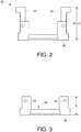
- FIG. 2 shows a typical M.2 connector 20.
- M.2 connector 20 comprises a base 30 and upstanding latches 23, 24.
- the base 30 can be attached to a supporting PCB.
- the latches 23, 24 can provide an overall height for the M.2 connector 20 that may exceed the clearance dimension C of reflow oven 10 in FIG. 1 .
- the M.2 connector 20 of FIG. 2 were placed on conveyor 12 of FIG. 1 in a vertical orientation (as shown in FIG. 2 ), the M.2 connector 20 of FIG. 2 has the potential to come into physical contact with the reflow oven 10 of FIG. 1 .
- M.2 connector 20 of FIG. 2 would either be knocked over on its side, be forcibly compressed within reflow oven 10, or even cause components of the M.2 connector 20 to separate.
- FIG. 3 which shows the base 30 of M.2. connector 20
- the present inventors have observed that the base 30 will have a height "H" that is significantly smaller than a height of the complete M.2. connector 20 shown in FIG. 2 .
- the base 30 alone could enter the reflow oven 10 (in FIG. 1 ) without making any unwanted physical contact.
- the present disclosure leverages this fact to provide various configurations for an M.2 connector and other similar electronic components so as to avoid the unwanted physical contact issues with existing reflow ovens or other treatment devices.
- FIGs. 4A and 4B there is shown an exemplary embodiment for M.2 connector 40 in which a vertical disassembly configuration is provided.
- FIG. 4A shows an assembled arrangement of M.2 connector 40, presenting a height "HT". As discussed above, height "HT" could exceeds the clearance of an existing reflow oven.
- the latches 23 and 24 can be removed from M.2 connector 40 by a vertical motion relative to base 30. This is illustrated in FIG. 4B .
- Each of the resulting smaller components or subassemblies can then fit into an existing reflow oven with a lower risk of unwanted physical contact. After treatment, the components can be reassembled.
- latch 23 can be provided with a boss 25, which fits into aperture 26 of base 30.
- latch 24 can be provided with boss 27, which interfits into aperture 28 in base 30.
- the latches 23, 24 will be retained to the base 30 when the respective bosses 25, 27 are fitted into apertures 26, 28 of base 30 as shown in FIG. 4A .
- the latches 23, 24 can be replaced with latches of different length.
- an M.2 module of the short type could be replaced by the customer with an M.2 module of the long type.
- the latches 23, 24 could be removed from base 30 and replaced by latches of longer length. The customer need not replace the connector, which might be attached to a PCB, but would merely replace the latch.
- the latches can be repositioned via rotation.
- the provision of rotation is permitted due to the presence of pivots 82, 83 in base 30 as shown in FIG. 5A and 5B , which show an exemplary embodiment for an M.2. connector 85 in which pivoting of latching components is provided in order to reduce a height of the M.2 connector.
- the M.2 connector 85 is shown including the optional supporting PCB 50 attached to the base 30.
- the latches 23, 24 are attached to base 30 with pivots 82, 83. Pivots 82, 83 permit each of the latches 23, 24 to rotate relative to base 30. As shown by arrows 80, 81, the latches 23, 24, respectively, are rotated downwardly towards PCB 50 to reduce the overall height of the M.2 connector 85.
- FIG. 6B shows that after treatment, latches 23, 24 can be rotated towards one another, as shown in by arrows 87, 88.
- FIGs. 6A and 6B also show that the rotation of the latches 23, 24 can be used to position and secure an electronic component or module 86 in the M.2 connector 85.
- Module 86 can be, for example, older SATA or PCI-E devices or newer M.2 devices. These can include, but are not limited to memory devices, Wi-Fi/Bluetooth devices, or cellular card devices. However, the various embodiments of the disclosure are not limited to any particular type of device or dimension thereof for module 86.
- securing of a module is not limited to the configuration illustrated in FIGs. 6A and 6B .
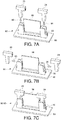
- an M.2. connector can be configured to allow for a vertical or a lateral motion of latches 23, 34, respectively, to secure module 86 in place and still provide a height reduction of the M.2 connector. This is illustrated in FIGs. 7A, 7B and 7C .
- FIG. 7A shows an M.2 connector 90, where the latches 23, 24 may be secured to base 30 by a simple vertical movement, as shown by arrows 91, 92.
- FIG. 7B shows an M.2 connector 95, where the latches 23, 24 may be secured to base 30 by a simple horizontal movement, as shown by arrows 93, 94.
- the removal of latches 23, 24 provides the height reduction needed for heat treatment while still providing a mechanism to secure the module 86 in base 30 after reassembly as shown in FIG. 7C .
- FIG. 8A shows an M.2 connector 100 in which a one-part latch 102 is provided.
- the one-part latch 102 can be joined to connector base 30 by vertical movement.
- the one-part latch 102 can also be used to secure a module 86 to the base 30.
- FIG. 8C shows a module 86 to the base 30.
- the one-part latch 102 can be pivotably attached to an M.2 connector 103.
- FIG. 8B That is, the one-part latch 102 can be configured for rotational movement in the direction of arrow 105.
- a modified base 106 would be used that omits a rearward retaining wall to permit the rotation of one-part latch 102.
- FIG. 9A and 9B the various embodiments are not limited in this regard.
- the one-part latch 102 may be preassembled with module 86 to form a subassembly "module on latch" 110 and heat treated separately from base 30 and supporting PCB 50 (collectively subassembly "module on base” 52).
- the subassemblies 52 and 110 can be reassembled by simple vertical movement in the direction of arrow 111 in FIG. 9B .
Landscapes
- Engineering & Computer Science (AREA)
- Manufacturing & Machinery (AREA)
- Microelectronics & Electronic Packaging (AREA)
- Coupling Device And Connection With Printed Circuit (AREA)
- Electric Connection Of Electric Components To Printed Circuits (AREA)
- Manufacturing Of Electrical Connectors (AREA)
Abstract
Description
- The present invention relates to electronic connectors for computing device, and more specifically to for electronic connectors that facilitating treatment thereof and related methods.
- Many electronic components are now being designed after the existing apparatus to treat the component was designed. In some instances, the treatment apparatus does not have the clearance necessary to permit the component to be treated without unwanted physical contact between the component and the treatment apparatus. That is, the component's dimensions exceed that of the treatment apparatus. One treatment apparatus typically used for computing device components is a reflow oven in which a solder paste is used to temporarily attach one or several electronic components to their contact pads. Afterwards, the entire assembly is subjected to controlled heat, which melts the solder paste to permanently attach the electronic components. However, many reflow ovens only have a limited clearance height, e.g.,30 mm. Thus, use of such reflow ovens can be challenging when the electronic components, alone or aggregately, exceed the oven's clearance height.
- The present disclosure concerns various embodiments for reconfigurable connectors for computing devices adapted for use with limited clearance treatment apparatus, such as reflow ovens. In some embodiments, a vertical M.2 connector (e.g., Memory, PCI-E, Wi-Fi/Bluetooth, WWAN, cellular cards, SATA devices) is provided, where the connector is configured to allow separation of the connector into smaller sized parts or modules (e.g., latch and base). For example, one or more portions of the latch can be configured for vertical or lateral movements relative to the base to disassemble and reassemble the connector. This configuration allows results in smaller parts after disassembly and allows for treatment of these smaller parts in a reflow oven or other treatment apparatus without clearance issues. The connector is also configured so that the treated parts can be easily reassembled after treatment. For example, the connector is configured for disassembly so as to allow the latch to be separately treated from the base, and then reassembled after treatment. In particular embodiments, a module can be inserted into the base before or after treatment and/or reassembly.
- In other embodiments, one or more portions of the latch may be pivotably configured so as to reduce the overall height of the connector to less than the clearance of the reflow oven or other treatment apparatus. For example, one or more parts of the latch are pivotably connected to other parts of the latch. Alternatively, the latch can be pivotably connected to the base.
- In particular embodiments, after treatment of the connector with a pivotable latch, a module may be inserted into the base, and the latch can be rotated to secure the module in the connector. However, the module may also be inserted into the base prior to treatment, with the latch being rotated after treatment to secure the module. In still other embodiments, the latch and module may be joined and heat treated separately from the base.
-
-
FIG. 1 is a perspective view of an existing reflow oven. -
FIG. 2 is a schematic of a typical assembled M.2 connector. -
FIG. 3 is an elevation view of an M.2 connector base. -
FIG 4A is a perspective view of an M.2 connector according to an embodiment. -
FIG. 4B is an exploded view ofFIG. 4A . -
FIG. 5A illustrates an unassembled view of an M.2 connector with a base providing for pivoting latches connected to a PCB according to an embodiment. -
FIG. 5B is an assembled view ofFIG. 5A . -
FIG. 6A illustrates an unassembled view of an M.2 connector with a vertically moving one-part latch according to an embodiment. -
FIG. 6B is an assembled view ofFIG. 6A . -
FIG. 7A is a schematic view illustrating vertical joinder of the latches with the base by vertical motion. -
FIG. 7B is a schematic view illustrating the joining of the latches with the base by horizontal motion. -
FIG. 7C illustrates an assembled view of an M.2 connector with latches according to an embodiment. -
FIG. 8A schematically illustrates a one-part latch joinable with a base by relative vertical motion. -
FIG. 8B schematically illustrates a one-part latch joinable to a base by rotational motion. -
FIG. 8C illustrates the assembled latch and base ofFIG. 8A . -
FIG. 9A is an exploded view illustrating a one-part latch having a device module assembled thereto according to one embodiment. -
FIG. 9B illustrates the joined latch, module and base ofFIG. 9A . - The present invention is described with reference to the attached figures, where like reference numerals are used throughout the figures to designate similar or equivalent elements. The figures are not drawn to scale and are provided merely to illustrate the instant invention. Several aspects of the invention are described below with reference to example applications for illustration. It should be understood that numerous specific details, relationships, and methods are set forth to provide a full understanding of the invention. Those skilled in the art will appreciate that not every element is visible in each figure of the drawings. One having ordinary skill in the relevant art, however, will readily recognize that the invention can be practiced without one or more of the specific details, or with other methods. In other instances, well-known structures or operations are not shown in detail to avoid obscuring the invention. The present invention is not limited by the illustrated ordering of acts or events, as some acts may occur in different orders and/or concurrently with other acts or events. Furthermore, not all illustrated acts or events are required to implement a methodology in accordance with the present invention.
- M.2 (formerly known as the Next Generation Form Factor (NGFF)) is a specification for internally mounted computer expansion cards and associated connectors. It replaces the mSATA standard, which uses the PCI Express mini Card physical card layout and connectors. M.2's more flexible physical specification allows for different module widths and lengths; and makes the M.2 more suitable than mSATA for solid-state storage application in general and particularly for the use in small devices, such as ultrabooks or tablets. Such flexibility in dimensions have not only made the M.2 connector more popular, but has also produced demands by the industry to increase its size. However, existing reflow ovens and other treatment apparatus were sized without taking into account the possible larger dimensions to which the M.2 connectors are currently being manufactured. Thus, it is difficult, or impossible, to feed oversize M.2 connectors through existing reflow ovens or other treatment apparatus without encountering contact interference of the connector and oven clearances. Thus, this disclosure provides several alternatives to treat the oversized M.2 connector and other oversized connectors in existing reflow ovens or other existing treatment apparatus of limited dimensional clearance.
- Although the various embodiments will be described primarily with reference to reflow ovens for M.2 connectors, the present disclosure is not limited in this regard. Rather the present disclosure contemplates that the teachings herein are applicable to configuring any type of electronic components for use with any type of treatment apparatus with a limited size opening or aperture.
- In a reflow oven, a previously applied solder paste liquefies under the heat of the oven and bonds the parts of an M.2 connector. Thus, it is essential that the arrangement of the parts being treated is not disturbed via unwanted physical contact with the oven before the final bond is formed. This challenge is described below with respect to
FIGs. 1 and2 . -
FIG. 1 is a perspective view of an existingreflow oven 10. The reflow oven comprises an aperture oropening 14 and aconveyor 12. Parts can be placed on theconveyor 12 to be conveyed in the reflow oven throughaperture 14. The dimension "C" inFIG. 1 is the limiting clearance for theaperture 14, and thus defines a maximum height of a part on theconveyor 12 to be treated. -
FIG. 2 shows a typical M.2connector 20. M.2connector 20 comprises abase 30 andupstanding latches base 30 can be attached to a supporting PCB. When correctly positioned onbase 30, thelatches connector 20 that may exceed the clearance dimension C ofreflow oven 10 inFIG. 1 . Thus, if the M.2connector 20 ofFIG. 2 were placed onconveyor 12 ofFIG. 1 in a vertical orientation (as shown inFIG. 2 ), the M.2connector 20 ofFIG. 2 has the potential to come into physical contact with thereflow oven 10 ofFIG. 1 . Depending on the degree to which the M.2connector 20 inFIG. 2 exceeds the clearance C ofreflow oven 10 inFIG. 1 , M.2connector 20 ofFIG. 2 would either be knocked over on its side, be forcibly compressed withinreflow oven 10, or even cause components of the M.2connector 20 to separate. - Turning now to
FIG. 3 , which shows thebase 30 of M.2.connector 20, the present inventors have observed that the base 30 will have a height "H" that is significantly smaller than a height of the complete M.2.connector 20 shown inFIG. 2 . Thus, thebase 30 alone could enter the reflow oven 10 (inFIG. 1 ) without making any unwanted physical contact. The present disclosure leverages this fact to provide various configurations for an M.2 connector and other similar electronic components so as to avoid the unwanted physical contact issues with existing reflow ovens or other treatment devices. - Turning first to
FIGs. 4A and 4B , there is shown an exemplary embodiment for M.2connector 40 in which a vertical disassembly configuration is provided.FIG. 4A shows an assembled arrangement of M.2connector 40, presenting a height "HT". As discussed above, height "HT" could exceeds the clearance of an existing reflow oven. In this embodiment, thelatches connector 40 by a vertical motion relative tobase 30. This is illustrated inFIG. 4B . Each of the resulting smaller components or subassemblies can then fit into an existing reflow oven with a lower risk of unwanted physical contact. After treatment, the components can be reassembled. In some embodiments, latch 23 can be provided with aboss 25, which fits intoaperture 26 ofbase 30. Similarly latch 24 can be provided withboss 27, which interfits intoaperture 28 inbase 30. Thelatches respective bosses apertures base 30 as shown inFIG. 4A . In some circumstances, thelatches latches base 30 and replaced by latches of longer length. The customer need not replace the connector, which might be attached to a PCB, but would merely replace the latch. - Alternatively, the latches can be repositioned via rotation. The provision of rotation is permitted due to the presence of
pivots base 30 as shown inFIG. 5A and 5B , which show an exemplary embodiment for an M.2.connector 85 in which pivoting of latching components is provided in order to reduce a height of the M.2 connector. InFIGs. 5A and 5B , the M.2connector 85 is shown including the optional supportingPCB 50 attached to thebase 30. - As shown in
FIG. 6A , thelatches pivots Pivots latches base 30. As shown byarrows latches PCB 50 to reduce the overall height of the M.2connector 85.FIG. 6B shows that after treatment, latches 23, 24 can be rotated towards one another, as shown in byarrows FIGs. 6A and 6B also show that the rotation of thelatches module 86 in the M.2connector 85.Module 86 can be, for example, older SATA or PCI-E devices or newer M.2 devices. These can include, but are not limited to memory devices, Wi-Fi/Bluetooth devices, or cellular card devices. However, the various embodiments of the disclosure are not limited to any particular type of device or dimension thereof formodule 86. - In other embodiments, securing of a module is not limited to the configuration illustrated in
FIGs. 6A and 6B . Rather, the present disclosure contemplates that an M.2. connector can be configured to allow for a vertical or a lateral motion oflatches 23, 34, respectively, to securemodule 86 in place and still provide a height reduction of the M.2 connector. This is illustrated inFIGs. 7A, 7B and 7C . -
FIG. 7A shows an M.2connector 90, where thelatches base 30 by a simple vertical movement, as shown byarrows 91, 92.FIG. 7B shows an M.2connector 95, where thelatches base 30 by a simple horizontal movement, as shown byarrows latches module 86 inbase 30 after reassembly as shown inFIG. 7C . - In other embodiments, securing of a module is not limited to the dual latch configuration described above. Rather, the present disclosure also contemplates that an M.2. connector can be configured to use a one-part latch. This is illustrated in
FIGs. 8A-8C. FIG. 8A shows an M.2connector 100 in which a one-part latch 102 is provided. As shown byarrow 104 inFIG. 8A , the one-part latch 102 can be joined toconnector base 30 by vertical movement. The one-part latch 102 can also be used to secure amodule 86 to thebase 30. This is illustrated inFIG. 8C . Alternatively, the one-part latch 102 can be pivotably attached to an M.2connector 103. This is shown inFIG. 8B . That is, the one-part latch 102 can be configured for rotational movement in the direction ofarrow 105. In this configuration, a modifiedbase 106 would be used that omits a rearward retaining wall to permit the rotation of one-part latch 102. - Although the embodiments in
FIGs. 8A-8C contemplate that a module is already inserted into a base of the M.2 connector, the various embodiments are not limited in this regard. This is shown inFIG. 9A and 9B . As shown inFIG. 9A , the one-part latch 102 may be preassembled withmodule 86 to form a subassembly "module on latch" 110 and heat treated separately frombase 30 and supporting PCB 50 (collectively subassembly "module on base" 52). After heat treatment of thesubassemblies arrow 111 inFIG. 9B . - The terminology used herein is for the purpose of describing particular embodiments only and is not intended to be limiting of the invention. As used herein, the singular forms "a," "an," and "the" are intended to include the plural forms as well, unless the context clearly indicates otherwise. Furthermore, to the extent that the terms "including," "includes," "having," "has," "with," or variants thereof are used in either the detailed description and/or the claims, such terms are intended to be inclusive in a manner similar to the term "comprising."
- Unless otherwise defined, all terms (including technical and scientific terms) used herein have the same meaning as commonly understood by one of ordinary skill in the art to which this invention belongs. Furthermore, terms, such as those defined in commonly used dictionaries, should be interpreted as having a meaning that is consistent with their meaning in the context of the relevant art and will not be interpreted in an idealized or overly formal sense unless expressly so defined herein.
Claims (15)
- A method of heat treating an M.2 connector (20, 40, 85, 90, 95, 100, 103) in a reflow oven (10), wherein the reflow oven (10) has a limited clearance which the assembled M.2 connector exceeds, characterized in that the process comprises:dividing the M.2 connector (20, 40, 85, 90, 95, 100, 103) into subassemblies, each said subassemblies being of a size to fit within the limited clearance;heat treating the subassemblies; and,assembling the heat treated subassemblies into an M.2 connector (20, 40, 85, 90, 95, 100, 103) after the heat treatment.
- The method of claim 1, wherein the step of subdividing the M.2 connector (20 , 40, 85, 90, 95, 100, 103) into subassemblies comprises forming a subassembly of an M.2 connector base (30, 106) and a printed circuit board (50) upon which the M.2 connector base is mounted.
- The method of claim 1, wherein the step of subdividing the M.2 connector (20 , 40, 85, 90, 95, 100, 103) into subassemblies comprises forming a subassembly of at least one latch (23, 24) and an electronic module (86).
- The method of claim 3, wherein said electronic module (86) is one selected from the group consisting of memory, Wi-Fi, Bluetooth, PCI-E, mSATA and cellular cards.
- The method of claim 2, further comprising pivotably mounting a latch (102) to the M.2 connector base (30, 106), and pivoting the latch downwardly to reduce the overall height of the M.2 connector so as to fit within the limited clearance of the reflow oven.
- The method of claim 5, further comprising mounting an electronic module (86) into the M.2 connector base (30, 106) after heat treatment, and pivoting the latch (102) to hold the electronic module (86) to the M.2 connector base (30, 106).
- The method of claim 6, wherein the latch is a one-part latch (102).
- The method of claim 5, further comprising pivotably mounting a second latch (23, 24) to the M.2 connector base (30, 106), and pivoting the second latch (23, 24) downwardly to reduce the overall height of the M.2 connector so as to fit within the limited clearance of the reflow oven (10).
- The method of claim 1, further including adding an electronic module (86) during the assembling step.
- An M.2 connector (20, 40, 85, 90, 95, 100, 103), characterized in that the M.2 connector comprises:an M.2 connector base (30, 106);a pair of latches (23, 24);the pair of latches (23, 24) being pivotably mounted on the connector base (30, 106).
- The M.2 connector of claim 10, further comprising a printed circuit board (50) upon which the M.2 connector base (30, 106) is mounted.
- The M.2 connector of claim 11, wherein the pair of latches (23, 24), when pivoted toward the printed circuit board (50), provides a total height to the M.2 connector which is less than the height of the M.2 connector when the latches (23, 24) are pivoted to a vertical position.
- The M.2 connector of claim 10, further comprising an electronic module (86) mounted to said M.2 connector base (30, 106) and held by said pair of latches (23, 24).
- The M.2 connector of claim 13, wherein the electronic module (86) is up to 110 mm in length.
- An M.2 connector (20, 40, 85, 90, 95, 100, 103), characterized in that the M.2 connector comprises:a first subassembly, the first subassembly comprising an M.2 connector base (30, 106) and a printed circuit board (50) upon which the M.2 connector base (30, 106) is mounted;a second subassembly, the second subassembly comprising a one-part latch (102);each of the first and the second subassemblies being heat treated before the first and second subassemblies are connected to each other.
Applications Claiming Priority (1)
| Application Number | Priority Date | Filing Date | Title |
|---|---|---|---|
| US16/131,924 US10720722B2 (en) | 2018-09-14 | 2018-09-14 | Electronics connector for facilitating treatment |
Publications (2)
| Publication Number | Publication Date |
|---|---|
| EP3624272A1 true EP3624272A1 (en) | 2020-03-18 |
| EP3624272B1 EP3624272B1 (en) | 2021-09-29 |
Family
ID=65812026
Family Applications (1)
| Application Number | Title | Priority Date | Filing Date |
|---|---|---|---|
| EP19161877.6A Active EP3624272B1 (en) | 2018-09-14 | 2019-03-11 | Method of heat treating an m.2 connector |
Country Status (5)
| Country | Link |
|---|---|
| US (1) | US10720722B2 (en) |
| EP (1) | EP3624272B1 (en) |
| JP (1) | JP6835336B2 (en) |
| CN (1) | CN110911879B (en) |
| TW (1) | TWI705631B (en) |
Families Citing this family (17)
| Publication number | Priority date | Publication date | Assignee | Title |
|---|---|---|---|---|
| US11644425B2 (en) | 2019-07-19 | 2023-05-09 | Dell Products L.P. | System and method for optical state determination |
| US11129307B2 (en) | 2019-07-19 | 2021-09-21 | Dell Products L.P. | System and method for managing thermal states of devices |
| US10980159B2 (en) | 2019-07-19 | 2021-04-13 | Dell Products L.P. | System and method for managing multiple connections |
| US10917996B1 (en) | 2019-07-19 | 2021-02-09 | Dell Products L.P. | System and method for device level thermal management and electromagnetic interference management |
| US11378608B2 (en) | 2019-07-19 | 2022-07-05 | Dell Products L.P. | System and method for device state determination |
| US11143682B2 (en) | 2019-07-19 | 2021-10-12 | Dell Products L.P. | System and method for communicating externally from an electromagnetic interference suppressed volume |
| US11132038B2 (en) | 2019-07-19 | 2021-09-28 | Dell Products L.P. | System and method for thermal management of shadowed devices |
| US11122718B2 (en) | 2019-07-19 | 2021-09-14 | Dell Products L.P. | System and method for device level electromagnetic interference management |
| US11399450B2 (en) | 2019-07-19 | 2022-07-26 | Dell Products L.P. | System and method for managing electromagnetic interference |
| US12004336B2 (en) | 2019-07-19 | 2024-06-04 | Dell Products L.P. | System and method for thermal management and electromagnetic interference management |
| US11234347B2 (en) * | 2019-07-19 | 2022-01-25 | Dell Products L.P. | System and method for physical management of devices |
| US11147194B2 (en) | 2019-08-21 | 2021-10-12 | Dell Products L.P. | System and method for managing electromagnetic interference |
| US11234350B2 (en) | 2019-08-21 | 2022-01-25 | Dell Products L.P. | System and method for isolated device access |
| US11228126B2 (en) * | 2020-01-09 | 2022-01-18 | Intel Corporation | Dual in-line memory modules (DIMM) connector towers with removable and/or lay-flat latches |
| CN113410728B (en) * | 2021-08-20 | 2021-11-16 | 深圳泰思特半导体有限公司 | Mounting system of precision memory |
| US12095217B2 (en) * | 2022-04-06 | 2024-09-17 | Quanta Computer Inc. | Cable release device and method for releasing a cable |
| WO2024080999A1 (en) * | 2022-10-14 | 2024-04-18 | Hewlett-Packard Development Company, L.P. | Card connectors |
Citations (3)
| Publication number | Priority date | Publication date | Assignee | Title |
|---|---|---|---|---|
| EP0926779A1 (en) * | 1997-12-23 | 1999-06-30 | Berg Electronics Manufacturing B.V. | High density edge card connector and method of making the same |
| US7488192B1 (en) * | 2008-01-10 | 2009-02-10 | International Business Machines Corporation | Apparatus and method that minimizing dimensional instability and solder stress in surface mounted interconnections |
| CN207853057U (en) * | 2018-03-09 | 2018-09-11 | 安费诺商用电子产品(成都)有限公司 | Self-locking M.2 connector |
Family Cites Families (37)
| Publication number | Priority date | Publication date | Assignee | Title |
|---|---|---|---|---|
| JPS5633107Y2 (en) * | 1975-10-13 | 1981-08-06 | ||
| US4858309A (en) * | 1988-06-28 | 1989-08-22 | Amp Incorporated | Extraction tool |
| US5318452A (en) * | 1992-08-10 | 1994-06-07 | The Whitaker Corporation | Electrical connector |
| US6276950B1 (en) * | 1994-12-21 | 2001-08-21 | Berg Technology, Inc. | Socket for printed circuit board |
| JPH11505957A (en) * | 1995-05-26 | 1999-05-25 | ランバス・インコーポレーテッド | Chip socket assembly and chip file assembly for semiconductor chips |
| US5762513A (en) * | 1996-06-18 | 1998-06-09 | The Whitaker Corporation | Electrical connector assembly |
| US5676561A (en) * | 1996-11-05 | 1997-10-14 | Nextronics Engineering Co., Ltd. | Edge card connector having guide units with sufficient resiliency |
| JPH11233194A (en) * | 1997-07-23 | 1999-08-27 | Whitaker Corp:The | Circuit card holder and connector assembly using the same |
| US5943218A (en) * | 1998-06-01 | 1999-08-24 | Liu; Yen-Wen | Card type CPU-fixing structure |
| US6059585A (en) * | 1998-10-29 | 2000-05-09 | Starlink Electronics Corp. | Electric connector |
| TW417868U (en) * | 1998-11-06 | 2001-01-01 | Hon Hai Prec Ind Co Ltd | Auxiliary installation apparatus for electric card connector |
| TW392945U (en) * | 1998-12-31 | 2000-06-01 | Hon Hai Prec Ind Co Ltd | Holder |
| CN2379937Y (en) * | 1999-07-08 | 2000-05-24 | 富士康(昆山)电脑接插件有限公司 | Electric connecting means compound |
| TW453537U (en) * | 2000-09-29 | 2001-09-01 | Hon Hai Prec Ind Co Ltd | Connector device |
| US6887095B2 (en) * | 2002-12-30 | 2005-05-03 | Intel Corporation | Electromagnetic coupler registration and mating |
| CN2838079Y (en) * | 2005-06-27 | 2006-11-15 | 莫列斯公司 | Card edge connector locking device |
| CN200959422Y (en) * | 2006-08-25 | 2007-10-10 | 富士康(昆山)电脑接插件有限公司 | electrical connector |
| WO2008091877A1 (en) * | 2007-01-23 | 2008-07-31 | 3M Innovative Properties Company | Electrical connector |
| US20120149223A1 (en) * | 2010-12-13 | 2012-06-14 | 3M Innovative Properties Company | Electrical connector having lever |
| US8369080B2 (en) * | 2011-02-25 | 2013-02-05 | Jui-Shu Huang | Removable hard disk drive bay |
| CN102761028A (en) * | 2011-04-28 | 2012-10-31 | 鸿富锦精密工业(深圳)有限公司 | Board card fixing device |
| CN102544884B (en) * | 2011-12-23 | 2015-04-01 | 富士康(昆山)电脑接插件有限公司 | Electric connector, electric connector casing and surface treatment method of electric connector casing |
| CN104205507B (en) * | 2012-02-07 | 2017-06-13 | 3M创新有限公司 | Board mounted electrical connector |
| US8636528B2 (en) * | 2012-04-27 | 2014-01-28 | International Business Machines Corporation | Memory module connector with latch assist |
| CN103972728B (en) * | 2013-01-29 | 2016-08-31 | 富士康(昆山)电脑接插件有限公司 | Bayonet connector |
| TWI532260B (en) * | 2013-10-14 | 2016-05-01 | 技嘉科技股份有限公司 | Card edge connector |
| WO2015084316A1 (en) * | 2013-12-02 | 2015-06-11 | Hewlett Packard Development Company, L.P. | Connector component |
| CN204045780U (en) * | 2014-07-18 | 2014-12-24 | 富士康(昆山)电脑接插件有限公司 | Electric connector and assembly thereof |
| TW201711305A (en) | 2015-09-10 | 2017-03-16 | 宜鼎國際股份有限公司 | M.2 interface connector and M.2 interface seat insertedly provided thereof |
| TWI573337B (en) * | 2015-12-17 | 2017-03-01 | 宜鼎國際股份有限公司 | M.2 interface memory device and m.2 interface connection seat insertedly provided thereof |
| US10064299B2 (en) * | 2015-12-30 | 2018-08-28 | Quanta Computer Inc. | Component quick release |
| US9640910B1 (en) * | 2016-05-02 | 2017-05-02 | Dell Products L.P. | Apparatus for securing connection between cable assembly and storage device connector |
| US10193248B2 (en) * | 2016-08-31 | 2019-01-29 | Crystal Group, Inc. | System and method for retaining memory modules |
| TWI619421B (en) * | 2016-10-06 | 2018-03-21 | 技嘉科技股份有限公司 | Interface card fixing device and main board module |
| TWI683610B (en) * | 2016-10-07 | 2020-01-21 | 美商利魁得股份有限公司 | Modular carrier form factors for computing platforms |
| US10054992B1 (en) * | 2017-08-22 | 2018-08-21 | Facebook, Inc. | Storage card adapter with latch |
| CN107658584B (en) * | 2017-08-28 | 2019-06-18 | 番禺得意精密电子工业有限公司 | Connector |
-
2018
- 2018-09-14 US US16/131,924 patent/US10720722B2/en active Active
-
2019
- 2019-01-28 TW TW108103155A patent/TWI705631B/en active
- 2019-02-25 CN CN201910136936.XA patent/CN110911879B/en active Active
- 2019-03-11 EP EP19161877.6A patent/EP3624272B1/en active Active
- 2019-04-23 JP JP2019081437A patent/JP6835336B2/en active Active
Patent Citations (3)
| Publication number | Priority date | Publication date | Assignee | Title |
|---|---|---|---|---|
| EP0926779A1 (en) * | 1997-12-23 | 1999-06-30 | Berg Electronics Manufacturing B.V. | High density edge card connector and method of making the same |
| US7488192B1 (en) * | 2008-01-10 | 2009-02-10 | International Business Machines Corporation | Apparatus and method that minimizing dimensional instability and solder stress in surface mounted interconnections |
| CN207853057U (en) * | 2018-03-09 | 2018-09-11 | 安费诺商用电子产品(成都)有限公司 | Self-locking M.2 connector |
Non-Patent Citations (1)
| Title |
|---|
| ATTEND TECHNOLOGIES: "M.2 Connector (NGFF) Introduction", 3 February 2014 (2014-02-03), XP055624301, Retrieved from the Internet <URL:https://web.archive.org/web/20140203000954if_/http://www.orvem.eu/attachments/article/130/M%202%20introduction.pdf> [retrieved on 20190919] * |
Also Published As
| Publication number | Publication date |
|---|---|
| US10720722B2 (en) | 2020-07-21 |
| US20200091640A1 (en) | 2020-03-19 |
| TW202011652A (en) | 2020-03-16 |
| JP6835336B2 (en) | 2021-02-24 |
| CN110911879A (en) | 2020-03-24 |
| JP2020047578A (en) | 2020-03-26 |
| EP3624272B1 (en) | 2021-09-29 |
| CN110911879B (en) | 2021-08-24 |
| TWI705631B (en) | 2020-09-21 |
Similar Documents
| Publication | Publication Date | Title |
|---|---|---|
| US10720722B2 (en) | Electronics connector for facilitating treatment | |
| JP2006100302A (en) | High frequency module and manufacturing method thereof | |
| US11348877B2 (en) | RF shielding can with integral spring fingers | |
| EP3314994B1 (en) | Modular radio frequency shielding | |
| US10664431B2 (en) | Advanced PCI express board assembly | |
| DE112024001813T5 (en) | WIRELESS NANO RECEIVER DONGLE | |
| EP1248322A3 (en) | Mounting structure of connector for use with curcuit board | |
| US3673669A (en) | Method of making side entry card guides | |
| US20160028173A1 (en) | Printed circuit board connector for non-planar configurations | |
| US20150097737A1 (en) | Modular antenna assemblies for wireless systems | |
| WO1999014828A1 (en) | Recyclable locator device for board mounted connectors | |
| US20170019997A1 (en) | Integrated PCB Interconnect System | |
| EP3082330A1 (en) | Mainboard structure and terminal | |
| US6817878B2 (en) | Zero mounting force solder-free connector/component and method | |
| CN103326148A (en) | Plug-in type component, circuit board and preparation method for circuit board | |
| CN101237766B (en) | PCB carrier | |
| CN103712181B (en) | A kind of LED erecting device and installation method and prepared display device thereof | |
| WO2014026477A1 (en) | Secure digital card device | |
| US9978706B2 (en) | Ball grid array rework | |
| CN220006545U (en) | Circuit board welding tool | |
| US20050061543A1 (en) | Component lead system | |
| US20110296677A1 (en) | Rework soldering jig | |
| CN115914807B (en) | Anti-shake mechanism, camera module and electronic equipment | |
| US9583852B1 (en) | PCB holder having a leg with a passageway with a conductive pin therein to electrically connect two PCBs | |
| CN108832282A (en) | Antenna assembly for comprehensive screen mobile phone high-gain |
Legal Events
| Date | Code | Title | Description |
|---|---|---|---|
| PUAI | Public reference made under article 153(3) epc to a published international application that has entered the european phase |
Free format text: ORIGINAL CODE: 0009012 |
|
| STAA | Information on the status of an ep patent application or granted ep patent |
Free format text: STATUS: REQUEST FOR EXAMINATION WAS MADE |
|
| 17P | Request for examination filed |
Effective date: 20200114 |
|
| AK | Designated contracting states |
Kind code of ref document: A1 Designated state(s): AL AT BE BG CH CY CZ DE DK EE ES FI FR GB GR HR HU IE IS IT LI LT LU LV MC MK MT NL NO PL PT RO RS SE SI SK SM TR |
|
| AX | Request for extension of the european patent |
Extension state: BA ME |
|
| GRAP | Despatch of communication of intention to grant a patent |
Free format text: ORIGINAL CODE: EPIDOSNIGR1 |
|
| STAA | Information on the status of an ep patent application or granted ep patent |
Free format text: STATUS: GRANT OF PATENT IS INTENDED |
|
| RIC1 | Information provided on ipc code assigned before grant |
Ipc: H01R 12/71 20110101AFI20210323BHEP Ipc: H01R 43/02 20060101ALI20210323BHEP Ipc: H01R 13/627 20060101ALI20210323BHEP Ipc: H05K 3/34 20060101ALI20210323BHEP Ipc: H01R 13/514 20060101ALN20210323BHEP Ipc: H01R 13/629 20060101ALN20210323BHEP |
|
| RIC1 | Information provided on ipc code assigned before grant |
Ipc: H01R 12/71 20110101AFI20210331BHEP Ipc: H01R 43/02 20060101ALI20210331BHEP Ipc: H01R 13/627 20060101ALI20210331BHEP Ipc: H05K 3/34 20060101ALI20210331BHEP Ipc: H01R 13/514 20060101ALN20210331BHEP Ipc: H01R 13/629 20060101ALN20210331BHEP |
|
| INTG | Intention to grant announced |
Effective date: 20210414 |
|
| GRAS | Grant fee paid |
Free format text: ORIGINAL CODE: EPIDOSNIGR3 |
|
| GRAA | (expected) grant |
Free format text: ORIGINAL CODE: 0009210 |
|
| STAA | Information on the status of an ep patent application or granted ep patent |
Free format text: STATUS: THE PATENT HAS BEEN GRANTED |
|
| AK | Designated contracting states |
Kind code of ref document: B1 Designated state(s): AL AT BE BG CH CY CZ DE DK EE ES FI FR GB GR HR HU IE IS IT LI LT LU LV MC MK MT NL NO PL PT RO RS SE SI SK SM TR |
|
| REG | Reference to a national code |
Ref country code: GB Ref legal event code: FG4D |
|
| REG | Reference to a national code |
Ref country code: DE Ref legal event code: R096 Ref document number: 602019007909 Country of ref document: DE |
|
| REG | Reference to a national code |
Ref country code: CH Ref legal event code: EP Ref country code: AT Ref legal event code: REF Ref document number: 1435023 Country of ref document: AT Kind code of ref document: T Effective date: 20211015 |
|
| REG | Reference to a national code |
Ref country code: IE Ref legal event code: FG4D |
|
| REG | Reference to a national code |
Ref country code: LT Ref legal event code: MG9D |
|
| PG25 | Lapsed in a contracting state [announced via postgrant information from national office to epo] |
Ref country code: NO Free format text: LAPSE BECAUSE OF FAILURE TO SUBMIT A TRANSLATION OF THE DESCRIPTION OR TO PAY THE FEE WITHIN THE PRESCRIBED TIME-LIMIT Effective date: 20211229 Ref country code: HR Free format text: LAPSE BECAUSE OF FAILURE TO SUBMIT A TRANSLATION OF THE DESCRIPTION OR TO PAY THE FEE WITHIN THE PRESCRIBED TIME-LIMIT Effective date: 20210929 Ref country code: BG Free format text: LAPSE BECAUSE OF FAILURE TO SUBMIT A TRANSLATION OF THE DESCRIPTION OR TO PAY THE FEE WITHIN THE PRESCRIBED TIME-LIMIT Effective date: 20211229 Ref country code: LT Free format text: LAPSE BECAUSE OF FAILURE TO SUBMIT A TRANSLATION OF THE DESCRIPTION OR TO PAY THE FEE WITHIN THE PRESCRIBED TIME-LIMIT Effective date: 20210929 Ref country code: FI Free format text: LAPSE BECAUSE OF FAILURE TO SUBMIT A TRANSLATION OF THE DESCRIPTION OR TO PAY THE FEE WITHIN THE PRESCRIBED TIME-LIMIT Effective date: 20210929 Ref country code: SE Free format text: LAPSE BECAUSE OF FAILURE TO SUBMIT A TRANSLATION OF THE DESCRIPTION OR TO PAY THE FEE WITHIN THE PRESCRIBED TIME-LIMIT Effective date: 20210929 Ref country code: RS Free format text: LAPSE BECAUSE OF FAILURE TO SUBMIT A TRANSLATION OF THE DESCRIPTION OR TO PAY THE FEE WITHIN THE PRESCRIBED TIME-LIMIT Effective date: 20210929 |
|
| REG | Reference to a national code |
Ref country code: NL Ref legal event code: MP Effective date: 20210929 |
|
| REG | Reference to a national code |
Ref country code: AT Ref legal event code: MK05 Ref document number: 1435023 Country of ref document: AT Kind code of ref document: T Effective date: 20210929 |
|
| PG25 | Lapsed in a contracting state [announced via postgrant information from national office to epo] |
Ref country code: LV Free format text: LAPSE BECAUSE OF FAILURE TO SUBMIT A TRANSLATION OF THE DESCRIPTION OR TO PAY THE FEE WITHIN THE PRESCRIBED TIME-LIMIT Effective date: 20210929 Ref country code: GR Free format text: LAPSE BECAUSE OF FAILURE TO SUBMIT A TRANSLATION OF THE DESCRIPTION OR TO PAY THE FEE WITHIN THE PRESCRIBED TIME-LIMIT Effective date: 20211230 |
|
| PG25 | Lapsed in a contracting state [announced via postgrant information from national office to epo] |
Ref country code: AT Free format text: LAPSE BECAUSE OF FAILURE TO SUBMIT A TRANSLATION OF THE DESCRIPTION OR TO PAY THE FEE WITHIN THE PRESCRIBED TIME-LIMIT Effective date: 20210929 |
|
| PG25 | Lapsed in a contracting state [announced via postgrant information from national office to epo] |
Ref country code: IS Free format text: LAPSE BECAUSE OF FAILURE TO SUBMIT A TRANSLATION OF THE DESCRIPTION OR TO PAY THE FEE WITHIN THE PRESCRIBED TIME-LIMIT Effective date: 20220129 Ref country code: SK Free format text: LAPSE BECAUSE OF FAILURE TO SUBMIT A TRANSLATION OF THE DESCRIPTION OR TO PAY THE FEE WITHIN THE PRESCRIBED TIME-LIMIT Effective date: 20210929 Ref country code: RO Free format text: LAPSE BECAUSE OF FAILURE TO SUBMIT A TRANSLATION OF THE DESCRIPTION OR TO PAY THE FEE WITHIN THE PRESCRIBED TIME-LIMIT Effective date: 20210929 Ref country code: PT Free format text: LAPSE BECAUSE OF FAILURE TO SUBMIT A TRANSLATION OF THE DESCRIPTION OR TO PAY THE FEE WITHIN THE PRESCRIBED TIME-LIMIT Effective date: 20220131 Ref country code: PL Free format text: LAPSE BECAUSE OF FAILURE TO SUBMIT A TRANSLATION OF THE DESCRIPTION OR TO PAY THE FEE WITHIN THE PRESCRIBED TIME-LIMIT Effective date: 20210929 Ref country code: NL Free format text: LAPSE BECAUSE OF FAILURE TO SUBMIT A TRANSLATION OF THE DESCRIPTION OR TO PAY THE FEE WITHIN THE PRESCRIBED TIME-LIMIT Effective date: 20210929 Ref country code: ES Free format text: LAPSE BECAUSE OF FAILURE TO SUBMIT A TRANSLATION OF THE DESCRIPTION OR TO PAY THE FEE WITHIN THE PRESCRIBED TIME-LIMIT Effective date: 20210929 Ref country code: EE Free format text: LAPSE BECAUSE OF FAILURE TO SUBMIT A TRANSLATION OF THE DESCRIPTION OR TO PAY THE FEE WITHIN THE PRESCRIBED TIME-LIMIT Effective date: 20210929 Ref country code: CZ Free format text: LAPSE BECAUSE OF FAILURE TO SUBMIT A TRANSLATION OF THE DESCRIPTION OR TO PAY THE FEE WITHIN THE PRESCRIBED TIME-LIMIT Effective date: 20210929 Ref country code: AL Free format text: LAPSE BECAUSE OF FAILURE TO SUBMIT A TRANSLATION OF THE DESCRIPTION OR TO PAY THE FEE WITHIN THE PRESCRIBED TIME-LIMIT Effective date: 20210929 |
|
| REG | Reference to a national code |
Ref country code: DE Ref legal event code: R097 Ref document number: 602019007909 Country of ref document: DE |
|
| PG25 | Lapsed in a contracting state [announced via postgrant information from national office to epo] |
Ref country code: DK Free format text: LAPSE BECAUSE OF FAILURE TO SUBMIT A TRANSLATION OF THE DESCRIPTION OR TO PAY THE FEE WITHIN THE PRESCRIBED TIME-LIMIT Effective date: 20210929 |
|
| PLBE | No opposition filed within time limit |
Free format text: ORIGINAL CODE: 0009261 |
|
| STAA | Information on the status of an ep patent application or granted ep patent |
Free format text: STATUS: NO OPPOSITION FILED WITHIN TIME LIMIT |
|
| 26N | No opposition filed |
Effective date: 20220630 |
|
| PG25 | Lapsed in a contracting state [announced via postgrant information from national office to epo] |
Ref country code: MC Free format text: LAPSE BECAUSE OF FAILURE TO SUBMIT A TRANSLATION OF THE DESCRIPTION OR TO PAY THE FEE WITHIN THE PRESCRIBED TIME-LIMIT Effective date: 20210929 |
|
| REG | Reference to a national code |
Ref country code: CH Ref legal event code: PL |
|
| PG25 | Lapsed in a contracting state [announced via postgrant information from national office to epo] |
Ref country code: SI Free format text: LAPSE BECAUSE OF FAILURE TO SUBMIT A TRANSLATION OF THE DESCRIPTION OR TO PAY THE FEE WITHIN THE PRESCRIBED TIME-LIMIT Effective date: 20210929 |
|
| REG | Reference to a national code |
Ref country code: BE Ref legal event code: MM Effective date: 20220331 |
|
| PG25 | Lapsed in a contracting state [announced via postgrant information from national office to epo] |
Ref country code: LU Free format text: LAPSE BECAUSE OF NON-PAYMENT OF DUE FEES Effective date: 20220311 Ref country code: LI Free format text: LAPSE BECAUSE OF NON-PAYMENT OF DUE FEES Effective date: 20220331 Ref country code: IT Free format text: LAPSE BECAUSE OF FAILURE TO SUBMIT A TRANSLATION OF THE DESCRIPTION OR TO PAY THE FEE WITHIN THE PRESCRIBED TIME-LIMIT Effective date: 20210929 Ref country code: IE Free format text: LAPSE BECAUSE OF NON-PAYMENT OF DUE FEES Effective date: 20220311 Ref country code: CH Free format text: LAPSE BECAUSE OF NON-PAYMENT OF DUE FEES Effective date: 20220331 |
|
| PG25 | Lapsed in a contracting state [announced via postgrant information from national office to epo] |
Ref country code: BE Free format text: LAPSE BECAUSE OF NON-PAYMENT OF DUE FEES Effective date: 20220331 |
|
| P01 | Opt-out of the competence of the unified patent court (upc) registered |
Effective date: 20230526 |
|
| PG25 | Lapsed in a contracting state [announced via postgrant information from national office to epo] |
Ref country code: SM Free format text: LAPSE BECAUSE OF FAILURE TO SUBMIT A TRANSLATION OF THE DESCRIPTION OR TO PAY THE FEE WITHIN THE PRESCRIBED TIME-LIMIT Effective date: 20210929 Ref country code: MK Free format text: LAPSE BECAUSE OF FAILURE TO SUBMIT A TRANSLATION OF THE DESCRIPTION OR TO PAY THE FEE WITHIN THE PRESCRIBED TIME-LIMIT Effective date: 20210929 Ref country code: CY Free format text: LAPSE BECAUSE OF FAILURE TO SUBMIT A TRANSLATION OF THE DESCRIPTION OR TO PAY THE FEE WITHIN THE PRESCRIBED TIME-LIMIT Effective date: 20210929 |
|
| PG25 | Lapsed in a contracting state [announced via postgrant information from national office to epo] |
Ref country code: HU Free format text: LAPSE BECAUSE OF FAILURE TO SUBMIT A TRANSLATION OF THE DESCRIPTION OR TO PAY THE FEE WITHIN THE PRESCRIBED TIME-LIMIT; INVALID AB INITIO Effective date: 20190311 |
|
| PG25 | Lapsed in a contracting state [announced via postgrant information from national office to epo] |
Ref country code: MT Free format text: LAPSE BECAUSE OF FAILURE TO SUBMIT A TRANSLATION OF THE DESCRIPTION OR TO PAY THE FEE WITHIN THE PRESCRIBED TIME-LIMIT Effective date: 20210929 |
|
| PG25 | Lapsed in a contracting state [announced via postgrant information from national office to epo] |
Ref country code: TR Free format text: LAPSE BECAUSE OF FAILURE TO SUBMIT A TRANSLATION OF THE DESCRIPTION OR TO PAY THE FEE WITHIN THE PRESCRIBED TIME-LIMIT Effective date: 20210929 |
|
| PGFP | Annual fee paid to national office [announced via postgrant information from national office to epo] |
Ref country code: GB Payment date: 20260128 Year of fee payment: 8 |
|
| PGFP | Annual fee paid to national office [announced via postgrant information from national office to epo] |
Ref country code: DE Payment date: 20260121 Year of fee payment: 8 |
|
| PGFP | Annual fee paid to national office [announced via postgrant information from national office to epo] |
Ref country code: FR Payment date: 20260121 Year of fee payment: 8 |