EP3624267A1 - Antenna device - Google Patents
Antenna device Download PDFInfo
- Publication number
- EP3624267A1 EP3624267A1 EP19195749.7A EP19195749A EP3624267A1 EP 3624267 A1 EP3624267 A1 EP 3624267A1 EP 19195749 A EP19195749 A EP 19195749A EP 3624267 A1 EP3624267 A1 EP 3624267A1
- Authority
- EP
- European Patent Office
- Prior art keywords
- region
- conductive layer
- thickness
- substrate
- insulating layer
- Prior art date
- Legal status (The legal status is an assumption and is not a legal conclusion. Google has not performed a legal analysis and makes no representation as to the accuracy of the status listed.)
- Granted
Links
Images


Classifications
-
- H—ELECTRICITY
- H01—ELECTRIC ELEMENTS
- H01Q—ANTENNAS, i.e. RADIO AERIALS
- H01Q3/00—Arrangements for changing or varying the orientation or the shape of the directional pattern of the waves radiated from an antenna or antenna system
- H01Q3/44—Arrangements for changing or varying the orientation or the shape of the directional pattern of the waves radiated from an antenna or antenna system varying the electric or magnetic characteristics of reflecting, refracting, or diffracting devices associated with the radiating element
-
- H—ELECTRICITY
- H01—ELECTRIC ELEMENTS
- H01Q—ANTENNAS, i.e. RADIO AERIALS
- H01Q1/00—Details of, or arrangements associated with, antennas
- H01Q1/36—Structural form of radiating elements, e.g. cone, spiral, umbrella; Particular materials used therewith
-
- H—ELECTRICITY
- H01—ELECTRIC ELEMENTS
- H01Q—ANTENNAS, i.e. RADIO AERIALS
- H01Q9/00—Electrically-short antennas having dimensions not more than twice the operating wavelength and consisting of conductive active radiating elements
- H01Q9/04—Resonant antennas
- H01Q9/0407—Substantially flat resonant element parallel to ground plane, e.g. patch antenna
-
- G—PHYSICS
- G09—EDUCATION; CRYPTOGRAPHY; DISPLAY; ADVERTISING; SEALS
- G09G—ARRANGEMENTS OR CIRCUITS FOR CONTROL OF INDICATING DEVICES USING STATIC MEANS TO PRESENT VARIABLE INFORMATION
- G09G2300/00—Aspects of the constitution of display devices
- G09G2300/08—Active matrix structure, i.e. with use of active elements, inclusive of non-linear two terminal elements, in the pixels together with light emitting or modulating elements
- G09G2300/0876—Supplementary capacities in pixels having special driving circuits and electrodes instead of being connected to common electrode or ground; Use of additional capacitively coupled compensation electrodes
Definitions
- the present disclosure relates to an electronic device, and in particular it relates to an antenna having an insulating structure with varied thickness.
- Electronic products that come with a display panel such as smartphones, tablets, notebooks, monitors, and TVs, have become indispensable necessities in modern society. With the flourishing development of such portable electronic products, consumers have high expectations regarding the quality, functionality, or price of such products.
- Such electronic products can generally be used as electronic modulation devices as well, for example, as antenna devices that can modulate electromagnetic waves.
- an antenna device includes a first substrate, a first conductive layer, a first insulating structure, a second substrate, a second conductive layer and a liquid-crystal layer.
- the first conductive layer is disposed on the first substrate.
- the first insulating structure is disposed on the first conductive layer, and the first insulating structure includes a first region and a second region.
- the second substrate is disposed opposite to the first substrate.
- the second conductive layer is disposed on the second substrate.
- the liquid-crystal layer is disposed between the first conductive layer and the second conductive layer.
- the thickness of the first region is less than the thickness of the second region, and at least a portion of the first region is disposed in an overlapping region of the first conductive layer and the second conductive layer.
- first, second, third etc. may be used herein to describe various elements, components, regions, layers, portions and/or sections, these elements, components, regions, layers, portions and/or sections should not be limited by these terms. These terms are only used to distinguish one element, component, region, layer, portion or section from another region, layer or section. Thus, a first element, component, region, layer, portion or section discussed below could be termed a second element, component, region, layer, portion or section without departing from the teachings of the present disclosure.
- the terms “about” and “substantially” typically mean +/- 20% of the stated value, more typically +/- 10% of the stated value, more typically +/- 5% of the stated value, more typically +/- 3% of the stated value, more typically +/- 2% of the stated value, more typically +/- 1% of the stated value and even more typically +/- 0.5% of the stated value.
- the stated value of the present disclosure is an approximate value. When there is no specific description, the stated value includes the meaning of "about” or “substantially”.
- the phrase “in a range between a first value and a second value” or “in a range from a first value to a second value” indicates that the range includes the first value, the second value, and other values between them.
- attachments, coupling and the like refer to a relationship wherein structures are secured or attached to one another either directly or indirectly through intervening structures, as well as both movable or rigid attachments or relationships, unless expressly described otherwise.
- an electronic device e.g., an antenna device having an insulating structure with varied thickness
- the insulating structure may have a smaller thickness in a portion corresponding to the capacitance adjustable region, thereby maintaining stability of capacitance modulation or increasing operational reliability of the device.
- the insulating structure may have a greater thickness in a portion other than the capacitance adjustable region, which may reduce the risk of corrosion of the conductive layer or diffusion of metal ions.
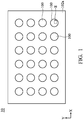
- FIG. 1 illustrates a top-view diagram of an electronic device 10 in accordance with some embodiments of the present disclosure. It should be understood that only some of the components of the electronic device 10 are shown in FIG. 1 and other components are omitted for clarity of illustration. The structure of other components will be described in detail in the following figures. In accordance with some embodiments of the present disclosure, additional features may be added to the electronic device 10 described below.
- the electronic device 10 may include a first substrate 102a and a plurality of electronic units 100 disposed on the first substrate 102a.
- the electronic device 10 may include an antenna device, a display device (e.g., a liquid-crystal display (LCD)), a light-emitting device, a detecting device, or another device for modulating electromagnetic waves, but it is not limited thereto.
- the electronic device 10 mat be an antenna device, and the electronic unit 100 may be an antenna unit for modulating electromagnetic waves (e.g., microwaves). It should be understood that the arrangement of the electronic units 100 is not limited to the aspect shown in FIG. 1 . In accordance with some other embodiments, the electronic units 100 may be arranged in another suitable manner.
- the material of the first substrate 102a may include, but is not limited to, glass, quartz, sapphire, ceramic, polyimide (PI), liquid-crystal polymer (LCP) materials, polycarbonate (PC), photo sensitive polyimide (PSPI), polyethylene terephthalate (PET), other suitable substrate materials, or a combination thereof.
- the first substrate 102a may include a flexible substrate, a rigid substrate, or a combination thereof.
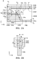
- FIG. 2A illustrates a cross-sectional structural diagram of a portion of the electronic device 10 in accordance with some embodiments of the present disclosure.
- FIG. 2A illustrates an enlarged cross-sectional diagram of a region E of the electronic unit 100 shown in FIG. 1 in accordance with some embodiments of the present disclosure.
- the electronic device 10 may include a first substrate 102a, a second substrate 102b, a first conductive layer 104a, and a second conductive layer 104b.
- the second substrate 102b may be disposed opposite to the first substrate 102a.
- the material of the second substrate 102b may include, but is not limited to, glass, quartz, sapphire, ceramic, polyimide (PI), liquid-crystal polymer (LCP) materials, polycarbonate (PC), photo-sensitive polyimide (PSPI), polyethylene terephthalate (PET), other suitable substrate materials, or a combination thereof.
- the second substrate 102b may include a flexible substrate, a rigid substrate, or a combination thereof.
- the material of the second substrate 102b may be the same as or different from the material of the first substrate 102a.
- the first conductive layer 104a may be disposed on the first substrate 102a. Specifically, the first conductive layer 104a may be disposed on a first surface S 1 of the first substrate 102a, and the first surface S 1 and a second surface S 2 of the first substrate 102a are located on opposite sides.
- the second conductive layer 104b may be disposed on the second substrate 102b and located between the first substrate 102a and the second substrate 102b. Specifically, the second conductive layer 104b may be disposed on the first surface S 1 of the second substrate 102b, and the first surface S 1 of the second substrate 102b is adjacent to the first substrate 102a.
- the first conductive layer 104a may have an opening 104p, and the opening 104p may overlap the second conductive layer 104b.
- the opening 104p may be defined as a region that is exposed by the first conductive layer 104a. That is, the opening 104p may substantially correspond to the region of the first surface S 1 of the first substrate 102a that is not covered by the first conductive layer 104a.
- the second conductive layer 104b may overlap the first conductive layer 104a.
- overlap may include partial overlap or entire overlap in the normal direction of the first substrate 102a or the second substrate 102b (e.g., the Z direction shown in the figure).
- the first conductive layer 104a may be patterned to have an opening 104p.
- the second conductive layer 104b may also be patterned to have multiple regions (only a portion of the second conductive layer 104b is illustrated in the figure). In some embodiments, multiple regions of the second conductive layer 104b may be connected to different circuits.
- the second conductive layer 104b may be electrically connected to a functional circuit (not illustrated).
- the functional circuit may include active components (e.g., thin film transistors and/or chips) or passive components.
- the functional circuit may be located on the first surface S 1 of the second substrate 102b as the second conductive layer 104b.
- the functional circuit may be located on the second surface S 2 of the second substrate 102b, and the functional circuit may be electrically connected to the second conductive layer 104b, for example, through a via hole (not illustrated) that penetrates the second substrate 102b, a flexible circuit board, or another suitable method for electrical connection, but it is not limited thereto.
- the first conductive layer 104a and the second conductive layer 104b may include a conductive metal material.
- the materials of the first conductive layer 104a and the second conductive layer 104b may include, but are not limited to, copper, silver, tin, aluminum, molybdenum, tungsten, gold, chromium, nickel, platinum, copper alloy, silver alloy, tin alloy, aluminum alloy, molybdenum alloy, tungsten alloy, gold alloy, chromium alloy, nickel alloy, platinum alloy, other suitable conductive materials or a combination thereof.
- the first conductive layer 104a may have a thickness T'
- the second conductive layer 104b may have a thickness T".
- the thickness T' of the first conductive layer 104a may be in a range from 0.5 micrometers ( ⁇ m) to 4 micrometers ( ⁇ m) (i.e. 0.5 ⁇ m ⁇ the thickness T' ⁇ 4 ⁇ m), from 1.5 ⁇ m to 3.5 ⁇ m, or from 2 ⁇ m to 3 ⁇ m.
- the thickness T" of the second conductive layer 104b may be in a range from 0.5 ⁇ m to 4 ⁇ m (i.e. 0.5 ⁇ m ⁇ the thickness T" ⁇ 4 ⁇ m), from 1.5 ⁇ m to 3.5 ⁇ m, or from 2 ⁇ m to 3 ⁇ m.
- the thickness T' of the first conductive layer 104a may be the same as or different from the thickness T" of the second conductive layer 104b.
- the "thickness" of the first conductive layer 104a or the second conductive layer 104b refers to the maximum thickness of the first conductive layer 104a or the second conductive layer 104b in the normal direction of the first substrate 102a or the second substrate 102b (for example, the Z direction shown in the figure).
- the first conductive layer 104a and the second conductive layer 104b may be formed by one or more deposition processes, photolithography processes, or etching processes.
- the deposition process may include, but is not limited to, a chemical vapor deposition process, a physical vapor deposition process, an electroplating process, an electroless plating process, other suitable processes, or a combination thereof.
- the physical vapor deposition process may include, but is not limited to, a sputtering process, an evaporation process, a pulsed laser deposition and so on.
- the photolithography process may include photoresist coating (e.g., spin coating), soft baking, hard baking, mask aligning, exposure, post-exposure baking, developing the photoresist, rinsing, drying, or another suitable process.
- the etching process may include a dry etching process, a wet etching process, or another suitable etching process.
- the electronic device 10 may include a first insulating structure 106.
- the first insulating structure 106 may be disposed on the first conductive layer 104a so that the first conductive layer 104a may be located between the first substrate 102a and the first insulating structure 106.
- the first insulating structure 106 may at least partially overlap a top surface 104a' and a side surface 104s of the first conductive layer 104a.
- the first insulating structure 106 may have a multi-layered structure.
- the first insulating structure 106 may include a first insulating layer 106a and a second insulating layer 106b disposed on the first insulating layer 106a, but the present disclosure is not limited thereto.
- the second insulating layer 106b may expose a portion of the first insulating layer 106a.
- the first insulating structure 106 may have a single layer structure.
- the electronic device 10 may further include a second insulating structure 108.
- the second insulating structure 108 may be disposed on the second conductive layer 104b so that the second conductive layer 104b is located between the second substrate 102b and the second insulating structure 108.
- the second insulating structure 108 may also have a multi-layered structure or a single layer structure.
- the first insulating structure 106 may at least partially extend on the first surface S 1 of the first substrate 102a. In other words, the first insulating structure 106 may at least partially overlap the opening 104p. In some embodiments, the second insulating structure 108 may at least partially extend on the first surface S 1 of the second substrate 102b.
- the first insulating structure 106 and the second insulating structure 108 may include an insulating material.
- the first insulating structure 106 and the second insulating structure 108 may include, but are not limited to, an organic material, an inorganic material, or a combination thereof.
- the organic material may include, but is not limited to, polyethylene terephthalate (PET), polyethylene (PE), polyethersulfone (PES), polycarbonate (PC), polymethylmethacrylate (PMMA), polyimide (PI), photo-sensitive polyimide (PSPI) or a combination thereof.
- the inorganic material may include, but is not limited to, silicon nitride, silicon oxide, silicon oxynitride or a combination thereof.
- the material of the first insulating structure 106 may be the same as or different from the material of the second insulating structure 108.
- the materials of the layers may be the same or different.
- the first insulating structure 106 and the second insulating structure 108 may be formed by a chemical vapor deposition process, a sputtering process, a coating process, a printing process, or another suitable process, or a combination thereof. Furthermore, the first insulating structure 106 and the second insulating structure 108 may be patterned by one or more photolithography processes and etching processes.
- the electronic device 10 may include a modulating material 100M disposed between the first conductive layer 104a and the second conductive layer 104b.
- a material that can be adjusted to have different properties e.g., dielectric constants
- the transmission direction of the electromagnetic signals through the opening 104p may be controlled by applying different electric fields to the modulating material 100M to adjust the capacitance.
- the modulating material 100M may include, but is not limited to, liquid-crystal molecules (not illustrated) or microelectromechanical systems (MEMS).
- the electronic device 10 may include an electromagnetic element that can be used to emit or receive electromagnetic signals or a MEMS-based antenna unit, but it is not limited thereto.
- the modulating material 100M may include a liquid-crystal layer.
- the functional circuit described above may apply a voltage to the second conductive layer 104b, and change the properties of the modulating material 100M between the first conductive layer 104a and the second conductive layer 104b by an electric field that is generated between the first conductive layer 104a and the second conductive layer 104b.
- the functional circuit may also apply another voltage to the first conductive layer 104a, but it is not limited thereto.
- the first conductive layer 104a may be electrically floating, grounded, or connected to another functional circuit (not illustrated), but it is not limited thereto.
- first conductive layer 104a the second conductive layer 104b and the corresponding opening 104p according to needs, and they are not limited to the aspect illustrated in the figure.
- the thickness of the first insulating structure 106 on the first conductive layer 104a may be varied in accordance with some embodiments. More specifically, in some embodiments, the thickness of the first insulating structure 106 on the top surface 104a' of the first conductive layer 104a may be varied.
- the first insulating structure 106 may include a first region 106A and a second region 106B. The first region 106A may have a thickness T A and the second region 106B may have a thickness T B .
- the thickness T A of the first region 106A may be less than a thickness T B of the second region 106B, and at least a portion of the first region 106A may be disposed in an overlapping region OA of the first conductive layer 104a and the second conductive layer 104b. In some embodiments, the first region 106A may be entirely disposed in the overlapping region OA.
- the difference between the thickness T B of the second region 106B and the thickness T A of the first region 106A may be in a range from 0.1 ⁇ m to 3 ⁇ m (i.e. 0.1 ⁇ m ⁇ the thickness T A ⁇ 3 ⁇ m), from 0.5 ⁇ m to 2.5 ⁇ m, or from 1 ⁇ m to 2 ⁇ m. It should be noted that if the difference between the thickness T A and the thickness T B is too large (for example, greater than 3 ⁇ m), the thicker insulating structure may affect the cell gap of the electronic device, thereby affecting the ability of the capacitance modulation. On the contrary, if the difference between T A and thickness T B is too small (for example, less than 0.1 ⁇ m), the ability to maintain the stability of capacitance modulation may not be significant.
- the overlapping region OA of the first conductive layer 104a and the second conductive layer 104b refers to the overlapping region of the bottom surface 104a" of the first conductive layer 104a and the top surface 104b' of the second conductive layer 104b in the normal direction of the first substrate 102a or the second substrate 102b (for example, the Z direction shown in the figure).
- the "thickness" of the first region 106A or the second region 106B refers to the maximum thickness of the first region 106A or the second region 106B on the top surface 104a' of the first conductive layer 104a in the normal direction of the first substrate 102a or the second substrate 102b (for example, the Z direction shown in the figure).
- the thicknesses of the first insulating layer 106a and the second insulating layer 106b described below are also defined in the similar manner.
- the thickness of each component may be measured by using an optical microscopy (OM), a scanning electron microscope (SEM), a film thickness profiler (a-step), an ellipsometer, or another suitable method.
- OM optical microscopy
- SEM scanning electron microscope
- a-step film thickness profiler
- an ellipsometer or another suitable method.
- a cross-sectional image of the structure can be taken using a scanning electron microscope, and the thickness of each component in the above image can be measured.
- the maximum thickness as described above may be the maximum thickness in any cross-sectional image. In other words, the maximum thickness as described above may be the maximum thickness in a partial region of the electronic device 10.
- the overlapping region OA may substantially define a capacitance adjustable region CA.
- FIG. 2B illustrates the top-view diagram of a portion of the electronic device 10 in accordance with some embodiments of the present disclosure
- FIG. 2A is the cross-sectional structure along the line segment A-A' in FIG. 2B . It should be understood that only the second conductive layer 104b and the first insulating structure 106 are shown in FIG. 2B and other components are omitted in order to clearly illustrate the relationship between the overlapping region OA and the capacitance adjustable region CA.
- the first conductive layer 104a and the second conductive layer 104b and the modulating material 100M located therebetween may form a capacitor structure.
- the capacitance adjustable region CA of the capacitor structure may substantially correspond to the overlapping region OA and overlap with the overlapping region OA. However, the area where the electromagnetic signal is actually affected by the capacitance will be larger than the overlapping area OA.
- the capacitance adjustable region CA is defined as an area extending outward from the edge of the overlapping region OA by a first distance di. In some embodiments, the first distance d 1 may be about 1 mm.
- the first insulating structure 106 may include the first insulating layer 106a and the second insulating layer 106b.
- the first region 106A may include the first insulating layer 106a
- the second region 106B may include the first insulating layer 106a and the second insulating layer 106b.
- the second region 106B may surround the first region 106A, and the second region 106B may be adjacent to the opening 104p.
- the first region 106A and the second conductive layer 104b at least partially overlap.
- the first insulating layer 106a may have a thickness T 1
- the second insulating layer 106b may have a thickness T 2
- the thickness T 2 of the second insulating layer 106b may be greater than the thickness T 1 of the first insulating layer 106a.
- the thickness T 1 of the first insulating layer 106a may be in a range from 100 angstroms ( ⁇ ) to 1500 angstroms ( ⁇ ) (i.e. 100 ⁇ the thickness T1 ⁇ 1500 ⁇ ), from 300 ⁇ to 1300 ⁇ , or from 500 ⁇ to 1000 ⁇ , for example, 600 ⁇ , 700 ⁇ , 800 ⁇ , or 900 ⁇ .
- the thickness T 2 of the second insulating layer 106b may be in a range from 500 ⁇ to 3,000 ⁇ (i.e. 500 ⁇ the thickness T 2 ⁇ 3000 ⁇ ), from 1000 ⁇ to 2500 ⁇ , or from 1500 ⁇ to 2,000 ⁇ , for example, 1600 ⁇ , 1700 ⁇ , 1800 ⁇ , or 1900 ⁇ .
- the first region 106A may have a smaller thickness, and the overlapping region OA of the first conductive layer 104a and the second conductive layer 104b may at least partially overlap with the first region 106A so that the capacitance adjustable region CA may at least partially overlap with the first region 106A.
- the dielectric loss of the electromagnetic signals may be reduced, or the stability of the capacitance modulation can be maintained.
- the second region 106B may have a greater thickness, and is less likely to generate pinholes during the fabrication process, which may reduce the corrosion of the first conductive layer 104a or reduce the diffusion of metal ions of the first conductive layer 104 into the modulating material 100M.
- the second region 106B having a greater thickness is mostly located outside the capacitance adjustable region CA, it may have little effect on the dielectric loss of the electromagnetic signals.
- alignment layers may be further disposed between the first insulating structure 106 and the modulating material 100M, and between the second insulating structure 108 and the modulating material 100M to control the alignment direction of the liquid-crystal molecules in the modulating material 100M.
- the material of the alignment layer may include, but is not limited to, an organic material, an inorganic material, or a combination thereof.
- the organic material may include, but is not limited to, polyimide (PI), a photo-reactive polymer material, or a combination thereof.
- the inorganic material may include, for example, silicon oxide (SiO 2 ), but it is not limited thereto.
- a buffer layer (not illustrated) may be further disposed between the first substrate 102a and the first conductive layer 104a, and between the second substrate 102b and the second conductive layer 104b, so that the expansion coefficient of the first substrate 102a and the first conductive layer 104a and/or the expansion coefficient of the second substrate 102b and the second conductive layer 104b may be matched.
- the material of the buffer layer may include, but is not limited to, an organic insulating material, an inorganic insulating material, a metal material, or a combination thereof.
- the organic insulating material may include, but is not limited to, an organic compound of acrylic acid or methacrylic acid, an isoprene compound, a phenolformaldehyde resin, benzocyclobutene (BCB), perfluorocyclobutane (PECB), polyimide, polyethylene terephthalate (PET), or a combination thereof.
- the inorganic material may include, but is not limited to, silicon nitride, silicon oxide, silicon oxynitride or a combination thereof.
- the metal material may include, but is not limited to, titanium, molybdenum, tungsten, nickel, aluminum, gold, chromium, platinum, silver, copper, titanium alloy, molybdenum alloy, tungsten alloy, nickel alloy, aluminum alloy, gold alloy, chromium alloy, platinum alloy, silver alloy, copper alloy, another suitable material, or a combination thereof.
- the electronic device 10 may further include a spacer element (not illustrated) disposed between the first substrate 102a and the second substrate 102b.
- the spacer element may be disposed in the modulating material 100M to enhance the structural strength of the electronic device 10.
- the spacer elements may have a ring-shaped structure.
- the spacer elements may have columnar structures that are arranged in parallel.
- the spacer element may include an insulating material or a conductive material, or a combination thereof.
- the conductive material may include, but is not limited to, copper, silver, gold, copper alloy, silver alloy, gold alloy, or a combination thereof.
- the insulating material may include, but is not limited to, polyethylene terephthalate (PET), polyethylene (PE), polyethersulfone (PES), polycarbonate (PC), polymethylmethacrylate (PMMA), glass or a combination thereof.
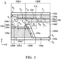
- FIG. 3 illustrates the cross-sectional diagram of a portion of the electronic device 10 in accordance with some other embodiments of the present disclosure. Specifically, FIG. 3 illustrates an enlarged cross-sectional diagram of the region E of the electronic unit 100 shown in FIG. 1 in accordance with some other embodiments of the present disclosure.
- FIG. 3 illustrates an enlarged cross-sectional diagram of the region E of the electronic unit 100 shown in FIG. 1 in accordance with some other embodiments of the present disclosure.
- the embodiment shown in FIG. 3 is similar to the embodiment shown in FIG. 2A .
- the difference between them is that the second insulating structure 108 of the electronic device 10 shown in FIG. 3 also has a greater thickness in a partial region.
- the second insulating structure 108 may be disposed on the second conductive layer 104b and located between the second conductive layer 104b and the modulating material 100M.
- the second insulating structure 108 may include a third insulating layer 108a and a fourth insulating layer 108b disposed on the third insulating layer 108a.
- the material of the third insulating layer 108a may be the same as or different from the material of the fourth insulating layer 108b.
- the thickness of the second insulating structure 108 on the second conductive layer 104b may be varied. More specifically, the thickness of the second insulating structure 108 on the top surface 104b' of the second conductive layer 104b may be varied.
- the second insulating structure 108 may include a third region 108A and a fourth region 108B, and the third region 108A may have a thickness Tc and the fourth region 108B may have a thickness T D .
- the thickness Tc of the third region 108A may be less than the thickness T D of the fourth region 108B, and the fourth region 108B may overlap the second conductive layer 104b.
- the third region 108A may be disposed in the overlapping region OA of the first conductive layer 104a and the second conductive layer 104b, and the fourth region 108B having a greater thickness may be mostly located outside the overlapping region OA or the capacitance adjustable region CA.
- the difference between the thickness Tc of the third region 108A and the thickness T D of the fourth region 108B may be in a range from 0.1 ⁇ m to 3 ⁇ m (i.e. 0.1 ⁇ m ⁇ the thickness T D ⁇ 3 ⁇ m), from 0.5 ⁇ m to 2.5 ⁇ m, or from 1 ⁇ m to 2 ⁇ m.
- the thickness Tc of the third region 108A may be in a range from 0.1 ⁇ m to 3 ⁇ m (i.e. 0.1 ⁇ m ⁇ the thickness T C ⁇ 3 ⁇ m), from 0.5 ⁇ m to 2.5 ⁇ m, or from 1 ⁇ m to 3 ⁇ m.
- the thickness T D of the fourth region 108B may be in a range from 0.1 ⁇ m to 3.5 ⁇ m (i.e. 0.1 ⁇ m ⁇ the thickness T D ⁇ 3 ⁇ m), from 0.5 ⁇ m to 2.5 ⁇ m, from 1 ⁇ m to 3 ⁇ m, or from 1.5 ⁇ m to 3.5 ⁇ m.
- the "thickness" of the third region 108A or the fourth region 108B refers to the maximum thickness of the third region 108A or the fourth region 108B on the top surface 104B' of the second conductive layer 104B in the normal direction of the first substrate 102a or the second substrate 102b (for example, the Z direction shown in the figure).
- the thicknesses of the third insulating layer 108a and the fourth insulating layer 108b described below are also defined in the similar manner.
- the second insulating structure 108 may include the third insulating layer 108a and the fourth insulating layer 108b.
- the third region 108A may include the third insulating layer 108a
- the fourth region 108B may include the third insulating layer 108a and the fourth insulating layer 108b.
- the third region 108A may overlap with the first conductive layer 104a.
- the fourth insulating layer 108b of the fourth region 108B may partially overlap with the second insulating layer 106b of the second region 106B.
- the third insulating layer 108a may have a thickness T 3
- the fourth insulating layer 108b may have a thickness T 4
- the thickness T 4 of the fourth insulating layer 108b may be greater than the thickness T 3 of the third insulating layer 108a.
- the thickness T 3 of the third insulating layer 108a may be in a range from 100 ⁇ to 1500 ⁇ (i.e. 100 ⁇ the thickness T 3 ⁇ 1500 ⁇ ), from 300 ⁇ to 1300 ⁇ , or from 500 ⁇ to 1000 ⁇ , for example, 600 ⁇ , 700 ⁇ , 800 ⁇ , or 900 ⁇ .
- the thickness T 4 of the fourth insulating layer 108b may be in a range from 500 ⁇ to 3000 ⁇ (i.e. 500 ⁇ the thickness T 4 ⁇ 3000 ⁇ ), from 1000 ⁇ to 2500 ⁇ , or from 1500 ⁇ to 2,000 ⁇ , for example, 1600 ⁇ , 1700 ⁇ , 1800 ⁇ , or 1900 ⁇ .
- FIG. 4A and FIG. 4B respectively illustrate the cross-sectional diagram of a portion of the electronic device 10 and the top-view diagram of a portion of the electronic device 10 in accordance with some other embodiments of the present disclosure
- FIG. 4A is the cross-sectional structure along the line segment A-A' in FIG. 4B . It should be understood that only the second conductive layer 104b and the first insulating structure 106 are shown in FIG. 4B and other components are omitted.
- the embodiment shown in FIG. 4A is similar to the embodiment shown in FIG. 2A .
- the difference between them is that the second insulating layer 106b of the electronic device 10 shown in FIG. 4A does not extend into the opening 104p.
- the second insulating layer 106b may be at least partially disposed on the side surface 104s of the first conductive layer 104a that is adjacent to the opening 104p.
- a portion of the second insulating layer 106b may not overlap with the second conductive layer 104b.
- the first region 106A of the first insulating structure 106 may further extend adjacent the opening 104p, and the first region 106A may be adjacent to the opening 104p.
- at least a portion of the first region 106A may be disposed in the overlapping region OA of the first conductive layer 104a and the second conductive layer 104b and the capacitance adjustable region CA.
- the first region 106A may be entirely disposed in the overlapping region OA.
- the first region 106A may have a smaller thickness, and the overlapping region OA of the first conductive layer 104a and the second conductive layer 104b and the capacitance adjustable region CA may at least partially overlap with the first region 106A.
- the stability of the capacitance modulation therefore may be maintained.
- the second region 106B may have a larger thickness and is less likely to generate pinholes during the fabrication process, which may reduce the corrosion of the first conductive layer 104a or reduce the diffusion of metal ions of the first conductive layer 104 into the modulating material 100M.
- FIG. 5 illustrates the cross-sectional diagram of a portion of the electronic device 10 in accordance with some other embodiments of the present disclosure.
- the embodiment shown in FIG. 5 is similar to the embodiment shown in FIG. 4A , except that the second insulating structure 108 of the electronic device 10 shown in FIG. 5 also has a greater thickness in a partial region. That is, the thickness of the second insulating structure 108 may be varied. As shown in FIG. 5 , the second insulating structure 108 may be disposed between the second conductive layer 104b and the modulating material 100M.
- the second insulating structure 108 may include the third insulating layer 108a and the fourth insulating layer 108b disposed on the third insulating layer 108a.
- the second insulating structure 108 in the embodiment shown in FIG. 5 is similar to that of FIG. 3 , and thus will not be repeated herein.
- an insulating structure may have a smaller thickness in the portion corresponding to the capacitance adjustable region, thereby maintaining the stability of the capacitance modulation or improving the operational reliability of the antenna device. Furthermore, in accordance with some embodiments, the insulating structure may have a greater thickness in the portion other than the capacitance adjustable region, thereby the risk of corrosion of the conductive layer or diffusion of metal ions may be reduced.
Landscapes
- Laminated Bodies (AREA)
- Thin Film Transistor (AREA)
- Internal Circuitry In Semiconductor Integrated Circuit Devices (AREA)
Abstract
Description
- This application claims priority of
U.S. Provisional Patent Application No. 62/731,141, filed on September 14, 2018 201910300447.3, filed on April 15, 2019 - The present disclosure relates to an electronic device, and in particular it relates to an antenna having an insulating structure with varied thickness.
- Electronic products that come with a display panel, such as smartphones, tablets, notebooks, monitors, and TVs, have become indispensable necessities in modern society. With the flourishing development of such portable electronic products, consumers have high expectations regarding the quality, functionality, or price of such products. Such electronic products can generally be used as electronic modulation devices as well, for example, as antenna devices that can modulate electromagnetic waves.
- Although currently existing antenna devices have been adequate for their intended purposes, they have not been satisfactory in all respects. The development of an antenna device that can effectively maintain capacitance modulation stability or operational reliability is still one of the goals that the industry currently aims for.
- In accordance with some embodiments of the present disclosure, an antenna device is provided. The antenna device includes a first substrate, a first conductive layer, a first insulating structure, a second substrate, a second conductive layer and a liquid-crystal layer. The first conductive layer is disposed on the first substrate. The first insulating structure is disposed on the first conductive layer, and the first insulating structure includes a first region and a second region. The second substrate is disposed opposite to the first substrate. The second conductive layer is disposed on the second substrate. The liquid-crystal layer is disposed between the first conductive layer and the second conductive layer. The thickness of the first region is less than the thickness of the second region, and at least a portion of the first region is disposed in an overlapping region of the first conductive layer and the second conductive layer.
- A detailed description is given in the following embodiments with reference to the accompanying drawings.
- The disclosure may be more fully understood by reading the subsequent detailed description and examples with references made to the accompanying drawings, wherein:
-
FIG. 1 illustrates the top-view diagram of the electronic device in accordance with some embodiments of the present disclosure; -
FIG. 2A illustrates the cross-sectional diagram of a portion of the electronic device in accordance with some embodiments of the present disclosure; -
FIG. 2B illustrates the top-view diagram of a portion of the electronic device in accordance with some embodiments of the present disclosure; -
FIG. 3 illustrates the cross-sectional diagram of a portion of the electronic device in accordance with some embodiments of the present disclosure; -
FIG. 4A illustrates the cross-sectional diagram of a portion of the electronic device in accordance with some embodiments of the present disclosure; -
FIG. 4B illustrates the top-view diagram of a portion of the electronic device in accordance with some embodiments of the present disclosure; -
FIG. 5 illustrates the cross-sectional diagram of a portion of the electronic device in accordance with some embodiments of the present disclosure. - The structure of the electronic device of the present disclosure and the manufacturing method thereof are described in detail in the following description. In the following detailed description, for purposes of explanation, numerous specific details and embodiments are set forth in order to provide a thorough understanding of the present disclosure. The specific elements and configurations described in the following detailed description are set forth in order to clearly describe the present disclosure. It will be apparent, however, that the exemplary embodiments set forth herein are used merely for the purpose of illustration, and the inventive concept may be embodied in various forms without being limited to those exemplary embodiments. In addition, the drawings of different embodiments may use like and/or corresponding numerals to denote like and/or corresponding elements in order to clearly describe the present disclosure. However, the use of like and/or corresponding numerals in the drawings of different embodiments does not suggest any correlation between different embodiments.
- It should be noted that the elements or devices in the drawings of the present disclosure may be present in any form or configuration known to those with ordinary skill in the art. In addition, in the embodiments, relative expressions are used. For example, "lower", "bottom", "higher" or "top" are used to describe the position of one element relative to another. It should be appreciated that if a device is flipped upside down, an element that is "lower" will become an element that is "higher". It should be understood that the descriptions of the exemplary embodiments are intended to be read in connection with the accompanying drawings, which are to be considered part of the entire written description. The drawings are not drawn to scale. In addition, structures and devices are shown schematically in order to simplify the drawing.
- It should be understood that, although the terms first, second, third etc. may be used herein to describe various elements, components, regions, layers, portions and/or sections, these elements, components, regions, layers, portions and/or sections should not be limited by these terms. These terms are only used to distinguish one element, component, region, layer, portion or section from another region, layer or section. Thus, a first element, component, region, layer, portion or section discussed below could be termed a second element, component, region, layer, portion or section without departing from the teachings of the present disclosure.
- The terms "about" and "substantially" typically mean +/- 20% of the stated value, more typically +/- 10% of the stated value, more typically +/- 5% of the stated value, more typically +/- 3% of the stated value, more typically +/- 2% of the stated value, more typically +/- 1% of the stated value and even more typically +/- 0.5% of the stated value. The stated value of the present disclosure is an approximate value. When there is no specific description, the stated value includes the meaning of "about" or "substantially". Furthermore, the phrase "in a range between a first value and a second value" or "in a range from a first value to a second value" indicates that the range includes the first value, the second value, and other values between them.
- In addition, in some embodiments of the present disclosure, terms concerning attachments, coupling and the like, such as "connected" and "interconnected," refer to a relationship wherein structures are secured or attached to one another either directly or indirectly through intervening structures, as well as both movable or rigid attachments or relationships, unless expressly described otherwise.
- Unless defined otherwise, all technical and scientific terms used herein have the same meaning as commonly understood by one of ordinary skill in the art to which this disclosure belongs. It should be appreciated that, in each case, the term, which is defined in a commonly used dictionary, should be interpreted as having a meaning that conforms to the relative skills of the present disclosure and the background or the context of the present disclosure, and should not be interpreted in an idealized or overly formal manner unless so defined.
- In accordance with some embodiments of the present disclosure, an electronic device (e.g., an antenna device) having an insulating structure with varied thickness is provided. Specifically, in accordance with some embodiments, the insulating structure may have a smaller thickness in a portion corresponding to the capacitance adjustable region, thereby maintaining stability of capacitance modulation or increasing operational reliability of the device. In accordance with some embodiments, the insulating structure may have a greater thickness in a portion other than the capacitance adjustable region, which may reduce the risk of corrosion of the conductive layer or diffusion of metal ions.
- Refer to
FIG. 1 , which illustrates a top-view diagram of anelectronic device 10 in accordance with some embodiments of the present disclosure. It should be understood that only some of the components of theelectronic device 10 are shown inFIG. 1 and other components are omitted for clarity of illustration. The structure of other components will be described in detail in the following figures. In accordance with some embodiments of the present disclosure, additional features may be added to theelectronic device 10 described below. - As shown in
FIG. 1 , theelectronic device 10 may include afirst substrate 102a and a plurality ofelectronic units 100 disposed on thefirst substrate 102a. In accordance with some embodiments, theelectronic device 10 may include an antenna device, a display device (e.g., a liquid-crystal display (LCD)), a light-emitting device, a detecting device, or another device for modulating electromagnetic waves, but it is not limited thereto. In some embodiments, theelectronic device 10 mat be an antenna device, and theelectronic unit 100 may be an antenna unit for modulating electromagnetic waves (e.g., microwaves). It should be understood that the arrangement of theelectronic units 100 is not limited to the aspect shown inFIG. 1 . In accordance with some other embodiments, theelectronic units 100 may be arranged in another suitable manner. - In some embodiments, the material of the
first substrate 102a may include, but is not limited to, glass, quartz, sapphire, ceramic, polyimide (PI), liquid-crystal polymer (LCP) materials, polycarbonate (PC), photo sensitive polyimide (PSPI), polyethylene terephthalate (PET), other suitable substrate materials, or a combination thereof. In some embodiments, thefirst substrate 102a may include a flexible substrate, a rigid substrate, or a combination thereof. - Next, refer to
FIG. 2A , which illustrates a cross-sectional structural diagram of a portion of theelectronic device 10 in accordance with some embodiments of the present disclosure. Specifically,FIG. 2A illustrates an enlarged cross-sectional diagram of a region E of theelectronic unit 100 shown inFIG. 1 in accordance with some embodiments of the present disclosure. As shown inFIG. 2A , theelectronic device 10 may include afirst substrate 102a, asecond substrate 102b, a firstconductive layer 104a, and a secondconductive layer 104b. - The
second substrate 102b may be disposed opposite to thefirst substrate 102a. In some embodiments, the material of thesecond substrate 102b may include, but is not limited to, glass, quartz, sapphire, ceramic, polyimide (PI), liquid-crystal polymer (LCP) materials, polycarbonate (PC), photo-sensitive polyimide (PSPI), polyethylene terephthalate (PET), other suitable substrate materials, or a combination thereof. In some embodiments, thesecond substrate 102b may include a flexible substrate, a rigid substrate, or a combination thereof. In some embodiments, the material of thesecond substrate 102b may be the same as or different from the material of thefirst substrate 102a. - Moreover, the first
conductive layer 104a may be disposed on thefirst substrate 102a. Specifically, the firstconductive layer 104a may be disposed on a first surface S1 of thefirst substrate 102a, and the first surface S1 and a second surface S2 of thefirst substrate 102a are located on opposite sides. In addition, the secondconductive layer 104b may be disposed on thesecond substrate 102b and located between thefirst substrate 102a and thesecond substrate 102b. Specifically, the secondconductive layer 104b may be disposed on the first surface S1 of thesecond substrate 102b, and the first surface S1 of thesecond substrate 102b is adjacent to thefirst substrate 102a. - As shown in
FIG. 2A , in some embodiments, the firstconductive layer 104a may have anopening 104p, and theopening 104p may overlap the secondconductive layer 104b. In accordance with the embodiments of the present disclosure, theopening 104p may be defined as a region that is exposed by the firstconductive layer 104a. That is, theopening 104p may substantially correspond to the region of the first surface S1 of thefirst substrate 102a that is not covered by the firstconductive layer 104a. In addition, the secondconductive layer 104b may overlap the firstconductive layer 104a. In accordance with some embodiments of the present disclosure, the term "overlap" may include partial overlap or entire overlap in the normal direction of thefirst substrate 102a or thesecond substrate 102b (e.g., the Z direction shown in the figure). - Specifically, in some embodiments, the first
conductive layer 104a may be patterned to have anopening 104p. In some embodiments, the secondconductive layer 104b may also be patterned to have multiple regions (only a portion of the secondconductive layer 104b is illustrated in the figure). In some embodiments, multiple regions of the secondconductive layer 104b may be connected to different circuits. - In some embodiments, the second
conductive layer 104b may be electrically connected to a functional circuit (not illustrated). The functional circuit may include active components (e.g., thin film transistors and/or chips) or passive components. In some embodiments, the functional circuit may be located on the first surface S1 of thesecond substrate 102b as the secondconductive layer 104b. In some other embodiments, the functional circuit may be located on the second surface S2 of thesecond substrate 102b, and the functional circuit may be electrically connected to the secondconductive layer 104b, for example, through a via hole (not illustrated) that penetrates thesecond substrate 102b, a flexible circuit board, or another suitable method for electrical connection, but it is not limited thereto. - In some embodiments, the first
conductive layer 104a and the secondconductive layer 104b may include a conductive metal material. In some embodiments, the materials of the firstconductive layer 104a and the secondconductive layer 104b may include, but are not limited to, copper, silver, tin, aluminum, molybdenum, tungsten, gold, chromium, nickel, platinum, copper alloy, silver alloy, tin alloy, aluminum alloy, molybdenum alloy, tungsten alloy, gold alloy, chromium alloy, nickel alloy, platinum alloy, other suitable conductive materials or a combination thereof. - Moreover, the first
conductive layer 104a may have a thickness T', and the secondconductive layer 104b may have a thickness T". In some embodiments, the thickness T' of the firstconductive layer 104a may be in a range from 0.5 micrometers (µm) to 4 micrometers (µm) (i.e. 0.5µm≦the thickness T'≦4µm), from 1.5µm to 3.5µm, or from 2µm to 3µm. In some embodiments, the thickness T" of the secondconductive layer 104b may be in a range from 0.5µm to 4µm (i.e. 0.5µm≦the thickness T"≦4µm), from 1.5µm to 3.5µm, or from 2µm to 3µm. Furthermore, the thickness T' of the firstconductive layer 104a may be the same as or different from the thickness T" of the secondconductive layer 104b. - In accordance with some embodiments of the present disclosure, the "thickness" of the first
conductive layer 104a or the secondconductive layer 104b refers to the maximum thickness of the firstconductive layer 104a or the secondconductive layer 104b in the normal direction of thefirst substrate 102a or thesecond substrate 102b (for example, the Z direction shown in the figure). - In some embodiments, the first
conductive layer 104a and the secondconductive layer 104b may be formed by one or more deposition processes, photolithography processes, or etching processes. In some embodiments, the deposition process may include, but is not limited to, a chemical vapor deposition process, a physical vapor deposition process, an electroplating process, an electroless plating process, other suitable processes, or a combination thereof. The physical vapor deposition process may include, but is not limited to, a sputtering process, an evaporation process, a pulsed laser deposition and so on. In addition, in some embodiments, the photolithography process may include photoresist coating (e.g., spin coating), soft baking, hard baking, mask aligning, exposure, post-exposure baking, developing the photoresist, rinsing, drying, or another suitable process. In some embodiments, the etching process may include a dry etching process, a wet etching process, or another suitable etching process. - Moreover, as shown in
FIG. 2A , theelectronic device 10 may include a firstinsulating structure 106. The firstinsulating structure 106 may be disposed on the firstconductive layer 104a so that the firstconductive layer 104a may be located between thefirst substrate 102a and the firstinsulating structure 106. In addition, the firstinsulating structure 106 may at least partially overlap atop surface 104a' and aside surface 104s of the firstconductive layer 104a. - In some embodiments, the first
insulating structure 106 may have a multi-layered structure. For example, in some embodiments, the firstinsulating structure 106 may include a first insulatinglayer 106a and a second insulatinglayer 106b disposed on the first insulatinglayer 106a, but the present disclosure is not limited thereto. In some embodiments, the second insulatinglayer 106b may expose a portion of the first insulatinglayer 106a. In some other embodiments, the firstinsulating structure 106 may have a single layer structure. - In some embodiments, the
electronic device 10 may further include a secondinsulating structure 108. The secondinsulating structure 108 may be disposed on the secondconductive layer 104b so that the secondconductive layer 104b is located between thesecond substrate 102b and the secondinsulating structure 108. Similarly, the secondinsulating structure 108 may also have a multi-layered structure or a single layer structure. - In addition, as shown in
FIG. 2A , in some embodiments, the firstinsulating structure 106 may at least partially extend on the first surface S1 of thefirst substrate 102a. In other words, the firstinsulating structure 106 may at least partially overlap theopening 104p. In some embodiments, the secondinsulating structure 108 may at least partially extend on the first surface S1 of thesecond substrate 102b. - In some embodiments, the first
insulating structure 106 and the secondinsulating structure 108 may include an insulating material. In some embodiments, the firstinsulating structure 106 and the secondinsulating structure 108 may include, but are not limited to, an organic material, an inorganic material, or a combination thereof. The organic material may include, but is not limited to, polyethylene terephthalate (PET), polyethylene (PE), polyethersulfone (PES), polycarbonate (PC), polymethylmethacrylate (PMMA), polyimide (PI), photo-sensitive polyimide (PSPI) or a combination thereof. The inorganic material may include, but is not limited to, silicon nitride, silicon oxide, silicon oxynitride or a combination thereof. - The material of the first
insulating structure 106 may be the same as or different from the material of the secondinsulating structure 108. In addition, in the embodiments in which the firstinsulating structure 106 or the secondinsulating structure 108 has a multi-layered structure, the materials of the layers may be the same or different. - In some embodiments, the first
insulating structure 106 and the secondinsulating structure 108 may be formed by a chemical vapor deposition process, a sputtering process, a coating process, a printing process, or another suitable process, or a combination thereof. Furthermore, the firstinsulating structure 106 and the secondinsulating structure 108 may be patterned by one or more photolithography processes and etching processes. - In addition, the
electronic device 10 may include a modulatingmaterial 100M disposed between the firstconductive layer 104a and the secondconductive layer 104b. In accordance with some embodiments, a material that can be adjusted to have different properties (e.g., dielectric constants) by applying an electric field or another means can be used as the modulatingmaterial 100M. In some embodiments, the transmission direction of the electromagnetic signals through theopening 104p may be controlled by applying different electric fields to the modulatingmaterial 100M to adjust the capacitance. - In some embodiments, the modulating
material 100M may include, but is not limited to, liquid-crystal molecules (not illustrated) or microelectromechanical systems (MEMS). For example, in some embodiments, theelectronic device 10 may include an electromagnetic element that can be used to emit or receive electromagnetic signals or a MEMS-based antenna unit, but it is not limited thereto. In accordance with some embodiments, the modulatingmaterial 100M may include a liquid-crystal layer. - Specifically, in some embodiments, the functional circuit described above may apply a voltage to the second
conductive layer 104b, and change the properties of the modulatingmaterial 100M between the firstconductive layer 104a and the secondconductive layer 104b by an electric field that is generated between the firstconductive layer 104a and the secondconductive layer 104b. Furthermore, the functional circuit may also apply another voltage to the firstconductive layer 104a, but it is not limited thereto. In some other embodiments, the firstconductive layer 104a may be electrically floating, grounded, or connected to another functional circuit (not illustrated), but it is not limited thereto. - It should be understood that one with ordinary skill in the art may adjust the number, shape or arrangement of the first
conductive layer 104a, the secondconductive layer 104b and thecorresponding opening 104p according to needs, and they are not limited to the aspect illustrated in the figure. - In addition, as shown in
FIG. 2A , the thickness of the firstinsulating structure 106 on the firstconductive layer 104a may be varied in accordance with some embodiments. More specifically, in some embodiments, the thickness of the firstinsulating structure 106 on thetop surface 104a' of the firstconductive layer 104a may be varied. In some embodiments, the firstinsulating structure 106 may include afirst region 106A and asecond region 106B. Thefirst region 106A may have a thickness TA and thesecond region 106B may have a thickness TB. In some embodiments, the thickness TA of thefirst region 106A may be less than a thickness TB of thesecond region 106B, and at least a portion of thefirst region 106A may be disposed in an overlapping region OA of the firstconductive layer 104a and the secondconductive layer 104b. In some embodiments, thefirst region 106A may be entirely disposed in the overlapping region OA. - In some embodiments, the difference between the thickness TB of the
second region 106B and the thickness TA of thefirst region 106A may be in a range from 0.1µm to 3µm (i.e. 0.1µm≦the thickness TA≦3µm), from 0.5µm to 2.5µm, or from 1µm to 2µm. It should be noted that if the difference between the thickness TA and the thickness TB is too large (for example, greater than 3µm), the thicker insulating structure may affect the cell gap of the electronic device, thereby affecting the ability of the capacitance modulation. On the contrary, if the difference between TA and thickness TB is too small (for example, less than 0.1µm), the ability to maintain the stability of capacitance modulation may not be significant. - It should be understood that, in accordance with some embodiments of the present disclosure, "the overlapping region OA of the first
conductive layer 104a and the secondconductive layer 104b" refers to the overlapping region of thebottom surface 104a" of the firstconductive layer 104a and thetop surface 104b' of the secondconductive layer 104b in the normal direction of thefirst substrate 102a or thesecond substrate 102b (for example, the Z direction shown in the figure). - In addition, in accordance with some embodiments of the present disclosure, the "thickness" of the
first region 106A or thesecond region 106B refers to the maximum thickness of thefirst region 106A or thesecond region 106B on thetop surface 104a' of the firstconductive layer 104a in the normal direction of thefirst substrate 102a or thesecond substrate 102b (for example, the Z direction shown in the figure). In addition, the thicknesses of the first insulatinglayer 106a and the second insulatinglayer 106b described below are also defined in the similar manner. Furthermore, in accordance with the embodiments of the present disclosure, the thickness of each component may be measured by using an optical microscopy (OM), a scanning electron microscope (SEM), a film thickness profiler (a-step), an ellipsometer, or another suitable method. Specifically, in some embodiments, after the modulatingmaterial 100M is removed, a cross-sectional image of the structure can be taken using a scanning electron microscope, and the thickness of each component in the above image can be measured. Moreover, the maximum thickness as described above may be the maximum thickness in any cross-sectional image. In other words, the maximum thickness as described above may be the maximum thickness in a partial region of theelectronic device 10. - In accordance with some embodiments, the overlapping region OA may substantially define a capacitance adjustable region CA. Referring to
FIG. 2B at the same time,FIG. 2B illustrates the top-view diagram of a portion of theelectronic device 10 in accordance with some embodiments of the present disclosure, andFIG. 2A is the cross-sectional structure along the line segment A-A' inFIG. 2B . It should be understood that only the secondconductive layer 104b and the firstinsulating structure 106 are shown inFIG. 2B and other components are omitted in order to clearly illustrate the relationship between the overlapping region OA and the capacitance adjustable region CA. - Specifically, the first
conductive layer 104a and the secondconductive layer 104b and the modulatingmaterial 100M located therebetween may form a capacitor structure. The capacitance adjustable region CA of the capacitor structure may substantially correspond to the overlapping region OA and overlap with the overlapping region OA. However, the area where the electromagnetic signal is actually affected by the capacitance will be larger than the overlapping area OA. In accordance with some embodiments, the capacitance adjustable region CA is defined as an area extending outward from the edge of the overlapping region OA by a first distance di. In some embodiments, the first distance d1 may be about 1 mm. - As described above, in some embodiments, the first
insulating structure 106 may include the first insulatinglayer 106a and the second insulatinglayer 106b. In some embodiments, thefirst region 106A may include the first insulatinglayer 106a, and thesecond region 106B may include the first insulatinglayer 106a and the second insulatinglayer 106b. As shown inFIGs. 2A and 2B , in some embodiments, thesecond region 106B may surround thefirst region 106A, and thesecond region 106B may be adjacent to theopening 104p. Moreover, in some embodiments, thefirst region 106A and the secondconductive layer 104b at least partially overlap. - Specifically, the first insulating
layer 106a may have a thickness T1, and the second insulatinglayer 106b may have a thickness T2. In some embodiments, the thickness T2 of the second insulatinglayer 106b may be greater than the thickness T1 of the first insulatinglayer 106a. In some embodiments, the thickness T1 of the first insulatinglayer 106a may be in a range from 100 angstroms (Å) to 1500 angstroms (Å) (i.e. 100Å≦the thickness T1≦1500Å), from 300Å to 1300Å, or from 500Å to 1000Å, for example, 600Å, 700Å, 800Å, or 900Å. In some embodiments, the thickness T2 of the second insulatinglayer 106b may be in a range from 500Å to 3,000Å (i.e. 500Å≦the thickness T2≦3000Å), from 1000Å to 2500Å, or from 1500Å to 2,000Å, for example, 1600Å, 1700Å, 1800Å, or 1900Å. - As described above, the
first region 106A may have a smaller thickness, and the overlapping region OA of the firstconductive layer 104a and the secondconductive layer 104b may at least partially overlap with thefirst region 106A so that the capacitance adjustable region CA may at least partially overlap with thefirst region 106A. With such a configuration, the dielectric loss of the electromagnetic signals may be reduced, or the stability of the capacitance modulation can be maintained. - On the other hand, the
second region 106B may have a greater thickness, and is less likely to generate pinholes during the fabrication process, which may reduce the corrosion of the firstconductive layer 104a or reduce the diffusion of metal ions of the first conductive layer 104 into the modulatingmaterial 100M. In addition, since thesecond region 106B having a greater thickness is mostly located outside the capacitance adjustable region CA, it may have little effect on the dielectric loss of the electromagnetic signals. - In addition, in accordance with some embodiments, alignment layers (not illustrated) may be further disposed between the first
insulating structure 106 and the modulatingmaterial 100M, and between the secondinsulating structure 108 and the modulatingmaterial 100M to control the alignment direction of the liquid-crystal molecules in the modulatingmaterial 100M. In some embodiments, the material of the alignment layer may include, but is not limited to, an organic material, an inorganic material, or a combination thereof. For example, the organic material may include, but is not limited to, polyimide (PI), a photo-reactive polymer material, or a combination thereof. The inorganic material may include, for example, silicon oxide (SiO2), but it is not limited thereto. - In accordance with some embodiments, a buffer layer (not illustrated) may be further disposed between the
first substrate 102a and the firstconductive layer 104a, and between thesecond substrate 102b and the secondconductive layer 104b, so that the expansion coefficient of thefirst substrate 102a and the firstconductive layer 104a and/or the expansion coefficient of thesecond substrate 102b and the secondconductive layer 104b may be matched. In some embodiments, the material of the buffer layer may include, but is not limited to, an organic insulating material, an inorganic insulating material, a metal material, or a combination thereof. - The organic insulating material may include, but is not limited to, an organic compound of acrylic acid or methacrylic acid, an isoprene compound, a phenolformaldehyde resin, benzocyclobutene (BCB), perfluorocyclobutane (PECB), polyimide, polyethylene terephthalate (PET), or a combination thereof. The inorganic material may include, but is not limited to, silicon nitride, silicon oxide, silicon oxynitride or a combination thereof. The metal material may include, but is not limited to, titanium, molybdenum, tungsten, nickel, aluminum, gold, chromium, platinum, silver, copper, titanium alloy, molybdenum alloy, tungsten alloy, nickel alloy, aluminum alloy, gold alloy, chromium alloy, platinum alloy, silver alloy, copper alloy, another suitable material, or a combination thereof.
- In addition, in accordance with some embodiments, the
electronic device 10 may further include a spacer element (not illustrated) disposed between thefirst substrate 102a and thesecond substrate 102b. The spacer element may be disposed in the modulatingmaterial 100M to enhance the structural strength of theelectronic device 10. In some embodiments, the spacer elements may have a ring-shaped structure. In some embodiments, the spacer elements may have columnar structures that are arranged in parallel. - In addition, the spacer element may include an insulating material or a conductive material, or a combination thereof. In some embodiments, the conductive material may include, but is not limited to, copper, silver, gold, copper alloy, silver alloy, gold alloy, or a combination thereof. In some other embodiments, the insulating material may include, but is not limited to, polyethylene terephthalate (PET), polyethylene (PE), polyethersulfone (PES), polycarbonate (PC), polymethylmethacrylate (PMMA), glass or a combination thereof.
- Next, refer to
FIG. 3 , which illustrates the cross-sectional diagram of a portion of theelectronic device 10 in accordance with some other embodiments of the present disclosure. Specifically,FIG. 3 illustrates an enlarged cross-sectional diagram of the region E of theelectronic unit 100 shown inFIG. 1 in accordance with some other embodiments of the present disclosure. It should be understood that the same or similar components or elements in above and below contexts are represented by the same or similar reference numerals. The materials, manufacturing methods and functions of these components or elements are the same or similar to those described above, and thus will not be repeated herein. - The embodiment shown in
FIG. 3 is similar to the embodiment shown inFIG. 2A . The difference between them is that the secondinsulating structure 108 of theelectronic device 10 shown inFIG. 3 also has a greater thickness in a partial region. As shown inFIG. 3 , the secondinsulating structure 108 may be disposed on the secondconductive layer 104b and located between the secondconductive layer 104b and the modulatingmaterial 100M. In this embodiment, the secondinsulating structure 108 may include a third insulating layer 108a and a fourth insulating layer 108b disposed on the third insulating layer 108a. The material of the third insulating layer 108a may be the same as or different from the material of the fourth insulating layer 108b. - As shown in
FIG. 3 , the thickness of the secondinsulating structure 108 on the secondconductive layer 104b may be varied. More specifically, the thickness of the secondinsulating structure 108 on thetop surface 104b' of the secondconductive layer 104b may be varied. In this embodiment, the secondinsulating structure 108 may include athird region 108A and afourth region 108B, and thethird region 108A may have a thickness Tc and thefourth region 108B may have a thickness TD. In some embodiments, the thickness Tc of thethird region 108A may be less than the thickness TD of thefourth region 108B, and thefourth region 108B may overlap the secondconductive layer 104b. - Furthermore, in some embodiments, at least a portion of the
third region 108A may be disposed in the overlapping region OA of the firstconductive layer 104a and the secondconductive layer 104b, and thefourth region 108B having a greater thickness may be mostly located outside the overlapping region OA or the capacitance adjustable region CA. In some embodiments, the difference between the thickness Tc of thethird region 108A and the thickness TD of thefourth region 108B may be in a range from 0.1µm to 3µm (i.e. 0.1µm≦the thickness TD≦3µm), from 0.5µm to 2.5µm, or from 1µm to 2µm. In some embodiments, the thickness Tc of thethird region 108A may be in a range from 0.1µm to 3µm (i.e. 0.1µm≦the thickness TC≦3µm), from 0.5µm to 2.5µm, or from 1µm to 3µm. In some embodiments, the thickness TD of thefourth region 108B may be in a range from 0.1µm to 3.5µm (i.e. 0.1µm≦the thickness TD≦3µm), from 0.5µm to 2.5µm, from 1µm to 3µm, or from 1.5µm to 3.5µm. - Moreover, in accordance with some embodiments of the present disclosure, the "thickness" of the
third region 108A or thefourth region 108B refers to the maximum thickness of thethird region 108A or thefourth region 108B on the top surface 104B' of the second conductive layer 104B in the normal direction of thefirst substrate 102a or thesecond substrate 102b (for example, the Z direction shown in the figure). In addition, the thicknesses of the third insulating layer 108a and the fourth insulating layer 108b described below are also defined in the similar manner. - As described above, in some embodiments, the second
insulating structure 108 may include the third insulating layer 108a and the fourth insulating layer 108b. In some embodiments, thethird region 108A may include the third insulating layer 108a, and thefourth region 108B may include the third insulating layer 108a and the fourth insulating layer 108b. In some embodiments, thethird region 108A may overlap with the firstconductive layer 104a. In some embodiments, the fourth insulating layer 108b of thefourth region 108B may partially overlap with the second insulatinglayer 106b of thesecond region 106B. - In addition, the third insulating layer 108a may have a thickness T3, and the fourth insulating layer 108b may have a thickness T4. In some embodiments, the thickness T4 of the fourth insulating layer 108b may be greater than the thickness T3 of the third insulating layer 108a. In some embodiments, the thickness T3 of the third insulating layer 108a may be in a range from 100Å to 1500Å (i.e. 100Å≦the thickness T3≦1500Å), from 300Å to 1300Å, or from 500Å to 1000Å, for example, 600Å, 700Å, 800Å, or 900Å. In some embodiments, the thickness T4 of the fourth insulating layer 108b may be in a range from 500Å to 3000Å (i.e. 500Å≦the thickness T4≦3000Å), from 1000Å to 2500Å, or from 1500Å to 2,000Å, for example, 1600Å, 1700Å, 1800Å, or 1900Å.
- Next, refer to
FIG. 4A and FIG. 4B , which respectively illustrate the cross-sectional diagram of a portion of theelectronic device 10 and the top-view diagram of a portion of theelectronic device 10 in accordance with some other embodiments of the present disclosure, andFIG. 4A is the cross-sectional structure along the line segment A-A' inFIG. 4B . It should be understood that only the secondconductive layer 104b and the firstinsulating structure 106 are shown inFIG. 4B and other components are omitted. - The embodiment shown in
FIG. 4A is similar to the embodiment shown inFIG. 2A . The difference between them is that the second insulatinglayer 106b of theelectronic device 10 shown inFIG. 4A does not extend into theopening 104p. Specifically, in this embodiment, the second insulatinglayer 106b may be at least partially disposed on theside surface 104s of the firstconductive layer 104a that is adjacent to theopening 104p. Furthermore, as shown inFIGs. 4A and 4B , in some embodiments, a portion of the second insulatinglayer 106b may not overlap with the secondconductive layer 104b. - In this embodiment, the
first region 106A of the firstinsulating structure 106 may further extend adjacent theopening 104p, and thefirst region 106A may be adjacent to theopening 104p. In addition, at least a portion of thefirst region 106A may be disposed in the overlapping region OA of the firstconductive layer 104a and the secondconductive layer 104b and the capacitance adjustable region CA. In some embodiments, thefirst region 106A may be entirely disposed in the overlapping region OA. - As described above, the
first region 106A may have a smaller thickness, and the overlapping region OA of the firstconductive layer 104a and the secondconductive layer 104b and the capacitance adjustable region CA may at least partially overlap with thefirst region 106A. The stability of the capacitance modulation therefore may be maintained. On the other hand, thesecond region 106B may have a larger thickness and is less likely to generate pinholes during the fabrication process, which may reduce the corrosion of the firstconductive layer 104a or reduce the diffusion of metal ions of the first conductive layer 104 into the modulatingmaterial 100M. - Next, refer to
FIG. 5 , which illustrates the cross-sectional diagram of a portion of theelectronic device 10 in accordance with some other embodiments of the present disclosure. The embodiment shown inFIG. 5 is similar to the embodiment shown inFIG. 4A , except that the secondinsulating structure 108 of theelectronic device 10 shown inFIG. 5 also has a greater thickness in a partial region. That is, the thickness of the secondinsulating structure 108 may be varied. As shown inFIG. 5 , the secondinsulating structure 108 may be disposed between the secondconductive layer 104b and the modulatingmaterial 100M. In this embodiment, the secondinsulating structure 108 may include the third insulating layer 108a and the fourth insulating layer 108b disposed on the third insulating layer 108a. The secondinsulating structure 108 in the embodiment shown inFIG. 5 is similar to that ofFIG. 3 , and thus will not be repeated herein. - To summarize the above, in the antenna device provided by the embodiments of the present disclosure, an insulating structure may have a smaller thickness in the portion corresponding to the capacitance adjustable region, thereby maintaining the stability of the capacitance modulation or improving the operational reliability of the antenna device. Furthermore, in accordance with some embodiments, the insulating structure may have a greater thickness in the portion other than the capacitance adjustable region, thereby the risk of corrosion of the conductive layer or diffusion of metal ions may be reduced.
- Although some embodiments of the present disclosure and their advantages have been described in detail, it should be understood that various changes, substitutions and alterations can be made herein without departing from the spirit and scope of the disclosure as defined by the appended claims. For example, it will be readily understood by one of ordinary skill in the art that many of the features, functions, processes, and materials described herein may be varied while remaining within the scope of the present disclosure. In addition, the features of the various embodiments can be used in any combination as long as they do not depart from the spirit and scope of the present disclosure. Moreover, the scope of the present application is not intended to be limited to the particular embodiments of the process, machine, manufacture, composition of matter, means, methods and steps described in the specification. As one of ordinary skill in the art will readily appreciate from the present disclosure, processes, machines, manufacture, compositions of matter, means, methods, or steps, presently existing or later to be developed, that perform substantially the same function or achieve substantially the same result as the corresponding embodiments described herein may be utilized according to the present disclosure. Accordingly, the appended claims are intended to include within their scope such processes, machines, manufacture, compositions of matter, means, methods, or steps.
Claims (15)
- An antenna device, comprising
a first substrate (102a);
a first conductive layer (104a) disposed on the first substrate;
a first insulating structure (106) disposed on the first conductive layer, the first insulating structure comprising a first region (106A) and a second region (106B);
a second substrate (102b) disposed opposite to the first substrate;
a second conductive layer (104b) disposed on the second substrate; and
a liquid-crystal layer (100M) disposed between the first conductive layer and the second conductive layer;
wherein a thickness (TA) of the first region is less than a thickness (TB) of the second region, and at least a portion of the first region is disposed in an overlapping region (OA) of the first conductive layer and the second conductive layer. - The antenna device as claimed in claim 1, wherein the overlapping region defines a capacitance adjustable region (CA) and wherein the capacitance adjustable region overlaps with the overlapping region.
- The antenna device as claimed in claim 1 or 2, wherein the first insulating structure (106) comprises a first insulating layer (106a) and a second insulating layer (106b) disposed on the first insulating layer, and a thickness (T2) of the second insulating layer is greater than a thickness (T1) of the first insulating layer and
wherein the first region comprises the first insulating layer, and the second region comprises the first insulating layer and the second insulating layer. - The antenna device as claimed in claim 3, wherein the second insulating layer exposes a portion of the first insulating layer.
- The antenna device as claimed in any of the claims 1 to 4, wherein the first insulating structure at least partially extends on a first surface of the first substrate.
- The antenna device as claimed in any of the claims 1 to 5, wherein a difference between a thickness of the second region and a thickness of the first region is in a range from 0.1 micrometers to 3 micrometers.
- The antenna device as claimed in claim 1, wherein the first insulating structure comprises a first insulating layer (106a) and a second insulating layer (106b) disposed on the first insulating layer, and the first insulating layer has a thickness in a range from 100 angstroms to 1500 angstroms and
wherein the second insulating layer has a thickness in a range from 500 angstroms to 3000 angstroms. - The antenna device as claimed in any of the claims 1 to 7, wherein a thickness of the first conductive layer is in a range from 0.5 micrometers to 4 micrometers.
- The antenna device as claimed in any of the claims 3 to 8, further comprising a second insulating structure (108) disposed on the second conductive layer, and the second insulating structure comprising a third region (108A) and a fourth region (108B), wherein a thickness (Tc) of the third region is less than a thickness (TD) of the fourth region, and the fourth region overlaps the second conductive layer and
wherein at least a portion of the third region is disposed in the overlapping region. - The antenna device as claimed in claim 9, wherein a difference between the thickness of the third region and the thickness of the fourth region is in a range from 0.1 micrometers to 3 micrometers.
- The antenna device as claimed in claim 9 or 10, wherein the second insulating structure comprises a third insulating layer (108a) and a fourth insulating layer (108b) disposed on the third insulating layer, and a thickness (T4) of the fourth insulating layer is greater than a thickness (T3) of the third insulating layer.
- The antenna device as claimed in claim 11, wherein the fourth insulating layer partially overlaps with the second insulating layer.
- The antenna device as claimed in claim 11 or 12, wherein the thickness of the third insulating layer is in a range from 100 angstroms to 1500 angstroms.
- The antenna device as claimed in any of the claims 1 to 13, wherein the second region surrounds the first region.
- The antenna device as claimed in any of the claims 1 to 14, wherein the first conductive layer has an opening (104p) and the opening overlaps the second conductive layer, and wherein the second region is adjacent to the opening.
Applications Claiming Priority (2)
| Application Number | Priority Date | Filing Date | Title |
|---|---|---|---|
| US201862731141P | 2018-09-14 | 2018-09-14 | |
| CN201910300447.3A CN110911382B (en) | 2018-09-14 | 2019-04-15 | Antenna device |
Publications (2)
| Publication Number | Publication Date |
|---|---|
| EP3624267A1 true EP3624267A1 (en) | 2020-03-18 |
| EP3624267B1 EP3624267B1 (en) | 2023-08-09 |
Family
ID=67874405
Family Applications (1)
| Application Number | Title | Priority Date | Filing Date |
|---|---|---|---|
| EP19195749.7A Active EP3624267B1 (en) | 2018-09-14 | 2019-09-05 | Antenna device |
Country Status (2)
| Country | Link |
|---|---|
| US (1) | US11139562B2 (en) |
| EP (1) | EP3624267B1 (en) |
Families Citing this family (2)
| Publication number | Priority date | Publication date | Assignee | Title |
|---|---|---|---|---|
| CN110911382B (en) * | 2018-09-14 | 2021-06-25 | 群创光电股份有限公司 | Antenna device |
| TWI789877B (en) * | 2021-08-19 | 2023-01-11 | 特崴光波導股份有限公司 | Antenna structure |
Citations (2)
| Publication number | Priority date | Publication date | Assignee | Title |
|---|---|---|---|---|
| WO2018016398A1 (en) * | 2016-07-19 | 2018-01-25 | シャープ株式会社 | Liquid crystal panel and scanning antenna |
| US20180026374A1 (en) * | 2016-07-25 | 2018-01-25 | Innolux Corporation | Antenna device |
Family Cites Families (37)
| Publication number | Priority date | Publication date | Assignee | Title |
|---|---|---|---|---|
| JP4932415B2 (en) * | 2006-09-29 | 2012-05-16 | 株式会社半導体エネルギー研究所 | Semiconductor device |
| KR101452204B1 (en) * | 2007-11-05 | 2014-10-21 | 가부시키가이샤 한도오따이 에네루기 켄큐쇼 | Thin film transistor and display device having the thin film transistor |
| JP5525224B2 (en) * | 2008-09-30 | 2014-06-18 | 株式会社半導体エネルギー研究所 | Display device |
| WO2011036981A1 (en) * | 2009-09-24 | 2011-03-31 | Semiconductor Energy Laboratory Co., Ltd. | Semiconductor device |
| CN107195328B (en) * | 2009-10-09 | 2020-11-10 | 株式会社半导体能源研究所 | Shift register, display device and method of driving the same |
| WO2011089844A1 (en) * | 2010-01-24 | 2011-07-28 | Semiconductor Energy Laboratory Co., Ltd. | Display device and manufacturing method thereof |
| TWI732383B (en) * | 2015-02-06 | 2021-07-01 | 日商半導體能源研究所股份有限公司 | Device, manufacturing method thereof, and electronic device |
| DE102016206922A1 (en) * | 2015-05-08 | 2016-11-10 | Semiconductor Energy Laboratory Co., Ltd. | touchscreen |
| JP6986831B2 (en) * | 2015-07-17 | 2021-12-22 | 株式会社半導体エネルギー研究所 | Semiconductor devices and electronic devices |
| US9911861B2 (en) * | 2015-08-03 | 2018-03-06 | Semiconductor Energy Laboratory Co., Ltd. | Semiconductor device, manufacturing method of the same, and electronic device |
| US9905657B2 (en) * | 2016-01-20 | 2018-02-27 | Semiconductor Energy Laboratory Co., Ltd. | Semiconductor device and method for manufacturing semiconductor device |
| JP6861551B2 (en) * | 2016-04-01 | 2021-04-21 | 株式会社半導体エネルギー研究所 | Organometallic complexes, light emitting elements, light emitting devices, electronic devices, and lighting devices |
| WO2017213084A1 (en) * | 2016-06-09 | 2017-12-14 | シャープ株式会社 | Tft substrate, scanning antenna provided with tft substrate, and method for producing tft substrate |
| CN107658547B (en) | 2016-07-25 | 2019-12-10 | 群创光电股份有限公司 | LCD antenna device |
| JP6712320B2 (en) * | 2016-07-27 | 2020-06-17 | シャープ株式会社 | Scanning antenna |
| WO2018020368A1 (en) * | 2016-07-29 | 2018-02-01 | Semiconductor Energy Laboratory Co., Ltd. | Display method, display device, electronic device, non-temporary memory medium, and program |
| WO2018021247A1 (en) * | 2016-07-29 | 2018-02-01 | シャープ株式会社 | Tft substrate, scanning antenna provided with tft substrate and method for producing tft substrate |
| US10678078B2 (en) * | 2016-08-05 | 2020-06-09 | Semiconductor Energy Laboratory Co., Ltd. | Display device and method for manufacturing the display device |
| KR20180037105A (en) * | 2016-10-03 | 2018-04-11 | 가부시키가이샤 한도오따이 에네루기 켄큐쇼 | Display device, display module, and manufacturing method of display device |
| KR20190069465A (en) * | 2016-10-25 | 2019-06-19 | 가부시키가이샤 한도오따이 에네루기 켄큐쇼 | Display device, display module, electronic device, and touch panel input system |
| US10790319B2 (en) * | 2016-10-27 | 2020-09-29 | Sharp Kabushiki Kaisha | TFT substrate, scanning antenna provided with TFT substrate and method for producing TFT substrate |
| KR102490188B1 (en) * | 2016-11-09 | 2023-01-18 | 가부시키가이샤 한도오따이 에네루기 켄큐쇼 | Display device, display module, electronic device, and manufacturing method of display device |
| JP6717970B2 (en) * | 2016-11-09 | 2020-07-08 | シャープ株式会社 | TFT substrate, scanning antenna provided with TFT substrate, and method for manufacturing TFT substrate |
| JP7050460B2 (en) * | 2016-11-22 | 2022-04-08 | 株式会社半導体エネルギー研究所 | Display device |
| US10756118B2 (en) * | 2016-11-30 | 2020-08-25 | Semiconductor Energy Laboratory Co., Ltd. | Display device, display module, and electronic device |
| WO2018105520A1 (en) * | 2016-12-08 | 2018-06-14 | シャープ株式会社 | Tft substrate, scanning antenna comprising tft substrate, and tft substrate production method |
| CN110050351B (en) * | 2016-12-09 | 2022-06-10 | 夏普株式会社 | TFT substrate, scanning antenna provided with TFT substrate, and method for manufacturing TFT substrate |
| US10992040B2 (en) * | 2016-12-28 | 2021-04-27 | Sharp Kabushiki Kaisha | TFT substrate, scanning antenna comprising TFT substrate, and method for producing TFT substrate |
| CN110100203B (en) * | 2017-01-11 | 2023-04-21 | 株式会社半导体能源研究所 | Display device |
| CN110178170B (en) * | 2017-01-16 | 2021-12-07 | 株式会社半导体能源研究所 | Display device |
| US11509918B2 (en) * | 2017-01-26 | 2022-11-22 | Semiconductor Energy Laboratory Co., Ltd. | Semiconductor device, and electronic device |
| US10608017B2 (en) * | 2017-01-31 | 2020-03-31 | Semiconductor Energy Laboratory Co., Ltd. | Display device, display module, and electronic device |
| US10833422B2 (en) * | 2017-03-03 | 2020-11-10 | Sharp Kabushiki Kaisha | TFT substrate and scanning antenna provided with TFT substrate |
| WO2018186281A1 (en) * | 2017-04-06 | 2018-10-11 | シャープ株式会社 | Tft substrate, and scanning antenna provided with tft substrate |
| CN110462842B (en) * | 2017-04-07 | 2022-05-17 | 夏普株式会社 | TFT substrate, scanning antenna including TFT substrate, and method of manufacturing TFT substrate |
| US10937812B2 (en) * | 2017-04-07 | 2021-03-02 | Sharp Kabushiki Kaisha | TFT substrate, scanning antenna provided with TFT substrate, and method for producing TFT substrate |
| KR102824388B1 (en) * | 2017-05-19 | 2025-06-23 | 가부시키가이샤 한도오따이 에네루기 켄큐쇼 | Semiconductor device, display device, and method for manufacturing semiconductor device |
-
2019
- 2019-08-21 US US16/546,504 patent/US11139562B2/en active Active
- 2019-09-05 EP EP19195749.7A patent/EP3624267B1/en active Active
Patent Citations (2)
| Publication number | Priority date | Publication date | Assignee | Title |
|---|---|---|---|---|
| WO2018016398A1 (en) * | 2016-07-19 | 2018-01-25 | シャープ株式会社 | Liquid crystal panel and scanning antenna |
| US20180026374A1 (en) * | 2016-07-25 | 2018-01-25 | Innolux Corporation | Antenna device |
Also Published As
| Publication number | Publication date |
|---|---|
| US11139562B2 (en) | 2021-10-05 |
| US20200091594A1 (en) | 2020-03-19 |
| EP3624267B1 (en) | 2023-08-09 |
Similar Documents
| Publication | Publication Date | Title |
|---|---|---|
| US20100225869A1 (en) | Liquid crystal display and fabricating method thereof | |
| CN100411193C (en) | Manufacturing method of thin film transistor array panel | |
| CN112505971B (en) | Electronic device and method of manufacturing the same | |
| US7029727B1 (en) | Patterned substrate and liquid crystal display provided therewith | |
| US12266852B2 (en) | Electronic device | |
| EP3624267B1 (en) | Antenna device | |
| KR101593538B1 (en) | Method of making tft substrate and tft substrate thereof | |
| EP3624266B1 (en) | Antenna device | |
| KR102706722B1 (en) | Antenna device | |
| US20240006127A1 (en) | Electronic modulating device including different cell gaps | |
| KR102764833B1 (en) | Electronic device | |
| US7538399B2 (en) | Thin film transistor substrate and manufacturing method thereof | |
| US11953769B2 (en) | Electronic modulating device | |
| US20140168558A1 (en) | Tft array substrate and liquid crystal display | |
| CN111509353B (en) | Electronic device and antenna device | |
| US11798875B2 (en) | Electronic device and manufacturing method thereof | |
| KR20060067486A (en) | Manufacturing Method of Thin Film Transistor Substrate and Thin Film Transistor Substrate |
Legal Events
| Date | Code | Title | Description |
|---|---|---|---|
| PUAI | Public reference made under article 153(3) epc to a published international application that has entered the european phase |
Free format text: ORIGINAL CODE: 0009012 |
|
| STAA | Information on the status of an ep patent application or granted ep patent |
Free format text: STATUS: THE APPLICATION HAS BEEN PUBLISHED |
|
| AK | Designated contracting states |
Kind code of ref document: A1 Designated state(s): AL AT BE BG CH CY CZ DE DK EE ES FI FR GB GR HR HU IE IS IT LI LT LU LV MC MK MT NL NO PL PT RO RS SE SI SK SM TR |
|
| AX | Request for extension of the european patent |
Extension state: BA ME |
|
| STAA | Information on the status of an ep patent application or granted ep patent |
Free format text: STATUS: REQUEST FOR EXAMINATION WAS MADE |
|
| 17P | Request for examination filed |
Effective date: 20200918 |
|
| RBV | Designated contracting states (corrected) |
Designated state(s): AL AT BE BG CH CY CZ DE DK EE ES FI FR GB GR HR HU IE IS IT LI LT LU LV MC MK MT NL NO PL PT RO RS SE SI SK SM TR |
|
| STAA | Information on the status of an ep patent application or granted ep patent |
Free format text: STATUS: EXAMINATION IS IN PROGRESS |
|
| 17Q | First examination report despatched |
Effective date: 20211028 |
|
| GRAP | Despatch of communication of intention to grant a patent |
Free format text: ORIGINAL CODE: EPIDOSNIGR1 |
|
| STAA | Information on the status of an ep patent application or granted ep patent |
Free format text: STATUS: GRANT OF PATENT IS INTENDED |
|
| INTG | Intention to grant announced |
Effective date: 20230306 |
|
| RAP3 | Party data changed (applicant data changed or rights of an application transferred) |
Owner name: INNOLUX CORPORATION |
|
| RIN1 | Information on inventor provided before grant (corrected) |
Inventor name: LI, I-YIN Inventor name: HO, CHIA-CHI Inventor name: HUNG, TANG-CHIN Inventor name: LIN, YI-HUNG |
|
| GRAS | Grant fee paid |
Free format text: ORIGINAL CODE: EPIDOSNIGR3 |
|
| GRAA | (expected) grant |
Free format text: ORIGINAL CODE: 0009210 |
|
| STAA | Information on the status of an ep patent application or granted ep patent |
Free format text: STATUS: THE PATENT HAS BEEN GRANTED |
|
| AK | Designated contracting states |
Kind code of ref document: B1 Designated state(s): AL AT BE BG CH CY CZ DE DK EE ES FI FR GB GR HR HU IE IS IT LI LT LU LV MC MK MT NL NO PL PT RO RS SE SI SK SM TR |
|
| REG | Reference to a national code |
Ref country code: GB Ref legal event code: FG4D |
|
| REG | Reference to a national code |
Ref country code: CH Ref legal event code: EP |
|
| REG | Reference to a national code |
Ref country code: IE Ref legal event code: FG4D |
|
| REG | Reference to a national code |
Ref country code: DE Ref legal event code: R096 Ref document number: 602019034431 Country of ref document: DE |
|
| REG | Reference to a national code |
Ref country code: LT Ref legal event code: MG9D |
|
| REG | Reference to a national code |
Ref country code: NL Ref legal event code: MP Effective date: 20230809 |
|
| REG | Reference to a national code |
Ref country code: AT Ref legal event code: MK05 Ref document number: 1598601 Country of ref document: AT Kind code of ref document: T Effective date: 20230809 |
|
| PG25 | Lapsed in a contracting state [announced via postgrant information from national office to epo] |
Ref country code: GR Free format text: LAPSE BECAUSE OF FAILURE TO SUBMIT A TRANSLATION OF THE DESCRIPTION OR TO PAY THE FEE WITHIN THE PRESCRIBED TIME-LIMIT Effective date: 20231110 |
|
| PG25 | Lapsed in a contracting state [announced via postgrant information from national office to epo] |
Ref country code: IS Free format text: LAPSE BECAUSE OF FAILURE TO SUBMIT A TRANSLATION OF THE DESCRIPTION OR TO PAY THE FEE WITHIN THE PRESCRIBED TIME-LIMIT Effective date: 20231209 |
|
| PG25 | Lapsed in a contracting state [announced via postgrant information from national office to epo] |
Ref country code: SE Free format text: LAPSE BECAUSE OF FAILURE TO SUBMIT A TRANSLATION OF THE DESCRIPTION OR TO PAY THE FEE WITHIN THE PRESCRIBED TIME-LIMIT Effective date: 20230809 Ref country code: RS Free format text: LAPSE BECAUSE OF FAILURE TO SUBMIT A TRANSLATION OF THE DESCRIPTION OR TO PAY THE FEE WITHIN THE PRESCRIBED TIME-LIMIT Effective date: 20230809 Ref country code: PT Free format text: LAPSE BECAUSE OF FAILURE TO SUBMIT A TRANSLATION OF THE DESCRIPTION OR TO PAY THE FEE WITHIN THE PRESCRIBED TIME-LIMIT Effective date: 20231211 Ref country code: NO Free format text: LAPSE BECAUSE OF FAILURE TO SUBMIT A TRANSLATION OF THE DESCRIPTION OR TO PAY THE FEE WITHIN THE PRESCRIBED TIME-LIMIT Effective date: 20231109 Ref country code: NL Free format text: LAPSE BECAUSE OF FAILURE TO SUBMIT A TRANSLATION OF THE DESCRIPTION OR TO PAY THE FEE WITHIN THE PRESCRIBED TIME-LIMIT Effective date: 20230809 Ref country code: LV Free format text: LAPSE BECAUSE OF FAILURE TO SUBMIT A TRANSLATION OF THE DESCRIPTION OR TO PAY THE FEE WITHIN THE PRESCRIBED TIME-LIMIT Effective date: 20230809 Ref country code: LT Free format text: LAPSE BECAUSE OF FAILURE TO SUBMIT A TRANSLATION OF THE DESCRIPTION OR TO PAY THE FEE WITHIN THE PRESCRIBED TIME-LIMIT Effective date: 20230809 Ref country code: IS Free format text: LAPSE BECAUSE OF FAILURE TO SUBMIT A TRANSLATION OF THE DESCRIPTION OR TO PAY THE FEE WITHIN THE PRESCRIBED TIME-LIMIT Effective date: 20231209 Ref country code: HR Free format text: LAPSE BECAUSE OF FAILURE TO SUBMIT A TRANSLATION OF THE DESCRIPTION OR TO PAY THE FEE WITHIN THE PRESCRIBED TIME-LIMIT Effective date: 20230809 Ref country code: GR Free format text: LAPSE BECAUSE OF FAILURE TO SUBMIT A TRANSLATION OF THE DESCRIPTION OR TO PAY THE FEE WITHIN THE PRESCRIBED TIME-LIMIT Effective date: 20231110 Ref country code: FI Free format text: LAPSE BECAUSE OF FAILURE TO SUBMIT A TRANSLATION OF THE DESCRIPTION OR TO PAY THE FEE WITHIN THE PRESCRIBED TIME-LIMIT Effective date: 20230809 Ref country code: AT Free format text: LAPSE BECAUSE OF FAILURE TO SUBMIT A TRANSLATION OF THE DESCRIPTION OR TO PAY THE FEE WITHIN THE PRESCRIBED TIME-LIMIT Effective date: 20230809 |
|
| PG25 | Lapsed in a contracting state [announced via postgrant information from national office to epo] |
Ref country code: PL Free format text: LAPSE BECAUSE OF FAILURE TO SUBMIT A TRANSLATION OF THE DESCRIPTION OR TO PAY THE FEE WITHIN THE PRESCRIBED TIME-LIMIT Effective date: 20230809 |
|
| PG25 | Lapsed in a contracting state [announced via postgrant information from national office to epo] |
Ref country code: ES Free format text: LAPSE BECAUSE OF FAILURE TO SUBMIT A TRANSLATION OF THE DESCRIPTION OR TO PAY THE FEE WITHIN THE PRESCRIBED TIME-LIMIT Effective date: 20230809 |
|
| PG25 | Lapsed in a contracting state [announced via postgrant information from national office to epo] |
Ref country code: SM Free format text: LAPSE BECAUSE OF FAILURE TO SUBMIT A TRANSLATION OF THE DESCRIPTION OR TO PAY THE FEE WITHIN THE PRESCRIBED TIME-LIMIT Effective date: 20230809 Ref country code: RO Free format text: LAPSE BECAUSE OF FAILURE TO SUBMIT A TRANSLATION OF THE DESCRIPTION OR TO PAY THE FEE WITHIN THE PRESCRIBED TIME-LIMIT Effective date: 20230809 Ref country code: ES Free format text: LAPSE BECAUSE OF FAILURE TO SUBMIT A TRANSLATION OF THE DESCRIPTION OR TO PAY THE FEE WITHIN THE PRESCRIBED TIME-LIMIT Effective date: 20230809 Ref country code: EE Free format text: LAPSE BECAUSE OF FAILURE TO SUBMIT A TRANSLATION OF THE DESCRIPTION OR TO PAY THE FEE WITHIN THE PRESCRIBED TIME-LIMIT Effective date: 20230809 Ref country code: DK Free format text: LAPSE BECAUSE OF FAILURE TO SUBMIT A TRANSLATION OF THE DESCRIPTION OR TO PAY THE FEE WITHIN THE PRESCRIBED TIME-LIMIT Effective date: 20230809 Ref country code: CZ Free format text: LAPSE BECAUSE OF FAILURE TO SUBMIT A TRANSLATION OF THE DESCRIPTION OR TO PAY THE FEE WITHIN THE PRESCRIBED TIME-LIMIT Effective date: 20230809 Ref country code: SK Free format text: LAPSE BECAUSE OF FAILURE TO SUBMIT A TRANSLATION OF THE DESCRIPTION OR TO PAY THE FEE WITHIN THE PRESCRIBED TIME-LIMIT Effective date: 20230809 |
|
| REG | Reference to a national code |
Ref country code: CH Ref legal event code: PL |
|
| REG | Reference to a national code |
Ref country code: DE Ref legal event code: R097 Ref document number: 602019034431 Country of ref document: DE |
|
| PG25 | Lapsed in a contracting state [announced via postgrant information from national office to epo] |
Ref country code: LU Free format text: LAPSE BECAUSE OF NON-PAYMENT OF DUE FEES Effective date: 20230905 |
|
| REG | Reference to a national code |
Ref country code: BE Ref legal event code: MM Effective date: 20230930 |
|
| PG25 | Lapsed in a contracting state [announced via postgrant information from national office to epo] |
Ref country code: LU Free format text: LAPSE BECAUSE OF NON-PAYMENT OF DUE FEES Effective date: 20230905 Ref country code: IT Free format text: LAPSE BECAUSE OF FAILURE TO SUBMIT A TRANSLATION OF THE DESCRIPTION OR TO PAY THE FEE WITHIN THE PRESCRIBED TIME-LIMIT Effective date: 20230809 Ref country code: MC Free format text: LAPSE BECAUSE OF FAILURE TO SUBMIT A TRANSLATION OF THE DESCRIPTION OR TO PAY THE FEE WITHIN THE PRESCRIBED TIME-LIMIT Effective date: 20230809 |
|
| PLBE | No opposition filed within time limit |
Free format text: ORIGINAL CODE: 0009261 |
|
| STAA | Information on the status of an ep patent application or granted ep patent |
Free format text: STATUS: NO OPPOSITION FILED WITHIN TIME LIMIT |
|
| REG | Reference to a national code |
Ref country code: IE Ref legal event code: MM4A |
|
| PG25 | Lapsed in a contracting state [announced via postgrant information from national office to epo] |
Ref country code: IE Free format text: LAPSE BECAUSE OF NON-PAYMENT OF DUE FEES Effective date: 20230905 |
|
| 26N | No opposition filed |
Effective date: 20240513 |
|
| PG25 | Lapsed in a contracting state [announced via postgrant information from national office to epo] |
Ref country code: CH Free format text: LAPSE BECAUSE OF NON-PAYMENT OF DUE FEES Effective date: 20230930 |
|
| PG25 | Lapsed in a contracting state [announced via postgrant information from national office to epo] |
Ref country code: IE Free format text: LAPSE BECAUSE OF NON-PAYMENT OF DUE FEES Effective date: 20230905 Ref country code: CH Free format text: LAPSE BECAUSE OF NON-PAYMENT OF DUE FEES Effective date: 20230930 Ref country code: SI Free format text: LAPSE BECAUSE OF FAILURE TO SUBMIT A TRANSLATION OF THE DESCRIPTION OR TO PAY THE FEE WITHIN THE PRESCRIBED TIME-LIMIT Effective date: 20230809 |
|
| PG25 | Lapsed in a contracting state [announced via postgrant information from national office to epo] |
Ref country code: BE Free format text: LAPSE BECAUSE OF NON-PAYMENT OF DUE FEES Effective date: 20230930 |
|
| PG25 | Lapsed in a contracting state [announced via postgrant information from national office to epo] |
Ref country code: BG Free format text: LAPSE BECAUSE OF FAILURE TO SUBMIT A TRANSLATION OF THE DESCRIPTION OR TO PAY THE FEE WITHIN THE PRESCRIBED TIME-LIMIT Effective date: 20230809 |
|
| PG25 | Lapsed in a contracting state [announced via postgrant information from national office to epo] |
Ref country code: BG Free format text: LAPSE BECAUSE OF FAILURE TO SUBMIT A TRANSLATION OF THE DESCRIPTION OR TO PAY THE FEE WITHIN THE PRESCRIBED TIME-LIMIT Effective date: 20230809 |
|
| PG25 | Lapsed in a contracting state [announced via postgrant information from national office to epo] |
Ref country code: CY Free format text: LAPSE BECAUSE OF FAILURE TO SUBMIT A TRANSLATION OF THE DESCRIPTION OR TO PAY THE FEE WITHIN THE PRESCRIBED TIME-LIMIT; INVALID AB INITIO Effective date: 20190905 |
|
| PG25 | Lapsed in a contracting state [announced via postgrant information from national office to epo] |
Ref country code: HU Free format text: LAPSE BECAUSE OF FAILURE TO SUBMIT A TRANSLATION OF THE DESCRIPTION OR TO PAY THE FEE WITHIN THE PRESCRIBED TIME-LIMIT; INVALID AB INITIO Effective date: 20190905 |
|
| PGFP | Annual fee paid to national office [announced via postgrant information from national office to epo] |
Ref country code: DE Payment date: 20250827 Year of fee payment: 7 |
|
| PGFP | Annual fee paid to national office [announced via postgrant information from national office to epo] |
Ref country code: GB Payment date: 20250828 Year of fee payment: 7 |
|
| PGFP | Annual fee paid to national office [announced via postgrant information from national office to epo] |
Ref country code: FR Payment date: 20250908 Year of fee payment: 7 |
|
| PG25 | Lapsed in a contracting state [announced via postgrant information from national office to epo] |
Ref country code: TR Free format text: LAPSE BECAUSE OF FAILURE TO SUBMIT A TRANSLATION OF THE DESCRIPTION OR TO PAY THE FEE WITHIN THE PRESCRIBED TIME-LIMIT Effective date: 20230809 |