EP3624238A2 - Method for surface patterning of lithium metal, and lithium secondary battery electrode using same - Google Patents
Method for surface patterning of lithium metal, and lithium secondary battery electrode using same Download PDFInfo
- Publication number
- EP3624238A2 EP3624238A2 EP18846398.8A EP18846398A EP3624238A2 EP 3624238 A2 EP3624238 A2 EP 3624238A2 EP 18846398 A EP18846398 A EP 18846398A EP 3624238 A2 EP3624238 A2 EP 3624238A2
- Authority
- EP
- European Patent Office
- Prior art keywords
- lithium metal
- patterning
- substrate
- pattern
- lithium
- Prior art date
- Legal status (The legal status is an assumption and is not a legal conclusion. Google has not performed a legal analysis and makes no representation as to the accuracy of the status listed.)
- Granted
Links
Images


Classifications
-
- H—ELECTRICITY
- H01—ELECTRIC ELEMENTS
- H01M—PROCESSES OR MEANS, e.g. BATTERIES, FOR THE DIRECT CONVERSION OF CHEMICAL ENERGY INTO ELECTRICAL ENERGY
- H01M4/00—Electrodes
- H01M4/02—Electrodes composed of, or comprising, active material
- H01M4/04—Processes of manufacture in general
- H01M4/043—Processes of manufacture in general involving compressing or compaction
- H01M4/0435—Rolling or calendering
-
- G—PHYSICS
- G03—PHOTOGRAPHY; CINEMATOGRAPHY; ANALOGOUS TECHNIQUES USING WAVES OTHER THAN OPTICAL WAVES; ELECTROGRAPHY; HOLOGRAPHY
- G03F—PHOTOMECHANICAL PRODUCTION OF TEXTURED OR PATTERNED SURFACES, e.g. FOR PRINTING, FOR PROCESSING OF SEMICONDUCTOR DEVICES; MATERIALS THEREFOR; ORIGINALS THEREFOR; APPARATUS SPECIALLY ADAPTED THEREFOR
- G03F7/00—Photomechanical, e.g. photolithographic, production of textured or patterned surfaces, e.g. printing surfaces; Materials therefor, e.g. comprising photoresists; Apparatus specially adapted therefor
- G03F7/0002—Lithographic processes using patterning methods other than those involving the exposure to radiation, e.g. by stamping
-
- G—PHYSICS
- G03—PHOTOGRAPHY; CINEMATOGRAPHY; ANALOGOUS TECHNIQUES USING WAVES OTHER THAN OPTICAL WAVES; ELECTROGRAPHY; HOLOGRAPHY
- G03F—PHOTOMECHANICAL PRODUCTION OF TEXTURED OR PATTERNED SURFACES, e.g. FOR PRINTING, FOR PROCESSING OF SEMICONDUCTOR DEVICES; MATERIALS THEREFOR; ORIGINALS THEREFOR; APPARATUS SPECIALLY ADAPTED THEREFOR
- G03F7/00—Photomechanical, e.g. photolithographic, production of textured or patterned surfaces, e.g. printing surfaces; Materials therefor, e.g. comprising photoresists; Apparatus specially adapted therefor
- G03F7/20—Exposure; Apparatus therefor
- G03F7/2002—Exposure; Apparatus therefor with visible light or UV light, through an original having an opaque pattern on a transparent support, e.g. film printing, projection printing; by reflection of visible or UV light from an original such as a printed image
- G03F7/2012—Exposure; Apparatus therefor with visible light or UV light, through an original having an opaque pattern on a transparent support, e.g. film printing, projection printing; by reflection of visible or UV light from an original such as a printed image using liquid photohardening compositions, e.g. for the production of reliefs such as flexographic plates or stamps
-
- H—ELECTRICITY
- H01—ELECTRIC ELEMENTS
- H01M—PROCESSES OR MEANS, e.g. BATTERIES, FOR THE DIRECT CONVERSION OF CHEMICAL ENERGY INTO ELECTRICAL ENERGY
- H01M10/00—Secondary cells; Manufacture thereof
- H01M10/05—Accumulators with non-aqueous electrolyte
- H01M10/052—Li-accumulators
-
- H—ELECTRICITY
- H01—ELECTRIC ELEMENTS
- H01M—PROCESSES OR MEANS, e.g. BATTERIES, FOR THE DIRECT CONVERSION OF CHEMICAL ENERGY INTO ELECTRICAL ENERGY
- H01M10/00—Secondary cells; Manufacture thereof
- H01M10/05—Accumulators with non-aqueous electrolyte
- H01M10/052—Li-accumulators
- H01M10/0525—Rocking-chair batteries, i.e. batteries with lithium insertion or intercalation in both electrodes; Lithium-ion batteries
-
- H—ELECTRICITY
- H01—ELECTRIC ELEMENTS
- H01M—PROCESSES OR MEANS, e.g. BATTERIES, FOR THE DIRECT CONVERSION OF CHEMICAL ENERGY INTO ELECTRICAL ENERGY
- H01M4/00—Electrodes
- H01M4/02—Electrodes composed of, or comprising, active material
- H01M4/04—Processes of manufacture in general
- H01M4/0402—Methods of deposition of the material
-
- H—ELECTRICITY
- H01—ELECTRIC ELEMENTS
- H01M—PROCESSES OR MEANS, e.g. BATTERIES, FOR THE DIRECT CONVERSION OF CHEMICAL ENERGY INTO ELECTRICAL ENERGY
- H01M4/00—Electrodes
- H01M4/02—Electrodes composed of, or comprising, active material
- H01M4/04—Processes of manufacture in general
- H01M4/043—Processes of manufacture in general involving compressing or compaction
-
- H—ELECTRICITY
- H01—ELECTRIC ELEMENTS
- H01M—PROCESSES OR MEANS, e.g. BATTERIES, FOR THE DIRECT CONVERSION OF CHEMICAL ENERGY INTO ELECTRICAL ENERGY
- H01M4/00—Electrodes
- H01M4/02—Electrodes composed of, or comprising, active material
- H01M4/04—Processes of manufacture in general
- H01M4/0483—Processes of manufacture in general by methods including the handling of a melt
- H01M4/0485—Casting
-
- H—ELECTRICITY
- H01—ELECTRIC ELEMENTS
- H01M—PROCESSES OR MEANS, e.g. BATTERIES, FOR THE DIRECT CONVERSION OF CHEMICAL ENERGY INTO ELECTRICAL ENERGY
- H01M4/00—Electrodes
- H01M4/02—Electrodes composed of, or comprising, active material
- H01M4/13—Electrodes for accumulators with non-aqueous electrolyte, e.g. for lithium-accumulators; Processes of manufacture thereof
- H01M4/134—Electrodes based on metals, Si or alloys
-
- H—ELECTRICITY
- H01—ELECTRIC ELEMENTS
- H01M—PROCESSES OR MEANS, e.g. BATTERIES, FOR THE DIRECT CONVERSION OF CHEMICAL ENERGY INTO ELECTRICAL ENERGY
- H01M4/00—Electrodes
- H01M4/02—Electrodes composed of, or comprising, active material
- H01M4/13—Electrodes for accumulators with non-aqueous electrolyte, e.g. for lithium-accumulators; Processes of manufacture thereof
- H01M4/139—Processes of manufacture
- H01M4/1395—Processes of manufacture of electrodes based on metals, Si or alloys
-
- H—ELECTRICITY
- H01—ELECTRIC ELEMENTS
- H01M—PROCESSES OR MEANS, e.g. BATTERIES, FOR THE DIRECT CONVERSION OF CHEMICAL ENERGY INTO ELECTRICAL ENERGY
- H01M4/00—Electrodes
- H01M4/02—Electrodes composed of, or comprising, active material
- H01M4/36—Selection of substances as active materials, active masses, active liquids
- H01M4/38—Selection of substances as active materials, active masses, active liquids of elements or alloys
- H01M4/381—Alkaline or alkaline earth metals elements
- H01M4/382—Lithium
-
- H—ELECTRICITY
- H01—ELECTRIC ELEMENTS
- H01M—PROCESSES OR MEANS, e.g. BATTERIES, FOR THE DIRECT CONVERSION OF CHEMICAL ENERGY INTO ELECTRICAL ENERGY
- H01M4/00—Electrodes
- H01M4/02—Electrodes composed of, or comprising, active material
- H01M2004/021—Physical characteristics, e.g. porosity, surface area
-
- H—ELECTRICITY
- H01—ELECTRIC ELEMENTS
- H01M—PROCESSES OR MEANS, e.g. BATTERIES, FOR THE DIRECT CONVERSION OF CHEMICAL ENERGY INTO ELECTRICAL ENERGY
- H01M4/00—Electrodes
- H01M4/02—Electrodes composed of, or comprising, active material
- H01M2004/025—Electrodes composed of, or comprising, active material with shapes other than plane or cylindrical
-
- H—ELECTRICITY
- H01—ELECTRIC ELEMENTS
- H01M—PROCESSES OR MEANS, e.g. BATTERIES, FOR THE DIRECT CONVERSION OF CHEMICAL ENERGY INTO ELECTRICAL ENERGY
- H01M4/00—Electrodes
- H01M4/02—Electrodes composed of, or comprising, active material
- H01M2004/026—Electrodes composed of, or comprising, active material characterised by the polarity
- H01M2004/027—Negative electrodes
-
- Y—GENERAL TAGGING OF NEW TECHNOLOGICAL DEVELOPMENTS; GENERAL TAGGING OF CROSS-SECTIONAL TECHNOLOGIES SPANNING OVER SEVERAL SECTIONS OF THE IPC; TECHNICAL SUBJECTS COVERED BY FORMER USPC CROSS-REFERENCE ART COLLECTIONS [XRACs] AND DIGESTS
- Y02—TECHNOLOGIES OR APPLICATIONS FOR MITIGATION OR ADAPTATION AGAINST CLIMATE CHANGE
- Y02E—REDUCTION OF GREENHOUSE GAS [GHG] EMISSIONS, RELATED TO ENERGY GENERATION, TRANSMISSION OR DISTRIBUTION
- Y02E60/00—Enabling technologies; Technologies with a potential or indirect contribution to GHG emissions mitigation
- Y02E60/10—Energy storage using batteries
Definitions
- the present application claims priority to Korean Patent Application No. 10-2017-0104306 filed on August 17, 2017 and Korean Patent Application No. 10-2017-0104307 filed on August 17, 2017 in the Republic of Korea, the disclosures of which are incorporated herein by reference.
- the present disclosure relates to a method for patterning a lithium metal surface and an electrode for a lithium secondary battery using the same.
- the present disclosure relates to a method for patterning a lithium metal surface by using a patterning substrate having high releasability from lithium metal, and an electrode for a lithium secondary battery using the same.
- lithium metal secondary batteries using lithium metal or a lithium alloy as a negative electrode having high energy density have been given many attentions.
- a lithium metal secondary battery refers to a secondary battery using lithium metal or a lithium alloy as a negative electrode.
- Lithium metal has a low density of 0.54 g/cm 3 and a significantly low standard reduction potential of -3.045V (SHE: based on the standard hydrogen electrode), and thus has been most spotlighted as an electrode material for a high-energy density battery.
- lithium metal When using lithium metal as a negative electrode, lithium metal reacts with an electrolyte, impurities, such as water or an organic solvent, a lithium salt, or the like, to form a solid electrolyte interphase (SEI) layer.
- SEI solid electrolyte interphase
- Such an SEI layer causes a local difference in current density to accelerate formation of resinous dendrite caused by lithium metal during charge. Then, such dendrite grows gradually during charge/discharge to cause an internal short-circuit between a positive electrode and a negative electrode.
- dendrite has a mechanically weak bottle neck portion to form dead lithium, which loses electrical contact with a current collector during discharge. As a result, the capacity of a battery is decreased, the cycle life of a battery is reduced, and the stability of a battery is degraded.
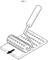
- FIG. 1 illustrates a method for surface treatment of lithium metal using micro-needles.
- the surface treatment of lithium metal using micro-needles can treat a large surface area through simple rolling which can be carried out economically and effectively.
- charge/discharge and cycle characteristics it is possible to improve charge/discharge and cycle characteristics, to reduce interfacial resistance and to inhibit lithium precipitation on the surface of an electrode.
- the micro-needles rotate a roller continuously, processing of the roller is very important.
- the roller surface actually performs elliptical rolling 101, not perfect circular rolling 102 during rolling, and thus the surface may not be treated uniformly.
- Such non-uniform treatment also occurs when the micro-needles processed on the roller surface are not uniform.
- the surface treatment using micro-needles is in a nanometer or micrometer scale, such surface nonuniformity directly results in degradation of the life and performance of a battery.
- the roller is smaller than the conventional lithium metal foil, it is difficult to process lithium metal foil having a large area at once. Thus, it is required to carry out rolling many times for one foil, which may result in non-uniform surface treatment.
- the above-mentioned processing may not be problematic in the case of foil having a small area. However, when commercially available products are produced in a large amount, it may cause a serious problem.
- the present disclosure is directed to providing a method for patterning a lithium metal surface which improves reversibility of lithium metal, allows uniform patterning of lithium metal with a large area as compared to the conventional patterning methods, and particularly uses a patterning substrate having high releasability from lithium metal, and an electrode for a lithium secondary battery using the same.
- a method for patterning a lithium metal surface including the steps of: (S1) forming an intaglio or relief pattern having a predetermined size on a patterning substrate; (S2) compressing lithium metal physically to the surface of the patterning substrate having the pattern formed thereon, or applying liquid lithium thereto and solidifying it to form a predetermined pattern on the surface of lithium metal; and (S3) separating the lithium metal having the predetermined pattern formed thereon from the patterning substrate.
- the method for patterning a lithium metal surface as defined in the first embodiment wherein the patterning substrate is at least one selected from a silicon wafer or polycarbonate substrate.
- the method for patterning a lithium metal surface as defined in the first or the second embodiment wherein the patterning substrate is a silicon wafer, and the method may further include a step of forming a photoresist coating layer on the surface of the silicon wafer having the pattern formed thereon, before carrying out step (S2).
- the patterning substrate is a polycarbonate substrate
- step (S1) may be carried out by preparing a silicon wafer having a relief or intaglio pattern with a predetermined size and compressing the polycarbonate substrate physically thereto to form the polycarbonate substrate having the pattern formed thereon.
- the method for patterning a lithium metal surface as defined in any one of the first to the fifth embodiments wherein the intaglio or relief pattern having a predetermined size may have a depth or height corresponding to 0.01-1 times of the size of the horizontal section of the intaglio or relief pattern having a predetermined size.
- an electrode for a lithium secondary battery which includes patterned lithium metal obtained by the method as described above.
- a predetermined pattern is formed on the surface of lithium metal by compressing lithium metal physically to a patterning substrate having a predetermined pattern, or applying liluid lithium thereto and solidifying it.
- the patterning substrate has high releasability from lithium metal, it is possible to separate lithium metal with ease from the patterning substrate, after the lithium metal surface is patterned.
- the patterning substrate is a silicon wafer
- a photoresist coating layer is formed on the surface of the silicon wafer to increase releasability from lithium metal. Therefore, when lithium metal is separated from the silicon wafer, it is possible to separate lithium metal with ease.
- the patterned lithium metal has higher reversibility as compared to the conventional lithium metal. Thus, it is possible to improve the life of a battery significantly.
- the present disclosure relates a method for providing a negative electrode patterned with a predetermined pattern of intaglio and/or relief, and a negative electrode obtained thereby.
- the negative electrode includes lithium metal as a negative electrode active material.
- lithium metal has low releasability, and thus is easily attached to the surface of another material that is in contact therewith or is not separated completely from the surface of a negative electrode but protrudes out from the surface to form burrs undesirably.
- the present disclosure provides a method for patterning the surface of a negative electrode including lithium metal with low releasability smoothly and uniformly, and a negative electrode obtained thereby.
- a method for patterning a lithium metal surface including the steps of: (S1) forming an intaglio or relief pattern having a predetermined size on a patterning substrate; (S2) compressing lithium metal physically to the surface of the patterning substrate having the pattern formed thereon, or applying liquid lithium thereto and solidifying it to form a predetermined pattern on the surface of lithium metal; and (S3) separating the lithium metal having the predetermined pattern formed thereon from the patterning substrate.
- a predetermined pattern is formed on the surface of lithium metal by compressing lithium metal physically to a patterning substrate having a predetermined pattern, or applying liluid lithium thereto and solidifying it. As a result, it is possible to produce patterned lithium metal foil in a large amount.
- the patterning substrate has high releasability from lithium metal.
- the patterning substrate is at least one selected from a silicon wafer and a polycarbonate substrate.
- the patterning substrate when the patterning substrate is a silicon wafer, it is preferred that the surface of the substrate is totally coated with a photoresist coating layer, wherein the photoresist coating layer is formed with a uniform thickness along the height difference of the pattern formed on the silicon wafer substrate.
- the patterning substrate including a silicon wafer whose surface is coated with a photoresist coating layer may be prepared by the following method.
- the silicon wafer is patterned so that it may have a predetermined patter.
- the patterning may be carried out without any particular limitation, as long as it can be applied to a process for fabricating a semiconductor substrate and allows patterning of the surface of a silicon wafer surface.
- a photolithography process may be used to carry out patterning.
- the photolithography process may include the steps of: preparing a plate-type silicon wafer having no surface pattern and carrying out spin coating of a photoresist layer on the surface thereof; exposing the photoresist layer selectively by using a photomask, or the like; developing the exposed photoresist layer to generate a mask pattern; carrying out etching or doping on the region of the semiconductor substrate not shielded by the photoresist; and carrying out ashing to remove the photoresist pattern used as a mask during the etching and doping step.
- a predetermined pattern is formed on the surface of the silicon wafer through the above-mentioned steps.
- the pattern is not limited to any specific shape or specific range of values.
- the pattern may depend on the design of a battery, such as the purpose of use or application of a battery, and the pattern shape, line width or depth of the intaglio or relief pattern, or the like, may be variable.
- the photoresist coating layer may include a polymer compound which undergoes chemical reaction by the light and electron beams and is used conventionally for a photoresist layer in the field of semiconductors.
- a polymer compound which undergoes chemical reaction by the light and electron beams and is used conventionally for a photoresist layer in the field of semiconductors.
- Particular examples of such a polymer include norbornene/maleic anhydride copolymer, norbornene/maleate copolymer, and methacrylate polymer having a pendant alicyclic structure.
- the photoresist coating layer may include at least one of the above-listed polymers, but is not limited thereto.
- the surface of the silicon wafer is provided with releasability from lithium metal by virtue of the photoresist coating layer. It is important to form a thin and uniform layer depending on the height difference of the pattern so that the resolution of the pattern may not be decreased due to the formation of the coating layer. It is preferred for the photoresist coating layer to have a thickness sufficient for providing the surface with releasability.
- the photoresist coating layer formed on the surface of the silicon wafer increases releasability from lithium metal, it is possible to separate lithium metal easily from the silicon wafer when lithium metal is separated from the silicon wafer.
- the photoresist coating layer may have a thickness of 0.7-1.5 ⁇ m.
- the photoresist coating layer satisfies the above-defined thickness range, it is possible to ensure releasability from lithium metal, while not significantly affecting the size of the pattern formed on the silicon wafer.
- the photoresist coating layer has a thickness less than 0.7 ⁇ m, it cannot be coated well on the patterned silicon wafer, thereby making it difficult to ensure releasability from lithium metal.
- the photoresist coating layer has a thickness larger than 1.5 ⁇ m, it becomes excessively thick to cause deformation of the original shape of the pattern formed on the silicon wafer, thereby making it difficult to form a pattern on lithium metal.
- the patterning substrate may be a polymer substrate.
- the polymer substrate preferably has higher strength as compared to lithium metal in order to form a pattern on the surface of lithium metal through compression, after forming a predetermined pattern on the surface thereof.
- the polymer substrate preferably has high releasability from lithium metal to prevent generation of burrs on the surface of lithium metal after compression, or to prevent lithium metal from being attached to the patterning substrate.
- the polymer substrate may be a polycarbonate substrate including a polycarbonate material. Since polycarbonate has high releasability from lithium metal, lithium metal can be separated with ease when it is separated from the polycarbonate substrate.
- the polycarbonate substrate itself is flexible, it is possible to carry out patterning of lithium metal through a simple rolling process, and it is possible to remove the polycarbonate substrate efficiently from lithium metal after forming a pattern.
- patterning of the polycarbonate substrate may be carried out by using a mold made of a ceramic or metallic material.
- polycarbonate is a flexible material having ductility, it is possible to introduce a predetermined pattern to the polycarbonate substrate by compressing the plate-type polycarbonate substrate against the mold.
- patterning of the polycarbonate substrate may be carried out by melting polycarbonate or dissolving polycarbonate into a desired solvent to form a polymer solution and casting the polymer solution to the mold.
- the mold used herein may be a silicon wafer having the pattern obtained by the above-described method.
- a silicon wafer substrate obtained from the photolithography process may be used to compress the polycarbonate substrate physically so that the polycarbonate substrate may be provided with the pattern.
- the silicon wafer substrate obtained from the photolithography process, there is no need for forming a photoresist coating layer on the surface of the silicon wafer substrate.
- the patterning accords with a desired negative electrode pattern and pattern width or the depth is determined by the purpose of use of a negative electrode or characteristics to be realized, and thus the patterning is not limited to any particular pattern.
- the horizontal section of the intaglio or relief pattern formed on the patterning pattern with a predetermined size may have a size of 10-900 ⁇ m independently.
- the pattern in the case of an intaglio pattern, the pattern may have a depth of 10-20 ⁇ m, but is not limited thereto.
- the negative electrode pattern may have a line width of 10 ⁇ m or more, or 20 ⁇ m, and an interval of 10 ⁇ m or more, or 20 ⁇ m.
- the pattern formed on the patterning substrate may have various shapes and it is possible to form a pattern with a larger area as compared to the conventional roller-type micro-needles.
- the most fundamental pattern may be repeated squares or hexagons (honeycomb structure).
- various polygons, such as triangles, and circular or elliptical shapes, or various geometrical lattice patterns may be formed.
- the depth or height of the intaglio or relief pattern with a predetermined size may correspond to 0.01-1 times of the size of the horizontal section of the intaglio or relief pattern with a predetermined size.
- lithium foil may be disposed on a patterning substrate having an intaglio or relief pattern formed thereon, and then a predetermined level of physical pressure may be applied thereto by using a roller, press, or the like.
- the physical pressure applied to the lithium metal foil may be varied with the thickness of lithium metal foil and the height of intaglio and relief of the patterning substrate.
- the lithium metal foil is separated from the patterning substrate after removing the physical pressure, it is possible to obtain patterned lithium metal finally.
- the patterning substrate is a polycarbonate substrate, polycarbonate has high releasability from lithium metal, and thus it is possible to carry out separation from lithium metal with ease.
- the patterning substrate is a silicon wafer, it is possible to carry out separation from lithium metal with ease by virtue of the photoresist coating layer formed on the surface thereof.
- a lithium secondary battery by using the lithium metal patterned according to the present disclosure.
- a positive electrode, separator and a non-aqueous electrolyte used conventionally for a lithium secondary battery may be used.
- the patterned lithium metal has a larger surface area as compared to non-treated lithium metal.
- the patterned lithium metal provides relatively lower current density to allow stable charge/discharge.
- a lithium metal secondary battery undergoes charge/discharge, while lithium is intercalated/deintercalated to/from the lithium metal surface.
- lithium metal is grown non-ideally and deintercalation of the corresponding portion causes degradation of the reversibility of a cell and adversely affects the stability of a cell.
- the patterned lithium metal according to the present disclosure has an increased surface area and provides relatively lower current density, thereby inhibiting non-ideal growth of lithium metal. Thus, it is possible to improve the overall performance of a battery, which becomes significant as charge/discharge cycles are repeated.
- the patterned lithium metal according to the present disclosure can be obtained uniformly with a larger area as compared to the conventional patterning using micro-needles. In addition, there is no problem caused by a difference in pressure during rolling. Further, it is possible to carry out patterning with a large area. Thus, the patterned lithium metal according to the present disclosure can be applied actually to a commercially available process.
- the patterning substrate is a silicon wafer
- a micropatterned silicon wafer having a width of 100 ⁇ m, a length of 100 ⁇ m and a height of 17 ⁇ m was coated with a photoresist coating layer.
- FIG. 3 is a scanning electron microscopic (SEM) image illustrating the surface of a silicon wafer having a photoresist coating layer formed thereon according to an embodiment of the present disclosure.
- the photoresist coating layer had a thickness of 1.0 ⁇ m. Then, lithium metal was placed on the patterned silicon wafer and pressed under a predetermined pressure. The pressed lithium metal was separated from the silicon wafer. In this manner, lithium metal micropatterned to a width of 20 ⁇ m, a length of 20 ⁇ m and a height of 20 ⁇ m was obtained.
- FIG. 6a is a schematic view illustrating formation of a pattern on a polycarbonate substrate using a silicon wafer according to an embodiment of the present disclosure
- FIG. 6b is a schematic view illustrating the section of the polycarbonate substrate having a predetermined pattern prepared according to FIG. 6a .
- the polycarbonate substrate having the micropattern was allowed to be in contact with lithium metal, and a presser was used to form a pattern on the surface of lithium metal. Then, the polycarbonate substrate was removed. In this manner, lithium metal micropatterned to a width of 20 ⁇ m, a length of 20 ⁇ m and a height of 20 ⁇ m was obtained.
- LiCoO 2 as a positive electrode active material
- 2 wt% of Denka black (conductive material) and 2 wt% of polyvinylidene fluoride (PVdF, binder) were added to N-methyl-2-pyrrolidone (NMP) to obtain positive electrode material slurry.
- NMP N-methyl-2-pyrrolidone
- the obtained positive electrode material slurry was coated on one surface of an aluminum current collector, followed by drying, pressing and punching into a predetermined size. In this manner, a positive electrode was obtained.
- each patterned lithium metal foil according to Examples 1 and 2 was used as a counter electrode.
- a polyolefin-based separator was interposed between the positive electrode and the counter electrode, and then an electrolyte containing 1M LiPF 6 dissolved in a mixed solvent including ethylene carbonate (EC) and ethyl methyl carbonate (EMC) at a volume ratio of 50:50 was injected to obtain a coin-type half-cell.
- EC ethylene carbonate
- EMC ethyl methyl carbonate
- the obtained coin-type half-cell was charged/discharged by using an electrochemical charger/discharger. Charging was carried out to 4.4V Vs. Li/Li + and discharging was carried out to 3.0V Vs. Li/Li + , and the current density was applied at 0.5C-rate.
- the coin-type half-cell was charged/discharged under the same charge/discharge condition as Example.
- the patterned lithium metal according to Example 1 was observed by scanning electron microscopy (SEM).
- SEM scanning electron microscopy
- the SEM image is shown in FIG. 4 .
- the interval between one lattice and another lattice is about 100 ⁇ m, suggesting that a micropattern having a predetermined shape is formed uniformly.
- Examples and Comparative Example show similar cycle characteristics at the initial stage of cycles. However, after the 100 th cycle, a difference in cycle characteristics can be seen. Examples 1 and 2 show excellent cycle characteristics as compared to Comparative Example, and such a difference in cycle characteristics is increased, as cycles are repeated.
Landscapes
- Chemical & Material Sciences (AREA)
- Engineering & Computer Science (AREA)
- Chemical Kinetics & Catalysis (AREA)
- Electrochemistry (AREA)
- General Chemical & Material Sciences (AREA)
- Manufacturing & Machinery (AREA)
- Materials Engineering (AREA)
- Physics & Mathematics (AREA)
- General Physics & Mathematics (AREA)
- Battery Electrode And Active Subsutance (AREA)
- Secondary Cells (AREA)
Abstract
Description
- The present application claims priority to Korean Patent Application No.
10-2017-0104306 filed on August 17, 2017 10-2017-0104307 filed on August 17, 2017 - As electric, electronic, communication and computer industries have been developed rapidly, batteries having high capacity have been increasingly in demand. To meet such demand, lithium metal secondary batteries using lithium metal or a lithium alloy as a negative electrode having high energy density have been given many attentions.
- A lithium metal secondary battery refers to a secondary battery using lithium metal or a lithium alloy as a negative electrode. Lithium metal has a low density of 0.54 g/cm3 and a significantly low standard reduction potential of -3.045V (SHE: based on the standard hydrogen electrode), and thus has been most spotlighted as an electrode material for a high-energy density battery.
- When using lithium metal as a negative electrode, lithium metal reacts with an electrolyte, impurities, such as water or an organic solvent, a lithium salt, or the like, to form a solid electrolyte interphase (SEI) layer. Such an SEI layer causes a local difference in current density to accelerate formation of resinous dendrite caused by lithium metal during charge. Then, such dendrite grows gradually during charge/discharge to cause an internal short-circuit between a positive electrode and a negative electrode. In addition, dendrite has a mechanically weak bottle neck portion to form dead lithium, which loses electrical contact with a current collector during discharge. As a result, the capacity of a battery is decreased, the cycle life of a battery is reduced, and the stability of a battery is degraded.
- To prepare the high performance of a portable instrument, various attempts have been conductive to improve a negative electrode material of lithium metal to a practically acceptable level. Many attempts have been made to increase the surface area of a lithium metal negative electrode material.
FIG. 1 illustrates a method for surface treatment of lithium metal using micro-needles. The surface treatment of lithium metal using micro-needles can treat a large surface area through simple rolling which can be carried out economically and effectively. Thus, it is possible to improve charge/discharge and cycle characteristics, to reduce interfacial resistance and to inhibit lithium precipitation on the surface of an electrode. However, since the micro-needles rotate a roller continuously, processing of the roller is very important. When theaxis 103 of a roller is not disposed perfectly at the center of the roller as shown inFIG. 2 , the roller surface actually performs elliptical rolling 101, not perfect circular rolling 102 during rolling, and thus the surface may not be treated uniformly. Such non-uniform treatment also occurs when the micro-needles processed on the roller surface are not uniform. Considering that the surface treatment using micro-needles is in a nanometer or micrometer scale, such surface nonuniformity directly results in degradation of the life and performance of a battery. In addition, since the roller is smaller than the conventional lithium metal foil, it is difficult to process lithium metal foil having a large area at once. Thus, it is required to carry out rolling many times for one foil, which may result in non-uniform surface treatment. The above-mentioned processing may not be problematic in the case of foil having a small area. However, when commercially available products are produced in a large amount, it may cause a serious problem. - The present disclosure is directed to providing a method for patterning a lithium metal surface which improves reversibility of lithium metal, allows uniform patterning of lithium metal with a large area as compared to the conventional patterning methods, and particularly uses a patterning substrate having high releasability from lithium metal, and an electrode for a lithium secondary battery using the same.
- To solve the above-mentioned technical problem, in one aspect of the present disclosure, there is provided a method for patterning a lithium metal surface according to the first embodiment of the present disclosure, the method including the steps of: (S1) forming an intaglio or relief pattern having a predetermined size on a patterning substrate; (S2) compressing lithium metal physically to the surface of the patterning substrate having the pattern formed thereon, or applying liquid lithium thereto and solidifying it to form a predetermined pattern on the surface of lithium metal; and (S3) separating the lithium metal having the predetermined pattern formed thereon from the patterning substrate.
- According to the second embodiment of the present disclosure, there is provided the method for patterning a lithium metal surface as defined in the first embodiment, wherein the patterning substrate is at least one selected from a silicon wafer or polycarbonate substrate.
- According to the third embodiment of the present disclosure, there is provided the method for patterning a lithium metal surface as defined in the first or the second embodiment, wherein the patterning substrate is a silicon wafer, and the method may further include a step of forming a photoresist coating layer on the surface of the silicon wafer having the pattern formed thereon, before carrying out step (S2). In a variant, the patterning substrate is a polycarbonate substrate, and step (S1) may be carried out by preparing a silicon wafer having a relief or intaglio pattern with a predetermined size and compressing the polycarbonate substrate physically thereto to form the polycarbonate substrate having the pattern formed thereon.
- According to the fourth embodiment of the present disclosure, there is provided the method for patterning a lithium metal surface as defined in any one of the first to the third embodiments, wherein the horizontal section of the intaglio or relief pattern having a predetermined size may have a size of 10-900 µm.
- According to the fifth embodiment of the present disclosure, there is provided the method for patterning a lithium metal surface as defined in any one of the first to the fourth embodiments, wherein the horizontal section of the intaglio or relief pattern having a predetermined size may have a polygonal, circular or elliptical shape.
- According to the sixth embodiment of the present disclosure, there is provided the method for patterning a lithium metal surface as defined in any one of the first to the fifth embodiments, wherein the intaglio or relief pattern having a predetermined size may have a depth or height corresponding to 0.01-1 times of the size of the horizontal section of the intaglio or relief pattern having a predetermined size.
- According to the seventh embodiment of the present disclosure, there is provided the method for patterning a lithium metal surface as defined in any one of the first to the sixth embodiments, wherein the photoresist coating layer may have a thickness of 0.7-1.5 µm.
- In another aspect of the present disclosure, there is provided an electrode for a lithium secondary battery which includes patterned lithium metal obtained by the method as described above.
- According to an embodiment of the present disclosure, a predetermined pattern is formed on the surface of lithium metal by compressing lithium metal physically to a patterning substrate having a predetermined pattern, or applying liluid lithium thereto and solidifying it. Thus, it is possible to produce patterned lithium metal foil in a large amount. Since the patterning substrate has high releasability from lithium metal, it is possible to separate lithium metal with ease from the patterning substrate, after the lithium metal surface is patterned. Particularly, when the patterning substrate is a silicon wafer, a photoresist coating layer is formed on the surface of the silicon wafer to increase releasability from lithium metal. Therefore, when lithium metal is separated from the silicon wafer, it is possible to separate lithium metal with ease.
- In addition, it is possible to carry out patterning with various shapes and a large area. Advantageously, it is possible to minimize a non-uniform pattern which may be generated by a difference in pressure.
- Further, the patterned lithium metal has higher reversibility as compared to the conventional lithium metal. Thus, it is possible to improve the life of a battery significantly.
- The accompanying drawings illustrate a preferred embodiment of the present disclosure and together with the foregoing disclosure, serve to provide further understanding of the technical features of the present disclosure, and thus, the present disclosure is not construed as being limited to the drawing.
-
FIG. 1 is a schematic view illustrating one embodiment of the conventional method for treating a lithium metal surface by using micro-needles. -
FIG. 2 is a schematic view illustrating the reason why non-uniform pressure is generated when using the conventional micro-needles. -
FIG. 3 is a scanning electron microscopic (SEM) image illustrating the surface of a silicon wafer having a photoresist coating layer formed thereon according to an embodiment of the present disclosure. -
FIG. 4 is an SEM image illustrating lithium metal patterned according to an embodiment of the present disclosure. -
FIG. 5 is a graph illustrating the charge capacity and discharge capacity determined during charge/discharge in one embodiment of the present disclosure and in a comparative example. -
FIG. 6a is a schematic view illustrating formation of a pattern on a polycarbonate substrate using a silicon wafer according to an embodiment of the present disclosure. -
FIG. 6b is a schematic view illustrating the section of the polycarbonate substrate having a predetermined pattern prepared according toFIG. 6a . - It should be understood that the terms used in the specification and the appended claims should not be construed as limited to general and dictionary meanings, but interpreted based on the meanings and concepts corresponding to technical aspects of the present disclosure on the basis of the principle that the inventor is allowed to define terms appropriately for the best explanation. Therefore, the description proposed herein is just a preferable example for the purpose of illustrations only, not intended to limit the scope of the disclosure, so it should be understood that other equivalents and modifications could be made thereto without departing from the scope of the disclosure.
- The present disclosure relates a method for providing a negative electrode patterned with a predetermined pattern of intaglio and/or relief, and a negative electrode obtained thereby. The negative electrode includes lithium metal as a negative electrode active material. As described above, lithium metal has low releasability, and thus is easily attached to the surface of another material that is in contact therewith or is not separated completely from the surface of a negative electrode but protrudes out from the surface to form burrs undesirably. The present disclosure provides a method for patterning the surface of a negative electrode including lithium metal with low releasability smoothly and uniformly, and a negative electrode obtained thereby.
- In one aspect of the present disclosure, there is provided a method for patterning a lithium metal surface including the steps of: (S1) forming an intaglio or relief pattern having a predetermined size on a patterning substrate; (S2) compressing lithium metal physically to the surface of the patterning substrate having the pattern formed thereon, or applying liquid lithium thereto and solidifying it to form a predetermined pattern on the surface of lithium metal; and (S3) separating the lithium metal having the predetermined pattern formed thereon from the patterning substrate.
- Thus, a predetermined pattern is formed on the surface of lithium metal by compressing lithium metal physically to a patterning substrate having a predetermined pattern, or applying liluid lithium thereto and solidifying it. As a result, it is possible to produce patterned lithium metal foil in a large amount.
- According to an embodiment of the present disclosure, the patterning substrate has high releasability from lithium metal. For example, the patterning substrate is at least one selected from a silicon wafer and a polycarbonate substrate.
- According to the present disclosure, when the patterning substrate is a silicon wafer, it is preferred that the surface of the substrate is totally coated with a photoresist coating layer, wherein the photoresist coating layer is formed with a uniform thickness along the height difference of the pattern formed on the silicon wafer substrate. The patterning substrate including a silicon wafer whose surface is coated with a photoresist coating layer may be prepared by the following method.
- First, the silicon wafer is patterned so that it may have a predetermined patter. According to an embodiment of the present disclosure, the patterning may be carried out without any particular limitation, as long as it can be applied to a process for fabricating a semiconductor substrate and allows patterning of the surface of a silicon wafer surface. According to another embodiment of the present disclosure, a photolithography process may be used to carry out patterning. For example, the photolithography process may include the steps of: preparing a plate-type silicon wafer having no surface pattern and carrying out spin coating of a photoresist layer on the surface thereof; exposing the photoresist layer selectively by using a photomask, or the like; developing the exposed photoresist layer to generate a mask pattern; carrying out etching or doping on the region of the semiconductor substrate not shielded by the photoresist; and carrying out ashing to remove the photoresist pattern used as a mask during the etching and doping step. A predetermined pattern is formed on the surface of the silicon wafer through the above-mentioned steps.
- The pattern is not limited to any specific shape or specific range of values. The pattern may depend on the design of a battery, such as the purpose of use or application of a battery, and the pattern shape, line width or depth of the intaglio or relief pattern, or the like, may be variable.
- When a silicon wafer provided with a predetermined pattern on the surface thereof is obtained according to the above-described method, a photoresist coating layer is formed on the surface. The coating layer may have the same or different ingredients as compared to the photoresist layer in the above-mentioned photolithography process. According to an embodiment of the present disclosure, the photoresist coating layer may include a polymer compound which undergoes chemical reaction by the light and electron beams and is used conventionally for a photoresist layer in the field of semiconductors. Particular examples of such a polymer include norbornene/maleic anhydride copolymer, norbornene/maleate copolymer, and methacrylate polymer having a pendant alicyclic structure. The photoresist coating layer may include at least one of the above-listed polymers, but is not limited thereto. The surface of the silicon wafer is provided with releasability from lithium metal by virtue of the photoresist coating layer. It is important to form a thin and uniform layer depending on the height difference of the pattern so that the resolution of the pattern may not be decreased due to the formation of the coating layer. It is preferred for the photoresist coating layer to have a thickness sufficient for providing the surface with releasability.
- Thus, since the photoresist coating layer formed on the surface of the silicon wafer increases releasability from lithium metal, it is possible to separate lithium metal easily from the silicon wafer when lithium metal is separated from the silicon wafer.
- According to an embodiment of the present disclosure, the photoresist coating layer may have a thickness of 0.7-1.5 µm. When the photoresist coating layer satisfies the above-defined thickness range, it is possible to ensure releasability from lithium metal, while not significantly affecting the size of the pattern formed on the silicon wafer.
- When the photoresist coating layer has a thickness less than 0.7 µm, it cannot be coated well on the patterned silicon wafer, thereby making it difficult to ensure releasability from lithium metal. In addition, when the photoresist coating layer has a thickness larger than 1.5 µm, it becomes excessively thick to cause deformation of the original shape of the pattern formed on the silicon wafer, thereby making it difficult to form a pattern on lithium metal.
- Meanwhile, according to an embodiment of the present disclosure, the patterning substrate may be a polymer substrate. The polymer substrate preferably has higher strength as compared to lithium metal in order to form a pattern on the surface of lithium metal through compression, after forming a predetermined pattern on the surface thereof. In addition, the polymer substrate preferably has high releasability from lithium metal to prevent generation of burrs on the surface of lithium metal after compression, or to prevent lithium metal from being attached to the patterning substrate. For example, the polymer substrate may be a polycarbonate substrate including a polycarbonate material. Since polycarbonate has high releasability from lithium metal, lithium metal can be separated with ease when it is separated from the polycarbonate substrate. Particularly, since the polycarbonate substrate itself is flexible, it is possible to carry out patterning of lithium metal through a simple rolling process, and it is possible to remove the polycarbonate substrate efficiently from lithium metal after forming a pattern.
- According to an embodiment of the present disclosure, patterning of the polycarbonate substrate may be carried out by using a mold made of a ceramic or metallic material. As described above, since polycarbonate is a flexible material having ductility, it is possible to introduce a predetermined pattern to the polycarbonate substrate by compressing the plate-type polycarbonate substrate against the mold. Otherwise, patterning of the polycarbonate substrate may be carried out by melting polycarbonate or dissolving polycarbonate into a desired solvent to form a polymer solution and casting the polymer solution to the mold.
- According to an embodiment of the present disclosure, the mold used herein may be a silicon wafer having the pattern obtained by the above-described method. For example, a silicon wafer substrate obtained from the photolithography process may be used to compress the polycarbonate substrate physically so that the polycarbonate substrate may be provided with the pattern. In this case, since it is not required to consider the releasability of the silicon wafer substrate from the polycarbonate substrate, there is no need for forming a photoresist coating layer on the surface of the silicon wafer substrate.
- Meanwhile, according to the present disclosure, the patterning accords with a desired negative electrode pattern and pattern width or the depth is determined by the purpose of use of a negative electrode or characteristics to be realized, and thus the patterning is not limited to any particular pattern. Herein, the horizontal section of the intaglio or relief pattern formed on the patterning pattern with a predetermined size may have a size of 10-900 µm independently. In addition, in the case of an intaglio pattern, the pattern may have a depth of 10-20 µm, but is not limited thereto. According to an embodiment, the negative electrode pattern may have a line width of 10 µm or more, or 20 µm, and an interval of 10 µm or more, or 20 µm.
- The pattern formed on the patterning substrate may have various shapes and it is possible to form a pattern with a larger area as compared to the conventional roller-type micro-needles. The most fundamental pattern may be repeated squares or hexagons (honeycomb structure). In addition to this, various polygons, such as triangles, and circular or elliptical shapes, or various geometrical lattice patterns may be formed.
- In addition, the depth or height of the intaglio or relief pattern with a predetermined size may correspond to 0.01-1 times of the size of the horizontal section of the intaglio or relief pattern with a predetermined size.
- Meanwhile, in step (S2), lithium foil may be disposed on a patterning substrate having an intaglio or relief pattern formed thereon, and then a predetermined level of physical pressure may be applied thereto by using a roller, press, or the like. Herein, the physical pressure applied to the lithium metal foil may be varied with the thickness of lithium metal foil and the height of intaglio and relief of the patterning substrate. When the lithium metal foil is separated from the patterning substrate after removing the physical pressure, it is possible to obtain patterned lithium metal finally. In this case, when the patterning substrate is a polycarbonate substrate, polycarbonate has high releasability from lithium metal, and thus it is possible to carry out separation from lithium metal with ease. In addition, when the patterning substrate is a silicon wafer, it is possible to carry out separation from lithium metal with ease by virtue of the photoresist coating layer formed on the surface thereof.
- It is possible to obtain a lithium secondary battery by using the lithium metal patterned according to the present disclosure. Herein, a positive electrode, separator and a non-aqueous electrolyte used conventionally for a lithium secondary battery may be used.
- When using the patterned lithium metal as a negative electrode, it is possible to improve the charge/discharge capacity and efficiency of a battery.
- The patterned lithium metal has a larger surface area as compared to non-treated lithium metal. When carrying out charge/discharge at the same current density, the patterned lithium metal provides relatively lower current density to allow stable charge/discharge.
- A lithium metal secondary battery undergoes charge/discharge, while lithium is intercalated/deintercalated to/from the lithium metal surface. When such a lithium metal secondary battery is subjected to charge/discharge at high current density, lithium metal is grown non-ideally and deintercalation of the corresponding portion causes degradation of the reversibility of a cell and adversely affects the stability of a cell.
- The patterned lithium metal according to the present disclosure has an increased surface area and provides relatively lower current density, thereby inhibiting non-ideal growth of lithium metal. Thus, it is possible to improve the overall performance of a battery, which becomes significant as charge/discharge cycles are repeated.
- The patterned lithium metal according to the present disclosure can be obtained uniformly with a larger area as compared to the conventional patterning using micro-needles. In addition, there is no problem caused by a difference in pressure during rolling. Further, it is possible to carry out patterning with a large area. Thus, the patterned lithium metal according to the present disclosure can be applied actually to a commercially available process.
- Meanwhile, according to an embodiment of the present disclosure, when the patterning substrate is a silicon wafer, it is possible to separate lithium metal with ease when lithium metal is separated from the silicon wafer, since the photoresist coating layer formed on the surface thereof increases releasability from lithium metal.
- Examples will be described more fully hereinafter so that the present disclosure can be understood with ease. The following examples may, however, be embodied in many different forms and should not be construed as limited to the exemplary embodiments set forth therein. Rather, these exemplary embodiments are provided so that the present disclosure will be thorough and complete, and will fully convey the scope of the present disclosure to those skilled in the art.
- A micropatterned silicon wafer having a width of 100 µm, a length of 100 µm and a height of 17 µm was coated with a photoresist coating layer.
-
FIG. 3 is a scanning electron microscopic (SEM) image illustrating the surface of a silicon wafer having a photoresist coating layer formed thereon according to an embodiment of the present disclosure. - Herein, the photoresist coating layer had a thickness of 1.0 µm. Then, lithium metal was placed on the patterned silicon wafer and pressed under a predetermined pressure. The pressed lithium metal was separated from the silicon wafer. In this manner, lithium metal micropatterned to a width of 20 µm, a length of 20 µm and a height of 20 µm was obtained.
- Polycarbonate was allowed to be in close contact with the micropatterned silicon wafer having a width of 100 µm, a length of 100 µm and a height of 17 µm, and pressure was applied thereto to obtain a polycarbonate substrate having a pattern opposite to the pattern formed on the silicon wafer.
FIG. 6a is a schematic view illustrating formation of a pattern on a polycarbonate substrate using a silicon wafer according to an embodiment of the present disclosure, andFIG. 6b is a schematic view illustrating the section of the polycarbonate substrate having a predetermined pattern prepared according toFIG. 6a . - The polycarbonate substrate having the micropattern was allowed to be in contact with lithium metal, and a presser was used to form a pattern on the surface of lithium metal. Then, the polycarbonate substrate was removed. In this manner, lithium metal micropatterned to a width of 20 µm, a length of 20 µm and a height of 20 µm was obtained.
- First, 96 wt% of LiCoO2 as a positive electrode active material, 2 wt% of Denka black (conductive material) and 2 wt% of polyvinylidene fluoride (PVdF, binder) were added to N-methyl-2-pyrrolidone (NMP) to obtain positive electrode material slurry. The obtained positive electrode material slurry was coated on one surface of an aluminum current collector, followed by drying, pressing and punching into a predetermined size. In this manner, a positive electrode was obtained.
- As a counter electrode, each patterned lithium metal foil according to Examples 1 and 2 was used. A polyolefin-based separator was interposed between the positive electrode and the counter electrode, and then an electrolyte containing 1M LiPF6 dissolved in a mixed solvent including ethylene carbonate (EC) and ethyl methyl carbonate (EMC) at a volume ratio of 50:50 was injected to obtain a coin-type half-cell.
- The obtained coin-type half-cell was charged/discharged by using an electrochemical charger/discharger. Charging was carried out to 4.4V Vs. Li/Li+ and discharging was carried out to 3.0V Vs. Li/Li+, and the current density was applied at 0.5C-rate.
- A coin-type half-cell obtained by the same method as Example, except that lithium metal foil subjected no patterning treatment was used as a counter electrode instead of the patterned lithium metal foil, was used. The coin-type half-cell was charged/discharged under the same charge/discharge condition as Example.
- The patterned lithium metal according to Example 1 was observed by scanning electron microscopy (SEM). The SEM image is shown in
FIG. 4 . The interval between one lattice and another lattice is about 100 µm, suggesting that a micropattern having a predetermined shape is formed uniformly. - The charge capacity and discharge capacity were measured during the charge/discharge in each of Examples 1 and 2 and Comparative Example. The results are shown in
FIG. 5 . - As shown in
FIG. 5 , Examples and Comparative Example show similar cycle characteristics at the initial stage of cycles. However, after the 100th cycle, a difference in cycle characteristics can be seen. Examples 1 and 2 show excellent cycle characteristics as compared to Comparative Example, and such a difference in cycle characteristics is increased, as cycles are repeated. - Therefore, it can be seen from the above results that use of the patterned lithium metal significantly improves the charge/discharge capacity and efficiency of a battery.
- The present disclosure has been described in detail with reference to specific examples and drawings. However, it should be understood that the scope of the present disclosure is not limited thereto. In addition, various changes and modifications within the scope of the disclosure will become apparent to those skilled in the art from this detailed description.
-
- 101:
- Elliptical rolling
- 102:
- Perfect circle
- 103:
- Axis of roller
Claims (8)
- A method for patterning a lithium metal surface, comprising the steps of:(S1) forming an intaglio or relief pattern having a predetermined size on a patterning substrate;(S2) compressing lithium metal physically to the surface of the patterning substrate having the pattern formed thereon, or applying liquid lithium thereto and solidifying it to form a predetermined pattern on the surface of lithium metal; and(S3) separating the lithium metal having the predetermined pattern formed thereon from the patterning substrate, wherein the patterning substrate is at least one selected from a silicon wafer or polycarbonate substrate.
- The method for patterning a lithium metal surface according to claim 1, wherein the patterning substrate is a silicon wafer, and the method further comprises a step of forming a photoresist coating layer on the surface of the silicon wafer having the pattern formed thereon, before carrying out step (S2).
- The method for patterning a lithium metal surface according to claim 1, wherein the patterning substrate is a polycarbonate substrate, and step (S1) is carried out by preparing a silicon wafer having a relief or intaglio pattern with a predetermined size and compressing the polycarbonate substrate physically thereto to form the polycarbonate substrate having the pattern formed thereon.
- The method for patterning a lithium metal surface according to claim 1, wherein horizontal section of the intaglio or relief pattern having a predetermined size has a size of 10-900 µm.
- The method for patterning a lithium metal surface according to claim 1, wherein the horizontal section of the intaglio or relief pattern having a predetermined size has a polygonal, circular or elliptical shape.
- The method for patterning a lithium metal surface according to claim 1, wherein the intaglio or relief pattern having a predetermined size has a depth or height corresponding to 0.01-1 times of the size of the horizontal section of the intaglio or relief pattern having a predetermined size.
- The method for patterning a lithium metal surface according to claim 2, wherein the photoresist coating layer has a thickness of 0.7-1.5 µm.
- An electrode for a lithium secondary battery which comprises the patterned lithium metal obtained by the method as defined in any one of claims 1 to 7.
Applications Claiming Priority (3)
| Application Number | Priority Date | Filing Date | Title |
|---|---|---|---|
| KR20170104307 | 2017-08-17 | ||
| KR20170104306 | 2017-08-17 | ||
| PCT/KR2018/009474 WO2019035692A2 (en) | 2017-08-17 | 2018-08-17 | Method for surface patterning of lithium metal, and lithium secondary battery electrode using same |
Publications (3)
| Publication Number | Publication Date |
|---|---|
| EP3624238A2 true EP3624238A2 (en) | 2020-03-18 |
| EP3624238A4 EP3624238A4 (en) | 2020-07-29 |
| EP3624238B1 EP3624238B1 (en) | 2025-10-01 |
Family
ID=65362327
Family Applications (1)
| Application Number | Title | Priority Date | Filing Date |
|---|---|---|---|
| EP18846398.8A Active EP3624238B1 (en) | 2017-08-17 | 2018-08-17 | Method for patterning lithium metal surface and electrode for lithium secondary battery using the same |
Country Status (7)
| Country | Link |
|---|---|
| US (1) | US11271199B2 (en) |
| EP (1) | EP3624238B1 (en) |
| KR (1) | KR102259963B1 (en) |
| CN (1) | CN110537273B (en) |
| ES (1) | ES3049199T3 (en) |
| PL (1) | PL3624238T3 (en) |
| WO (1) | WO2019035692A2 (en) |
Families Citing this family (1)
| Publication number | Priority date | Publication date | Assignee | Title |
|---|---|---|---|---|
| KR102214690B1 (en) * | 2019-06-26 | 2021-02-10 | 한밭대학교 산학협력단 | Method for forming pattern of metal electrode using silicon wafer |
Family Cites Families (22)
| Publication number | Priority date | Publication date | Assignee | Title |
|---|---|---|---|---|
| JP3259850B2 (en) | 1992-09-01 | 2002-02-25 | 株式会社デンソー | Negative electrode for lithium secondary battery |
| US5494762A (en) | 1992-01-16 | 1996-02-27 | Nippondenso Co., Ltd. | Non-aqueous electrolyte lithium secondary cell |
| JPH07272726A (en) | 1994-03-30 | 1995-10-20 | Yuasa Corp | Manufacture of metallic current collector |
| JP2005108521A (en) | 2003-09-29 | 2005-04-21 | Hitachi Maxell Ltd | THIN FILM ELECTRODE, ITS MANUFACTURING METHOD, AND LITHIUM SECONDARY BATTERY USING THE THIN FILM ELECTRODE |
| CN100367464C (en) * | 2005-03-28 | 2008-02-06 | 联华电子股份有限公司 | Method for manufacturing metal bump |
| JP2007245684A (en) * | 2006-03-20 | 2007-09-27 | Sekisui Chem Co Ltd | Manufacturing method of replica mold |
| US20080248386A1 (en) | 2007-04-05 | 2008-10-09 | Obrovac Mark N | Electrodes with raised patterns |
| JP5042871B2 (en) | 2008-01-30 | 2012-10-03 | 日立電線株式会社 | Method for producing metal foil material |
| KR101156225B1 (en) | 2010-11-17 | 2012-06-18 | 고려대학교 산학협력단 | Lithium deposited anode for Lithium Second Battery and Method for Preparation thereof |
| JP5916485B2 (en) * | 2012-04-02 | 2016-05-11 | 東京応化工業株式会社 | Negative electrode for lithium ion secondary battery, lithium ion secondary battery, and method for producing negative electrode for lithium ion secondary battery |
| CN104220224B (en) * | 2012-04-10 | 2016-11-09 | 大金工业株式会社 | Impressing uses resin die material compositions |
| KR20140069781A (en) | 2012-11-30 | 2014-06-10 | 고려대학교 산학협력단 | Anode structure of lithium secondary battery, method of forming the same and lithium secondary battery |
| KR20140108944A (en) | 2013-03-04 | 2014-09-15 | 주식회사 엘지화학 | Pressing roll for pressing electrode plate of secondary battery |
| JP6150587B2 (en) * | 2013-03-29 | 2017-06-21 | 東京応化工業株式会社 | PATTERN FORMING METHOD, STRUCTURE, COMB ELECTRODE MANUFACTURING METHOD, AND SECONDARY BATTERY |
| JP2015063730A (en) | 2013-09-25 | 2015-04-09 | セーレン株式会社 | Carrier-fitted hole-opened metal foil and method for producing the same |
| JP5551300B1 (en) | 2013-10-30 | 2014-07-16 | 清二 加川 | Method for producing porous metal foil |
| US9985293B2 (en) * | 2014-07-10 | 2018-05-29 | The Board Of Trustees Of The Leland Stanford Junior University | Structure that encapsulates lithium metal for high energy density battery anode |
| KR20170104307A (en) | 2016-03-07 | 2017-09-15 | 쿠팡 주식회사 | Method for editing estimate and estimate managing server |
| KR20170104306A (en) | 2016-03-07 | 2017-09-15 | 주식회사 럭스로보 | Module system, module based robot system, and update method for module system |
| KR20160053886A (en) | 2016-04-28 | 2016-05-13 | 고려대학교 산학협력단 | Electrode structure for a lithium-sulfur secondary cell |
| CN106784611B (en) * | 2016-12-07 | 2019-10-22 | 中国科学院物理研究所 | Electrode for secondary battery with pit pattern and preparation method and use thereof |
| KR102172070B1 (en) * | 2017-01-09 | 2020-10-30 | 주식회사 엘지화학 | Patterning of Lithium metal and electrochemical device prepared thereby |
-
2018
- 2018-08-17 KR KR1020180096297A patent/KR102259963B1/en active Active
- 2018-08-17 ES ES18846398T patent/ES3049199T3/en active Active
- 2018-08-17 EP EP18846398.8A patent/EP3624238B1/en active Active
- 2018-08-17 CN CN201880024032.1A patent/CN110537273B/en active Active
- 2018-08-17 US US16/604,319 patent/US11271199B2/en active Active
- 2018-08-17 WO PCT/KR2018/009474 patent/WO2019035692A2/en not_active Ceased
- 2018-08-17 PL PL18846398.8T patent/PL3624238T3/en unknown
Also Published As
| Publication number | Publication date |
|---|---|
| CN110537273A (en) | 2019-12-03 |
| US20200052293A1 (en) | 2020-02-13 |
| EP3624238A4 (en) | 2020-07-29 |
| WO2019035692A2 (en) | 2019-02-21 |
| ES3049199T3 (en) | 2025-12-15 |
| CN110537273B (en) | 2022-07-26 |
| EP3624238B1 (en) | 2025-10-01 |
| WO2019035692A3 (en) | 2019-04-11 |
| US11271199B2 (en) | 2022-03-08 |
| KR102259963B1 (en) | 2021-06-02 |
| PL3624238T3 (en) | 2025-12-15 |
| KR20190019873A (en) | 2019-02-27 |
Similar Documents
| Publication | Publication Date | Title |
|---|---|---|
| US10622641B2 (en) | Secondary battery anode comprising lithium metal layer having micropattern and protective layer thereof, and method for producing same | |
| US7427455B2 (en) | Anode for lithium metal polymer secondary battery comprising surface patterned anodic current collector and method of preparing the same | |
| US20120121983A1 (en) | Lithium Deposited Anode for a Lithium Second Battery and Its Manufacturing Method | |
| JPWO2001031723A1 (en) | Electrode for lithium secondary battery and lithium secondary battery | |
| JPWO2001031722A1 (en) | Lithium battery electrode and lithium secondary battery | |
| US12542270B2 (en) | Lithium metal patterning and electrochemical device using the same | |
| CN108493482B (en) | Lithium ion battery and formation method thereof | |
| US9196897B2 (en) | Secondary battery porous electrode | |
| CN114864886B (en) | A kind of cathode material and preparation method thereof | |
| EP3624238B1 (en) | Method for patterning lithium metal surface and electrode for lithium secondary battery using the same | |
| KR20210158680A (en) | Method for manufacturing a protective layer on a negative electrode for a lithium metal battery and the negative electrode for a lithium metal battery mabufactured accordingly | |
| KR101677258B1 (en) | Carbon-silicon composite and preparing method of the same | |
| CN115241433B (en) | Positive electrode material, preparation method and application thereof | |
| KR101738660B1 (en) | Silicon-based anode active material and lithium battery having the same | |
| JPH11149917A (en) | Non-aqueous electrolyte battery, method for producing the same and charge / discharge method | |
| CN121035419A (en) | Methods for recycling failed cathode materials, and cathode materials, cathodes, and batteries. | |
| JP2001015100A (en) | Method for producing battery electrode and battery | |
| CN119133423A (en) | Metal lithium material, method for controlling metal lithium crystal plane orientation, pole piece and battery | |
| Pfleging et al. | Laser processing and functionalization of battery materials | |
| KR20190115971A (en) | Electrode Structure for Secondary Battery Comprising Potential Sheath and Method for Manufacturing Same |
Legal Events
| Date | Code | Title | Description |
|---|---|---|---|
| STAA | Information on the status of an ep patent application or granted ep patent |
Free format text: STATUS: THE INTERNATIONAL PUBLICATION HAS BEEN MADE |
|
| PUAI | Public reference made under article 153(3) epc to a published international application that has entered the european phase |
Free format text: ORIGINAL CODE: 0009012 |
|
| STAA | Information on the status of an ep patent application or granted ep patent |
Free format text: STATUS: REQUEST FOR EXAMINATION WAS MADE |
|
| 17P | Request for examination filed |
Effective date: 20191211 |
|
| AK | Designated contracting states |
Kind code of ref document: A2 Designated state(s): AL AT BE BG CH CY CZ DE DK EE ES FI FR GB GR HR HU IE IS IT LI LT LU LV MC MK MT NL NO PL PT RO RS SE SI SK SM TR |
|
| AX | Request for extension of the european patent |
Extension state: BA ME |
|
| A4 | Supplementary search report drawn up and despatched |
Effective date: 20200630 |
|
| RIC1 | Information provided on ipc code assigned before grant |
Ipc: H01M 4/04 20060101ALI20200624BHEP Ipc: H01M 10/052 20100101ALI20200624BHEP Ipc: H01M 4/02 20060101ALI20200624BHEP Ipc: H01M 4/1395 20100101AFI20200624BHEP Ipc: H01M 4/134 20100101ALI20200624BHEP Ipc: H01M 4/38 20060101ALI20200624BHEP |
|
| DAV | Request for validation of the european patent (deleted) | ||
| DAX | Request for extension of the european patent (deleted) | ||
| RAP1 | Party data changed (applicant data changed or rights of an application transferred) |
Owner name: LG ENERGY SOLUTION LTD. |
|
| RAP3 | Party data changed (applicant data changed or rights of an application transferred) |
Owner name: LG ENERGY SOLUTION, LTD. |
|
| STAA | Information on the status of an ep patent application or granted ep patent |
Free format text: STATUS: EXAMINATION IS IN PROGRESS |
|
| 17Q | First examination report despatched |
Effective date: 20221206 |
|
| GRAP | Despatch of communication of intention to grant a patent |
Free format text: ORIGINAL CODE: EPIDOSNIGR1 |
|
| STAA | Information on the status of an ep patent application or granted ep patent |
Free format text: STATUS: GRANT OF PATENT IS INTENDED |
|
| INTG | Intention to grant announced |
Effective date: 20250610 |
|
| GRAS | Grant fee paid |
Free format text: ORIGINAL CODE: EPIDOSNIGR3 |
|
| GRAA | (expected) grant |
Free format text: ORIGINAL CODE: 0009210 |
|
| STAA | Information on the status of an ep patent application or granted ep patent |
Free format text: STATUS: THE PATENT HAS BEEN GRANTED |
|
| P01 | Opt-out of the competence of the unified patent court (upc) registered |
Free format text: CASE NUMBER: UPC_APP_2982_3624238/2025 Effective date: 20250811 |
|
| AK | Designated contracting states |
Kind code of ref document: B1 Designated state(s): AL AT BE BG CH CY CZ DE DK EE ES FI FR GB GR HR HU IE IS IT LI LT LU LV MC MK MT NL NO PL PT RO RS SE SI SK SM TR |
|
| REG | Reference to a national code |
Ref country code: GB Ref legal event code: FG4D Ref country code: CH Ref legal event code: F10 Free format text: ST27 STATUS EVENT CODE: U-0-0-F10-F00 (AS PROVIDED BY THE NATIONAL OFFICE) Effective date: 20251001 |
|
| REG | Reference to a national code |
Ref country code: IE Ref legal event code: FG4D |
|
| REG | Reference to a national code |
Ref country code: DE Ref legal event code: R096 Ref document number: 602018086088 Country of ref document: DE |
|
| REG | Reference to a national code |
Ref country code: SE Ref legal event code: TRGR |
|
| REG | Reference to a national code |
Ref country code: ES Ref legal event code: FG2A Ref document number: 3049199 Country of ref document: ES Kind code of ref document: T3 Effective date: 20251215 |
|
| REG | Reference to a national code |
Ref country code: NL Ref legal event code: MP Effective date: 20251001 |
|
| REG | Reference to a national code |
Ref country code: AT Ref legal event code: MK05 Ref document number: 1843482 Country of ref document: AT Kind code of ref document: T Effective date: 20251001 |
|
| PG25 | Lapsed in a contracting state [announced via postgrant information from national office to epo] |
Ref country code: NL Free format text: LAPSE BECAUSE OF FAILURE TO SUBMIT A TRANSLATION OF THE DESCRIPTION OR TO PAY THE FEE WITHIN THE PRESCRIBED TIME-LIMIT Effective date: 20251001 |
|
| REG | Reference to a national code |
Ref country code: LT Ref legal event code: MG9D |
|
| PG25 | Lapsed in a contracting state [announced via postgrant information from national office to epo] |
Ref country code: NO Free format text: LAPSE BECAUSE OF FAILURE TO SUBMIT A TRANSLATION OF THE DESCRIPTION OR TO PAY THE FEE WITHIN THE PRESCRIBED TIME-LIMIT Effective date: 20260101 |
|
| PG25 | Lapsed in a contracting state [announced via postgrant information from national office to epo] |
Ref country code: AT Free format text: LAPSE BECAUSE OF FAILURE TO SUBMIT A TRANSLATION OF THE DESCRIPTION OR TO PAY THE FEE WITHIN THE PRESCRIBED TIME-LIMIT Effective date: 20251001 Ref country code: FI Free format text: LAPSE BECAUSE OF FAILURE TO SUBMIT A TRANSLATION OF THE DESCRIPTION OR TO PAY THE FEE WITHIN THE PRESCRIBED TIME-LIMIT Effective date: 20251001 Ref country code: HR Free format text: LAPSE BECAUSE OF FAILURE TO SUBMIT A TRANSLATION OF THE DESCRIPTION OR TO PAY THE FEE WITHIN THE PRESCRIBED TIME-LIMIT Effective date: 20251001 |
|
| PG25 | Lapsed in a contracting state [announced via postgrant information from national office to epo] |
Ref country code: RS Free format text: LAPSE BECAUSE OF FAILURE TO SUBMIT A TRANSLATION OF THE DESCRIPTION OR TO PAY THE FEE WITHIN THE PRESCRIBED TIME-LIMIT Effective date: 20260101 |
|
| PG25 | Lapsed in a contracting state [announced via postgrant information from national office to epo] |
Ref country code: IS Free format text: LAPSE BECAUSE OF FAILURE TO SUBMIT A TRANSLATION OF THE DESCRIPTION OR TO PAY THE FEE WITHIN THE PRESCRIBED TIME-LIMIT Effective date: 20260201 |
|
| PG25 | Lapsed in a contracting state [announced via postgrant information from national office to epo] |
Ref country code: CZ Free format text: LAPSE BECAUSE OF FAILURE TO SUBMIT A TRANSLATION OF THE DESCRIPTION OR TO PAY THE FEE WITHIN THE PRESCRIBED TIME-LIMIT Effective date: 20251001 Ref country code: PT Free format text: LAPSE BECAUSE OF FAILURE TO SUBMIT A TRANSLATION OF THE DESCRIPTION OR TO PAY THE FEE WITHIN THE PRESCRIBED TIME-LIMIT Effective date: 20260202 |
|
| PG25 | Lapsed in a contracting state [announced via postgrant information from national office to epo] |
Ref country code: LV Free format text: LAPSE BECAUSE OF FAILURE TO SUBMIT A TRANSLATION OF THE DESCRIPTION OR TO PAY THE FEE WITHIN THE PRESCRIBED TIME-LIMIT Effective date: 20251001 |