EP3624191B1 - Interconnect bump structures for photo detectors - Google Patents
Interconnect bump structures for photo detectors Download PDFInfo
- Publication number
- EP3624191B1 EP3624191B1 EP19197065.6A EP19197065A EP3624191B1 EP 3624191 B1 EP3624191 B1 EP 3624191B1 EP 19197065 A EP19197065 A EP 19197065A EP 3624191 B1 EP3624191 B1 EP 3624191B1
- Authority
- EP
- European Patent Office
- Prior art keywords
- pda
- roic
- recited
- bumps
- bump
- Prior art date
- Legal status (The legal status is an assumption and is not a legal conclusion. Google has not performed a legal analysis and makes no representation as to the accuracy of the status listed.)
- Active
Links
Images
Classifications
-
- H—ELECTRICITY
- H10—SEMICONDUCTOR DEVICES; ELECTRIC SOLID-STATE DEVICES NOT OTHERWISE PROVIDED FOR
- H10F—INORGANIC SEMICONDUCTOR DEVICES SENSITIVE TO INFRARED RADIATION, LIGHT, ELECTROMAGNETIC RADIATION OF SHORTER WAVELENGTH OR CORPUSCULAR RADIATION
- H10F39/00—Integrated devices, or assemblies of multiple devices, comprising at least one element covered by group H10F30/00, e.g. radiation detectors comprising photodiode arrays
- H10F39/80—Constructional details of image sensors
- H10F39/811—Interconnections
-
- H—ELECTRICITY
- H10—SEMICONDUCTOR DEVICES; ELECTRIC SOLID-STATE DEVICES NOT OTHERWISE PROVIDED FOR
- H10F—INORGANIC SEMICONDUCTOR DEVICES SENSITIVE TO INFRARED RADIATION, LIGHT, ELECTROMAGNETIC RADIATION OF SHORTER WAVELENGTH OR CORPUSCULAR RADIATION
- H10F39/00—Integrated devices, or assemblies of multiple devices, comprising at least one element covered by group H10F30/00, e.g. radiation detectors comprising photodiode arrays
- H10F39/011—Manufacture or treatment of image sensors covered by group H10F39/12
- H10F39/018—Manufacture or treatment of image sensors covered by group H10F39/12 of hybrid image sensors
-
- H—ELECTRICITY
- H10—SEMICONDUCTOR DEVICES; ELECTRIC SOLID-STATE DEVICES NOT OTHERWISE PROVIDED FOR
- H10F—INORGANIC SEMICONDUCTOR DEVICES SENSITIVE TO INFRARED RADIATION, LIGHT, ELECTROMAGNETIC RADIATION OF SHORTER WAVELENGTH OR CORPUSCULAR RADIATION
- H10F39/00—Integrated devices, or assemblies of multiple devices, comprising at least one element covered by group H10F30/00, e.g. radiation detectors comprising photodiode arrays
- H10F39/10—Integrated devices
- H10F39/12—Image sensors
- H10F39/18—Complementary metal-oxide-semiconductor [CMOS] image sensors; Photodiode array image sensors
-
- H—ELECTRICITY
- H10—SEMICONDUCTOR DEVICES; ELECTRIC SOLID-STATE DEVICES NOT OTHERWISE PROVIDED FOR
- H10F—INORGANIC SEMICONDUCTOR DEVICES SENSITIVE TO INFRARED RADIATION, LIGHT, ELECTROMAGNETIC RADIATION OF SHORTER WAVELENGTH OR CORPUSCULAR RADIATION
- H10F39/00—Integrated devices, or assemblies of multiple devices, comprising at least one element covered by group H10F30/00, e.g. radiation detectors comprising photodiode arrays
- H10F39/80—Constructional details of image sensors
- H10F39/807—Pixel isolation structures
-
- H—ELECTRICITY
- H10—SEMICONDUCTOR DEVICES; ELECTRIC SOLID-STATE DEVICES NOT OTHERWISE PROVIDED FOR
- H10F—INORGANIC SEMICONDUCTOR DEVICES SENSITIVE TO INFRARED RADIATION, LIGHT, ELECTROMAGNETIC RADIATION OF SHORTER WAVELENGTH OR CORPUSCULAR RADIATION
- H10F39/00—Integrated devices, or assemblies of multiple devices, comprising at least one element covered by group H10F30/00, e.g. radiation detectors comprising photodiode arrays
- H10F39/80—Constructional details of image sensors
- H10F39/809—Constructional details of image sensors of hybrid image sensors
-
- H—ELECTRICITY
- H10—SEMICONDUCTOR DEVICES; ELECTRIC SOLID-STATE DEVICES NOT OTHERWISE PROVIDED FOR
- H10W—GENERIC PACKAGES, INTERCONNECTIONS, CONNECTORS OR OTHER CONSTRUCTIONAL DETAILS OF DEVICES COVERED BY CLASS H10
- H10W90/00—Package configurations
-
- H—ELECTRICITY
- H10—SEMICONDUCTOR DEVICES; ELECTRIC SOLID-STATE DEVICES NOT OTHERWISE PROVIDED FOR
- H10W—GENERIC PACKAGES, INTERCONNECTIONS, CONNECTORS OR OTHER CONSTRUCTIONAL DETAILS OF DEVICES COVERED BY CLASS H10
- H10W72/00—Interconnections or connectors in packages
- H10W72/01—Manufacture or treatment
- H10W72/012—Manufacture or treatment of bump connectors, dummy bumps or thermal bumps
- H10W72/01231—Manufacture or treatment of bump connectors, dummy bumps or thermal bumps using blanket deposition
- H10W72/01238—Manufacture or treatment of bump connectors, dummy bumps or thermal bumps using blanket deposition in gaseous form, e.g. by CVD or PVD
-
- H—ELECTRICITY
- H10—SEMICONDUCTOR DEVICES; ELECTRIC SOLID-STATE DEVICES NOT OTHERWISE PROVIDED FOR
- H10W—GENERIC PACKAGES, INTERCONNECTIONS, CONNECTORS OR OTHER CONSTRUCTIONAL DETAILS OF DEVICES COVERED BY CLASS H10
- H10W72/00—Interconnections or connectors in packages
- H10W72/01—Manufacture or treatment
- H10W72/012—Manufacture or treatment of bump connectors, dummy bumps or thermal bumps
- H10W72/01271—Cleaning, e.g. oxide removal or de-smearing
-
- H—ELECTRICITY
- H10—SEMICONDUCTOR DEVICES; ELECTRIC SOLID-STATE DEVICES NOT OTHERWISE PROVIDED FOR
- H10W—GENERIC PACKAGES, INTERCONNECTIONS, CONNECTORS OR OTHER CONSTRUCTIONAL DETAILS OF DEVICES COVERED BY CLASS H10
- H10W72/00—Interconnections or connectors in packages
- H10W72/071—Connecting or disconnecting
- H10W72/072—Connecting or disconnecting of bump connectors
-
- H—ELECTRICITY
- H10—SEMICONDUCTOR DEVICES; ELECTRIC SOLID-STATE DEVICES NOT OTHERWISE PROVIDED FOR
- H10W—GENERIC PACKAGES, INTERCONNECTIONS, CONNECTORS OR OTHER CONSTRUCTIONAL DETAILS OF DEVICES COVERED BY CLASS H10
- H10W72/00—Interconnections or connectors in packages
- H10W72/071—Connecting or disconnecting
- H10W72/072—Connecting or disconnecting of bump connectors
- H10W72/07231—Techniques
- H10W72/07236—Soldering or alloying
-
- H—ELECTRICITY
- H10—SEMICONDUCTOR DEVICES; ELECTRIC SOLID-STATE DEVICES NOT OTHERWISE PROVIDED FOR
- H10W—GENERIC PACKAGES, INTERCONNECTIONS, CONNECTORS OR OTHER CONSTRUCTIONAL DETAILS OF DEVICES COVERED BY CLASS H10
- H10W72/00—Interconnections or connectors in packages
- H10W72/071—Connecting or disconnecting
- H10W72/072—Connecting or disconnecting of bump connectors
- H10W72/07251—Connecting or disconnecting of bump connectors characterised by changes in properties of the bump connectors during connecting
- H10W72/07252—Connecting or disconnecting of bump connectors characterised by changes in properties of the bump connectors during connecting changes in structures or sizes
-
- H—ELECTRICITY
- H10—SEMICONDUCTOR DEVICES; ELECTRIC SOLID-STATE DEVICES NOT OTHERWISE PROVIDED FOR
- H10W—GENERIC PACKAGES, INTERCONNECTIONS, CONNECTORS OR OTHER CONSTRUCTIONAL DETAILS OF DEVICES COVERED BY CLASS H10
- H10W72/00—Interconnections or connectors in packages
- H10W72/20—Bump connectors, e.g. solder bumps or copper pillars; Dummy bumps; Thermal bumps
- H10W72/221—Structures or relative sizes
-
- H—ELECTRICITY
- H10—SEMICONDUCTOR DEVICES; ELECTRIC SOLID-STATE DEVICES NOT OTHERWISE PROVIDED FOR
- H10W—GENERIC PACKAGES, INTERCONNECTIONS, CONNECTORS OR OTHER CONSTRUCTIONAL DETAILS OF DEVICES COVERED BY CLASS H10
- H10W72/00—Interconnections or connectors in packages
- H10W72/20—Bump connectors, e.g. solder bumps or copper pillars; Dummy bumps; Thermal bumps
- H10W72/251—Materials
- H10W72/252—Materials comprising solid metals or solid metalloids, e.g. PbSn, Ag or Cu
-
- H—ELECTRICITY
- H10—SEMICONDUCTOR DEVICES; ELECTRIC SOLID-STATE DEVICES NOT OTHERWISE PROVIDED FOR
- H10W—GENERIC PACKAGES, INTERCONNECTIONS, CONNECTORS OR OTHER CONSTRUCTIONAL DETAILS OF DEVICES COVERED BY CLASS H10
- H10W72/00—Interconnections or connectors in packages
- H10W72/20—Bump connectors, e.g. solder bumps or copper pillars; Dummy bumps; Thermal bumps
- H10W72/281—Auxiliary members
- H10W72/287—Flow barriers
Definitions
- the present disclosure relates to interconnections, and more particularly to bump structures for electrically interconnecting components such as in interconnecting photodetector array components.
- Fine pitch, large format focal plane arrays require small interconnect bumps and minimum lateral expansion after hybridization.
- Traditional techniques use bumps with height to diameter ratios that make alignment difficult when interconnecting components. As a result, lateral expansion and the alignment difficulties limit how small a manufacturer can make the large format FPA pixel pitch.
- US 9,111,830 discloses a focal plane array that includes an array of photodetectors, with each photodetector being in electrical communication with a corresponding electrode of a read out integrated circuit.
- a photodetector assembly includes a photodiode array (PDA).
- a read out integrated circuit (ROIC) is assembled to the PDA, wherein the ROIC is electrically interconnected with the PDA through a plurality of electrically conductive bumps. Each bump is confined within a respective pocket between the ROIC and a respective contact of the PDA.
- Each respective pocket is laterally bounded by edges of a passivation layer of the ROIC and a sidewall passivation layer of the PDA.
- the sidewall passivation layer of the PDA can include an outer surface sub-layer that includes potassium.
- the electrically conductive bumps can include indium. Each bump can have a dimension in a direction from the ROIC toward the PDA of as low as 1 ⁇ m or less.
- Each bump can electrically connect one pixel of the PDA to the ROIC.
- the PDA can have a pixel pitch size of 10 ⁇ m or less. Pixels of the PDA can be isolated from one another by mesa trenches with sidewall passivation. The mesa trenches can be etched into the PDA to provide relief of the stresses which otherwise lead to misalignment through wafer bowing and also to provide electrical isolation between pixels. Misalignment caused by die bowing can be compensated by interconnecting deep-trench PDA pixels with stress and bowing released due to the deep trench etch with soft ROIC bumps through intermetallic bonding.
- Mesas between the mesa trenches on the PDA can mate with ROIC bumps less than 1 um deep through intermetallic bonding, wherein high-pressure pressing of excess indium materials on each side of PDA and ROIC can be avoided due to the much smaller ROIC bumps mating directly to PDA contacts through intermetallic bonding, and wherein short circuits between neighboring pixels can be eliminated with this interconnection structure due to a high pressure press-free bonding process. Stress due to the coefficient of thermal expansion mismatch between the PDA and the ROIC can be reduced due to high aspect ratio (height: diameter) with this interconnect structure.
- a method of assembling a photodetector assembly includes depositing bumps on a read out integrated circuit (ROIC) without depositing bumps on a photodiode array (PDA).
- the method includes assembling the PDA and ROIC together wherein each bump electrically interconnects the ROIC with a respective contact of the PDA.
- Assembling the PDA to the ROIC includes confining each bump in a respective pocket between the ROIC and the respective contact of the PDA and laterally bounding each respective pocket by edges of: a passivation layer of the ROIC, and a sidewall passivation layer of the PDA.
- Depositing bumps on the ROIC can include using evaporation to deposit the bumps, wherein the bumps include indium.
- Depositing the bumps on the ROIC can include keeping the bumps under a dimension of 1 ⁇ m in a direction from the ROIC to the PDA.
- the bump height is adjustable to fulfill the requirement of suppressing the bowing of die, a factor which is also reduced by the stress relief during the mesa isolation etch.
- Assembling the PDA and ROIC together can include plasma treatment followed by reflow of the PDA and/or ROIC to achieve intermetallic bonding between the ROIC, the contacts, and the bumps, e.g., so that the traditional high press pressure for hybridization is avoided.
- the method can include plasma treating the PDA and ROIC to remove local oxidation on contacts of the PDA and ROIC.
- Plasma treating the PDA and ROIC can include adjusting the surface polarity of a dielectric outer surface sub-layer of a sidewall passivation layer of the PDA and ROIC to reduce wettability of bump material to the dielectric sub-layer.
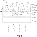
- FIG. 1 a partial view of an exemplary embodiment of a photodiode array (PDA) in accordance with the disclosure is shown in Fig. 1 and is designated generally by reference character 100.
- the systems and methods described herein can be used to facilitate assembly of PDAs with read out integrated circuits (ROICs) and to reduce pixel pitch size relative to traditional configurations.
- ROICs read out integrated circuits
- the photodiode array 100 includes an absorption layer 106, a cap layer 102 disposed on the surface 104 of the absorption layer 106, and a plurality of pixel diffusion areas 116 within the cap layer 102.
- the absorption layer 106 can be disposed on a buffer layer 108 that is on a substrate layer 110, e.g., an InP substrate, on an opposite side of the absorption layer 106 from the cap layer 102.
- a passivation layer 112 can be included on the cap layer 102 opposite from the absorption layer 106.
- Each of the pixel diffusion areas 116 extends beyond the surface 104 of the absorption layer 106 and down into the absorption layer 106 (as oriented in Fig.
- the mesa trench 124 is defined through the cap layer 102 and through the absorption layer 106.
- the sidewalls 126 of the mesa trench 124 are covered with the sidewall passivation layers 128 but with the areas of contacts 118 etched open so the metal of the contacts 118 is uncovered for electrical connection as shown in Fig. 1 .
- the sidewall passivation layers 128 combined with the space gap created by the mesa trench 124 can improve the reflection/absorbance characteristics of the absorption layer 106.
- the sidewall passivation layers 128 are shown in Fig. 1 as a single layer for sake of clarity, however the sidewall passivation layers 128 include multiple dielectric layers, which can effectively reduce dark current due to surface leakage as well as reducing stress (which would otherwise be high for thick coatings, e.g., the sidewall passivation layers 128 can be up to hundreds of nanometers thick, e.g., over 300 nm thick).
- the very top sub-layer (as oriented in Figs. 1 and 2 ) of the sidewall passivation layer 128 is a high K coating with high surface tension, which helps confine the bump metal within the contact area.
- Openings 132 through the sidewall passivation layers 128 are included to leave open each contact 118 for each pixel diffusion area 116 for electrical connection through the sidewall passivation layers 128.
- a portion 134 of the contact is sandwiched between the sidewall passivation layers 128 and the passivation layer 112.
- the final photoresist layer 130 can ultimately be removed by a liftoff process, plasma dry etch, or the like.
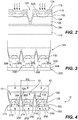
- the PDA is plasma treated, as indicated by the wavy arrows in Fig. 2 , to remove local oxidation on the contacts 118.
- the plasma treatment can utilize hydrogen, argon, and/or fluorocarbon plasma.
- Plasma treating the PDA 100 includes adjusting the surface polarity of a dielectric outer surface sub-layer of a sidewall passivation layer 128 of the PDA 100 to reduce wettability of bump material to the dielectric sub-layer.
- the outer surface sub-layer 129 of the sidewall passivation layer 128 can includes a high K material such as potassium nitride.
- the ROIC 200 is prepared with a passivation layer 202 on a substrate assembly 204.
- the interconnect bumps 206 are deposited on the ROIC 200 without a need for depositing any corresponding interconnect bumps on the PDA.
- Depositing the bumps 206 on the ROIC 200 includes depositing the bumps 206 in openings 208 in the passivation layer 202.
- the bumps 206 include indium.
- Depositing the bumps 206 on the ROIC 200 includes keeping the bumps 206 as low as 1 ⁇ m in a direction from the ROIC 200 toward the PDA 100, i.e., the bumps 206 can be less than 1 ⁇ m tall in the vertical direction as oriented in Fig.
- the bump height is adjustable, e.g., can be tailored, to fulfill the requirement of suppressing the bowing of die, a factor which is also reduced by the stress relief during the mesa isolation etch.
- the PDA 100 can be flipped, e.g., from the orientation shown in Fig. 2 to the orientation shown in Fig. 3 , and aligned with the ROIC 200 so the contacts 118 are each aligned with a respective one of the bumps 206.
- each bump 206 electrically interconnects the ROIC 200 with a respective contact 118 of the PDA 100 through metallic bonding with very low pressure required for pressing, e.g., using just the pressure from gravity.
- Assembling the PDA 100 to the ROIC 200 includes confining each bump 206 in a respective pocket 210 between the substrate assembly 204 of the ROIC 200 and the respective contact 118 of the PDA 100.
- Each respective pocket 210 is laterally bounded by the combined edges 212 and 214 of a passivation layer 202 and the sidewall passivation layer 128, respectively. While only shown in cross-section in Fig. 4 , those skilled in the art will readily appreciate that the bumps are completely enclosed because the edges 212 and 214 surround the lateral perimeter of the bumps, and the opposed substrate assembly 204 and respective contact 118 enclose the top and bottom of each pocket 210.
- assembling the PDA 100 to the ROIC 200 results in a photodetector assembly 10, wherein each bump 206 electrically connects one pixel 12 of the PDA 100 to corresponding circuit components of the ROIC 200 for forming image data based on signals generated from exposing the pixels 12.
- a pixel pitch size PS
- the pixel pitch size PS in Fig. 4 is indicated as a single length direction in cross-section, but those skilled in the art will readily appreciation that the pixels 12 can be rectangular or hexagonal, and are isolated from one another by a two-dimensional grid of the mesa trenches 124.
- Mesa structures etched into the PDA surface as disclosed herein provide relief of the stresses which traditionally lead to misalignment through wafer bowing and also provide electrical isolation between pixels.
- the etched mesas on the PDA side can mate with small e.g., ⁇ 1 um deep, ROIC bumps through intermetallic bonding.
- the traditional high-pressure pressing of excess indium materials, such as 3-5 um Indium bumps, on each side of PDA and ROIC is therefore avoided due to the much smaller ROIC bumps mating directly to the PDA contacts through intermetallic bonding. Short circuits between neighboring pixels can be completely eliminated with the disclosed interconnection structures thanks to the high pressure press-free bonding process.
- Misalignment caused by die bowing can be compensated by interconnecting the deep-trench PDA pixels (stress and bowing are released due to the deep trench etch) with the soft ROIC bumps through intermetallic bonding.
- the size of each soft ROIC bump should be sized to appropriately fill the respective pockets 210, without excessive over or under fill.
- the stress due to the coefficient of thermal expansion (CTE) mismatch between PDA and ROIC, i.e., wherein a change in temperature causes thermal expansion/compression in the PDA and ROIC at different rates, will also be reduced due to the high aspect ratio (Height: Diameter) with this interconnect structure.
- CTE coefficient of thermal expansion
Landscapes
- Solid State Image Pick-Up Elements (AREA)
- Engineering & Computer Science (AREA)
- Manufacturing & Machinery (AREA)
- Light Receiving Elements (AREA)
- Wire Bonding (AREA)
Description
- The present disclosure relates to interconnections, and more particularly to bump structures for electrically interconnecting components such as in interconnecting photodetector array components.
- Fine pitch, large format focal plane arrays (FPAs), require small interconnect bumps and minimum lateral expansion after hybridization. Traditional techniques use bumps with height to diameter ratios that make alignment difficult when interconnecting components. As a result, lateral expansion and the alignment difficulties limit how small a manufacturer can make the large format FPA pixel pitch.
- The conventional techniques have been considered satisfactory for their intended purpose. However, there is an ever present need for improved bump structures for interconnecting components like focal plane arrays. This disclosure provides a solution for this problem.
-
US 9,111,830 - A photodetector assembly includes a photodiode array (PDA). A read out integrated circuit (ROIC) is assembled to the PDA, wherein the ROIC is electrically interconnected with the PDA through a plurality of electrically conductive bumps. Each bump is confined within a respective pocket between the ROIC and a respective contact of the PDA.
- Each respective pocket is laterally bounded by edges of a passivation layer of the ROIC and a sidewall passivation layer of the PDA. The sidewall passivation layer of the PDA can include an outer surface sub-layer that includes potassium. The electrically conductive bumps can include indium. Each bump can have a dimension in a direction from the ROIC toward the PDA of as low as 1 µm or less.
- Each bump can electrically connect one pixel of the PDA to the ROIC. The PDA can have a pixel pitch size of 10 µm or less. Pixels of the PDA can be isolated from one another by mesa trenches with sidewall passivation. The mesa trenches can be etched into the PDA to provide relief of the stresses which otherwise lead to misalignment through wafer bowing and also to provide electrical isolation between pixels. Misalignment caused by die bowing can be compensated by interconnecting deep-trench PDA pixels with stress and bowing released due to the deep trench etch with soft ROIC bumps through intermetallic bonding.
- Mesas between the mesa trenches on the PDA can mate with ROIC bumps less than 1 um deep through intermetallic bonding, wherein high-pressure pressing of excess indium materials on each side of PDA and ROIC can be avoided due to the much smaller ROIC bumps mating directly to PDA contacts through intermetallic bonding, and wherein short circuits between neighboring pixels can be eliminated with this interconnection structure due to a high pressure press-free bonding process. Stress due to the coefficient of thermal expansion mismatch between the PDA and the ROIC can be reduced due to high aspect ratio (height: diameter) with this interconnect structure.
- A method of assembling a photodetector assembly includes depositing bumps on a read out integrated circuit (ROIC) without depositing bumps on a photodiode array (PDA). The method includes assembling the PDA and ROIC together wherein each bump electrically interconnects the ROIC with a respective contact of the PDA. Assembling the PDA to the ROIC includes confining each bump in a respective pocket between the ROIC and the respective contact of the PDA and laterally bounding each respective pocket by edges of: a passivation layer of the ROIC, and a sidewall passivation layer of the PDA.
- Depositing bumps on the ROIC can include using evaporation to deposit the bumps, wherein the bumps include indium.
- Depositing the bumps on the ROIC can include keeping the bumps under a dimension of 1 µm in a direction from the ROIC to the PDA.
- The bump height is adjustable to fulfill the requirement of suppressing the bowing of die, a factor which is also reduced by the stress relief during the mesa isolation etch. Assembling the PDA and ROIC together can include plasma treatment followed by reflow of the PDA and/or ROIC to achieve intermetallic bonding between the ROIC, the contacts, and the bumps, e.g., so that the traditional high press pressure for hybridization is avoided.
- The method can include plasma treating the PDA and ROIC to remove local oxidation on contacts of the PDA and ROIC. Plasma treating the PDA and ROIC can include adjusting the surface polarity of a dielectric outer surface sub-layer of a sidewall passivation layer of the PDA and ROIC to reduce wettability of bump material to the dielectric sub-layer.
- Confining each bump in the respective pocket can result in no bump material flowing out of the respective pocket.
- These and other features of the systems and methods of the subject disclosure will become more readily apparent to those skilled in the art from the following detailed description of the preferred embodiments taken in conjunction with the drawings.
- So that those skilled in the art to which the subject disclosure appertains will readily understand how to make and use the devices and methods of the subject disclosure without undue experimentation, preferred embodiments thereof will be described in detail herein below with reference to certain figures, wherein:
-
Fig. 1 is a schematic cross-sectional side elevation view of an exemplary embodiment of a photodiode array (PDA) constructed in accordance with the present disclosure, showing the sidewall passivation layer covering the sidewalls of the mesa trench with holes through the passivation for electrical connections for the contacts; -
Fig. 2 is a schematic cross-sectional side elevation view of the PDA ofFig. 1 , schematically indicating plasma treatment of the contacts; -
Fig. 3 is a schematic cross-sectional side elevation view of the PDA ofFig. 1 , showing the contacts of the PDA aligned with interconnect bumps on a read out integrated circuit (ROIC); and -
Fig. 4 is a schematic cross-sectional side elevation view of the PDA and ROIC ofFig. 3 , showing the PDA and ROIC assembled together with the interconnect bumps confined within pockets. - Reference will now be made to the drawings wherein like reference numerals identify similar structural features or aspects of the subject disclosure. For purposes of explanation and illustration, and not limitation, a partial view of an exemplary embodiment of a photodiode array (PDA) in accordance with the disclosure is shown in
Fig. 1 and is designated generally byreference character 100. Other embodiments of PDAs in accordance with the disclosure, or aspects thereof, are provided inFigs. 2-4 , as will be described. The systems and methods described herein can be used to facilitate assembly of PDAs with read out integrated circuits (ROICs) and to reduce pixel pitch size relative to traditional configurations. - The
photodiode array 100 includes anabsorption layer 106, acap layer 102 disposed on thesurface 104 of theabsorption layer 106, and a plurality ofpixel diffusion areas 116 within thecap layer 102. Theabsorption layer 106 can be disposed on abuffer layer 108 that is on asubstrate layer 110, e.g., an InP substrate, on an opposite side of theabsorption layer 106 from thecap layer 102. Apassivation layer 112 can be included on thecap layer 102 opposite from theabsorption layer 106. Each of thepixel diffusion areas 116 extends beyond thesurface 104 of theabsorption layer 106 and down into the absorption layer 106 (as oriented inFig. 1 ) to receive a charge generated from photons (indicated with the large wavy arrows inFig. 1 ) received through theabsorption layer 106 by the respectivepixel diffusion area 116. Themesa trench 124 is defined through thecap layer 102 and through theabsorption layer 106. Thesidewalls 126 of themesa trench 124 are covered with thesidewall passivation layers 128 but with the areas ofcontacts 118 etched open so the metal of thecontacts 118 is uncovered for electrical connection as shown inFig. 1 . - The
sidewall passivation layers 128 combined with the space gap created by themesa trench 124 can improve the reflection/absorbance characteristics of theabsorption layer 106. Thesidewall passivation layers 128 are shown inFig. 1 as a single layer for sake of clarity, however thesidewall passivation layers 128 include multiple dielectric layers, which can effectively reduce dark current due to surface leakage as well as reducing stress (which would otherwise be high for thick coatings, e.g., thesidewall passivation layers 128 can be up to hundreds of nanometers thick, e.g., over 300 nm thick). The very top sub-layer (as oriented inFigs. 1 and2 ) of thesidewall passivation layer 128 is a high K coating with high surface tension, which helps confine the bump metal within the contact area. -
Openings 132 through thesidewall passivation layers 128 are included to leave open eachcontact 118 for eachpixel diffusion area 116 for electrical connection through thesidewall passivation layers 128. Aportion 134 of the contact is sandwiched between thesidewall passivation layers 128 and thepassivation layer 112. - The
final photoresist layer 130 can ultimately be removed by a liftoff process, plasma dry etch, or the like. The PDA is plasma treated, as indicated by the wavy arrows inFig. 2 , to remove local oxidation on thecontacts 118. The plasma treatment can utilize hydrogen, argon, and/or fluorocarbon plasma. Plasma treating thePDA 100 includes adjusting the surface polarity of a dielectric outer surface sub-layer of asidewall passivation layer 128 of thePDA 100 to reduce wettability of bump material to the dielectric sub-layer. Theouter surface sub-layer 129 of thesidewall passivation layer 128 can includes a high K material such as potassium nitride. - With reference now to
Fig. 3 , theROIC 200 is prepared with apassivation layer 202 on asubstrate assembly 204. The interconnect bumps 206 are deposited on theROIC 200 without a need for depositing any corresponding interconnect bumps on the PDA. Depositing thebumps 206 on theROIC 200 includes depositing thebumps 206 inopenings 208 in thepassivation layer 202. Thebumps 206 include indium. Depositing thebumps 206 on theROIC 200 includes keeping thebumps 206 as low as 1 µm in a direction from theROIC 200 toward thePDA 100, i.e., thebumps 206 can be less than 1 µm tall in the vertical direction as oriented inFig. 3 , i.e., prior to assembly thePDA 100 andROIC 200 together. The bump height is adjustable, e.g., can be tailored, to fulfill the requirement of suppressing the bowing of die, a factor which is also reduced by the stress relief during the mesa isolation etch. After plasma treating thePDA 100 as discussed above with respect toFig. 2 , thePDA 100 can be flipped, e.g., from the orientation shown inFig. 2 to the orientation shown inFig. 3 , and aligned with theROIC 200 so thecontacts 118 are each aligned with a respective one of thebumps 206. - Referring now to
Fig. 4 , with thecontacts 118 aligned with thebumps 206, theROIC 200 andPDA 100 can be assembled together, e.g., by heating as indicated by the wavy arrows inFig. 4 . The heat treatment for both PDA side and ROIC side helps the intermetallic bonding formation. When assembled as shown inFig. 4 , eachbump 206 electrically interconnects theROIC 200 with arespective contact 118 of thePDA 100 through metallic bonding with very low pressure required for pressing, e.g., using just the pressure from gravity. Assembling thePDA 100 to theROIC 200 includes confining eachbump 206 in arespective pocket 210 between thesubstrate assembly 204 of theROIC 200 and therespective contact 118 of thePDA 100. Eachrespective pocket 210 is laterally bounded by the combinededges passivation layer 202 and thesidewall passivation layer 128, respectively. While only shown in cross-section inFig. 4 , those skilled in the art will readily appreciate that the bumps are completely enclosed because theedges opposed substrate assembly 204 andrespective contact 118 enclose the top and bottom of eachpocket 210. Confining eachbump 206 in therespective pocket 210 results in no bump material flowing out of therespective pocket 210, which is due not only to non-wetting surface tension characteristics in the passivation layers 202 and 128 with respect to indium, but also to the plasma treatment for top dielectric polarity charge before pressing for both the PDA and ROIC sides. Short circuits can occur in traditional PDA's when the bump material flows during assembly and contacts neighboring bumps. This can be eliminated using systems and methods as disclosed herein. Assembling thePDA 100 andROIC 200 together can include plasma treatment followed by reflow of thePDA 100 and/orROIC 200 to achieve intermetallic bonding between thecontacts 118 and thebumps 206, e.g., so that the traditional high pressure for hybridization is avoided. - With continued reference to
Fig. 4 , assembling thePDA 100 to theROIC 200 results in aphotodetector assembly 10, wherein eachbump 206 electrically connects onepixel 12 of thePDA 100 to corresponding circuit components of theROIC 200 for forming image data based on signals generated from exposing thepixels 12. Using systems and methods as disclosed herein allows for thePDA 100 to have a pixel pitch size (PS) of 10 µm or less. The pixel pitch size PS inFig. 4 is indicated as a single length direction in cross-section, but those skilled in the art will readily appreciation that thepixels 12 can be rectangular or hexagonal, and are isolated from one another by a two-dimensional grid of themesa trenches 124. - Mesa structures etched into the PDA surface as disclosed herein provide relief of the stresses which traditionally lead to misalignment through wafer bowing and also provide electrical isolation between pixels. The etched mesas on the PDA side can mate with small e.g., < 1 um deep, ROIC bumps through intermetallic bonding. The traditional high-pressure pressing of excess indium materials, such as 3-5 um Indium bumps, on each side of PDA and ROIC is therefore avoided due to the much smaller ROIC bumps mating directly to the PDA contacts through intermetallic bonding. Short circuits between neighboring pixels can be completely eliminated with the disclosed interconnection structures thanks to the high pressure press-free bonding process. Misalignment caused by die bowing can be compensated by interconnecting the deep-trench PDA pixels (stress and bowing are released due to the deep trench etch) with the soft ROIC bumps through intermetallic bonding. The size of each soft ROIC bump should be sized to appropriately fill the
respective pockets 210, without excessive over or under fill. The stress due to the coefficient of thermal expansion (CTE) mismatch between PDA and ROIC, i.e., wherein a change in temperature causes thermal expansion/compression in the PDA and ROIC at different rates, will also be reduced due to the high aspect ratio (Height: Diameter) with this interconnect structure.
Claims (14)
- A photodetector assembly comprising:a photodiode array (PDA) (100); anda read out integrated circuit (ROIC) (200) assembled to the PDA (100), wherein the ROIC (200) is electrically interconnected with the PDA (100) through a plurality of electrically conductive bumps (206), wherein each bump (206) is confined within a respective pocket (210) between the ROIC (200) and a respective contact (118) of the PDA (100); and characterised in that each respective pocket (210) is laterally bounded by edges (212, 214) of:a passivation layer (202) of the ROIC (200), anda sidewall passivation layer (128) of the PDA (100).
- The assembly as recited in claim 1, wherein the sidewall passivation layer (128) of the PDA (100) includes an outer surface sub-layer that includes potassium.
- The assembly as recited in claim 1 or 2, wherein the electrically conductive bumps (206) include indium.
- The assembly as recited in any preceding claim, wherein each bump (206) has a dimension in a direction from the ROIC (200) toward the PDA (100) of as low as 1 µm or less.
- The assembly as recited in any preceding claim, wherein the PDA (100) has a pixel pitch size of 10 µm or less, wherein each bump (206) electrically connects one pixel pitch of the PDA (100) to the ROIC (200).
- The assembly as recited in any preceding claim, wherein each bump (206) electrically connects one pixel of the PDA (100) to the ROIC (200), and wherein pixels (12) of the PDA (100) are isolated from one another by mesa trenches (124) with sidewall passivation.
- The assembly as recited claim 6, wherein the mesa trenches (124) are etched into the PDA (100) to provide relief of the stresses which otherwise lead to misalignment through wafer bowing and also to provide electrical isolation between pixels (12), and wherein misalignment caused by die bowing is compensated by interconnecting deep-trench PDA pixels with stress and bowing released due to the deep trench etch with soft ROIC bumps through intermetallic bonding.
- The assembly as recited in claim 6 or 7, wherein mesas between the mesa trenches (124) on the PDA (100) mate with ROIC bumps (206) less than 1 um deep through intermetallic bonding, wherein high-pressure pressing of excess indium materials on each side of PDA (100) and ROIC (200) is avoided due to the much smaller ROIC bumps (206) mating directly to PDA contacts (118) through intermetallic bonding, and wherein short circuits between neighboring pixels (12) are eliminated with this interconnection structure due to a high pressure press-free bonding process.
- The assembly as recited in claim 7 or 8, wherein stress due to the coefficient of thermal expansion mismatch between the PDA (100) and the ROIC (200) is reduced due to high aspect ratio (height: diameter) with this interconnect structure.
- A method of assembling a photodetector assembly comprising:depositing bumps (206) on a read out integrated circuit (ROIC) (200) without depositing bumps on a photodiode array (PDA) (100); andassembling the PDA (100) and ROIC (200) together wherein each bump (206) electrically interconnects the ROIC (200) with a respective contact (118) of the PDA (100), wherein assembling the PDA (100) to the ROIC (200) includes confining each bump (206) in a respective pocket (210) between the ROIC (200) and the respective contact (118) of the PDA (100), and wherein assembling the PDA (100) to the ROIC (200) includes laterally bounding each respective pocket (21) by edges (212, 214) of:a passivation layer (202) of the ROIC (200), anda sidewall passivation layer (128) of the PDA (100).
- The method as recited in claim 10, wherein assembling the PDA (100) and ROIC (200) together includes reflow of the PDA (100) and/or ROIC (200) to achieve intermetallic bonding between the ROIC (200), the contacts (118), and the bumps (206), so traditional high press pressure for hybridization is avoided.
- The method as recited in claim 10 or 11, further comprising:
plasma treating the PDA (100) and ROIC (200) to remove local oxidation on contacts of the PDA (100) and ROIC (200). - The method as recited in any one of claims 10-12,wherein confining each bump (206) in the respective pocket (210) results in no bump material flowing out of the respective pocket(210).
- The method as recited in any one of claims 10-13, further comprising plasma treating the PDA (100) and ROIC (200) to remove local oxidation on contacts of the PDA (100) and ROIC (200), wherein plasma treating the PDA (100) and ROIC (200) includes adjusting the surface polarity of a dielectric outer surface sub-layer of a sidewall passivation layer (128) of the PDA (100) and ROIC (200) to reduce wettability of bump material to the dielectric sub-layer.
Applications Claiming Priority (1)
| Application Number | Priority Date | Filing Date | Title |
|---|---|---|---|
| US16/129,402 US10727267B2 (en) | 2018-09-12 | 2018-09-12 | Interconnect bump structures for photo detectors |
Publications (2)
| Publication Number | Publication Date |
|---|---|
| EP3624191A1 EP3624191A1 (en) | 2020-03-18 |
| EP3624191B1 true EP3624191B1 (en) | 2021-08-04 |
Family
ID=67953684
Family Applications (1)
| Application Number | Title | Priority Date | Filing Date |
|---|---|---|---|
| EP19197065.6A Active EP3624191B1 (en) | 2018-09-12 | 2019-09-12 | Interconnect bump structures for photo detectors |
Country Status (3)
| Country | Link |
|---|---|
| US (2) | US10727267B2 (en) |
| EP (1) | EP3624191B1 (en) |
| IL (1) | IL269278B2 (en) |
Families Citing this family (6)
| Publication number | Priority date | Publication date | Assignee | Title |
|---|---|---|---|---|
| US11145786B2 (en) | 2018-09-11 | 2021-10-12 | Facebook Technologies, Llc | Methods for wafer-to-wafer bonding |
| US11342479B2 (en) | 2018-09-11 | 2022-05-24 | Facebook Technologies, Llc | Reducing bowing of materials before wafer-to-wafer bonding for LED manufacturing |
| US11056611B2 (en) * | 2018-09-11 | 2021-07-06 | Facebook Technologies, Llc | Mesa formation for wafer-to-wafer bonding |
| US11581355B2 (en) * | 2019-10-18 | 2023-02-14 | Teledyne Scientific & Imaging, Llc | Fully reticulated detectors for curved focal plane arrays |
| GB2588853B (en) * | 2019-10-18 | 2022-08-31 | Teledyne Scient & Imaging Llc | Fully reticulated detectors for curved focal plane arrays |
| US12051665B2 (en) | 2022-03-25 | 2024-07-30 | Sensors Unlimited, Inc. | Hybridization bumps for fine pitch sensor arrays |
Family Cites Families (9)
| Publication number | Priority date | Publication date | Assignee | Title |
|---|---|---|---|---|
| JPH0485961A (en) | 1990-07-30 | 1992-03-18 | Mitsubishi Electric Corp | Optical sensor |
| US6803557B1 (en) * | 2002-09-27 | 2004-10-12 | Raytheon Company | Photodiode having voltage tunable spectral response |
| US20090020700A1 (en) * | 2007-07-17 | 2009-01-22 | Locheed Martin Corporation | Method and device for generating an electrical signal in response to light |
| US7777186B2 (en) * | 2008-08-14 | 2010-08-17 | L-3 Communications Cincinnati Electronics Corporation | Pixel interconnect insulators and methods thereof |
| US8567658B2 (en) * | 2009-07-20 | 2013-10-29 | Ontos Equipment Systems, Inc. | Method of plasma preparation of metallic contacts to enhance mechanical and electrical integrity of subsequent interconnect bonds |
| US9111830B1 (en) | 2013-05-22 | 2015-08-18 | Sensors Unlimited, Inc. | Perforated blocking layer for enhanced broad band response in a focal plane array |
| US20160181325A1 (en) * | 2013-12-23 | 2016-06-23 | Paul Johnson | High pixel count short-wave to infrared image sensor |
| US10096639B2 (en) | 2016-10-10 | 2018-10-09 | Sensors Unlimited, Inc. | Bump structures for interconnecting focal plane arrays |
| US10622324B2 (en) * | 2018-02-08 | 2020-04-14 | Sensors Unlimited, Inc. | Bump structures for high density flip chip interconnection |
-
2018
- 2018-09-12 US US16/129,402 patent/US10727267B2/en active Active
-
2019
- 2019-09-11 IL IL269278A patent/IL269278B2/en unknown
- 2019-09-12 EP EP19197065.6A patent/EP3624191B1/en active Active
-
2020
- 2020-06-16 US US16/902,318 patent/US10957733B2/en active Active
Also Published As
| Publication number | Publication date |
|---|---|
| US10727267B2 (en) | 2020-07-28 |
| IL269278B1 (en) | 2023-04-01 |
| EP3624191A1 (en) | 2020-03-18 |
| US10957733B2 (en) | 2021-03-23 |
| US20200083272A1 (en) | 2020-03-12 |
| IL269278A (en) | 2020-03-31 |
| US20200312900A1 (en) | 2020-10-01 |
| IL269278B2 (en) | 2023-08-01 |
Similar Documents
| Publication | Publication Date | Title |
|---|---|---|
| US10957733B2 (en) | Interconnect bump structures for photo detectors | |
| US10879204B2 (en) | Bump structures for high density flip chip interconnection | |
| KR101087866B1 (en) | Photodiode array and its manufacturing method | |
| US9780142B1 (en) | Image sensors including conductive pixel separation structures | |
| US8174118B2 (en) | Detection device and method for manufacturing the same | |
| US6853046B2 (en) | Photodiode array and method of making the same | |
| US9559135B2 (en) | Conduction layer for stacked CIS charging prevention | |
| US11563048B2 (en) | Semiconductor device and method of manufacturing the same | |
| CN106057834A (en) | Deeply buried color filter array (cfa) by stacked grid structure | |
| US8766159B2 (en) | Multicolor detectors and applications thereof | |
| TWI790528B (en) | Image sensor and method of forming the same and semiconductor device | |
| US20070158708A1 (en) | Photodiode array, method for manufacturing same, and radiation detector | |
| US8634005B2 (en) | Very small pixel pitch focal plane array and method for manufacturing thereof | |
| KR20240121686A (en) | Frontside deep trench isolation (fdti) structure for cmos image sensor | |
| US8445983B2 (en) | Semiconductor device for performing photoelectric conversion | |
| JP5422236B2 (en) | Imaging device | |
| KR20150122866A (en) | Image sensor and method of forming the same | |
| US20250015102A1 (en) | Multiple wavelength band light sensor device | |
| JP2011100892A (en) | Electronic apparatus, composite electronic apparatus, detection device, light receiving element array, and methods of manufacturing the same | |
| EP4250360B1 (en) | Hybridization bumps for fine pitch sensor arrays | |
| US12317633B2 (en) | Radiation hardened infrared focal plane array | |
| KR101045731B1 (en) | Image sensor and manufacturing method | |
| CN121057323A (en) | An image sensor and its fabrication method | |
| CN112652636A (en) | Air gap thermal insulator for stacked chips | |
| JP2022140942A (en) | Infrared detector and manufacturing method thereof |
Legal Events
| Date | Code | Title | Description |
|---|---|---|---|
| PUAI | Public reference made under article 153(3) epc to a published international application that has entered the european phase |
Free format text: ORIGINAL CODE: 0009012 |
|
| STAA | Information on the status of an ep patent application or granted ep patent |
Free format text: STATUS: THE APPLICATION HAS BEEN PUBLISHED |
|
| AK | Designated contracting states |
Kind code of ref document: A1 Designated state(s): AL AT BE BG CH CY CZ DE DK EE ES FI FR GB GR HR HU IE IS IT LI LT LU LV MC MK MT NL NO PL PT RO RS SE SI SK SM TR |
|
| AX | Request for extension of the european patent |
Extension state: BA ME |
|
| STAA | Information on the status of an ep patent application or granted ep patent |
Free format text: STATUS: REQUEST FOR EXAMINATION WAS MADE |
|
| 17P | Request for examination filed |
Effective date: 20200914 |
|
| RBV | Designated contracting states (corrected) |
Designated state(s): AL AT BE BG CH CY CZ DE DK EE ES FI FR GB GR HR HU IE IS IT LI LT LU LV MC MK MT NL NO PL PT RO RS SE SI SK SM TR |
|
| GRAP | Despatch of communication of intention to grant a patent |
Free format text: ORIGINAL CODE: EPIDOSNIGR1 |
|
| STAA | Information on the status of an ep patent application or granted ep patent |
Free format text: STATUS: GRANT OF PATENT IS INTENDED |
|
| INTG | Intention to grant announced |
Effective date: 20210219 |
|
| GRAS | Grant fee paid |
Free format text: ORIGINAL CODE: EPIDOSNIGR3 |
|
| GRAA | (expected) grant |
Free format text: ORIGINAL CODE: 0009210 |
|
| STAA | Information on the status of an ep patent application or granted ep patent |
Free format text: STATUS: THE PATENT HAS BEEN GRANTED |
|
| AK | Designated contracting states |
Kind code of ref document: B1 Designated state(s): AL AT BE BG CH CY CZ DE DK EE ES FI FR GB GR HR HU IE IS IT LI LT LU LV MC MK MT NL NO PL PT RO RS SE SI SK SM TR |
|
| REG | Reference to a national code |
Ref country code: GB Ref legal event code: FG4D |
|
| REG | Reference to a national code |
Ref country code: AT Ref legal event code: REF Ref document number: 1417872 Country of ref document: AT Kind code of ref document: T Effective date: 20210815 |
|
| REG | Reference to a national code |
Ref country code: CH Ref legal event code: EP |
|
| REG | Reference to a national code |
Ref country code: DE Ref legal event code: R096 Ref document number: 602019006592 Country of ref document: DE |
|
| REG | Reference to a national code |
Ref country code: IE Ref legal event code: FG4D |
|
| REG | Reference to a national code |
Ref country code: LT Ref legal event code: MG9D |
|
| REG | Reference to a national code |
Ref country code: NL Ref legal event code: MP Effective date: 20210804 |
|
| REG | Reference to a national code |
Ref country code: AT Ref legal event code: MK05 Ref document number: 1417872 Country of ref document: AT Kind code of ref document: T Effective date: 20210804 |
|
| PG25 | Lapsed in a contracting state [announced via postgrant information from national office to epo] |
Ref country code: SE Free format text: LAPSE BECAUSE OF FAILURE TO SUBMIT A TRANSLATION OF THE DESCRIPTION OR TO PAY THE FEE WITHIN THE PRESCRIBED TIME-LIMIT Effective date: 20210804 Ref country code: RS Free format text: LAPSE BECAUSE OF FAILURE TO SUBMIT A TRANSLATION OF THE DESCRIPTION OR TO PAY THE FEE WITHIN THE PRESCRIBED TIME-LIMIT Effective date: 20210804 Ref country code: ES Free format text: LAPSE BECAUSE OF FAILURE TO SUBMIT A TRANSLATION OF THE DESCRIPTION OR TO PAY THE FEE WITHIN THE PRESCRIBED TIME-LIMIT Effective date: 20210804 Ref country code: FI Free format text: LAPSE BECAUSE OF FAILURE TO SUBMIT A TRANSLATION OF THE DESCRIPTION OR TO PAY THE FEE WITHIN THE PRESCRIBED TIME-LIMIT Effective date: 20210804 Ref country code: BG Free format text: LAPSE BECAUSE OF FAILURE TO SUBMIT A TRANSLATION OF THE DESCRIPTION OR TO PAY THE FEE WITHIN THE PRESCRIBED TIME-LIMIT Effective date: 20211104 Ref country code: AT Free format text: LAPSE BECAUSE OF FAILURE TO SUBMIT A TRANSLATION OF THE DESCRIPTION OR TO PAY THE FEE WITHIN THE PRESCRIBED TIME-LIMIT Effective date: 20210804 Ref country code: LT Free format text: LAPSE BECAUSE OF FAILURE TO SUBMIT A TRANSLATION OF THE DESCRIPTION OR TO PAY THE FEE WITHIN THE PRESCRIBED TIME-LIMIT Effective date: 20210804 Ref country code: NO Free format text: LAPSE BECAUSE OF FAILURE TO SUBMIT A TRANSLATION OF THE DESCRIPTION OR TO PAY THE FEE WITHIN THE PRESCRIBED TIME-LIMIT Effective date: 20211104 Ref country code: PT Free format text: LAPSE BECAUSE OF FAILURE TO SUBMIT A TRANSLATION OF THE DESCRIPTION OR TO PAY THE FEE WITHIN THE PRESCRIBED TIME-LIMIT Effective date: 20211206 Ref country code: HR Free format text: LAPSE BECAUSE OF FAILURE TO SUBMIT A TRANSLATION OF THE DESCRIPTION OR TO PAY THE FEE WITHIN THE PRESCRIBED TIME-LIMIT Effective date: 20210804 |
|
| PG25 | Lapsed in a contracting state [announced via postgrant information from national office to epo] |
Ref country code: PL Free format text: LAPSE BECAUSE OF FAILURE TO SUBMIT A TRANSLATION OF THE DESCRIPTION OR TO PAY THE FEE WITHIN THE PRESCRIBED TIME-LIMIT Effective date: 20210804 Ref country code: LV Free format text: LAPSE BECAUSE OF FAILURE TO SUBMIT A TRANSLATION OF THE DESCRIPTION OR TO PAY THE FEE WITHIN THE PRESCRIBED TIME-LIMIT Effective date: 20210804 Ref country code: GR Free format text: LAPSE BECAUSE OF FAILURE TO SUBMIT A TRANSLATION OF THE DESCRIPTION OR TO PAY THE FEE WITHIN THE PRESCRIBED TIME-LIMIT Effective date: 20211105 |
|
| PG25 | Lapsed in a contracting state [announced via postgrant information from national office to epo] |
Ref country code: NL Free format text: LAPSE BECAUSE OF FAILURE TO SUBMIT A TRANSLATION OF THE DESCRIPTION OR TO PAY THE FEE WITHIN THE PRESCRIBED TIME-LIMIT Effective date: 20210804 |
|
| PG25 | Lapsed in a contracting state [announced via postgrant information from national office to epo] |
Ref country code: DK Free format text: LAPSE BECAUSE OF FAILURE TO SUBMIT A TRANSLATION OF THE DESCRIPTION OR TO PAY THE FEE WITHIN THE PRESCRIBED TIME-LIMIT Effective date: 20210804 |
|
| REG | Reference to a national code |
Ref country code: DE Ref legal event code: R097 Ref document number: 602019006592 Country of ref document: DE |
|
| REG | Reference to a national code |
Ref country code: BE Ref legal event code: MM Effective date: 20210930 |
|
| PG25 | Lapsed in a contracting state [announced via postgrant information from national office to epo] |
Ref country code: SM Free format text: LAPSE BECAUSE OF FAILURE TO SUBMIT A TRANSLATION OF THE DESCRIPTION OR TO PAY THE FEE WITHIN THE PRESCRIBED TIME-LIMIT Effective date: 20210804 Ref country code: SK Free format text: LAPSE BECAUSE OF FAILURE TO SUBMIT A TRANSLATION OF THE DESCRIPTION OR TO PAY THE FEE WITHIN THE PRESCRIBED TIME-LIMIT Effective date: 20210804 Ref country code: RO Free format text: LAPSE BECAUSE OF FAILURE TO SUBMIT A TRANSLATION OF THE DESCRIPTION OR TO PAY THE FEE WITHIN THE PRESCRIBED TIME-LIMIT Effective date: 20210804 Ref country code: MC Free format text: LAPSE BECAUSE OF FAILURE TO SUBMIT A TRANSLATION OF THE DESCRIPTION OR TO PAY THE FEE WITHIN THE PRESCRIBED TIME-LIMIT Effective date: 20210804 Ref country code: EE Free format text: LAPSE BECAUSE OF FAILURE TO SUBMIT A TRANSLATION OF THE DESCRIPTION OR TO PAY THE FEE WITHIN THE PRESCRIBED TIME-LIMIT Effective date: 20210804 Ref country code: CZ Free format text: LAPSE BECAUSE OF FAILURE TO SUBMIT A TRANSLATION OF THE DESCRIPTION OR TO PAY THE FEE WITHIN THE PRESCRIBED TIME-LIMIT Effective date: 20210804 Ref country code: AL Free format text: LAPSE BECAUSE OF FAILURE TO SUBMIT A TRANSLATION OF THE DESCRIPTION OR TO PAY THE FEE WITHIN THE PRESCRIBED TIME-LIMIT Effective date: 20210804 |
|
| PLBE | No opposition filed within time limit |
Free format text: ORIGINAL CODE: 0009261 |
|
| STAA | Information on the status of an ep patent application or granted ep patent |
Free format text: STATUS: NO OPPOSITION FILED WITHIN TIME LIMIT |
|
| 26N | No opposition filed |
Effective date: 20220506 |
|
| PG25 | Lapsed in a contracting state [announced via postgrant information from national office to epo] |
Ref country code: LU Free format text: LAPSE BECAUSE OF NON-PAYMENT OF DUE FEES Effective date: 20210912 Ref country code: IT Free format text: LAPSE BECAUSE OF FAILURE TO SUBMIT A TRANSLATION OF THE DESCRIPTION OR TO PAY THE FEE WITHIN THE PRESCRIBED TIME-LIMIT Effective date: 20210804 Ref country code: IE Free format text: LAPSE BECAUSE OF NON-PAYMENT OF DUE FEES Effective date: 20210912 Ref country code: BE Free format text: LAPSE BECAUSE OF NON-PAYMENT OF DUE FEES Effective date: 20210930 |
|
| PG25 | Lapsed in a contracting state [announced via postgrant information from national office to epo] |
Ref country code: SI Free format text: LAPSE BECAUSE OF FAILURE TO SUBMIT A TRANSLATION OF THE DESCRIPTION OR TO PAY THE FEE WITHIN THE PRESCRIBED TIME-LIMIT Effective date: 20210804 |
|
| REG | Reference to a national code |
Ref country code: CH Ref legal event code: PL |
|
| PG25 | Lapsed in a contracting state [announced via postgrant information from national office to epo] |
Ref country code: CY Free format text: LAPSE BECAUSE OF FAILURE TO SUBMIT A TRANSLATION OF THE DESCRIPTION OR TO PAY THE FEE WITHIN THE PRESCRIBED TIME-LIMIT Effective date: 20210804 |
|
| PG25 | Lapsed in a contracting state [announced via postgrant information from national office to epo] |
Ref country code: LI Free format text: LAPSE BECAUSE OF NON-PAYMENT OF DUE FEES Effective date: 20220930 Ref country code: HU Free format text: LAPSE BECAUSE OF FAILURE TO SUBMIT A TRANSLATION OF THE DESCRIPTION OR TO PAY THE FEE WITHIN THE PRESCRIBED TIME-LIMIT; INVALID AB INITIO Effective date: 20190912 Ref country code: CH Free format text: LAPSE BECAUSE OF NON-PAYMENT OF DUE FEES Effective date: 20220930 |
|
| PG25 | Lapsed in a contracting state [announced via postgrant information from national office to epo] |
Ref country code: MK Free format text: LAPSE BECAUSE OF FAILURE TO SUBMIT A TRANSLATION OF THE DESCRIPTION OR TO PAY THE FEE WITHIN THE PRESCRIBED TIME-LIMIT Effective date: 20210804 |
|
| PG25 | Lapsed in a contracting state [announced via postgrant information from national office to epo] |
Ref country code: TR Free format text: LAPSE BECAUSE OF FAILURE TO SUBMIT A TRANSLATION OF THE DESCRIPTION OR TO PAY THE FEE WITHIN THE PRESCRIBED TIME-LIMIT Effective date: 20210804 |
|
| PG25 | Lapsed in a contracting state [announced via postgrant information from national office to epo] |
Ref country code: MT Free format text: LAPSE BECAUSE OF FAILURE TO SUBMIT A TRANSLATION OF THE DESCRIPTION OR TO PAY THE FEE WITHIN THE PRESCRIBED TIME-LIMIT Effective date: 20210804 |
|
| REG | Reference to a national code |
Ref country code: DE Ref legal event code: R079 Ref document number: 602019006592 Country of ref document: DE Free format text: PREVIOUS MAIN CLASS: H01L0027146000 Ipc: H10F0039180000 |
|
| PGFP | Annual fee paid to national office [announced via postgrant information from national office to epo] |
Ref country code: DE Payment date: 20250820 Year of fee payment: 7 |
|
| PGFP | Annual fee paid to national office [announced via postgrant information from national office to epo] |
Ref country code: GB Payment date: 20250822 Year of fee payment: 7 |
|
| PGFP | Annual fee paid to national office [announced via postgrant information from national office to epo] |
Ref country code: FR Payment date: 20250820 Year of fee payment: 7 |
|
| P01 | Opt-out of the competence of the unified patent court (upc) registered |
Free format text: CASE NUMBER: UPC_APP_0018995_3624191/2025 Effective date: 20251222 |