EP3623824A1 - Load state detection circuit and method - Google Patents
Load state detection circuit and method Download PDFInfo
- Publication number
- EP3623824A1 EP3623824A1 EP19188497.2A EP19188497A EP3623824A1 EP 3623824 A1 EP3623824 A1 EP 3623824A1 EP 19188497 A EP19188497 A EP 19188497A EP 3623824 A1 EP3623824 A1 EP 3623824A1
- Authority
- EP
- European Patent Office
- Prior art keywords
- load
- tested
- voltage
- terminal
- power supply
- Prior art date
- Legal status (The legal status is an assumption and is not a legal conclusion. Google has not performed a legal analysis and makes no representation as to the accuracy of the status listed.)
- Granted
Links
Images




Classifications
-
- G—PHYSICS
- G01—MEASURING; TESTING
- G01R—MEASURING ELECTRIC VARIABLES; MEASURING MAGNETIC VARIABLES
- G01R31/00—Arrangements for testing electric properties; Arrangements for locating electric faults; Arrangements for electrical testing characterised by what is being tested not provided for elsewhere
- G01R31/50—Testing of electric apparatus, lines, cables or components for short-circuits, continuity, leakage current or incorrect line connections
- G01R31/52—Testing for short-circuits, leakage current or ground faults
-
- G—PHYSICS
- G01—MEASURING; TESTING
- G01R—MEASURING ELECTRIC VARIABLES; MEASURING MAGNETIC VARIABLES
- G01R31/00—Arrangements for testing electric properties; Arrangements for locating electric faults; Arrangements for electrical testing characterised by what is being tested not provided for elsewhere
- G01R31/005—Testing of electric installations on transport means
- G01R31/006—Testing of electric installations on transport means on road vehicles, e.g. automobiles or trucks
- G01R31/007—Testing of electric installations on transport means on road vehicles, e.g. automobiles or trucks using microprocessors or computers
-
- G—PHYSICS
- G01—MEASURING; TESTING
- G01R—MEASURING ELECTRIC VARIABLES; MEASURING MAGNETIC VARIABLES
- G01R31/00—Arrangements for testing electric properties; Arrangements for locating electric faults; Arrangements for electrical testing characterised by what is being tested not provided for elsewhere
- G01R31/327—Testing of circuit interrupters, switches or circuit-breakers
-
- G—PHYSICS
- G01—MEASURING; TESTING
- G01R—MEASURING ELECTRIC VARIABLES; MEASURING MAGNETIC VARIABLES
- G01R31/00—Arrangements for testing electric properties; Arrangements for locating electric faults; Arrangements for electrical testing characterised by what is being tested not provided for elsewhere
- G01R31/50—Testing of electric apparatus, lines, cables or components for short-circuits, continuity, leakage current or incorrect line connections
- G01R31/54—Testing for continuity
-
- H—ELECTRICITY
- H02—GENERATION; CONVERSION OR DISTRIBUTION OF ELECTRIC POWER
- H02H—EMERGENCY PROTECTIVE CIRCUIT ARRANGEMENTS
- H02H1/00—Details of emergency protective circuit arrangements
- H02H1/0007—Details of emergency protective circuit arrangements concerning the detecting means
-
- H—ELECTRICITY
- H02—GENERATION; CONVERSION OR DISTRIBUTION OF ELECTRIC POWER
- H02H—EMERGENCY PROTECTIVE CIRCUIT ARRANGEMENTS
- H02H3/00—Emergency protective circuit arrangements for automatic disconnection directly responsive to an undesired change from normal electric working condition with or without subsequent reconnection ; integrated protection
- H02H3/16—Emergency protective circuit arrangements for automatic disconnection directly responsive to an undesired change from normal electric working condition with or without subsequent reconnection ; integrated protection responsive to fault current to earth, frame or mass
Definitions
- the present disclosure relates to the field of circuit technology, especially a load state detection circuit and a load state detection method.
- Some embodiments of the present disclosure provides a load state detection circuit including at least a detecting power supply, a voltage sampling circuit, a switch unit, and a microcontroller.
- the microcontroller is connected to the switch unit which is connected between the detecting power supply and the load to be tested.
- a voltage sampling point is formed at either terminal of the load to be tested, and the voltage sampling circuit is connected between the voltage sampling point and the microcontroller.
- the voltage sampling circuit is configured to sample a voltage at the voltage sampling point, and output the voltage to the microcontroller.
- the microcontroller is configured to connect the load to be tested and the detecting power supply by controlling the switch unit, and determine whether a fault exists in the load to be tested according to a received voltage at the voltage sampling point sampled by the voltage sampling circuit, before conductively connecting the load to be tested with the drive power supply.
- the microcontroller is further configured to disconnect the load to be tested from the detecting power supply and control conduction between the load to be tested and the drive power supply by controlling the switch unit when it is determined that no fault exists in the load to be tested.
- Some embodiments of the present disclosure further provides a load state detection method applied to a microcontroller of a load state detection circuit including at least a detecting power supply, a voltage sampling circuit, a switch unit, and a microcontroller.
- the load to be tested Before conductively connecting the load to be tested with the drive power supply, the load to be tested is connected with the detecting power supply by controlling the switch unit, a voltage sampled by the voltage sampling circuit at the voltage sampling point is received, and it is determined whether a fault exists in the load to be tested according to a voltage sampled by the voltage sampling circuit at the voltage sampling point.
- the switch unit is controlled to disconnect the load to be tested from the detecting power supply and control conduction between the load to be tested and the drive power supply, when it is determined that no fault exists in the load to be tested.
- the load to be tested and the detecting power supply are connected by controlling the switch unit.
- a voltage at the voltage sampling point (the voltage sampling point is formed at either terminal of the load to be tested) is sampled by the voltage sampling circuit, it is determined whether a fault exists in the load to be tested according to the received voltage at the voltage sampling point, and when it is determined that no fault exists in the load to be tested, the load to be tested is disconnected from the detecting power supply by controlling the switch unit, so as to avoid interference of the detecting power supply, and power on the load to be tested.
- the load to be tested before the load to be tested is powered on, it is possible to determine in advance whether a fault exists in the load to be tested.
- the load to be tested will not be powered on until it is determined that no fault exists in the load to be tested, thereby safety is improved.
- the microcontroller is configured to disconnect the load to be tested from the detecting power supply by controlling the switch unit, and determine whether the load to be tested and the drive power supply are short-circuited according to whether the received voltage at the voltage sampling point is a voltage of the drive power supply, before conductively connecting the load to be tested with the drive power supply.
- This embodiment provides a specific implementation of how to determine whether a load to be tested and a drive power supply are short-circuited.
- the load state detection circuit further includes a first voltage divider circuit.
- the switch unit is connected to a first terminal of the first voltage divider circuit, a second terminal of the first voltage divider circuit is connected to an terminal of the load to be tested, and a third terminal of the first voltage divider circuit is grounded.
- the first voltage divider circuit arranged at the voltage sampling point prevents the voltage sampled by the voltage sampling circuit from being too high to damage the microcontroller.
- the first voltage divider circuit includes a first resistor network and a second resistor network.
- the switch unit is connected to one terminal of the first resistor network, the other terminal of the first resistor network is connected to an terminal of the second resistor network, and the other terminal of the second resistor network is grounded.
- the one terminal of the first resistor network forms the first terminal of the first voltage divider circuit.
- a junction of the first resistor network and second resistor network is connected to a terminal of the load to be tested where the voltage sampling point is formed.
- the junction of the first resistor network and second resistor network forms the second terminal of the first voltage divider circuit.
- the switch unit is a first switch whose control terminal is connected to the microcontroller, one terminal of the first switch is connected to at least one detecting power supply, the other terminal of the first switch is connected to the first terminal of the first voltage divider circuit, and the second terminal of the first voltage divider circuit is connected to an terminal of the load to be tested where the voltage sampling point is formed.
- the microcontroller is specifically configured to control the first switch to switch on, determine that a grounding short circuit fault occurs to an terminal of the load to be tested where the voltage sampling point is formed when the received voltage at the voltage sampling point is equal to zero, and determine that a grounding short circuit fault occurs to an terminal of the load to be tested where no voltage sampling point is formed when the received voltage at the voltage sampling point is within a first preset range.
- This embodiment provides an implementation of determining a specific fault type of the load to be tested when the switch unit is the first switch and the second terminal of the first voltage divider circuit is connected to a terminal of the load to be tested where a voltage sampling point is formed.
- the switch unit is the first switch whose control terminal is connected to the microcontroller, one terminal of the first switch is connected to at least one detecting power supply, the other terminal of the first switch is connected to the first terminal of the first voltage divider circuit, and the second terminal of the first voltage divider circuit is connected to an terminal of the load to be tested where no voltage sampling point is formed.
- the microcontroller is specifically configured to control the first switch to switch on, and determine that a fault occurs to the load to be tested when the received voltage at the voltage sampling point is equal to zero. This embodiment provides an implementation of determining whether a fault exists in the load to be tested when the switch unit is the first switch and the second terminal of the first voltage divider circuit is connected to an terminal of the load to be tested where no voltage sampling point is formed.
- the switch unit includes a second switch and a third switch.
- a control terminal of the second switch and a control terminal of the third switch are respectively connected to the microcontroller
- the load state detection circuit further includes a second voltage divider circuit.
- a first terminal of the second switch and a first terminal of the third switch are respectively connected to the at least one detecting power supply, a second terminal of the second switch is connected to the first terminal of the first voltage divider circuit, a second terminal of the third switch is connected to a first terminal of the second voltage divider circuit, the second terminal of the first voltage divider circuit and a second terminal of the second voltage divider circuit are connected to two terminals of the load to be tested, respectively, and a third terminal of the second voltage divider circuit is grounded.
- the microcontroller is specifically configured to control the second switch to switch on, determine that a grounding short circuit fault occurs to an terminal of the load to be tested where the voltage sampling point is formed when the received voltage at the voltage sampling point is equal to zero, and determine that a grounding short circuit fault occurs to an terminal of the load to be tested where no voltage sampling point is formed when the received voltage at the voltage sampling point is within the first preset range.
- This embodiment provides an implementation of determining a specific fault type of the load to be tested when the switch unit includes the second switch and third switch.
- the microcontroller is configured to control the second switch to switch off and the third switch to switch on, and determine that an open circuit fault occurs to the load to be tested when the received voltage at the voltage sampling point is equal to zero. This embodiment provides a specific implementation of determining whether an open-circuit fault occurs to the load to be tested.
- the voltage sampling circuit includes a filter unit and an analog-to-digital converter.
- a first terminal of the analog-to-digital converter is connected to the voltage sampling point via the filter unit, while a second terminal of the analog-to-digital converter is connected to the microcontroller.
- This embodiment provides a specific structure of a voltage sampling circuit.
- the load state detection circuit includes at least one anti-reverse diode, and at least one terminal of the load to be tested is connected to the switch unit via the at least one anti-reverse diode.
- an anti-reverse diode is arranged between the detecting power supply and the load to be tested to avoid countercurrent, which protects the detection circuit, and prevents a detecting loop from being interfered, which may have affected judgment on a fault of the load to be tested.
- a resistance value of the first resistor network and second resistor network is greater than an internal resistance of the load to be tested. This embodiment may prevent the detecting power supply from powering on the load to be tested during detection, which may achieve testing the load to be tested in a case where the detecting power supply has not power on the load to be tested.
- some embodiments of the present disclosure relates to a load state detection circuit for detecting whether a fault exists in a load to be tested.
- the load to be tested may be a load in an electric vehicle, such as a relay, a water pump, a valve and so on, and the load to be tested is powered on by a drive power supply.
- the drive power supply may be a drive power supply of the electric vehicle.
- the present disclosure is not limited hereto, but it may otherwise be another power supply in the electric vehicle.
- the load state detection circuit includes at least one detecting power supply 1, a voltage sampling circuit 2, a switch unit 3 and a microcontroller 4.
- the microcontroller 4 is connected to the switch unit 3 which is connected between the detecting power supply and a terminal of a load 5 to be tested. That is, one terminal of the switch unit 3 is connected to the detecting power supply 1, while the other terminal of the switch unit 3 is connected to a terminal of the load to be tested.
- a voltage sampling point T is formed at either terminal of the load 5 to be tested.
- the voltage sampling circuit 2 is connected between the voltage sampling point T and the microcontroller 4.
- the voltage sampling circuit 2 is configured to sample a voltage at the voltage sampling point T, and output the voltage to the microcontroller 4.
- the voltage sampling circuit 2 includes a filter unit 21 and an analog-to-digital converter 22, wherein a first terminal of the analog-to-digital converter 22 is connected to the voltage sampling point T via the filter unit 21, while a second terminal of the analog-to-digital converter 22 is connected to the microcontroller 4.
- An interference signal in the voltage at the voltage sampling point T is filtered by the filter unit 21 to improve accuracy of the voltage sampled by the analog-to-digital converter 22.
- the filter unit 21 may be a capacitor. During detection, it may select an appropriate delay time according to charge and discharge time of the capacitor for detection.
- an analog-to-digital converter ADC inside the microcontroller 4 may be used as the analog-to-digital converter 22 of the voltage sampling circuit 2.
- the present disclosure is not limited hereto, but other sampling chip may otherwise be used as the voltage sampling circuit 2.
- the microcontroller 4 is configured to connect the load 5 to be tested and the detecting power supply 1 by controlling the switch unit 3, and determine whether a fault exists in the load 5 to be tested according to a received voltage at the voltage sampling point T sampled by the voltage sampling circuit 2, before conductively connecting the load 5 to be tested and the drive power supply 6.
- the conduction of the drive power supply 6 with the load 5 to be tested is simultaneously controlled by a high-side drive unit 7 and a low-side drive unit 8.
- the drive power supply 6 is connected to a high-side of the load 5 to be tested via the high-side drive unit 7.
- a low-side of the load 5 to be tested is grounded via the low-side drive unit 8.
- the load 5 to be tested is conductively connected with the drive power supply 6, means that, the drive power supply powers the load 5 to be tested on.
- the "power on (or conductively connect)" herein refers to that the drive power supply provides enough large current and drive the load 5 to be tested to work. That the load 5 to be tested is connected with the detecting power supply 1 means the load 5 to be tested is electrically connected with the detecting power supply 1 but the detecting power supply 1 does not power on the load 5 to be tested; herein, the detecting power supply 1 is electrically connected with the load 5 to be tested, but provides small current not enough for driving the load 5 to be tested to work.
- the load state detection circuit further includes at least an anti-reverse diode D1. At least one terminal is connected to the switch unit via at least the anti-reverse diode D1 to avoid countercurrent and protect the detection circuit. Besides, a detecting loop is prevented from being interfered, thereby judgment on a fault of the load 5 to be tested is not affected.
- the microcontroller 4 is further configured to control conduction between the load 5 to be tested and the drive power supply 6, and disconnect the load 5 to be tested from the detecting power supply by controlling the switch unit 3, when it is determined that no fault exists in the load 5 to be tested.
- connection relationships between the microcontroller 4 and the three of the switch unit 3, the high-side drive unit 7 and the low-side drive unit 8 are not embodied in the drawings to maintain clearness of the figures.
- the switch unit 3, the high-side drive unit 7, and the low-side drive unit 8 are all controlled by the microcontroller 4.
- FIGs. 2 and 3 will be taken as examples for a detailed description of a way in which a load state detection circuit determines a fault of a load 5 to be tested.
- a drive power supply 6 is connected to the high-side of the load 5 to be tested via a high-side drive unit 7, and a low-side of the load 5 to be tested is grounded via a low-side drive unit 8.
- the microcontroller 4 outputs a control signal to control the high-side drive unit 7 and the low-side drive unit 8.
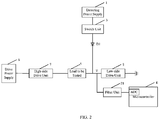
- the detecting power supply 1 is connected to the switch unit 3, and the switch unit 3 is connected to the low-side of the load 5 to be tested via the anti-reverse diode D1.
- the voltage sampling point T is formed at the low-side of the load 5 to be tested.
- a first terminal of the filter unit 21 is connected to the voltage sampling point T, and a second terminal of the filter unit 21 is connected to an ADC in the microcontroller 4.
- the voltage sampling point T is formed at the low-side of the load 5 to be tested is taken as an example for description, to which the present disclosure is not limited, but the voltage sampling point T may otherwise be formed at the high-side of the load 5 to be tested.
- the high-side of the load 5 to be tested refers to the terminal connected to the positive electrode of the drive power supply 6, and the low-side of the load 5 to be tested refers to the terminal connected to the negative electrode of the drive power supply 6.
- grounding in the context means being connected to the detecting power supply 1 and the negative electrode of the drive power supply 6.
- the microcontroller 4 connects the detecting power supply 1 and the low-side of the load 5 to be tested by controlling the switch unit 3.
- the ADC in the microcontroller 4 samples a voltage V T at the voltage sampling point T.
- the microcontroller 4 determines that a grounding short circuit fault occurs to the low-side of the load 5 to be tested when V T is equal to zero. It shall be noted that, in practice, due to an ADC sampling error, a transmission line impedance, a software calculation error and so on, a fluctuation value V b may be preset, and when V T ⁇ V b , it may be determined that a grounding short circuit occurs to the low-side of the load 5 to be tested.
- the drive power supply 6 is connected to the high-side of the load 5 to be tested via the high-side drive unit 7, and the low-side of the load 5 to be tested is grounded via the low-side drive unit 8.
- the microcontroller 4 outputs a control signal to control the high side drive unit 7 and the low side drive unit 8.
- the detecting power supply 1 is connected to the anti-reverse diode D1 which is connected to the high-side of the load 5 to be tested via the switch unit 3.
- a voltage sampling point T is formed at the low-side of the load 5 to be tested.
- the first terminal of the filter unit 21 is connected to the voltage sampling point T, and the second terminal of the filter unit 21 is connected to the ADC in the microcontroller 4.
- the microcontroller 4 connects the detecting power supply 1 with the high-side of the load 5 to be tested by controlling the switch unit 3.
- the ADC in the microcontroller 4 samples the voltage V T at the voltage sampling point T.
- the microcontroller 4 determines that a fault occurs to the load 5 to be tested when V T is equal to a theoretical value zero or fluctuates within a certain range of the theoretical value zero.
- the microcontroller 4 is further configured to disconnect the load 5 to be tested from the detecting power supply 1 by controlling the switch unit 3, and determine whether the load 5 to be tested and the drive power supply 6 are short-circuited according to whether the received voltage at the voltage sampling point T is a voltage of the drive power supply 6, before conductively connecting the load 5 to be tested with the drive power supply 6. Take FIG. 2 as an example.
- the microcontroller 4 disconnects the detecting power supply 1 from the low-side of the load 5 to be tested by controlling the switch unit 3, and the ADC in the microcontroller 4 samples the voltage V T at the voltage sampling point T.
- the microcontroller 4 determines that the load 5 to be tested and the drive power supply 6 are short-circuited when V T is equal to the voltage of the drive power supply 6 or fluctuates within a certain range of the voltage of the drive power supply 6.
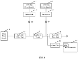
- FIGs. 2 and 3 may be combined to form a load state detection circuit as shown in FIG. 4 where there are two detecting power supplies 1 and two switch units 3.
- the two detecting power supplies 1 are connected to the anti-reverse diode D1 and the anti-reverse diode D2 via two switch unit 3, respectively.
- the anti-reverse diode D1 and the anti-reverse diode D2 are connected to two terminals of the load 5 to be tested, respectively.
- the voltage sampling point T may be formed at the high-side or low-side of the load 5 to be tested (the figure takes forming a low terminal of the load 5 as an example), so as to implement all detection functions of FIGs. 2 and 3 as described above.
- the two detecting power supplies 1 may be identical or different, to which this disclosure does not impose any limitation.
- the anti-reverse diode may not be provided, to which this disclosure does not impose any limitation.
- the load to be tested and the detecting power supply are connected by controlling the switch unit.
- a voltage at the voltage sampling point (the voltage sampling point is formed at either terminal of the load to be tested) is sampled by the voltage sampling circuit, it is determined whether a fault exists in the load to be tested according to the received voltage at the voltage sampling point, and when it is determined that no fault exists in the load to be tested, the load to be tested is disconnected from the detecting power supply by controlling the switch unit so as to avoid interference of the detecting power supply, and power on the load to be tested.
- the load to be tested before the load to be tested is powered on, it is possible to determine in advance whether a fault exists in the load to be tested.
- the load to be tested will not be powered on until it is determined that no fault exists in the load to be tested, thereby safety is improved.
- the load state detection circuit further includes a first voltage divider circuit 10.
- the switch unit 3 is connected to a first terminal of the first voltage divider circuit 10.
- a second terminal of the first voltage divider circuit 10 is connected to the load 5 to be tested.
- a third terminal of the first voltage divider circuit 10 is grounded.
- the first voltage divider circuit 10 includes a first resistor network and a second resistor network.
- the switch unit 3 is connected to one terminal of the first resistor network, and the other terminal of the first resistor network is connected to a terminal of the second resistor network.
- the one terminal of the first resistor network forms the first terminal of the first voltage divider circuit 10.
- a junction K of the first resistor network and second resistor network forms the second terminal of the first voltage divider circuit 10
- the other terminal of the second resistor network forms the third terminal of the first voltage divider circuit 10.
- first resistor network is a first resistor R1 and the second resistor network is a second resistor R2 is taken as an example for description, but this disclosure does not impose any limitation to the specific structures of the first resistor network and the second resistor network.
- the detecting power supply 1 is connected to the first terminal of the first voltage divider circuit 10 via the switch unit 3, and the second terminal of the first voltage divider circuit 10 is connected to the low-side of the load 5 to be tested, and the voltage sampling point T is formed at the low-side of the load 5 to be tested.
- a resistance value of the first resistor network and a resistance value of the second resistor network are greater than an internal resistance r of the load 5 to be tested.
- the resistance value of the first resistor R1 and the resistance value of the second resistor R2 are ten times the internal resistance r of the load 5 to be tested, thereby reducing current in the circuit when performing detection. While, generally, large current is needed when powering on the load 5 to be tested. That is, the load 5 to be tested is detected in a case when the detecting power supply 1 does not power on the load 5 to be tested.
- the first voltage divider circuit arranged at the voltage sampling point prevents the voltage sampled by the voltage sampling circuit from being too high to damage the microcontroller. Besides, a specific structure of the first voltage divider circuit is provided.
- FIG. 6 it is provided a specific way of determining a fault in the load to be tested when the switch unit 3 is a first switch K1.
- the switch unit 3 is the first switch K1 whose control terminal is connected to the microcontroller 4.
- the microcontroller 4 may control switch on and switch off of the first switch K1.
- One terminal of the first switch K1 is connected to the detecting power supply 1, and the other terminal of the first switch K1 is connected to the first terminal of the first voltage divider circuit 10.
- the microcontroller 4 is specifically configured to control the first switch K1 to switch on and receive the sampled voltage V T by the ADC at the voltage sampling point T.
- V T is equal to zero
- the microcontroller 4 determines that a grounding short circuit fault occurs to the terminal of the load 5 to be tested where the voltage sampling point T is formed, that is, a grounding short circuit occurs to the low-side of the load 5 to be tested as shown in FIG. 6 .
- the microcontroller 4 determines that a grounding short circuit fault occurs to the terminal of the load 5 to be tested where the voltage sampling point T is not formed, that is, the grounding short circuit fault occurs to the high-side of the load 5 to be tested as shown in FIG. 6 .
- the first preset range shall be set according to the first resistor R1, the second resistor R2, the internal resistance r of the load 5 to be tested, and the voltage V of the detecting power supply. Specifically, suppose a grounding short circuit fault occurs to the high-side of the load 5 to be tested, then a theoretical value of the voltage V T at the voltage sampling point T is V*r*R2/(r *R2+R1* r +R1*R2).
- V b1 a fluctuation value V b1 is preset on the basis of the theoretical value, it may be obtained that the first preset range is [V*r*R2/(r *R2+R1* r +R1*R2)-V b1 , V*r*R2/(r *R2+R1* r +R1*R2)+ V b1 ],
- the microcontroller 4 is specifically configured to control the first switch K1 to switch on.
- the received voltage V T at the voltage sampling point T is equal to the theoretical value zero, or fluctuates within a certain range of the theoretical value zero, it is determined that a fault occurs to the load 5 to be tested.
- the microcontroller 4 determines whether the load 5 to be tested and the drive power supply 6 are short-circuited by controlling the first switch K1 to disconnect the load 5 to be tested from the detecting power supply 1 and according to whether the received voltage at the voltage sampling point T is a voltage of the drive power supply 6. Take FIG. 6 for example, where the microcontroller 4 controls the first switch K1 to disconnect the detecting power supply 1 from the low-side of the load 5 to be tested.
- V Q represents a voltage of the drive power supply 6
- r represents an internal resistance of the load 5 to be tested.
- the load state detection circuit of the disclosure may further test a plurality of loads 5 to be tested at the same time.
- FIG. 8 that there are two loads 5 to be tested is taken as an example.
- the way to determine a fault of the each of the loads 5 to be tested is similar to the above described, and will not be repeated here. Therefore, the microcontroller 4 may determine whether to power on the loads 5 to be tested according to types of the loads and fault statuses of the loads, which is more secure.
- the switch unit 3 includes a second switch K2 and a third switch K3.
- the switch unit 3 includes the second switch K2 and the third switch K3. Control terminals of the second switch K2 and the third switch K3 are respectively connected to the microcontroller 4.
- the load state detection circuit further includes a second voltage divider circuit 20 whose structure may be similar to that of the first voltage divider circuit 10.
- the second voltage divider circuit 20 includes a third resistor network and a fourth resistor network. One terminal of the third resistor network forms a first terminal of the second voltage divider circuit 20, the other terminal of the third resistor network is connected to one terminal of the fourth resistor network. The other terminal of the fourth resistor network is grounded.
- a junction M of the third resistor network and the fourth resistor network forms a second terminal of the second voltage divider circuit 20.
- the second terminal of the second voltage divider circuit 20 is connected to one terminal of the load 5 to be tested.
- the third resistor network is a third resistor R3 and the fourth resistor network is a fourth resistor R4 is taken as an example for description.
- this disclosure does not impose any limitation to the specific structures of the third resistor network and fourth resistor network.
- a first terminal of the second switch K2 and a first terminal of the third switch K3 are respectively connected to at least one detecting power supply 1.
- a second terminal of the second switch K2 is connected to the first terminal of the first voltage divider circuit 10.
- a second terminal of the third switch K3 is connected to the first terminal of the second voltage divider circuit 20.
- the second terminal of the first voltage divider circuit 10 and the second terminal of the second voltage divider circuit 20 are connected to two terminals (high-side and low-side) of the load 5 to be tested, respectively.
- the two detecting power supplies 1 may be identical or different, to which this disclosure does not impose any limitation.
- the first voltage divider circuit 10 includes the first resistor network and the second resistor network.
- the first resistor network is the first resistor R1
- the second resistor network is the second resistor R2.
- One detecting power supply 1 is connected to a terminal of the second switch K2.
- the other terminal of the second switch K2 is connected to a terminal of the first resistor R1 of the first voltage divider circuit 10 via the anti-reverse diode D1.
- the other terminal of the first resistor R1 is connected to one terminal of the second resistor R2.
- the other terminal of the second resistor R2 is grounded.
- the junction K of the first resistor R1 and second resistor forms the second terminal of the first voltage divider circuit 10.
- the second terminal of the first voltage divider circuit 10 is connected to an terminal of the load 5 to be tested where the voltage sampling point T is formed, i.e., the low-side of the load 5 to be tested.
- the other detecting power supply 1 is connected to a terminal of the third switch K3, the other terminal of which is connected to one terminal of the third resistor R3 of the second voltage divider circuit 20 via the anti-reverse diode D2.
- the other terminal of the third resistor R3 is connected to one terminal of the fourth resistor R4.
- the other terminal of the fourth resistor R4 is grounded.
- the junction M of the third resistor R3 and the fourth resistor R4 form the second terminal of the second voltage divider circuit 20.
- the second terminal of the second voltage divider circuit 20 is connected to an terminal of the load 5 to be tested where the voltage sampling point T is not formed, i.e., the high-side of the load 5 to be tested.
- the microcontroller 4 is configured to control the second switch K2 to switch on and receive the voltage V T sampled by the ADC at the voltage sampling point T.
- V T is equal to zero
- the microcontroller 4 determines that a grounding short circuit fault occurs to a terminal of the load 5 to be tested where the voltage sampling point T is formed, that is, a grounding short circuit fault occurs to the low-side of the load 5 to be tested as shown in FIG. 9 .
- the fluctuation value V b may be preset, and when V T ⁇ V b , it may be determined that a grounding short circuit occurs to the low-side of the load 5 to be tested.
- the microcontroller 4 determines that a grounding short circuit fault occurs to the terminal of the load 5 to be tested where the voltage sampling point T is not formed, that is, the grounding short circuit fault occurs to the high-side of the load 5 to be tested as shown in FIG. 9 .
- the first preset range shall be set according to the first resistor network, the second resistor network, the internal resistance r of the load 5 to be tested, and the voltage V of the detecting power supply. Specifically, suppose a grounding short circuit fault occurs to the high-side of the load 5 to be tested, then the theoretical value of the voltage V T at the voltage sampling point T is V*r*R2/(r *R2+R1* r +R1*R2).
- V b1 a fluctuation value V b1 is preset on the basis of the theoretical value, it may be obtained that the first preset range is [V*r*R2/(r *R2+R1* r +R1*R2)- V b1 , V*r*R2/(r *R2+R1* r +R1*R2)+ V b1 ].
- causes of a fluctuation value include but are not limited to a resistor error in the circuit, an ADC sampling error, a detecting power supply error, a drive power supply error, a transmission line impedance, and software computation error and the like.
- the microcontroller 4 is further configured to control the second switch K2 to switch off and the third switch K3 to switch on, and determine that an open circuit fault occurs to the load 5 to be tested when the received voltage V T at the voltage sampling point T is equal to zero.
- the microcontroller 4 determines whether the load 5 to be tested and the drive power supply 6 are short-circuited by controlling the second switch K2 and third switch K3 to disconnect the load 5 to be tested from the two detecting power supplies 1 and according to whether the received voltage at the voltage sampling point T is a voltage of the drive power supply 6. Take FIG. 9 for example, where the microcontroller 4 controls the second switch K2 and third switch K3 to disconnect the two detecting power supplies 1 from the high-side and low-side of the load 5 to be tested.
- V Q represents a voltage of the drive power supply 6
- r represents an internal resistance of the load 5 to be tested.
- the microcontroller 4 may simultaneously control the third switch K3 to switch on, and then control the second switch K2 to switch off, which may reduce charge and discharge time of the filter unit 21 (capacitor) and thereby reducing the detection delay time, as compared with separately controlling the second switch K2 and the third switch K3 to switch on in sequence.
- the load state detection circuit of the present disclosure may further test a plurality of loads 5 to be tested at the same time.
- FIG. 10 that there are two loads 5 to be tested is taken as an example. High-sides of the plurality of loads 5 to be tested share one detecting power supply 1, and low-sides of the plurality of loads 5 to be tested share one detecting power supply 1.
- the way to determine the fault of each of the loads 5 to be tested is similar to the above described, and will not be repeated here. Therefore, the microcontroller 4 may determine whether to power on the loads 5 to be tested according to types of the loads and fault statuses of the loads, which is more secure.
- the present disclosure further relates to a load state detection method, applied to any load state detection circuit abovementioned.
- the load state detection circuit with reference to FIGs. 1 to 3 is taken as an example for description.
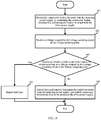
- FIG. 11 A specific flow of the load state detection method is shown in FIG. 11 .
- step 101 the load to be tested is connected with the detecting power supply by controlling the switch unit, before the load to be tested is conductively connected with the drive power supply.
- the microcontroller 4 connects the load 5 to be tested with the detecting power supply 1 by controlling the switch unit 3, before conductively connecting the load 5 to be tested with the drive power supply 6, i.e., before powering on the load 5 to be tested.
- step 102 a voltage sampled by the voltage sampling circuit at the voltage sampling point is received.
- the voltage sampling circuit 2 may sample a voltage at the voltage sampling point T, and output the voltage to the microcontroller 4.
- the microcontroller 4 receives the voltage sampled by the voltage sampling circuit 2 at the voltage sampling point T.
- step 103 it is determined whether a fault exists in the load to be tested according to the voltage sampled by the voltage sampling circuit at the voltage sampling point. If a fault exists, a step 104 will be performed. If no fault exists, a step 105 will be performed.
- the load state detection circuit in FIG. 2 is taken as an example.
- V T is equal to zero
- the microcontroller 4 determines that a grounding short circuit fault occurs to the low-side of the load 5 to be tested. Due to the ADC sampling error, transmission line impedance, software calculation error and so on, the fluctuation value V b may be preset, and when V T ⁇ V b , it may be determined that a grounding short circuit occurs to the low-side of the load 5 to be tested. If a fault exists, the microcontroller 4 needs to determine whether to conductively connect the drive power supply 6 with the load 5 to be tested according to the type of the load to be tested and the fault type of the load 5 to be tested, and the step 104 will be performed. If no fault exists, the step 105 will be performed.
- the microcontroller 4 is further configured to disconnect the load 5 to be tested from the detecting power supply 1 by controlling the switch unit 3, and then determine whether the load 5 to be tested and the drive power supply 6 are short-circuited according to whether the received voltage at the voltage sampling point T is a voltage of the drive power supply 6, before conductively connecting the load 5 to be tested with the drive power supply 6.
- the microcontroller 4 disconnects the detecting power supply 1 from the low-side of the load 5 to be tested by controlling the switch unit 3, and the ADC in the microcontroller 4 samples the voltage V T at the voltage sampling point T. The microcontroller 4 determines that the load 5 to be tested and the drive power supply 6 are short-circuited when V T is equal to the voltage of the drive power supply 6 or fluctuates within a certain range of the voltage of the drive power supply 6.
- step 104 the fault type is reported.
- the microcontroller 4 reports the fault type to a superior controller.
- step 105 the switch unit is controlled to disconnect the load to be tested from the detecting power supply and the conductive connection between the load to be tested and the drive power supply is controlled.
- the microcontroller 4 controls the switch unit 3 to disconnect the load 5 to be tested from the detecting power supply 1 to avoid affecting normal operation of the load 5 to be tested.
- the microcontroller 4 further controls the conductive connection between the load 5 to be tested and the drive power supply 6, that is, the microcontroller 4 controls the high-side drive unit 7 and the low-side drive unit 8 to switch on to power on the load 5 to be tested.
- the steps 101 to 104 is a one-time load state detection flow, and the load 5 to be tested is powered on if no fault exists after the one-time detection of the load 5 to be tested, to which this disclosure is not limited, but the load 5 to be tested is powered on if no fault exists after a plurality of times of detections of the load 5 to be tested.
- the load state detection methods may correspond to the load state detection circuits abovementioned, thus several load state detection methods may be set in view of the load state detection circuits. Relevant technical details in the load state detection circuits are still effective in the load state detection methods and the technical effects that may be achieved in the load state detection circuits may be achieved in the load state detection methods, which will not be repeated here to avoid repetition. Correspondingly, relevant technical details in the load state detection methods may also be applied to the load state detection circuits.
- the load to be tested and the detecting power supply are connected by controlling the switch unit.
- a voltage at the voltage sampling point (the voltage sampling point is formed at either terminal of the load to be tested) is sampled by the voltage sampling circuit, it is determined whether a fault exists in the load to be tested according to the received voltage at the voltage sampling point, and when it is determined that no fault exists in the load to be tested, the load to be tested is disconnected from the detecting power supply by controlling the switch unit, so as to avoid interference of the detecting power supply and then the load to be tested is powered on.
- the load to be tested before the load to be tested is powered on, it is possible to determine in advance whether a fault exists in the load to be tested.
- the load to be tested will not be powered on until it is determined that no fault exists in the load to be tested, thereby safety is improved.
Landscapes
- Physics & Mathematics (AREA)
- General Physics & Mathematics (AREA)
- Engineering & Computer Science (AREA)
- Computer Hardware Design (AREA)
- Microelectronics & Electronic Packaging (AREA)
- Chemical & Material Sciences (AREA)
- Combustion & Propulsion (AREA)
- Testing Of Short-Circuits, Discontinuities, Leakage, Or Incorrect Line Connections (AREA)
Abstract
Description
- The present disclosure relates to the field of circuit technology, especially a load state detection circuit and a load state detection method.
- With the development of battery technologies, it has become a trend in the automotive industry that electric vehicles are replacing fuel vehicles. Some high-power switch devices such as relays, contactors and some loads are applied in electric vehicles, and are important for safe operation of an entire vehicle.
- Some embodiments of the present disclosure provides a load state detection circuit including at least a detecting power supply, a voltage sampling circuit, a switch unit, and a microcontroller. The microcontroller is connected to the switch unit which is connected between the detecting power supply and the load to be tested. A voltage sampling point is formed at either terminal of the load to be tested, and the voltage sampling circuit is connected between the voltage sampling point and the microcontroller. The voltage sampling circuit is configured to sample a voltage at the voltage sampling point, and output the voltage to the microcontroller. The microcontroller is configured to connect the load to be tested and the detecting power supply by controlling the switch unit, and determine whether a fault exists in the load to be tested according to a received voltage at the voltage sampling point sampled by the voltage sampling circuit, before conductively connecting the load to be tested with the drive power supply. The microcontroller is further configured to disconnect the load to be tested from the detecting power supply and control conduction between the load to be tested and the drive power supply by controlling the switch unit when it is determined that no fault exists in the load to be tested.
- Some embodiments of the present disclosure further provides a load state detection method applied to a microcontroller of a load state detection circuit including at least a detecting power supply, a voltage sampling circuit, a switch unit, and a microcontroller. Before conductively connecting the load to be tested with the drive power supply, the load to be tested is connected with the detecting power supply by controlling the switch unit, a voltage sampled by the voltage sampling circuit at the voltage sampling point is received, and it is determined whether a fault exists in the load to be tested according to a voltage sampled by the voltage sampling circuit at the voltage sampling point. The switch unit is controlled to disconnect the load to be tested from the detecting power supply and control conduction between the load to be tested and the drive power supply, when it is determined that no fault exists in the load to be tested.
- In these embodiments, compared with the existing technologies, before the load to be tested is conductively connected with the drive power supply, i.e., before powering on the load to be tested, the load to be tested and the detecting power supply are connected by controlling the switch unit. At this time, a voltage at the voltage sampling point (the voltage sampling point is formed at either terminal of the load to be tested) is sampled by the voltage sampling circuit, it is determined whether a fault exists in the load to be tested according to the received voltage at the voltage sampling point, and when it is determined that no fault exists in the load to be tested, the load to be tested is disconnected from the detecting power supply by controlling the switch unit, so as to avoid interference of the detecting power supply, and power on the load to be tested. In the present disclosure, before the load to be tested is powered on, it is possible to determine in advance whether a fault exists in the load to be tested. The load to be tested will not be powered on until it is determined that no fault exists in the load to be tested, thereby safety is improved.
- Further, the microcontroller is configured to disconnect the load to be tested from the detecting power supply by controlling the switch unit, and determine whether the load to be tested and the drive power supply are short-circuited according to whether the received voltage at the voltage sampling point is a voltage of the drive power supply, before conductively connecting the load to be tested with the drive power supply. This embodiment provides a specific implementation of how to determine whether a load to be tested and a drive power supply are short-circuited.
- Further, the load state detection circuit further includes a first voltage divider circuit. The switch unit is connected to a first terminal of the first voltage divider circuit, a second terminal of the first voltage divider circuit is connected to an terminal of the load to be tested, and a third terminal of the first voltage divider circuit is grounded. In this embodiment, the first voltage divider circuit arranged at the voltage sampling point prevents the voltage sampled by the voltage sampling circuit from being too high to damage the microcontroller.
- Further, the first voltage divider circuit includes a first resistor network and a second resistor network. The switch unit is connected to one terminal of the first resistor network, the other terminal of the first resistor network is connected to an terminal of the second resistor network, and the other terminal of the second resistor network is grounded. The one terminal of the first resistor network forms the first terminal of the first voltage divider circuit. A junction of the first resistor network and second resistor network is connected to a terminal of the load to be tested where the voltage sampling point is formed. The junction of the first resistor network and second resistor network forms the second terminal of the first voltage divider circuit. This embodiment provides a specific structure of a voltage divider circuit.
- Further, the switch unit is a first switch whose control terminal is connected to the microcontroller, one terminal of the first switch is connected to at least one detecting power supply, the other terminal of the first switch is connected to the first terminal of the first voltage divider circuit, and the second terminal of the first voltage divider circuit is connected to an terminal of the load to be tested where the voltage sampling point is formed. The microcontroller is specifically configured to control the first switch to switch on, determine that a grounding short circuit fault occurs to an terminal of the load to be tested where the voltage sampling point is formed when the received voltage at the voltage sampling point is equal to zero, and determine that a grounding short circuit fault occurs to an terminal of the load to be tested where no voltage sampling point is formed when the received voltage at the voltage sampling point is within a first preset range. This embodiment provides an implementation of determining a specific fault type of the load to be tested when the switch unit is the first switch and the second terminal of the first voltage divider circuit is connected to a terminal of the load to be tested where a voltage sampling point is formed.
- Further, the switch unit is the first switch whose control terminal is connected to the microcontroller, one terminal of the first switch is connected to at least one detecting power supply, the other terminal of the first switch is connected to the first terminal of the first voltage divider circuit, and the second terminal of the first voltage divider circuit is connected to an terminal of the load to be tested where no voltage sampling point is formed. The microcontroller is specifically configured to control the first switch to switch on, and determine that a fault occurs to the load to be tested when the received voltage at the voltage sampling point is equal to zero. This embodiment provides an implementation of determining whether a fault exists in the load to be tested when the switch unit is the first switch and the second terminal of the first voltage divider circuit is connected to an terminal of the load to be tested where no voltage sampling point is formed.
- Further, the switch unit includes a second switch and a third switch. A control terminal of the second switch and a control terminal of the third switch are respectively connected to the microcontroller, the load state detection circuit further includes a second voltage divider circuit. A first terminal of the second switch and a first terminal of the third switch are respectively connected to the at least one detecting power supply, a second terminal of the second switch is connected to the first terminal of the first voltage divider circuit, a second terminal of the third switch is connected to a first terminal of the second voltage divider circuit, the second terminal of the first voltage divider circuit and a second terminal of the second voltage divider circuit are connected to two terminals of the load to be tested, respectively, and a third terminal of the second voltage divider circuit is grounded. The microcontroller is specifically configured to control the second switch to switch on, determine that a grounding short circuit fault occurs to an terminal of the load to be tested where the voltage sampling point is formed when the received voltage at the voltage sampling point is equal to zero, and determine that a grounding short circuit fault occurs to an terminal of the load to be tested where no voltage sampling point is formed when the received voltage at the voltage sampling point is within the first preset range. This embodiment provides an implementation of determining a specific fault type of the load to be tested when the switch unit includes the second switch and third switch.
- Further, the microcontroller is configured to control the second switch to switch off and the third switch to switch on, and determine that an open circuit fault occurs to the load to be tested when the received voltage at the voltage sampling point is equal to zero. This embodiment provides a specific implementation of determining whether an open-circuit fault occurs to the load to be tested.
- Further, there are two detecting power supplies, one of which is connected to the first terminal of the second switch, while the other is connected to the first terminal of the third switch.
- Further, the voltage sampling circuit includes a filter unit and an analog-to-digital converter. A first terminal of the analog-to-digital converter is connected to the voltage sampling point via the filter unit, while a second terminal of the analog-to-digital converter is connected to the microcontroller. This embodiment provides a specific structure of a voltage sampling circuit.
- Further, the load state detection circuit includes at least one anti-reverse diode, and at least one terminal of the load to be tested is connected to the switch unit via the at least one anti-reverse diode. In this embodiment, an anti-reverse diode is arranged between the detecting power supply and the load to be tested to avoid countercurrent, which protects the detection circuit, and prevents a detecting loop from being interfered, which may have affected judgment on a fault of the load to be tested.
- Further, a resistance value of the first resistor network and second resistor network is greater than an internal resistance of the load to be tested. This embodiment may prevent the detecting power supply from powering on the load to be tested during detection, which may achieve testing the load to be tested in a case where the detecting power supply has not power on the load to be tested.
- One or more embodiments are described as examples with reference to the corresponding figures in the accompanying drawings, and the examples do not constitute a limitation to the embodiments. Elements with the same reference numerals in the accompanying drawings represent similar elements. The figures in the accompanying drawings do not constitute a proportion limitation unless otherwise stated.
-
FIG. 1 is a structural diagram of a load state detection circuit according to the present disclosure; -
FIG. 2 is a structural diagram of the load state detection circuit according to the present disclosure, wherein a detecting power supply is connected to a low-side of a load to be tested; -
FIG. 3 is a structural diagram of the load state detection circuit according to the present disclosure, wherein the detecting power supply is connected to a high-side of the load to be tested; -
FIG. 4 is a structural diagram of a load state detection circuit according to the present disclosure, wherein detecting power supplies are connected to two terminals of the load to be tested, respectively; -
FIG. 5 is a structural diagram of a load state detection circuit according to the present disclosure; -
FIG. 6 is a structural diagram of a load state detection circuit according to the present disclosure, wherein a second terminal of a first voltage divider circuit is connected to an terminal of the load to be tested where a voltage sampling point is formed; -
FIG. 7 is a structural diagram of a load state detection circuit according to the present disclosure, wherein the second terminal of the first voltage divider circuit is connected to an terminal of the load to be tested where no voltage sampling point is formed; -
FIG. 8 is a structural diagram of a load state detection circuit according to the present disclosure, wherein there are two loads to be tested; -
FIG. 9 is a structural diagram of a load state detection circuit according to the present disclosure; -
FIG. 10 is a structural diagram of a load state detection circuit according to the present disclosure; wherein there are two loads to be tested; -
FIG. 11 is a detailed flowchart of a load state detection method according to the present disclosure. - The embodiments of the present disclosure will be described in detail below with reference to the accompanying drawings in order to make the objectives, technical solutions and advantages of the present disclosure clearer. However, it will be apparent to those skilled in the art that, in the various embodiments of the present disclosure, numerous technical details are set forth in order to provide the reader with a better understanding of the present application. However, the technical solutions claimed in the present application may be implemented without these technical details and various changes and modifications based on the following embodiments.
- The inventor finds that at least the following problems exist in the existing technologies: due to complicated driving conditions and life span of loads per se, failures may occur to high-power switch devices causing dangers.
- Nowadays, after a high-power switch device is powered on, its drive circuit has corresponding protection functions, such as over-temperature protection and over-current protection. However, these are passive protection means that will not work until the device is powered on.
- In view of the above, some embodiments of the present disclosure relates to a load state detection circuit for detecting whether a fault exists in a load to be tested. The load to be tested may be a load in an electric vehicle, such as a relay, a water pump, a valve and so on, and the load to be tested is powered on by a drive power supply. The drive power supply may be a drive power supply of the electric vehicle. However, the present disclosure is not limited hereto, but it may otherwise be another power supply in the electric vehicle. With reference to
FIGs. 1 to 3 , the load state detection circuit includes at least one detectingpower supply 1, avoltage sampling circuit 2, aswitch unit 3 and amicrocontroller 4. - The
microcontroller 4 is connected to theswitch unit 3 which is connected between the detecting power supply and a terminal of aload 5 to be tested. That is, one terminal of theswitch unit 3 is connected to the detectingpower supply 1, while the other terminal of theswitch unit 3 is connected to a terminal of the load to be tested. A voltage sampling point T is formed at either terminal of theload 5 to be tested. Thevoltage sampling circuit 2 is connected between the voltage sampling point T and themicrocontroller 4. - The
voltage sampling circuit 2 is configured to sample a voltage at the voltage sampling point T, and output the voltage to themicrocontroller 4. In one example, thevoltage sampling circuit 2 includes afilter unit 21 and an analog-to-digital converter 22, wherein a first terminal of the analog-to-digital converter 22 is connected to the voltage sampling point T via thefilter unit 21, while a second terminal of the analog-to-digital converter 22 is connected to themicrocontroller 4. An interference signal in the voltage at the voltage sampling point T is filtered by thefilter unit 21 to improve accuracy of the voltage sampled by the analog-to-digital converter 22. In this embodiment, thefilter unit 21 may be a capacitor. During detection, it may select an appropriate delay time according to charge and discharge time of the capacitor for detection. - In one example, an analog-to-digital converter ADC inside the
microcontroller 4 may be used as the analog-to-digital converter 22 of thevoltage sampling circuit 2. However, the present disclosure is not limited hereto, but other sampling chip may otherwise be used as thevoltage sampling circuit 2. - The
microcontroller 4 is configured to connect theload 5 to be tested and the detectingpower supply 1 by controlling theswitch unit 3, and determine whether a fault exists in theload 5 to be tested according to a received voltage at the voltage sampling point T sampled by thevoltage sampling circuit 2, before conductively connecting theload 5 to be tested and thedrive power supply 6. The conduction of thedrive power supply 6 with theload 5 to be tested is simultaneously controlled by a high-side drive unit 7 and a low-side drive unit 8. Thedrive power supply 6 is connected to a high-side of theload 5 to be tested via the high-side drive unit 7. A low-side of theload 5 to be tested is grounded via the low-side drive unit 8. It shall be noted that, in this embodiment and the following embodiments, theload 5 to be tested is conductively connected with thedrive power supply 6, means that, the drive power supply powers theload 5 to be tested on. The "power on (or conductively connect)" herein refers to that the drive power supply provides enough large current and drive theload 5 to be tested to work. That theload 5 to be tested is connected with the detectingpower supply 1 means theload 5 to be tested is electrically connected with the detectingpower supply 1 but the detectingpower supply 1 does not power on theload 5 to be tested; herein, the detectingpower supply 1 is electrically connected with theload 5 to be tested, but provides small current not enough for driving theload 5 to be tested to work. - In one example, the load state detection circuit further includes at least an anti-reverse diode D1. At least one terminal is connected to the switch unit via at least the anti-reverse diode D1 to avoid countercurrent and protect the detection circuit. Besides, a detecting loop is prevented from being interfered, thereby judgment on a fault of the
load 5 to be tested is not affected. - The
microcontroller 4 is further configured to control conduction between theload 5 to be tested and thedrive power supply 6, and disconnect theload 5 to be tested from the detecting power supply by controlling theswitch unit 3, when it is determined that no fault exists in theload 5 to be tested. - It shall be noted that, in this context, connection relationships between the
microcontroller 4 and the three of theswitch unit 3, the high-side drive unit 7 and the low-side drive unit 8 are not embodied in the drawings to maintain clearness of the figures. However, theswitch unit 3, the high-side drive unit 7, and the low-side drive unit 8 are all controlled by themicrocontroller 4. -
FIGs. 2 and3 will be taken as examples for a detailed description of a way in which a load state detection circuit determines a fault of aload 5 to be tested. - With reference to
FIG. 2 , adrive power supply 6 is connected to the high-side of theload 5 to be tested via a high-side drive unit 7, and a low-side of theload 5 to be tested is grounded via a low-side drive unit 8. Themicrocontroller 4 outputs a control signal to control the high-side drive unit 7 and the low-side drive unit 8. There is one detectingpower supply 1. The detectingpower supply 1 is connected to theswitch unit 3, and theswitch unit 3 is connected to the low-side of theload 5 to be tested via the anti-reverse diode D1. The voltage sampling point T is formed at the low-side of theload 5 to be tested. A first terminal of thefilter unit 21 is connected to the voltage sampling point T, and a second terminal of thefilter unit 21 is connected to an ADC in themicrocontroller 4. It shall be noted that, in this context, that the voltage sampling point T is formed at the low-side of theload 5 to be tested is taken as an example for description, to which the present disclosure is not limited, but the voltage sampling point T may otherwise be formed at the high-side of theload 5 to be tested. The high-side of theload 5 to be tested refers to the terminal connected to the positive electrode of thedrive power supply 6, and the low-side of theload 5 to be tested refers to the terminal connected to the negative electrode of thedrive power supply 6. It shall be noted that grounding in the context means being connected to the detectingpower supply 1 and the negative electrode of thedrive power supply 6. - The
microcontroller 4 connects the detectingpower supply 1 and the low-side of theload 5 to be tested by controlling theswitch unit 3. The ADC in themicrocontroller 4 samples a voltage VT at the voltage sampling point T. Themicrocontroller 4 determines that a grounding short circuit fault occurs to the low-side of theload 5 to be tested when VT is equal to zero. It shall be noted that, in practice, due to an ADC sampling error, a transmission line impedance, a software calculation error and so on, a fluctuation value Vb may be preset, and when VT < Vb, it may be determined that a grounding short circuit occurs to the low-side of theload 5 to be tested. - With reference to
FIG. 3 , thedrive power supply 6 is connected to the high-side of theload 5 to be tested via the high-side drive unit 7, and the low-side of theload 5 to be tested is grounded via the low-side drive unit 8. Themicrocontroller 4 outputs a control signal to control the highside drive unit 7 and the lowside drive unit 8. There is one detectingpower supply 1. The detectingpower supply 1 is connected to the anti-reverse diode D1 which is connected to the high-side of theload 5 to be tested via theswitch unit 3. A voltage sampling point T is formed at the low-side of theload 5 to be tested. The first terminal of thefilter unit 21 is connected to the voltage sampling point T, and the second terminal of thefilter unit 21 is connected to the ADC in themicrocontroller 4. - The
microcontroller 4 connects the detectingpower supply 1 with the high-side of theload 5 to be tested by controlling theswitch unit 3. The ADC in themicrocontroller 4 samples the voltage VT at the voltage sampling point T. Themicrocontroller 4 determines that a fault occurs to theload 5 to be tested when VT is equal to a theoretical value zero or fluctuates within a certain range of the theoretical value zero. - In one example, in this embodiment, the
microcontroller 4 is further configured to disconnect theload 5 to be tested from the detectingpower supply 1 by controlling theswitch unit 3, and determine whether theload 5 to be tested and thedrive power supply 6 are short-circuited according to whether the received voltage at the voltage sampling point T is a voltage of thedrive power supply 6, before conductively connecting theload 5 to be tested with thedrive power supply 6. TakeFIG. 2 as an example. Themicrocontroller 4 disconnects the detectingpower supply 1 from the low-side of theload 5 to be tested by controlling theswitch unit 3, and the ADC in themicrocontroller 4 samples the voltage VT at the voltage sampling point T. Themicrocontroller 4 determines that theload 5 to be tested and thedrive power supply 6 are short-circuited when VT is equal to the voltage of thedrive power supply 6 or fluctuates within a certain range of the voltage of thedrive power supply 6. - It shall be noted that,
FIGs. 2 and3 may be combined to form a load state detection circuit as shown inFIG. 4 where there are two detectingpower supplies 1 and twoswitch units 3. The two detectingpower supplies 1 are connected to the anti-reverse diode D1 and the anti-reverse diode D2 via twoswitch unit 3, respectively. The anti-reverse diode D1 and the anti-reverse diode D2 are connected to two terminals of theload 5 to be tested, respectively. The voltage sampling point T may be formed at the high-side or low-side of theload 5 to be tested (the figure takes forming a low terminal of theload 5 as an example), so as to implement all detection functions ofFIGs. 2 and3 as described above. The two detectingpower supplies 1 may be identical or different, to which this disclosure does not impose any limitation. - It shall further be noted that when the detecting
power supply 1 is only connected to one terminal of theload 5 to be tested, the anti-reverse diode may not be provided, to which this disclosure does not impose any limitation. - In this disclosure, compared with the existing technologies, before the load to be tested and the drive power supply are powered on, i.e., before powering on the load to be tested, the load to be tested and the detecting power supply are connected by controlling the switch unit. At this time, a voltage at the voltage sampling point (the voltage sampling point is formed at either terminal of the load to be tested) is sampled by the voltage sampling circuit, it is determined whether a fault exists in the load to be tested according to the received voltage at the voltage sampling point, and when it is determined that no fault exists in the load to be tested, the load to be tested is disconnected from the detecting power supply by controlling the switch unit so as to avoid interference of the detecting power supply, and power on the load to be tested. In the present disclosure, before the load to be tested is powered on, it is possible to determine in advance whether a fault exists in the load to be tested. The load to be tested will not be powered on until it is determined that no fault exists in the load to be tested, thereby safety is improved.
- With reference to
FIG. 5 , the load state detection circuit further includes a firstvoltage divider circuit 10. - The
switch unit 3 is connected to a first terminal of the firstvoltage divider circuit 10. A second terminal of the firstvoltage divider circuit 10 is connected to theload 5 to be tested. A third terminal of the firstvoltage divider circuit 10 is grounded. - In one example, the first
voltage divider circuit 10 includes a first resistor network and a second resistor network. Theswitch unit 3 is connected to one terminal of the first resistor network, and the other terminal of the first resistor network is connected to a terminal of the second resistor network. The one terminal of the first resistor network forms the first terminal of the firstvoltage divider circuit 10. A junction K of the first resistor network and second resistor network forms the second terminal of the firstvoltage divider circuit 10, and the other terminal of the second resistor network forms the third terminal of the firstvoltage divider circuit 10. It shall be noted that in this context, that the first resistor network is a first resistor R1 and the second resistor network is a second resistor R2 is taken as an example for description, but this disclosure does not impose any limitation to the specific structures of the first resistor network and the second resistor network. - Take
FIG. 5 as an example for description. There is one detectingpower supply 1. The detectingpower supply 1 is connected to the first terminal of the firstvoltage divider circuit 10 via theswitch unit 3, and the second terminal of the firstvoltage divider circuit 10 is connected to the low-side of theload 5 to be tested, and the voltage sampling point T is formed at the low-side of theload 5 to be tested. - In one example, a resistance value of the first resistor network and a resistance value of the second resistor network are greater than an internal resistance r of the
load 5 to be tested. In one example, the resistance value of the first resistor R1 and the resistance value of the second resistor R2 are ten times the internal resistance r of theload 5 to be tested, thereby reducing current in the circuit when performing detection. While, generally, large current is needed when powering on theload 5 to be tested. That is, theload 5 to be tested is detected in a case when the detectingpower supply 1 does not power on theload 5 to be tested. - In this way, the first voltage divider circuit arranged at the voltage sampling point prevents the voltage sampled by the voltage sampling circuit from being too high to damage the microcontroller. Besides, a specific structure of the first voltage divider circuit is provided.
- With reference to
FIG. 6 , it is provided a specific way of determining a fault in the load to be tested when theswitch unit 3 is a first switch K1. - The
switch unit 3 is the first switch K1 whose control terminal is connected to themicrocontroller 4. Themicrocontroller 4 may control switch on and switch off of the first switch K1. One terminal of the first switch K1 is connected to the detectingpower supply 1, and the other terminal of the first switch K1 is connected to the first terminal of the firstvoltage divider circuit 10. - When the second terminal of the first
voltage divider circuit 10 is connected to an terminal of the load to be tested where a voltage sampling point is formed, with reference toFIG. 6 , themicrocontroller 4 is specifically configured to control the first switch K1 to switch on and receive the sampled voltage VT by the ADC at the voltage sampling point T. When VT is equal to zero, themicrocontroller 4 determines that a grounding short circuit fault occurs to the terminal of theload 5 to be tested where the voltage sampling point T is formed, that is, a grounding short circuit occurs to the low-side of theload 5 to be tested as shown inFIG. 6 . - When VT is within a first preset range, the
microcontroller 4 determines that a grounding short circuit fault occurs to the terminal of theload 5 to be tested where the voltage sampling point T is not formed, that is, the grounding short circuit fault occurs to the high-side of theload 5 to be tested as shown inFIG. 6 . The first preset range shall be set according to the first resistor R1, the second resistor R2, the internal resistance r of theload 5 to be tested, and the voltage V of the detecting power supply. Specifically, suppose a grounding short circuit fault occurs to the high-side of theload 5 to be tested, then a theoretical value of the voltage VT at the voltage sampling point T is V*r*R2/(r *R2+R1* r +R1*R2). If a fluctuation value Vb1 is preset on the basis of the theoretical value, it may be obtained that the first preset range is [V*r*R2/(r *R2+R1* r +R1*R2)-Vb1, V*r*R2/(r *R2+R1* r +R1*R2)+ Vb1], - When the second terminal of the first
voltage divider circuit 10 is connected to an terminal of the load to be tested where the voltage sampling point is not formed, with reference toFIG. 7 , themicrocontroller 4 is specifically configured to control the first switch K1 to switch on. When the received voltage VT at the voltage sampling point T is equal to the theoretical value zero, or fluctuates within a certain range of the theoretical value zero, it is determined that a fault occurs to theload 5 to be tested. - Before controlling the first switch K1 to switch on, the
microcontroller 4 determines whether theload 5 to be tested and thedrive power supply 6 are short-circuited by controlling the first switch K1 to disconnect theload 5 to be tested from the detectingpower supply 1 and according to whether the received voltage at the voltage sampling point T is a voltage of thedrive power supply 6. TakeFIG. 6 for example, where themicrocontroller 4 controls the first switch K1 to disconnect the detectingpower supply 1 from the low-side of theload 5 to be tested. It is determined that theload 5 to be tested and thedrive power supply 6 are short-circuited if the voltage VT at the voltage sampling point T sampled by the ADC of themicrocontroller 4 is equal to the a theoretical value VQ*(R2/(r+R2)) or fluctuates within a certain range of the theoretical value VQ*(R2/(r+R2)). VQ represents a voltage of thedrive power supply 6, and r represents an internal resistance of theload 5 to be tested. - It shall be noted that the load state detection circuit of the disclosure may further test a plurality of
loads 5 to be tested at the same time. With reference toFIG. 8 , that there are twoloads 5 to be tested is taken as an example. The way to determine a fault of the each of theloads 5 to be tested is similar to the above described, and will not be repeated here. Therefore, themicrocontroller 4 may determine whether to power on theloads 5 to be tested according to types of the loads and fault statuses of the loads, which is more secure. - In view of the above, it is provided an implementation manner of determining a specific fault type of the load to be tested when the switch unit is the first switch.
- With reference to
FIG. 9 , it is provided a specific way of determining a fault in the load to be tested when theswitch unit 3 includes a second switch K2 and a third switch K3. - The
switch unit 3 includes the second switch K2 and the third switch K3. Control terminals of the second switch K2 and the third switch K3 are respectively connected to themicrocontroller 4. The load state detection circuit further includes a secondvoltage divider circuit 20 whose structure may be similar to that of the firstvoltage divider circuit 10. Specifically, the secondvoltage divider circuit 20 includes a third resistor network and a fourth resistor network. One terminal of the third resistor network forms a first terminal of the secondvoltage divider circuit 20, the other terminal of the third resistor network is connected to one terminal of the fourth resistor network. The other terminal of the fourth resistor network is grounded. A junction M of the third resistor network and the fourth resistor network forms a second terminal of the secondvoltage divider circuit 20. The second terminal of the secondvoltage divider circuit 20 is connected to one terminal of theload 5 to be tested. It shall be noted that, in this context, that the third resistor network is a third resistor R3 and the fourth resistor network is a fourth resistor R4 is taken as an example for description. However, this disclosure does not impose any limitation to the specific structures of the third resistor network and fourth resistor network. - A first terminal of the second switch K2 and a first terminal of the third switch K3 are respectively connected to at least one detecting
power supply 1. A second terminal of the second switch K2 is connected to the first terminal of the firstvoltage divider circuit 10. A second terminal of the third switch K3 is connected to the first terminal of the secondvoltage divider circuit 20. The second terminal of the firstvoltage divider circuit 10 and the second terminal of the secondvoltage divider circuit 20 are connected to two terminals (high-side and low-side) of theload 5 to be tested, respectively. There may be two detectingpower supplies 1, one of which is connected to the first terminal of the second switch K2, while the other detectingpower supply 1 is connected to the first terminal of the third switch K3. In this embodiment, the two detectingpower supplies 1 may be identical or different, to which this disclosure does not impose any limitation. - As shown in
FIG. 9 , the firstvoltage divider circuit 10 includes the first resistor network and the second resistor network. The first resistor network is the first resistor R1, and the second resistor network is the second resistor R2. One detectingpower supply 1 is connected to a terminal of the second switch K2. The other terminal of the second switch K2 is connected to a terminal of the first resistor R1 of the firstvoltage divider circuit 10 via the anti-reverse diode D1. The other terminal of the first resistor R1 is connected to one terminal of the second resistor R2. The other terminal of the second resistor R2 is grounded. The junction K of the first resistor R1 and second resistor forms the second terminal of the firstvoltage divider circuit 10. The second terminal of the firstvoltage divider circuit 10 is connected to an terminal of theload 5 to be tested where the voltage sampling point T is formed, i.e., the low-side of theload 5 to be tested. The other detectingpower supply 1 is connected to a terminal of the third switch K3, the other terminal of which is connected to one terminal of the third resistor R3 of the secondvoltage divider circuit 20 via the anti-reverse diode D2. The other terminal of the third resistor R3 is connected to one terminal of the fourth resistor R4. The other terminal of the fourth resistor R4 is grounded. The junction M of the third resistor R3 and the fourth resistor R4 form the second terminal of the secondvoltage divider circuit 20. The second terminal of the secondvoltage divider circuit 20 is connected to an terminal of theload 5 to be tested where the voltage sampling point T is not formed, i.e., the high-side of theload 5 to be tested. - Specifically, the
microcontroller 4 is configured to control the second switch K2 to switch on and receive the voltage VT sampled by the ADC at the voltage sampling point T. When VT is equal to zero, themicrocontroller 4 determines that a grounding short circuit fault occurs to a terminal of theload 5 to be tested where the voltage sampling point T is formed, that is, a grounding short circuit fault occurs to the low-side of theload 5 to be tested as shown inFIG. 9 . It shall be noted that, in practice, due to the ADC sampling error, transmission line impedance, software calculation error and so on, the fluctuation value Vb may be preset, and when VT < Vb, it may be determined that a grounding short circuit occurs to the low-side of theload 5 to be tested. - When VT is within a first preset range, the
microcontroller 4 determines that a grounding short circuit fault occurs to the terminal of theload 5 to be tested where the voltage sampling point T is not formed, that is, the grounding short circuit fault occurs to the high-side of theload 5 to be tested as shown inFIG. 9 . The first preset range shall be set according to the first resistor network, the second resistor network, the internal resistance r of theload 5 to be tested, and the voltage V of the detecting power supply. Specifically, suppose a grounding short circuit fault occurs to the high-side of theload 5 to be tested, then the theoretical value of the voltage VT at the voltage sampling point T is V*r*R2/(r *R2+R1* r +R1*R2). If a fluctuation value Vb1 is preset on the basis of the theoretical value, it may be obtained that the first preset range is [V*r*R2/(r *R2+R1* r +R1*R2)- Vb1, V*r*R2/(r *R2+R1* r +R1*R2)+ Vb1]. Causes of a fluctuation value include but are not limited to a resistor error in the circuit, an ADC sampling error, a detecting power supply error, a drive power supply error, a transmission line impedance, and software computation error and the like. - The
microcontroller 4 is further configured to control the second switch K2 to switch off and the third switch K3 to switch on, and determine that an open circuit fault occurs to theload 5 to be tested when the received voltage VT at the voltage sampling point T is equal to zero. - Before controlling the second switch K2 and third switch K3 to switch on, the
microcontroller 4 determines whether theload 5 to be tested and thedrive power supply 6 are short-circuited by controlling the second switch K2 and third switch K3 to disconnect theload 5 to be tested from the two detectingpower supplies 1 and according to whether the received voltage at the voltage sampling point T is a voltage of thedrive power supply 6. TakeFIG. 9 for example, where themicrocontroller 4 controls the second switch K2 and third switch K3 to disconnect the two detectingpower supplies 1 from the high-side and low-side of theload 5 to be tested. It is determined that theload 5 to be tested and thedrive power supply 6 are short-circuited if the voltage VT at the voltage sampling point T sampled by the ADC of themicrocontroller 4 is equal to the theoretical value VQ*(R2/(r+R2)) or fluctuates within a certain range of the theoretical value VQ*(R2/(r+R2)). VQ represents a voltage of thedrive power supply 6, and r represents an internal resistance of theload 5 to be tested. - It shall be noted that when controlling the second switch K2 to switch on, the
microcontroller 4 may simultaneously control the third switch K3 to switch on, and then control the second switch K2 to switch off, which may reduce charge and discharge time of the filter unit 21 (capacitor) and thereby reducing the detection delay time, as compared with separately controlling the second switch K2 and the third switch K3 to switch on in sequence. - It shall be noted that the load state detection circuit of the present disclosure may further test a plurality of
loads 5 to be tested at the same time. With reference toFIG. 10 , that there are twoloads 5 to be tested is taken as an example. High-sides of the plurality ofloads 5 to be tested share one detectingpower supply 1, and low-sides of the plurality ofloads 5 to be tested share one detectingpower supply 1. The way to determine the fault of each of theloads 5 to be tested is similar to the above described, and will not be repeated here. Therefore, themicrocontroller 4 may determine whether to power on theloads 5 to be tested according to types of the loads and fault statuses of the loads, which is more secure. - In this way, it is provided an implementation manner of determining a specific fault type of the load to be tested when the switch unit includes the second switch and the third switch.
- The present disclosure further relates to a load state detection method, applied to any load state detection circuit abovementioned. The load state detection circuit with reference to
FIGs. 1 to 3 is taken as an example for description. - A specific flow of the load state detection method is shown in
FIG. 11 . - In
step 101, the load to be tested is connected with the detecting power supply by controlling the switch unit, before the load to be tested is conductively connected with the drive power supply. - Specifically, the
microcontroller 4 connects theload 5 to be tested with the detectingpower supply 1 by controlling theswitch unit 3, before conductively connecting theload 5 to be tested with thedrive power supply 6, i.e., before powering on theload 5 to be tested. - In
step 102, a voltage sampled by the voltage sampling circuit at the voltage sampling point is received. - Specifically, the
voltage sampling circuit 2 may sample a voltage at the voltage sampling point T, and output the voltage to themicrocontroller 4. Themicrocontroller 4 receives the voltage sampled by thevoltage sampling circuit 2 at the voltage sampling point T. - In
step 103, it is determined whether a fault exists in the load to be tested according to the voltage sampled by the voltage sampling circuit at the voltage sampling point. If a fault exists, astep 104 will be performed. If no fault exists, astep 105 will be performed. - Specifically, the load state detection circuit in
FIG. 2 is taken as an example. When VT is equal to zero, themicrocontroller 4 determines that a grounding short circuit fault occurs to the low-side of theload 5 to be tested. Due to the ADC sampling error, transmission line impedance, software calculation error and so on, the fluctuation value Vb may be preset, and when VT < Vb, it may be determined that a grounding short circuit occurs to the low-side of theload 5 to be tested. If a fault exists, themicrocontroller 4 needs to determine whether to conductively connect thedrive power supply 6 with theload 5 to be tested according to the type of the load to be tested and the fault type of theload 5 to be tested, and thestep 104 will be performed. If no fault exists, thestep 105 will be performed. - In one example, the
microcontroller 4 is further configured to disconnect theload 5 to be tested from the detectingpower supply 1 by controlling theswitch unit 3, and then determine whether theload 5 to be tested and thedrive power supply 6 are short-circuited according to whether the received voltage at the voltage sampling point T is a voltage of thedrive power supply 6, before conductively connecting theload 5 to be tested with thedrive power supply 6. TakeFIG. 2 as an example, themicrocontroller 4 disconnects the detectingpower supply 1 from the low-side of theload 5 to be tested by controlling theswitch unit 3, and the ADC in themicrocontroller 4 samples the voltage VT at the voltage sampling point T. Themicrocontroller 4 determines that theload 5 to be tested and thedrive power supply 6 are short-circuited when VT is equal to the voltage of thedrive power supply 6 or fluctuates within a certain range of the voltage of thedrive power supply 6. - In
step 104, the fault type is reported. - Specifically, the
microcontroller 4 reports the fault type to a superior controller. - In
step 105, the switch unit is controlled to disconnect the load to be tested from the detecting power supply and the conductive connection between the load to be tested and the drive power supply is controlled. - Specifically, the
microcontroller 4 controls theswitch unit 3 to disconnect theload 5 to be tested from the detectingpower supply 1 to avoid affecting normal operation of theload 5 to be tested. Themicrocontroller 4 further controls the conductive connection between theload 5 to be tested and thedrive power supply 6, that is, themicrocontroller 4 controls the high-side drive unit 7 and the low-side drive unit 8 to switch on to power on theload 5 to be tested. - It shall be noted that, the
steps 101 to 104 is a one-time load state detection flow, and theload 5 to be tested is powered on if no fault exists after the one-time detection of theload 5 to be tested, to which this disclosure is not limited, but theload 5 to be tested is powered on if no fault exists after a plurality of times of detections of theload 5 to be tested. - In other examples, the load state detection methods may correspond to the load state detection circuits abovementioned, thus several load state detection methods may be set in view of the load state detection circuits. Relevant technical details in the load state detection circuits are still effective in the load state detection methods and the technical effects that may be achieved in the load state detection circuits may be achieved in the load state detection methods, which will not be repeated here to avoid repetition. Correspondingly, relevant technical details in the load state detection methods may also be applied to the load state detection circuits.
- In this disclosure, compared with the existing technologies, before the load to be tested and the drive power supply are conductively connected, i.e., before powering on the load to be tested, the load to be tested and the detecting power supply are connected by controlling the switch unit. At this time, a voltage at the voltage sampling point (the voltage sampling point is formed at either terminal of the load to be tested) is sampled by the voltage sampling circuit, it is determined whether a fault exists in the load to be tested according to the received voltage at the voltage sampling point, and when it is determined that no fault exists in the load to be tested, the load to be tested is disconnected from the detecting power supply by controlling the switch unit, so as to avoid interference of the detecting power supply and then the load to be tested is powered on. In the present disclosure, before the load to be tested is powered on, it is possible to determine in advance whether a fault exists in the load to be tested. The load to be tested will not be powered on until it is determined that no fault exists in the load to be tested, thereby safety is improved.
- Those skilled in the art should appreciate that the aforementioned embodiments are specific embodiments for implementing the present disclosure. In practice, however, many changes can be made in the forms and details of the specific embodiments without departing from the scope of the disclosure.
Claims (15)
- A load state detection circuit, characterized by comprising: at least one detecting power supply (1), a voltage sampling circuit (2), a switch unit (3), and a microcontroller (4);
wherein the microcontroller (4) is connected to the switch unit (3), the switch unit (3) is connected between the detecting power supply (1) and the load (5) to be tested;
wherein a voltage sampling point (T) is formed at either terminal of the load (5) to be tested, and the voltage sampling circuit (2) is connected between the voltage sampling point (T) and the microcontroller (4);
wherein the voltage sampling circuit (2) is configured to sample a voltage at the voltage sampling point (T), and output the voltage to the microcontroller (4);
wherein the microcontroller (4) is configured to, before conductively connecting the load (5) to be tested with the drive power supply (6), electrically connect the load (5) to be tested and the detecting power supply (1) by controlling the switch unit (3), and determine whether a fault exists in the load (5) to be tested according to a received voltage at the voltage sampling point (T) sampled by the voltage sampling circuit (2); and
wherein the microcontroller (4) is further configured to, when it is determined that no fault exists in the load (5) to be tested, disconnect the load (5) to be tested from the detecting power supply (1) by controlling the switch unit (3), and control conductive connection between the load (5) to be tested and the drive power supply (6) to drive the load (5) to be tested to work;
alternately, wherein the microcontroller (4) is further configured to, before conductively connecting the load (5) to be tested with the drive power supply (6), disconnect the load (5) to be tested from the detecting power supply (1) by controlling the switch unit (3), and determine whether the load (5) to be tested and the drive power supply (6) are short-circuited according to whether the received voltage at the voltage sampling point (T) is a voltage of the drive power supply (6). - The load state detection circuit according to claim 1, further comprising: a first voltage divider circuit (10);
wherein the switch unit (3) is connected to a first terminal of the first voltage divider circuit (10), a second terminal of the first voltage divider circuit (10) is connected to an terminal of the load (5) to be tested, and a third terminal of the first voltage divider circuit (10) is grounded. - The load state detection circuit according to claim 2, wherein the first voltage divider circuit (10) comprises a first resistor network and a second resistor network;
wherein the switch unit (3) is connected to one terminal of the first resistor network, and the other terminal of the first resistor network is connected to an terminal of the second resistor network; and
wherein the one terminal of the first resistor network forms the first terminal of the first voltage divider circuit (10), a junction of the first resistor network and the second resistor network forms the second terminal of the first voltage divider circuit (10), and the other terminal of the second resistor network forms the third terminal of the first voltage divider circuit (10). - The load state detection circuit according to claim 2 or 3, wherein the switch unit (3) is a first switch (K1); a control terminal of the first switch (K1) is connected to the microcontroller (4), one terminal of the first switch (K1) is connected to the detecting power supply (1), the other terminal of the first switch (K1) is connected to the first terminal of the first voltage divider circuit (10), and the second terminal of the first voltage divider circuit (10) is connected to an terminal of the load (5) to be tested where the voltage sampling point (T) is formed; and
wherein the microcontroller (4) is specifically configured to control the first switch (K1) to switch on, and determine that a grounding short circuit fault occurs to an terminal of the load (5) to be tested where the voltage sampling point (T) is formed when the received voltage at the voltage sampling point (T) is approximately equal to zero; and the microcontroller (4) is further configured to determine that a grounding short circuit fault occurs to an terminal of the load (5) to be tested where no voltage sampling point (T) is formed when the received voltage at the voltage sampling point (T) is within a first preset range. - The load state detection circuit according to claim 2 or 3, wherein the switch unit (3) is a first switch (K1); a control terminal of the first switch (K1) is connected to the microcontroller (4), one terminal of the first switch (K1) is connected to the detecting power supply (1), the other terminal of the first switch (K1) is connected to the first terminal of the first voltage divider circuit (10), and the second terminal of the first voltage divider circuit (10) is connected to an terminal of the load (5) to be tested where no voltage sampling point (T) is formed; and
wherein the microcontroller (4) is specifically configured to control the first switch (K1) to switch on, and determine that a fault occurs to the load (5) to be tested when the received voltage at the voltage sampling point (T) is approximately equal to zero. - The load state detection circuit according to claim 2 or 3, wherein the switch unit (3) comprises a second switch (K2) and a third switch (K3); wherein a control terminal of the second switch (K2) and a control terminal of the third switch (K3) are respectively connected to the microcontroller (4); the load state detection circuit further comprises a second voltage divider circuit (20);
wherein a first terminal of the second switch (K2) and a first terminal of the third switch (K3) are respectively connected to the at least one detecting power supply (1), a second terminal of the second switch (K2) is connected to the first terminal of the first voltage divider circuit (10), a second terminal of the third switch (K3) is connected to a first terminal of the second voltage divider circuit (20), the second terminal of the first voltage divider circuit (10) and a second terminal of the second voltage divider circuit (20) are connected to two terminals of the load (5) to be tested, respectively, and a third terminal of the second voltage divider circuit (20) is grounded; and
wherein the microcontroller (4) is specifically configured to control the second switch (K2) to switch on, and determine that a grounding short circuit fault occurs to an terminal of the load (5) to be tested where the voltage sampling point (T) is formed when the received voltage at the voltage sampling point (T) is approximately equal to zero; and the microcontroller (4) is further configured to determine that a grounding short circuit fault occurs to an terminal of the load (5) to be tested where no voltage sampling point is formed when the received voltage at the voltage sampling point (T) is within the first preset range. - The load state detection circuit according to claim 6, wherein the microcontroller (4) is further configured to control the second switch (K2) to switch off and the third switch (K3) to switch on, and determine that an open circuit fault occurs to the load (5) to be tested when the received voltage at the voltage sampling point (T) is approximately equal to zero.
- The load state detection circuit according to claim 6 or 7, wherein there are two detecting power supplies, one of which is connected to the first terminal of the second switch (K2), while the other is connected to the first terminal of the third switch (K3).
- The load state detection circuit according to any one of claims 1 to 8, wherein the voltage sampling circuit (2) comprises a filter unit (21) and an analog-to-digital converter;
wherein a first terminal of the analog-to-digital converter is connected to the voltage sampling point (T) via the filter unit (21), while a second terminal of the analog-to-digital converter is connected to the microcontroller (4);
alternately, the load state detection circuit further comprising at least one anti-reverse diode (D1,D2), wherein at least one terminal of the load (5) to be tested is connected to the switch unit (3) via the at least one anti-reverse diode (D1,D2). - The load state detection circuit according to any one of claims 1 to 9, wherein a resistance value of the first resistor network and a resistance value of the second resistor network is greater than an internal resistance of the load (5) to be tested.
- A load state detection method, being applied to a microcontroller (4) of a load state detection circuit according to any one of claims 1 to 12, wherein the method comprises:before conductively connecting the load (5) to be tested with the drive power supply (6), electrically connecting the load (5) to be tested with the detecting power supply (1) by controlling the switch unit (3);receiving a voltage sampled by the voltage sampling circuit (2) at the voltage sampling point (T);determining whether a fault exists in the load (5) to be tested according to the voltage sampled by the voltage sampling circuit (2) at the voltage sampling point (T); andcontrolling the switch unit (3) to disconnect the load (5) to be tested from the detecting power supply (1) and controlling the load (5) to be tested to be conductively connected with the drive power supply (6) to drive the load (5) to be tested to work, when it is determined that no fault exists in the load (5) to be tested.
- The load state detection method according to claim 11, comprising:before conductively connecting the load (5) to be tested with the drive power supply (6), disconnecting the load (5) to be tested with the detecting power supply (1) by controlling the switch unit (3);receiving a voltage sampled by the voltage sampling circuit (2) at the voltage sampling point (T);determining that the load (5) to be tested and the drive power supply (6) are short-circuited, when it is determined that the received voltage at the voltage sampling point (T) is approximately a voltage of the drive power supply (6);controlling the load (5) to be tested to be conductively connected with the drive power supply (6) to drive the load (5) to be tested to work, when it is determined that the load (5) to be tested and the drive power supply (6) are not short-circuited.
- The load state detection method according to claim 11 or 12, especially being applied to the microcontroller (4) of the load state detection circuit according to claim 4, comprising:before conductively connecting the load (5) to be tested with the drive power supply (6), electrically connecting the load (5) to be tested with the detecting power supply (1) by controlling the first switch (K1);receiving a voltage sampled by the voltage sampling circuit (2) at the voltage sampling point (T);determining that a grounding short circuit fault occurs to an terminal of the load (5) to be tested where the voltage sampling point (T) is formed when the received voltage at the voltage sampling point (T) is approximately equal to zero; determining that a grounding short circuit fault occurs to the terminal of the load 5 to be tested where the voltage sampling point T is not formed when the voltage sampled at the voltage sampling point (T) is approximately V*r*R2/(r *R2+R1* r +R1*R2); wherein R1 represents a resistance of the first resistor, R2 represents a resistance of the second resistor, r represents an internal resistance of the load (5) to be tested, V represents a voltage of the detecting power supply (1).
- The load state detection method according to claim 11 or 12, especially being applied to the microcontroller (4) of the load state detection circuit according to claim 5, comprising:before conductively connecting the load (5) to be tested with the drive power supply (6), electrically connecting the load (5) to be tested with the detecting power supply (1) by controlling the first switch (K1);receiving a voltage sampled by the voltage sampling circuit (2) at the voltage sampling point (T);determining that a fault occurs to the load (5) to be tested when the received voltage at the voltage sampling point (T) is approximately equal to zero;electrically disconnecting the load (5) to be tested with the detecting power supply (1) by controlling the first switch (K1);receiving a voltage sampled by the voltage sampling circuit (2) at the voltage sampling point (T);determining that the load (5) to be tested and the drive power supply (6) are short-circuited, when it is determined that the voltage sampled at the voltage sampling point (T) is approximately VQ*(R2/(r+R2)); wherein VQ represents a voltage of the drive power supply (6), r represents an internal resistance of the load (5) to be tested, R2 represents a resistance of the second resistor.
- The load state detection method according to claim 11 or 12, especially being applied to a microcontroller (4) of a load state detection circuit according to claim 6, comprising:before conductively connecting the load (5) to be tested with the drive power supply (6), electrically connecting a low terminal of the load (5) to be tested with the detecting power supply (1) by controlling the second switch (K2), electrically disconnecting a high terminal of the load (5) to be tested with the detecting power supply (1) by controlling the third switch (K3);receiving a voltage sampled by the voltage sampling circuit (2) at the voltage sampling point (T);determining that a grounding short circuit fault occurs to the low terminal of the load (5) to be tested when the received voltage at the voltage sampling point (T) is approximately equal to zero; determining that a grounding short circuit fault occurs to the high terminal of the load (5) to be tested when the voltage sampled at the voltage sampling point (T) is approximately V*r*R2/(r *R2+R1* r +R1*R2); wherein R1 represents a resistance of the first resistor, R2 represents a resistance of the second resistor, r represents an internal resistance of the load (5) to be tested, V represents a voltage of the detecting power supply (1);electrically disconnecting the low terminal of the load (5) to be tested with the detecting power supply (1) by controlling the second switch unit (K2), electrically connecting the high terminal of the load (5) to be tested with the detecting power supply (1) by controlling the third switch (K3);receiving a voltage sampled by the voltage sampling circuit (2) at the voltage sampling point (T);determining that an open fault occurs to the load (5) to be tested when the received voltage at the voltage sampling point (T) is approximately equal to zero;electrically disconnecting the low terminal of the load (5) to be tested with the detecting power supply (1) by controlling the second switch unit (K2), electrically disconnecting the high terminal of the load (5) to be tested with the detecting power supply (1) by controlling the third switch (K3);receiving a voltage sampled by the voltage sampling circuit (2) at the voltage sampling point (T);determining that the load (5) to be tested and the drive power supply (6) are short-circuited, when it is determined that the voltage sampled at the voltage sampling point (T) is approximately VQ*(R2/(r+R2)); wherein VQ represents a voltage of the drive power supply (6), r represents an internal resistance of the load (5) to be tested, R2 represents a resistance of the second resistor.
Applications Claiming Priority (1)
| Application Number | Priority Date | Filing Date | Title |
|---|---|---|---|
| CN201811079845.9A CN110907853B (en) | 2018-09-17 | 2018-09-17 | Load state detection circuit and method |
Publications (2)
| Publication Number | Publication Date |
|---|---|
| EP3623824A1 true EP3623824A1 (en) | 2020-03-18 |
| EP3623824B1 EP3623824B1 (en) | 2021-11-24 |
Family
ID=67439016
Family Applications (1)
| Application Number | Title | Priority Date | Filing Date |
|---|---|---|---|
| EP19188497.2A Active EP3623824B1 (en) | 2018-09-17 | 2019-07-26 | Load state detection circuit and method |
Country Status (3)
| Country | Link |
|---|---|
| US (2) | US10983154B2 (en) |
| EP (1) | EP3623824B1 (en) |
| CN (2) | CN110907853B (en) |
Families Citing this family (10)
| Publication number | Priority date | Publication date | Assignee | Title |
|---|---|---|---|---|
| EP3582584A1 (en) * | 2018-06-12 | 2019-12-18 | Continental Automotive GmbH | Electric circuit and diagnostic method for an electric load |
| CN110907853B (en) | 2018-09-17 | 2021-02-19 | 宁德时代新能源科技股份有限公司 | Load state detection circuit and method |
| CN113253159B (en) * | 2021-03-26 | 2022-12-06 | 浙江高泰昊能科技有限公司 | Battery pack load identification and voltage detection circuit and working method thereof |
| CN113740765B (en) * | 2021-09-03 | 2024-08-06 | 赛尔富电子有限公司 | Short circuit detection circuit |
| US11668761B2 (en) * | 2021-10-06 | 2023-06-06 | Dell Products, L.P. | Adaptive short circuit detection system and method for an information handling system (IHS) |
| CN114333656B (en) * | 2021-12-10 | 2023-12-12 | 北京镁伽科技有限公司 | Power self-checking system, adjustable voltage source and image signal generator |
| CN114646860A (en) * | 2022-02-18 | 2022-06-21 | 深圳拓邦股份有限公司 | Motor drive circuit short circuit detection device and electrical apparatus |
| CN114755510B (en) * | 2022-03-11 | 2025-11-21 | Tcl家用电器(合肥)有限公司 | Household appliance monitoring method |
| CN116599346B (en) * | 2023-07-17 | 2023-10-13 | 广州中基国威电子科技有限公司 | Load driving circuit, method and electronic equipment |
| CN117250475B (en) * | 2023-08-21 | 2025-03-11 | 东风商用车有限公司 | High-side driver fault diagnosis system and method |
Citations (4)
| Publication number | Priority date | Publication date | Assignee | Title |
|---|---|---|---|---|
| DE4338462A1 (en) * | 1993-11-11 | 1995-05-18 | Hella Kg Hueck & Co | Monitoring system for electrical loads in motor vehicles |
| US6056384A (en) * | 1997-10-08 | 2000-05-02 | Honda Giken Kogyo Kabushiki Kaisha | Failure diagnosing circuit and method |
| US20130162261A1 (en) * | 2010-07-01 | 2013-06-27 | Robert Bosch Gmbh | Method and circuit assembly for the diagnosis of a load path in a vehicle |
| CN207036999U (en) * | 2017-07-26 | 2018-02-23 | 重庆海德世拉索系统(集团)有限公司 | Motor terminal abnormal detection circuit |
Family Cites Families (14)
| Publication number | Priority date | Publication date | Assignee | Title |
|---|---|---|---|---|
| JP2542618Y2 (en) * | 1988-08-30 | 1997-07-30 | アルプス電気株式会社 | In-vehicle load condition detection drive |
| DE102006045308B4 (en) * | 2006-09-26 | 2011-07-21 | Continental Automotive GmbH, 30165 | Circuit arrangement for detecting the state of a load device which can be connected to a switching connection and method for operating such a circuit arrangement |
| US20090174413A1 (en) * | 2008-01-03 | 2009-07-09 | Teknic, Inc. | Method and Apparatus to Verify the Proper Connection of Loads before Applying Full DC Power |
| CN103176070B (en) | 2011-12-23 | 2016-06-01 | 比亚迪股份有限公司 | Fault collection circuit and there is its fault diagnosis circuit |
| DE102012013405A1 (en) * | 2012-07-05 | 2014-01-09 | Audi Ag | Diagnostic device for checking a control signal line |
| JP2014091495A (en) * | 2012-11-07 | 2014-05-19 | Toyota Industries Corp | Short-cut detection circuit |
| CN203720299U (en) | 2014-01-21 | 2014-07-16 | 浙江万向亿能动力电池有限公司 | Relay coil driving diagnosis device |
| CN206311669U (en) * | 2016-11-29 | 2017-07-07 | 深圳市沃特玛电池有限公司 | load resistance detection circuit |
| US10797481B2 (en) * | 2017-02-27 | 2020-10-06 | Denso Corporation | Reverse connection protection circuit and load system |
| CN207225099U (en) * | 2017-07-26 | 2018-04-13 | 深圳市沃特玛电池有限公司 | Over-and under-voltage protects circuit |
| CN107479002A (en) * | 2017-08-29 | 2017-12-15 | 宁德时代新能源科技股份有限公司 | Relay diagnosis circuit and method and battery management system |
| CN107748305B (en) * | 2017-09-26 | 2020-05-19 | 杭州九阳净水系统有限公司 | Water purifier fault detection method and circuit |
| CN107979060B (en) * | 2017-12-26 | 2024-07-02 | 四川福润得数码科技有限责任公司 | Charging and discharging circuit, power supply control circuit and control method |
| CN110907853B (en) * | 2018-09-17 | 2021-02-19 | 宁德时代新能源科技股份有限公司 | Load state detection circuit and method |
-
2018
- 2018-09-17 CN CN201811079845.9A patent/CN110907853B/en active Active
- 2018-09-17 CN CN202110047783.9A patent/CN112858949B/en active Active
-
2019
- 2019-07-23 US US16/519,127 patent/US10983154B2/en active Active
- 2019-07-26 EP EP19188497.2A patent/EP3623824B1/en active Active
-
2021
- 2021-03-17 US US17/204,260 patent/US11360136B2/en active Active
Patent Citations (4)
| Publication number | Priority date | Publication date | Assignee | Title |
|---|---|---|---|---|
| DE4338462A1 (en) * | 1993-11-11 | 1995-05-18 | Hella Kg Hueck & Co | Monitoring system for electrical loads in motor vehicles |
| US6056384A (en) * | 1997-10-08 | 2000-05-02 | Honda Giken Kogyo Kabushiki Kaisha | Failure diagnosing circuit and method |
| US20130162261A1 (en) * | 2010-07-01 | 2013-06-27 | Robert Bosch Gmbh | Method and circuit assembly for the diagnosis of a load path in a vehicle |
| CN207036999U (en) * | 2017-07-26 | 2018-02-23 | 重庆海德世拉索系统(集团)有限公司 | Motor terminal abnormal detection circuit |
Also Published As
| Publication number | Publication date |
|---|---|
| EP3623824B1 (en) | 2021-11-24 |
| US20200088778A1 (en) | 2020-03-19 |
| CN110907853A (en) | 2020-03-24 |
| CN112858949B (en) | 2024-06-18 |
| CN110907853B (en) | 2021-02-19 |
| CN112858949A (en) | 2021-05-28 |
| US10983154B2 (en) | 2021-04-20 |
| US20210199706A1 (en) | 2021-07-01 |
| US11360136B2 (en) | 2022-06-14 |
Similar Documents
| Publication | Publication Date | Title |
|---|---|---|
| US11360136B2 (en) | Load state detection circuit and method | |
| EP3767731B1 (en) | Battery pack and charging bank | |
| US20200225275A1 (en) | Insulation detection circuit, detection method and battery management system | |
| CN207114697U (en) | High-tension battery Insulation Inspection System | |
| US11280848B2 (en) | Monitoring device for monitoring an electrical energy source with respect to the source voltage thereof and the insulation resistances thereof, high-voltage system, and method for operating the monitoring device | |
| CN105612082B (en) | Method and device for the voltage-controlled automatic disconnection of an electronic component or a battery cell | |
| US11867748B2 (en) | Electrical control device detection circuit, detection method, and electric vehicle | |
| US10416234B2 (en) | Diagnosis system for vehicular DC charging relay | |
| US10175283B2 (en) | Determining device for determining electrical leakage at specified period | |
| JP2012122856A (en) | Battery pack device | |
| CN111766533A (en) | Fault detection circuit and fault detection method | |
| JPWO2012043590A1 (en) | Power supply | |
| US20200142002A1 (en) | Relay Diagnosis Circuit | |
| US12391121B2 (en) | Vehicular power supply system | |
| CN112103922A (en) | Power supply protection device, method and driver | |
| KR102743073B1 (en) | High voltage interlock device and detection method thereof | |
| US11435389B2 (en) | Electrical control device detection circuit, detection method, and electric vehicle | |
| JP5661414B2 (en) | Power supply | |
| CN113784867B (en) | A detection circuit, anti-backflow system and charging pile | |
| US20250079866A1 (en) | Energy storage device, method for energy storage device to determine whether converter device connected thereto has neutral line, and power supply system | |
| US20240213766A1 (en) | Circuit-breaker, circuit-breaker abnormality diagnosis method, and lithium battery system | |
| CN210775757U (en) | Relay state detection system for high-voltage power distribution unit of all-in-one controller | |
| CN217335059U (en) | Over-voltage and under-voltage protection circuit | |
| CN116800236A (en) | Multi-channel solid state power controller with soft-on function and operation method thereof | |
| CN111717068B (en) | Charging circuit and method and vehicle |
Legal Events
| Date | Code | Title | Description |
|---|---|---|---|
| PUAI | Public reference made under article 153(3) epc to a published international application that has entered the european phase |
Free format text: ORIGINAL CODE: 0009012 |
|
| STAA | Information on the status of an ep patent application or granted ep patent |
Free format text: STATUS: THE APPLICATION HAS BEEN PUBLISHED |
|
| AK | Designated contracting states |
Kind code of ref document: A1 Designated state(s): AL AT BE BG CH CY CZ DE DK EE ES FI FR GB GR HR HU IE IS IT LI LT LU LV MC MK MT NL NO PL PT RO RS SE SI SK SM TR |
|
| AX | Request for extension of the european patent |
Extension state: BA ME |
|
| STAA | Information on the status of an ep patent application or granted ep patent |
Free format text: STATUS: REQUEST FOR EXAMINATION WAS MADE |
|
| 17P | Request for examination filed |
Effective date: 20200918 |
|
| RBV | Designated contracting states (corrected) |
Designated state(s): AL AT BE BG CH CY CZ DE DK EE ES FI FR GB GR HR HU IE IS IT LI LT LU LV MC MK MT NL NO PL PT RO RS SE SI SK SM TR |
|
| STAA | Information on the status of an ep patent application or granted ep patent |
Free format text: STATUS: EXAMINATION IS IN PROGRESS |
|
| 17Q | First examination report despatched |
Effective date: 20210128 |
|
| GRAP | Despatch of communication of intention to grant a patent |
Free format text: ORIGINAL CODE: EPIDOSNIGR1 |
|
| STAA | Information on the status of an ep patent application or granted ep patent |
Free format text: STATUS: GRANT OF PATENT IS INTENDED |
|
| INTG | Intention to grant announced |
Effective date: 20210716 |
|
| GRAS | Grant fee paid |
Free format text: ORIGINAL CODE: EPIDOSNIGR3 |
|
| GRAA | (expected) grant |
Free format text: ORIGINAL CODE: 0009210 |
|
| STAA | Information on the status of an ep patent application or granted ep patent |
Free format text: STATUS: THE PATENT HAS BEEN GRANTED |
|
| AK | Designated contracting states |
Kind code of ref document: B1 Designated state(s): AL AT BE BG CH CY CZ DE DK EE ES FI FR GB GR HR HU IE IS IT LI LT LU LV MC MK MT NL NO PL PT RO RS SE SI SK SM TR |
|
| REG | Reference to a national code |
Ref country code: GB Ref legal event code: FG4D |
|
| REG | Reference to a national code |
Ref country code: AT Ref legal event code: REF Ref document number: 1450248 Country of ref document: AT Kind code of ref document: T Effective date: 20211215 |
|
| REG | Reference to a national code |
Ref country code: DE Ref legal event code: R096 Ref document number: 602019009478 Country of ref document: DE |
|
| REG | Reference to a national code |
Ref country code: IE Ref legal event code: FG4D |
|
| REG | Reference to a national code |
Ref country code: LT Ref legal event code: MG9D |
|
| REG | Reference to a national code |
Ref country code: NL Ref legal event code: MP Effective date: 20211124 |
|
| REG | Reference to a national code |
Ref country code: AT Ref legal event code: MK05 Ref document number: 1450248 Country of ref document: AT Kind code of ref document: T Effective date: 20211124 |
|
| PG25 | Lapsed in a contracting state [announced via postgrant information from national office to epo] |
Ref country code: RS Free format text: LAPSE BECAUSE OF FAILURE TO SUBMIT A TRANSLATION OF THE DESCRIPTION OR TO PAY THE FEE WITHIN THE PRESCRIBED TIME-LIMIT Effective date: 20211124 Ref country code: LT Free format text: LAPSE BECAUSE OF FAILURE TO SUBMIT A TRANSLATION OF THE DESCRIPTION OR TO PAY THE FEE WITHIN THE PRESCRIBED TIME-LIMIT Effective date: 20211124 Ref country code: FI Free format text: LAPSE BECAUSE OF FAILURE TO SUBMIT A TRANSLATION OF THE DESCRIPTION OR TO PAY THE FEE WITHIN THE PRESCRIBED TIME-LIMIT Effective date: 20211124 Ref country code: BG Free format text: LAPSE BECAUSE OF FAILURE TO SUBMIT A TRANSLATION OF THE DESCRIPTION OR TO PAY THE FEE WITHIN THE PRESCRIBED TIME-LIMIT Effective date: 20220224 Ref country code: AT Free format text: LAPSE BECAUSE OF FAILURE TO SUBMIT A TRANSLATION OF THE DESCRIPTION OR TO PAY THE FEE WITHIN THE PRESCRIBED TIME-LIMIT Effective date: 20211124 |
|
| PG25 | Lapsed in a contracting state [announced via postgrant information from national office to epo] |
Ref country code: IS Free format text: LAPSE BECAUSE OF FAILURE TO SUBMIT A TRANSLATION OF THE DESCRIPTION OR TO PAY THE FEE WITHIN THE PRESCRIBED TIME-LIMIT Effective date: 20220324 Ref country code: SE Free format text: LAPSE BECAUSE OF FAILURE TO SUBMIT A TRANSLATION OF THE DESCRIPTION OR TO PAY THE FEE WITHIN THE PRESCRIBED TIME-LIMIT Effective date: 20211124 Ref country code: PT Free format text: LAPSE BECAUSE OF FAILURE TO SUBMIT A TRANSLATION OF THE DESCRIPTION OR TO PAY THE FEE WITHIN THE PRESCRIBED TIME-LIMIT Effective date: 20220324 Ref country code: PL Free format text: LAPSE BECAUSE OF FAILURE TO SUBMIT A TRANSLATION OF THE DESCRIPTION OR TO PAY THE FEE WITHIN THE PRESCRIBED TIME-LIMIT Effective date: 20211124 Ref country code: NO Free format text: LAPSE BECAUSE OF FAILURE TO SUBMIT A TRANSLATION OF THE DESCRIPTION OR TO PAY THE FEE WITHIN THE PRESCRIBED TIME-LIMIT Effective date: 20220224 Ref country code: NL Free format text: LAPSE BECAUSE OF FAILURE TO SUBMIT A TRANSLATION OF THE DESCRIPTION OR TO PAY THE FEE WITHIN THE PRESCRIBED TIME-LIMIT Effective date: 20211124 Ref country code: LV Free format text: LAPSE BECAUSE OF FAILURE TO SUBMIT A TRANSLATION OF THE DESCRIPTION OR TO PAY THE FEE WITHIN THE PRESCRIBED TIME-LIMIT Effective date: 20211124 Ref country code: HR Free format text: LAPSE BECAUSE OF FAILURE TO SUBMIT A TRANSLATION OF THE DESCRIPTION OR TO PAY THE FEE WITHIN THE PRESCRIBED TIME-LIMIT Effective date: 20211124 Ref country code: GR Free format text: LAPSE BECAUSE OF FAILURE TO SUBMIT A TRANSLATION OF THE DESCRIPTION OR TO PAY THE FEE WITHIN THE PRESCRIBED TIME-LIMIT Effective date: 20220225 Ref country code: ES Free format text: LAPSE BECAUSE OF FAILURE TO SUBMIT A TRANSLATION OF THE DESCRIPTION OR TO PAY THE FEE WITHIN THE PRESCRIBED TIME-LIMIT Effective date: 20211124 |
|
| PG25 | Lapsed in a contracting state [announced via postgrant information from national office to epo] |
Ref country code: SM Free format text: LAPSE BECAUSE OF FAILURE TO SUBMIT A TRANSLATION OF THE DESCRIPTION OR TO PAY THE FEE WITHIN THE PRESCRIBED TIME-LIMIT Effective date: 20211124 Ref country code: SK Free format text: LAPSE BECAUSE OF FAILURE TO SUBMIT A TRANSLATION OF THE DESCRIPTION OR TO PAY THE FEE WITHIN THE PRESCRIBED TIME-LIMIT Effective date: 20211124 Ref country code: RO Free format text: LAPSE BECAUSE OF FAILURE TO SUBMIT A TRANSLATION OF THE DESCRIPTION OR TO PAY THE FEE WITHIN THE PRESCRIBED TIME-LIMIT Effective date: 20211124 Ref country code: EE Free format text: LAPSE BECAUSE OF FAILURE TO SUBMIT A TRANSLATION OF THE DESCRIPTION OR TO PAY THE FEE WITHIN THE PRESCRIBED TIME-LIMIT Effective date: 20211124 Ref country code: DK Free format text: LAPSE BECAUSE OF FAILURE TO SUBMIT A TRANSLATION OF THE DESCRIPTION OR TO PAY THE FEE WITHIN THE PRESCRIBED TIME-LIMIT Effective date: 20211124 Ref country code: CZ Free format text: LAPSE BECAUSE OF FAILURE TO SUBMIT A TRANSLATION OF THE DESCRIPTION OR TO PAY THE FEE WITHIN THE PRESCRIBED TIME-LIMIT Effective date: 20211124 |
|
| REG | Reference to a national code |
Ref country code: DE Ref legal event code: R097 Ref document number: 602019009478 Country of ref document: DE |
|
| PLBE | No opposition filed within time limit |
Free format text: ORIGINAL CODE: 0009261 |
|
| STAA | Information on the status of an ep patent application or granted ep patent |
Free format text: STATUS: NO OPPOSITION FILED WITHIN TIME LIMIT |
|
| PG25 | Lapsed in a contracting state [announced via postgrant information from national office to epo] |
Ref country code: AL Free format text: LAPSE BECAUSE OF FAILURE TO SUBMIT A TRANSLATION OF THE DESCRIPTION OR TO PAY THE FEE WITHIN THE PRESCRIBED TIME-LIMIT Effective date: 20211124 |
|
| 26N | No opposition filed |
Effective date: 20220825 |
|
| PG25 | Lapsed in a contracting state [announced via postgrant information from national office to epo] |
Ref country code: SI Free format text: LAPSE BECAUSE OF FAILURE TO SUBMIT A TRANSLATION OF THE DESCRIPTION OR TO PAY THE FEE WITHIN THE PRESCRIBED TIME-LIMIT Effective date: 20211124 |
|
| PG25 | Lapsed in a contracting state [announced via postgrant information from national office to epo] |
Ref country code: MC Free format text: LAPSE BECAUSE OF FAILURE TO SUBMIT A TRANSLATION OF THE DESCRIPTION OR TO PAY THE FEE WITHIN THE PRESCRIBED TIME-LIMIT Effective date: 20211124 |
|
| REG | Reference to a national code |
Ref country code: CH Ref legal event code: PL |
|
| REG | Reference to a national code |
Ref country code: BE Ref legal event code: MM Effective date: 20220731 |
|
| PG25 | Lapsed in a contracting state [announced via postgrant information from national office to epo] |
Ref country code: LU Free format text: LAPSE BECAUSE OF NON-PAYMENT OF DUE FEES Effective date: 20220726 Ref country code: LI Free format text: LAPSE BECAUSE OF NON-PAYMENT OF DUE FEES Effective date: 20220731 Ref country code: CH Free format text: LAPSE BECAUSE OF NON-PAYMENT OF DUE FEES Effective date: 20220731 |
|
| PG25 | Lapsed in a contracting state [announced via postgrant information from national office to epo] |
Ref country code: IT Free format text: LAPSE BECAUSE OF FAILURE TO SUBMIT A TRANSLATION OF THE DESCRIPTION OR TO PAY THE FEE WITHIN THE PRESCRIBED TIME-LIMIT Effective date: 20211124 Ref country code: BE Free format text: LAPSE BECAUSE OF NON-PAYMENT OF DUE FEES Effective date: 20220731 |
|
| P01 | Opt-out of the competence of the unified patent court (upc) registered |
Effective date: 20230516 |
|
| PG25 | Lapsed in a contracting state [announced via postgrant information from national office to epo] |
Ref country code: IE Free format text: LAPSE BECAUSE OF NON-PAYMENT OF DUE FEES Effective date: 20220726 |
|
| PG25 | Lapsed in a contracting state [announced via postgrant information from national office to epo] |
Ref country code: HU Free format text: LAPSE BECAUSE OF FAILURE TO SUBMIT A TRANSLATION OF THE DESCRIPTION OR TO PAY THE FEE WITHIN THE PRESCRIBED TIME-LIMIT; INVALID AB INITIO Effective date: 20190726 |
|
| PG25 | Lapsed in a contracting state [announced via postgrant information from national office to epo] |
Ref country code: MK Free format text: LAPSE BECAUSE OF FAILURE TO SUBMIT A TRANSLATION OF THE DESCRIPTION OR TO PAY THE FEE WITHIN THE PRESCRIBED TIME-LIMIT Effective date: 20211124 Ref country code: CY Free format text: LAPSE BECAUSE OF FAILURE TO SUBMIT A TRANSLATION OF THE DESCRIPTION OR TO PAY THE FEE WITHIN THE PRESCRIBED TIME-LIMIT Effective date: 20211124 |
|
| REG | Reference to a national code |
Ref country code: DE Ref legal event code: R081 Ref document number: 602019009478 Country of ref document: DE Owner name: CONTEMPORARY AMPEREX TECHNOLOGY (HONG KONG) LI, HK Free format text: FORMER OWNER: CONTEMPORARY AMPEREX TECHNOLOGY CO., LIMITED, NINGDE CITY, FUJIAN, CN |
|
| REG | Reference to a national code |
Ref country code: GB Ref legal event code: 732E Free format text: REGISTERED BETWEEN 20240815 AND 20240821 |
|
| PG25 | Lapsed in a contracting state [announced via postgrant information from national office to epo] |
Ref country code: MT Free format text: LAPSE BECAUSE OF FAILURE TO SUBMIT A TRANSLATION OF THE DESCRIPTION OR TO PAY THE FEE WITHIN THE PRESCRIBED TIME-LIMIT Effective date: 20211124 |
|
| PGFP | Annual fee paid to national office [announced via postgrant information from national office to epo] |
Ref country code: GB Payment date: 20250605 Year of fee payment: 7 |
|
| PGFP | Annual fee paid to national office [announced via postgrant information from national office to epo] |
Ref country code: FR Payment date: 20250610 Year of fee payment: 7 |
|
| PGFP | Annual fee paid to national office [announced via postgrant information from national office to epo] |
Ref country code: DE Payment date: 20250604 Year of fee payment: 7 |
|
| PG25 | Lapsed in a contracting state [announced via postgrant information from national office to epo] |
Ref country code: TR Free format text: LAPSE BECAUSE OF FAILURE TO SUBMIT A TRANSLATION OF THE DESCRIPTION OR TO PAY THE FEE WITHIN THE PRESCRIBED TIME-LIMIT Effective date: 20211124 |