EP3621168A2 - Method for controlling shock short-circuit currents, and semiconductor control device for same - Google Patents
Method for controlling shock short-circuit currents, and semiconductor control device for same Download PDFInfo
- Publication number
- EP3621168A2 EP3621168A2 EP19193354.8A EP19193354A EP3621168A2 EP 3621168 A2 EP3621168 A2 EP 3621168A2 EP 19193354 A EP19193354 A EP 19193354A EP 3621168 A2 EP3621168 A2 EP 3621168A2
- Authority
- EP
- European Patent Office
- Prior art keywords
- mess
- current
- voltage
- phase
- network
- Prior art date
- Legal status (The legal status is an assumption and is not a legal conclusion. Google has not performed a legal analysis and makes no representation as to the accuracy of the status listed.)
- Pending
Links
Images


Classifications
-
- H—ELECTRICITY
- H02—GENERATION; CONVERSION OR DISTRIBUTION OF ELECTRIC POWER
- H02J—CIRCUIT ARRANGEMENTS OR SYSTEMS FOR SUPPLYING OR DISTRIBUTING ELECTRIC POWER; SYSTEMS FOR STORING ELECTRIC ENERGY
- H02J3/00—Circuit arrangements for ac mains or ac distribution networks
- H02J3/001—Methods to deal with contingencies, e.g. abnormalities, faults or failures
- H02J3/0012—Contingency detection
-
- H—ELECTRICITY
- H02—GENERATION; CONVERSION OR DISTRIBUTION OF ELECTRIC POWER
- H02H—EMERGENCY PROTECTIVE CIRCUIT ARRANGEMENTS
- H02H3/00—Emergency protective circuit arrangements for automatic disconnection directly responsive to an undesired change from normal electric working condition with or without subsequent reconnection ; integrated protection
- H02H3/02—Details
- H02H3/025—Disconnection after limiting, e.g. when limiting is not sufficient or for facilitating disconnection
-
- H—ELECTRICITY
- H02—GENERATION; CONVERSION OR DISTRIBUTION OF ELECTRIC POWER
- H02H—EMERGENCY PROTECTIVE CIRCUIT ARRANGEMENTS
- H02H9/00—Emergency protective circuit arrangements for limiting excess current or voltage without disconnection
- H02H9/001—Emergency protective circuit arrangements for limiting excess current or voltage without disconnection limiting speed of change of electric quantities, e.g. soft switching on or off
Definitions
- the present invention relates to a method for controlling surge short-circuit currents, i.e. the setting to a certain value or a complex situation by limiting and / or controlled construction of the surge short-circuit currents in power distribution networks and the device therefor (“semiconductor control device” or synonymously “semiconductor control device”) and their use.
- the device according to the invention and the method according to the invention thus serve to ensure the grid stability in power supply networks, preferably in those with small-area distributed feed-in points, which is usually the case with medium-voltage networks.
- the present invention relates to a method for suppressing (ie preventing or reducing) surge short-circuit currents in power distribution networks and to the device therefor (“semiconductor shutdown device”) and the use thereof. Furthermore, the present invention also relates to a device and a method for generating and feeding defined short-circuit currents into the power grid, so that it can be started up, ie started up or kept in operation, even though it is in an unstable operating state (" Semiconductor current limiting device "). Both partial aspects of the present invention (semiconductor current limiting device and semiconductor switch-off device, or respectively methods) each serve to ensure the stability of the network on their own or in combination with one another.
- a Leroy-Somer LSA 43.2 generator which is typical for small combined heat and power plants (“CHP"), has a maximum surge current of approx. 1 kA at a nominal current of 115 A (cf. Fig. 1A , 1B ).
- the semiconductor switch-off device disclosed here makes it possible to switch off this surge short-circuit current more or less hard in the event of an overshoot. This is particularly advantageous for a connection in the vicinity of poorly developed medium-voltage networks that cannot take up any further short-circuit current.
- Low voltage ride through is understood by the person skilled in the art to mean the - at least partially - tolerance of electrical generation units such as generators (or generally supply units such as also subordinate subnetworks to the respective higher-level network) with respect to short-term voltage dips:
- a generation / supply unit must not be in the event of voltage dips disconnect directly from the power grid, but must remain connected to the grid for a certain period of time and at least partially continue to feed in electricity.
- Brief voltage drops can occur, for example, as a result of network faults such as short circuits, earth faults or lightning strikes.
- the ability of decentralized generation systems or subordinate subnets to "low voltage ride through” prevents a large-scale network breakdown due to a domino effect of many smaller generator systems / subnetworks in the event of errors in the higher-level transmission network.
- Methods and devices for ensuring distance protection are also known to the person skilled in the art from the prior art, for example in the form of distance protection relays.
- the ability to deliver the overcurrent to the grid in a controlled manner is particularly useful in the transition phase of the grid conversion. This is especially true from the point at which large power plants can no longer provide enough electricity, to ensure network stability for the most part.
- the entire security concept could be reorganized; in existing ("historically grown") networks, there is no possibility of a completely new conception of network security.
- the present invention therefore also deals with the controlled provision of variably adjustable short-circuit currents in a low or medium voltage network.
- the object of the present invention is to solve the problems existing in the prior art by providing a method and a device for reliably detecting and limiting surge currents sufficiently quickly and thereby protecting power distribution networks from surge currents.
- the method and the device should also be inexpensive and reusable, that is to say that they can be switched on again, so that no distinction is made between real surge short-circuit currents and only uncritical network instabilities due to harmless mechanical switching processes ("flicker") must be taken.
- Another object of the present invention is not only to solve the problems in the prior art relating to the prevention of surge short-circuit currents (as described above), but also to provide a possibility for superordinate, critical operating or switched off power networks from subordinate power networks to start up again, ie to start / put into operation or to stabilize by providing a method and a device with which by feeding defined short-circuit currents from the lower-level network into the higher-level network and observing the behavior of the higher-level network, the higher-level network from within the lower level Can be put into operation or stabilized.
- system parameters such as voltage, current flow, phase position and the like
- the overall task is to control surge short-circuit currents in power grids, i.e. switch off or limit to a defined short-circuit current, and is made up of the two subtasks "switch off surge short-circuit currents" and "limit short-circuit currents / generate defined", each of the two sub-tasks already represents an inventive control of surge short-circuit currents, and thus a technical improvement network stability.
- the solution according to the invention for achieving the required high switching speeds is preferably based on semiconductors; although it naturally also has losses, similar to the standard solutions known in the prior art, this is not disadvantageous overall, since the multiple reversibility of the switching process means that the device according to the invention, ie the switch, operates without wear.
- switch here and in the following refers to the entire shutdown device according to the invention (synonym: “semiconductor shutdown device”); the actual switching semiconductor component, such as an IGBT or a MOSFET (m etal- o xide- s emiconductor F ield e ffect t Transistor) is referred to and to distinguish them as "semiconductor switching element” the anti-parallel arrangement of two such semiconductor switching elements as a "bi-directional semiconductor switch”.
- the switching semiconductor components are those components of the device that have the ability to switch off currents.
- control logic is to be provided, which according to the invention can preferably be implemented locally or provided by remote maintenance, and which, depending on the current operating state of the network, sets the current operating state of the device for controlling surge short-circuit currents as follows: Is the network stable in operation, is switched to the mode of switching off surge short-circuit currents, the network is out of operation or in a critical operating state, is switched to the mode of defined generation and supply of short-circuit currents.
- This task (the supply of defined short-circuit currents) is achieved by an arrangement of bidirectional switches and inductors which - when connected behind a synchronous or asynchronous generator - set a short-circuit current or any other current to a desired value through their control, and this current as well can hold for a predetermined time.
- the maximum possible time results from the component selection and can also be unlimited if necessary.
- the decisive factor here is, above all, the structural power loss of the components or the configuration of the cooling of the device. If this is designed in such a way that the maximum component temperature is not exceeded, unlimited operation, i.e. the maintenance of the short-circuit current for an unlimited period of time is possible.
- the device according to the invention for controlling surge short-circuit currents in power supply networks thus comprises both (sub) devices, individually or together; this also applies analogously to the two methods that are carried out with the relevant (sub) devices.
- non-mechanical switching elements include here and in the following both semiconductor switching elements such as, for example, IGBTs and MOSFETs, and also, for example, thyratrons or other non-semiconductor-based non-mechanical switching elements.
- step a) of the method described above can also include measuring the time profile of the current flow in the neutral conductor, so that the current flow in the neutral conductor can also be included in the following method steps.
- one would be three-phase three-phase network n 4 to integrate the neutral conductor in the process.
- the term “sum signal” not only includes a sum signal obtained as described above from at least two phase-specific individual measured values, which is proportional to the total current flow in the feed line, but also - depending on the embodiment of the invention - the phase-specific individual measured values. In this case, each individual phase must be monitored separately and switched off individually if the respective phase-specific limit value is exceeded.
- limit value in the context of the present disclosure not only includes a single limit value, as described above, with which the previously formed sum signal is compared, but also individual phase-specific limit values with which the phase-specific individual measured values are compared.
- the semiconductor switching elements connected in antiparallel to one another are so-called active semiconductor components, such as transistors, IGBTs, MOSFETs or diodes, the switching states of which can be influenced by electronic control signals or the current flow itself, and they are located in the current paths of each phase of the AC power distribution network .
- active semiconductor components such as transistors, IGBTs, MOSFETs or diodes, the switching states of which can be influenced by electronic control signals or the current flow itself, and they are located in the current paths of each phase of the AC power distribution network .
- IGBTs with an integrated free-wheeling diode the actual transistor and the diode are already arranged as required within the housing of the IGBT.
- the use of IGBTs is therefore particularly preferred.
- the arrangement in question can also be implemented by correspondingly interconnecting at least two transistors without an integrated free-wheeling diode and at least two separate diodes, the diodes also being connected in antiparallel to one another, i.e
- control of the anti-parallel interconnection Semiconductor components is basically always only the control of the transistors, since only these can be controlled by a separate control signal.
- the limit value of the sum signal is freely selected and specified, depending on how quickly the switch-off is to take place on the rising edge of the surge current. For example a value of U meas-sum can be specified as a limit value which corresponds to x the nominal current (x> 1), e.g. twice, three times, four times, five times, six times, seven times, eight times, nine times or ten times the nominal current.
- shutdown does not only mean the separation of the synchronous generator from the power supply system, but also the connection of at least one suitable consumer to absorb the current surge as “shutdown”. In this sense, “shutdown” is synonymous with "deriving excess current”.
- suitable consumers can be, for example, adequately dimensioned resistors, which then - in a manner known per se to the person skilled in the art - the Fig. 9 varistors shown as examples are connected in parallel.
- the invention further comprises a switch-off device, which has at least two semiconductor switching elements arranged antiparallel to each other in each phase of the power network.
- semiconductor switching elements are preferably IGBT's ( "ate I nsulated G B Bipolar ransistors") to ensure that current flows that occur can be securely blocked, without the semiconductor switching elements in question are thereby excessively damaged . This ensures the desired reclosing capability of the invention, since the semiconductor switching elements can then carry out two or more switching operations before they may be due to safety / standard requirements and the like. U. need to be replaced.
- Figure 2A shows a circuit diagram of such a component arrangement or interconnection according to the invention.
- Fig. 2B shows an example of a corresponding circuit diagram relating to a phase. It is within the scope of the invention to provide such a parallel arrangement of at least two semiconductor switching elements connected antiparallel to one another in the current path in question in one or more phases of the power network.
- An antiparallel arrangement or connection of two semiconductor switching elements is understood here to mean that, for example, when using IGBTs, the two emitter connections are connected to one another, and the collector connection of one IGBT is connected to the relevant phase of the generator (generator), and the Collector connection of the other IGBT with the relevant phase of the consumer (power grid).
- the two IGBTs are controlled via the gate connections.
- the monitoring of the individual currents in the network phases, or possibly in the individual current paths of the individual network phases, is carried out, for example, using current measuring transformers or by determining the voltage drop across the semiconductor switching elements.
- the detection of the currents and the consequent triggering (switch-off, opening) of the switches, if necessary, is so fast according to the invention that the delay due to the time required for the current detection and the switching is significantly less than 1 ⁇ s.
- the delay is preferably at most 600 ns, more preferably it is at most 300 ns and very particularly preferably it is at most 100 ns. This limits the short-circuit current delivered to the network to the nominal current.
- the semiconductor switching elements e.g. IGBTs or MOSFETs
- the semiconductor switching elements e.g. IGBTs or MOSFETs
- Incorrect tripping i.e. the suppression of the current flow and / or the triggering of a complete shutdown without a critical current surge actually occurring, is unproblematic in contrast to the Is limiters, since the switch works without wear (no new detonator or replacement of the device required), and after checking the network status can be switched on (switched on) or automatically switched on again.
- the switch-off device according to the invention can be used in low-voltage as well as in medium-voltage and high-voltage networks which are operated with AC voltage (multi-phase, preferably three-phase). It is preferably used in low and medium-voltage networks in the voltage range from 230 V to 50 kV, and very particularly preferably in low-voltage networks up to 690 V.
- the particularly preferred use in low-voltage networks results from the fact that network instabilities in low-voltage networks due to the connection of CHP units are particularly disadvantageous closely meshed Impact medium-voltage networks that are operated with approx. 10 kV, such as those operated in large cities or in densely built-up rural areas. This also applies to the extension of the object of the invention, namely the configuration as a current limiting device.
- the term “sum signal” in the context of the present disclosure includes not only a sum signal obtained as described above from at least two phase-specific individual measured values, which is proportional to the total current flow in the feed line, but also - depending on the embodiment of the invention - the phase-specific individual measured values.
- each individual phase must be monitored separately and switched off individually if the respective phase-specific limit value is exceeded.
- the "summation”, i.e. H. Formation of the "sum signal”, the exceeding of which leads to suppression of the surge short-circuit current, preferably by disconnecting all phases from the network, is then realized by monitoring and separating all the individual phases, which are essentially independent of one another.
- limit value in the context of the present disclosure not only includes a single limit value, as described above, with which the previously formed sum signal is compared, but also individual phase-specific limit values with which the phase-specific individual measured values are compared.
- All of the evaluation variants mentioned have in common that they detect when the current flow is too high, ie a surge short-circuit current occurs.
- the components required for the implementation of the various evaluation variants are essentially the same, but they are different in each case Arranged manner, which is known per se to the expert. With regard to current measurement, these are, for example, measuring resistors, measuring transformers, Hall probes, internal resistances of components, etc .; in terms of evaluation, for example, operational amplifiers, logic circuits, FPGA, CPLD, processors, etc.
- the non-mechanical switching elements are so-called “active” or “controllable” semiconductor components such as, for example, thyratrons or semiconductor switching elements, such as, for example, IGBTs and MOSFETs.
- the limit value of the sum signal U mess-sum mentioned in step c) is freely selected according to the invention, depending on the requirements for network stability; in particular, it also falls within the scope of the invention and its equivalents to adapt this limit value as required, that is to say to set it anew.
- the object of the invention further comprises a method as described above, which is characterized in that n has the value 3 or the value 4.
- the object of the invention further comprises a method as described above, which is characterized in that it is operated in a medium-voltage network in a voltage range from 1 kV to 50 kV or in a low-voltage network with an operating voltage between 50 V and 690 V.
- the object of the invention further comprises a method as described above, which is characterized in that it comprises, as a further sub-step dd), communication with at least one external network control module, this sub-step dd) taking place at least once after sub-step d) and either unidirectionally or bidirectionally takes place and step e) is then carried out partially or completely by the external network control module using the at least one-time communication.
- the control is, for example, so-called control boards for the respective non-mechanical control element or suitable, possibly programmable, microprocessors or computers or industrial controls such as PLC, SPSS or similar devices known to the person skilled in the art.
- the adjustable delay element results - in a manner known to the person skilled in the art - from the selection of the components for the device according to the invention from the operating parameters, in particular the switching times, the components or - likewise in a manner known to the person skilled in the art - by suitable programming of corresponding programmable components as they - if not exhaustive - have also already been mentioned above by way of example.
- the object of the invention further comprises an apparatus for performing the method as described above, and which are characterized is that, as a precaution, the device additionally has a fuse, it being known to the person skilled in the art what type and strength of fuse is suitable and how it is to be installed in the circuit.
- the object of the invention further comprises the use of a device as described above in a medium-voltage power network or in a low-voltage power network for suppressing surge short-circuit currents during the startup phase of at least one synchronous generator connected to the medium-voltage or low-voltage power network.
- the object of the invention in the configuration as a semiconductor current limiting device has, among other things, features described below, the above-described method and use variants of the semiconductor shutdown device also for the invention in the configuration as a semiconductor current limiting device are valid, ie both configurations of the object of the invention - semiconductor shutdown device and semiconductor current limiting device - can be combined with one another.
- the object of the invention further comprises a device for controlling surge short-circuit currents in power supply networks as described in the preceding paragraph, which is characterized in that the device further comprises at least one further additional bidirectional semiconductor switch ( 40 , 40 ' ), which is either between two phases or is located between each phase and the neutral conductor, and the semiconductor switching elements forming at least one additional bidirectional semiconductor switch are semiconductor switching elements selected from the list comprising IGBTs, MOSFETs, thyratrons.
- the invention further relates to a method for feeding defined surge short-circuit currents into a superordinate AC power distribution network, which is characterized in that at least one inductive element ( 30 ) and / or at least one semiconductor switching element ( 10, 10 ' ) with a frequency greater than 0 , 1 kHz, preferably greater than 1 kHz and particularly preferably greater than 15 kHz, which limits the current delivered to the higher-level network.
- the object of the invention further comprises a device for controlling surge short-circuit currents in power supply networks as described above, characterized in that the device further comprises at least one further additional bidirectional semiconductor switch ( 40 , 40 ' ) which has a free-wheeling path to another phase or to the Neutral conductor enables.
- the method according to the invention for controlling surge short-circuit currents is preferably carried out with the aid of the device according to the invention in a corresponding configuration.
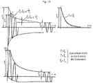
- a generator with 3.8 kVA power is loaded with nominal current using ohmic high-performance resistors.
- an all-phase short-circuit is brought about and the current curves which occur are recorded by means of an LEM converter and represented by a digital storage oscilloscope of the Tektronix TDS2002B type (cf. Fig. 3).
- Fig. 4 shows an example of a recorded and evaluated oscillogram. The curves shown represent the highest short-circuit current I k determined in several runs. The peak that occurred never exceeded the read and marked value of 8 • I nominal . This ratio of I k / I nominal is therefore used as the maximum value for all further subsequent exemplary calculations.
- the person skilled in the art can use the data sheets available for all commercially available semiconductor components (for example IGBTs or MOSFETs) to select suitable semiconductor components which can be used to carry out the method according to the invention or to build the device according to the invention. Analogously to the semiconductor switching elements in a corresponding form, this also applies to the other semiconductor components and other electronic components to be used for the device in the various embodiments.
- semiconductor components for example IGBTs or MOSFETs
- the semiconductor switching elements are used in the non-clocked pass mode.
- the following key data are relevant, for example, although this list is not to be understood as restrictive: - V CES [V] maximum permissible collector-emitter voltage - I C [A] maximum permissible collector continuous current - I CRM [A] maximum permissible, temporary collector current - T vjmax [° C] maximum permissible semiconductor core temperature - V CE (sat) max [V] Collector-emitter voltage drop with full control - R th (jc) [° C / (kW)] Heat transfer resistance semiconductor core - IGBT housing - R th (ch) [° C / (kW)] Heat transfer resistance IGBT housing - heat sink
- IGBTs semiconductor switching elements
- Table 1 Two commercially available semiconductor switching elements (IGBTs) with their corresponding characteristic data, which can be used for the method and the device according to the invention, are mentioned as examples in Table 1.
- the aforementioned selection criteria for the power semiconductors apply analogously and by way of example also to the configuration of the object of the invention as a semiconductor current limiting device.
- Table 1 Semiconductor switching elements that can be used as examples according to the invention
- R th (jc) 0.11 ° C / W 0.067 ° C / W *) each at 80 ° C
- Table 2 Exemplary operating temperatures Operating status Semicron Fujielectric 20 kVA P nominal (normal operation) 98.64 ° C 123.77 ° C 20 kVA after shutdown (3x I nominal for 1 ms) 100.76 ° C 125.64 ° C 20 kVA "worst case” (8x I nominal for 9 ms) 118.44 ° C 142.94 ° C
- the Fujielectric® IGBT can be used without departing from the scope of the invention or its equivalents, but because of the high operating temperatures this is less advantageous than using the Semikron® IGBT's.
- the low thermal resistance of the Fuji-IGBT is also not sufficient to remove the heat generated in the component quickly enough. In the worst case, exceeding the maximum permissible junction temperature T vjmax - which is 150 ° C for this type - cannot be excluded with sufficient certainty. If this temperature is exceeded, the thermal destruction of the IGBT or at least its damage is inevitable.
- At least one coil ie an “inductor”
- a processor or an FPGA or a corresponding analog control which triggers the current limitation, ie the supply of the defined surge short-circuit current is accomplished.
- at least one switch of classic design can also be provided.
- the network monitoring methods usually known from the prior art, i.e.
- the detection of error situations / operating faults which can be used according to the invention in order subsequently to carry out switching / control / regulation processes according to the invention are known to the person skilled in the art, for example from the corresponding standard regulations.
- the trigger threshold to be selected, or the trigger range, must be flexibly determined based on two objectives.
- short, uncritical load peaks such as those that occur when switching on or at the start of feed-in, must not lead to switch-off.
- the maximum current actually flowing in the event of a fault that is to say when a surge short-circuit current occurs, is to be limited to a minimum.
- the compromise chosen here as an example for trigger values lies in the range between two and a half to three times the nominal generator current.
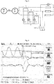
- the in Fig. 5 The measurement setup shown shows an example of a basic measurement setup for real-time current value acquisition.
- Other devices are known to the person skilled in the art and methods for current monitoring are known that can be used without departing from the scope of the invention or its equivalents.
- the flowing outer conductor currents ie the phase currents in phases L1, L2 and L3, are detected on the primary side by means of current transformers (for example current measuring transformers) T1, T2 and T3.
- current transformers for example current measuring transformers
- T1 T2 and T3 current measuring transformers
- Suitable electronic circuit arrangements for this purpose are known to the person skilled in the art and can be used according to the invention.
- the converters are short-circuited via three identical resistors (R mess ), which in turn are connected to each other in a star.
- R mess resistors
- the use of so-called "star circuits" and their advantageous use are known to the person skilled in the art.
- the flowing primary transformer current causes a secondary transformer current which has a fixed transmission ratio to the primary current and flows through the measuring resistors.
- the voltage drops occurring here at the resistors are recorded and fed to an evaluation circuit, which is shown in FIG Fig. 5 is not shown.
- Numerous evaluation circuits or measuring devices are known to the person skilled in the art from the prior art, which can be used without leaving the scope of the invention or its equivalents.
- the measuring resistors used should have the same values, if possible, in order to avoid measuring value falsifications between the individual outer conductors. If the measuring resistances have different values, this can be taken into account by means of appropriate correction factors and, if necessary, calibrations.
- the values of the resulting measuring voltages are directly proportional to the selected resistance values and can be calculated using Ohm's law.
- a voltage called "threshold voltage” drops in the order of magnitude of 0.6 to 0.7 V.
- This threshold voltage must be significantly exceeded by the measured values during nominal system operation in order to ensure the faultless switching function. If relatively small resistance values R mess of the order of a few milliohms are used, then the measured values U mess to be evaluated have relatively low voltage levels, which complicates the evaluation. This inevitably leads to further problems, since full rectification - especially in the voltage range from 0 to 0.7 V - is not guaranteed.
- the use of commercially available silicon diodes would therefore necessitate adjustments to the entire circuit in order to ensure reliable current measurement. It is therefore readily apparent to the person skilled in the art that the use of commercially available standard diodes falls within the scope of the invention and its equivalents, but is not a preferred embodiment.
- the three recorded measured values U mess-L1 , U mess-L2 and U mess-L3 are rectified using "active rectifiers".
- the core of these active rectifiers is formed by OPVs (so-called “operational amplifiers”) which have no threshold voltages. In this way, full rectification from 0 V is possible.
- Another advantage of this variant is the flexibility gained: On the one hand, the rectified measurement values can be raised or lowered to any voltage level within the OPV operating voltage ranges. On the other hand, in the measurement value acquisition - in direct comparison to the implementation with silicon diodes - no power is withdrawn, since OPVs are active components with a separate power supply. This minimizes falsifications of measurements.
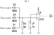
- Fig. 6 The preferred active rectification along with input and output variables of U mess-L1 is shown as an example (circuit diagram in the upper half, storage oscilloscope image in the lower half).
- a 50 Hz sine with an amplitude of 1 V peak was chosen as an exemplary input variable.
- auxiliary line drawn horizontal line at 0.0 V
- rectification is already proven from 0 V, completely without any threshold voltage occurring.
- the increased voltage level of the output variable compared to the input variable can also be seen.
- the use of exactly identical rectifiers for the individual measuring voltages U mess-L1 , U mess-L2 and U mess-L3 is particularly preferred.
- further embodiments falling within the scope of the invention and its equivalents also have different rectifiers and thus make it possible to monitor the individual phases independently of one another with different sensitivity.
- the rectified measured values obtained as described above, preferably identically, are as in Fig. 7 described merged and decoupled from each other by means of diodes.
- the sum signal U mess-sum thus obtained which shows the voltage curve analogous to the output voltage of a B6 bridge circuit has, as is generally known to the person skilled in the art, a comparator (for example component "LT1721" in Fig. 7 ) fed.
- a comparator compares two input variables and makes a digital case distinction. If the input voltage is less than the comparison variable ( Fig. 7 : 1.5 V reference voltage source V7), the output level corresponds to almost 0 V. If the input voltage exceeds the reference voltage, the output level takes on the operating or supply voltage level of the comparator.
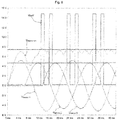
- Fig. 8 illustrates how it works using the exemplary simulation of an overload of L1.
- the voltage curves of U mess-L1 , U mess-L2 and U mess-L3 are shown , the rectified sum signal U mess-sum at the comparator input and the voltage curve at the comparator output (V [out]).
- the reference voltage used on the comparator is 7.5 V. It can be clearly seen that U mess-L1 has the highest amplitude due to the overload. After rectification and signal merging, there are slight overshoots in which the reference voltage is exceeded at certain points. Every time the comparator is exceeded, the "V (out)" curve takes on Fig.
- the switch-off device must either store a recognized network fault (i.e. a surge short-circuit current that has led to the switch-off) and remain switched off in order to then be switched on again by a higher-level network controller; in this case, the device must have at least one 1-bit error memory, which is reset when it is switched on again by the higher-level network controller.
- the method according to the invention or the device according to the invention comprises a control step or an internal control module (synonymously control) and has hardware and / or software implemented connection conditions when the method or the device itself fulfills the re-connection of the synchronous generator can make / cause
- an error memory is preferably used, which comprises at least 2 bit storage capacity.
- IGBTs are used as switches and "controlled” in order to implement the switching state "ON".
- the person skilled in the art knows how to control IGBTs or other non-mechanical switching elements so that current can flow.
- the collector-emitter path becomes conductive, the collector potential here having to be higher than that of the emitter.
- the currents to be switched are AC currents, the use of two IGBTs per outer conductor is essential. Both emitter connections are interconnected (anti-parallel Arrangement / connection) and due to the usually internally installed free-wheeling diode, the current paths result completely automatically.
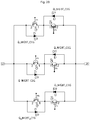
- Fig. 9 shows an example of a corresponding circuit diagram. Is that in Fig.
- varistors are provided parallel to the collector-emitter path of each IGBT (cf. Fig. 9 ).
- V CES maximum permissible collector-emitter voltage
- the varistor used should correspond approximately to this value.
- a usable type would be, for example, the Z80M112 from the manufacturer CKE®. The nominal breakdown voltage of this type is 1100 V ⁇ 10%. So the maximum voltage before the breakdown is 1210 V.
- the experimental data (e.g. currents, voltages, times, switching states) were recorded in all experiments / examples using a storage oscilloscope.
- the configuration of the object of the invention as a device for ensuring network stability in power supply networks by limiting a surge short-circuit current provides the following configuration options, which are described below by way of example with reference to the figures 11A-C are described in more detail.
- connection pins of the components can be selected at least in part, so that the numbers generated by the software of Connection pins of the same pins (eg emitter, collector, gate for transistors) can have different numbers in different drawings.
- the same reference symbols in different drawings in each case in connection with curved arrows always denote the same technical feature.
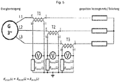
- Figure 11A shows the example of a three-phase power network, a first exemplary embodiment of the object of the invention for feeding a defined short-circuit current into a power network (phases L1 to L3, with the addition "ext" each identifying the external network side, ie the higher-level power network into which is fed ).
- the reference numerals 10 and 10 ' each denote the two semiconductor switching elements which are connected antiparallel to one another in one phase of the power network, in the present example with an integrated free-wheeling diode (not shown).
- This exemplary embodiment also has a varistor ( 20 ) connected in parallel with the respective semiconductor switching elements in each phase, as well as the additional inductance (coil) with the reference symbol 30 , which in this simplest embodiment variant already enables surge short-circuit currents to be limited and / or to be built up in a controlled manner.
- the processor or FPGA which is also required, or the corresponding analog control for triggering the current limitation, ie the supply of the defined surge short-circuit current, is not shown; the control signal lines required for this are connected to the connections of the semiconductor switching elements marked here with “2”.
- the principle of operation is such that the structure of the magnetic field in the inductance (coil 30 ) in the phase line creates a “buffer store” for the current fed in, from which, when disconnected from the mains, ie when the semiconductor switching elements 10, 10 'are opened, and the resulting breakdown of the magnetic field, the energy "flowing" out of the collapsing magnetic field is fed into the power network as a defined short-circuit current with decreasing intensity becomes.
- Corresponding software algorithms or analog control circuits with which this can be achieved according to the invention are known to the person skilled in the art and for the sake of clarity in the Figure 11A , 11B and 11C Not shown.
- Figure 11B also shows, using the example of a three-phase power network, a second exemplary embodiment of the object of the invention for feeding a defined short-circuit current into a power network (phases L1 to L3, the addition "ext” also feeding the external network side, ie the superordinate power network, into the here is marked).
- the reference numerals 10 and 10 ' here also denote the two semiconductor switching elements which are connected antiparallel to one another in a phase of the power network, in the present example also with an integrated free-wheeling diode (not shown).
- This exemplary embodiment also has the additional inductance (coil) 30 , which makes it possible to limit surge short-circuit currents and / or to build them up in a controlled manner, but does not require any varistors connected in parallel in the phases to the respective semiconductor switching elements 10, 10 ' , because the excess current is at this Embodiment not caught by consumers (eg varistors), but by means of appropriate control of the additional paired anti-parallel semiconductor switching elements 40, 40 ' in each of the two other phases, which still has capacity for the current flow.
- inductance (coil) 30 which makes it possible to limit surge short-circuit currents and / or to build them up in a controlled manner, but does not require any varistors connected in parallel in the phases to the respective semiconductor switching elements 10, 10 ' , because the excess current is at this Embodiment not caught by consumers (eg varistors), but by means of appropriate control of the additional paired anti-parallel semiconductor switching elements 40, 40 ' in each of the two other phases, which still has
- the necessary control of the semiconductor switching elements 40, 40 ' connected between the phases is also carried out according to the invention in a manner known from the prior art by means of a processor or FPGA or a corresponding analog control, the signal lines here also being connected to the connections marked "2" Semiconductor switching elements are connected.
- the processor or FPGA which is also required, or the corresponding analog control for triggering the current limitation, as well the redirection of the surge short-circuit current into another phase, ie the supply of the defined surge short-circuit current not shown.
- Figure 11C also shows, using the example of a three-phase power network, a third exemplary embodiment of the object of the invention for feeding a defined short-circuit current into a power network (phases L1 to L3, the addition "ext” here also feeding the external network side, ie the higher-level power network, into the is marked).
- the reference numerals 10 and 10 ' here also denote the two semiconductor switching elements which are connected antiparallel to one another in a phase of the power network, in the present example also with an integrated free-wheeling diode (not shown).
- This exemplary embodiment also has the additional inductance (coil) 30 , which makes it possible to limit surge short-circuit currents and / or to build them up in a controlled manner, but does not require any varistors connected in parallel in the phases to the respective semiconductor switching elements 10 , 10 ' , because the excess current is at this Embodiment not caught by consumers (eg varistors), but redirected by means of appropriate control of the additional pairs of anti-parallel semiconductor switching elements 40, 40 ' in the neutral conductor ("N”), which naturally still has capacity for the current flow.
- inductance (coil) 30 which makes it possible to limit surge short-circuit currents and / or to build them up in a controlled manner, but does not require any varistors connected in parallel in the phases to the respective semiconductor switching elements 10 , 10 ' , because the excess current is at this Embodiment not caught by consumers (eg varistors), but redirected by means of appropriate control of the additional pairs of anti-parallel semiconductor switching elements 40, 40
- the required control of the semiconductor switching elements 40, 40 ' connected between the phases and the neutral conductor is likewise carried out according to the invention in a manner known from the prior art by means of a processor or FPGA or a corresponding analog control, the signal lines here also being connected to the "2" marked connections of the semiconductor switching elements are connected.
- the processor or FPGA or the corresponding analog control for triggering the current limitation and the redirection of the surge short-circuit current into the neutral conductor is also not shown.
Abstract
Gegenstand der Erfindung sind ein Verfahren zur Kontrolle (d.h. Verhinderung oder Reduzierung) von Stoßkurzschlußströmen in Stromverteilungsnetzen beim Zubau von Asynchron- oder Synchrongeneratoren, bzw. bei der Anbindung von untergeordneten Teilnetzen an übergeordnete Stromverteilungsnetze, sowie die Vorrichtung dazu und deren Verwendung. Bevorzugter Einsatzbereich sind Niederspannungsnetze, die an eng vermaschte Mittelspannungsnetze zwischen 1 kV und 50 kV angebunden sind.The invention relates to a method for the control (i.e. prevention or reduction) of surge short-circuit currents in power distribution networks when adding asynchronous or synchronous generators, or in the connection of subordinate subnetworks to higher-level power distribution networks, and the device therefor and their use. Preferred areas of application are low-voltage networks that are connected to tightly meshed medium-voltage networks between 1 kV and 50 kV.
Description
Die vorliegende Erfindung betrifft ein Verfahren zur Kontrolle von Stoßkurzschlußströmen, d.h. der Einstellung auf einen bestimmten Wert oder eine komplexe Situation durch Begrenzung und/oder kontrollierten Aufbau der Stoßkurzschlußsttöme in Stromverteilungsnetzen sowie die Vorrichtung dazu ("Halbleiter-Steuervorrichtung", bzw. synonym "Halbleiter-Kontrollvorrichtung") und deren Verwendung.The present invention relates to a method for controlling surge short-circuit currents, i.e. the setting to a certain value or a complex situation by limiting and / or controlled construction of the surge short-circuit currents in power distribution networks and the device therefor (“semiconductor control device” or synonymously “semiconductor control device”) and their use.
Die erfindungsgemäße Vorrichtung und das erfindungsgemäße Verfahren dienen somit zur Sicherstellung der Netzstabilität in Stromversorgungsnetzen, bevorzugt in solchen mit kleinräumig verteilten Einspeisepunkten, was üblicherweise bei Mittelspannungsnetzen der Fall ist.The device according to the invention and the method according to the invention thus serve to ensure the grid stability in power supply networks, preferably in those with small-area distributed feed-in points, which is usually the case with medium-voltage networks.
Die vorliegende Erfindung betrifft ein Verfahren zur Unterdrückung (d.h. Verhinderung oder Reduzierung) von Stoßkurzschlußströmen in Stromverteilungsnetzen sowie die Vorrichtung dazu ("Halbleiter-Abschaltvorrichtung") und deren Verwendung. Weiterhin betrifft die vorliegende Erfindung auch eine Vorrichtung und ein Verfahren zur Erzeugung und Einspeisung definierter Kurzschlußströme in das Stromnetz, so daß dieses dadurch hochgefahren/gestartet, d.h. in Betrieb genommen oder in Betrieb gehalten werden kann, obwohl es sich in einem instabilen Betriebszustand befindet ("Halbleiter-Strombegrenzungsvorrichtung"). Beide Teilaspekte der vorliegenden Erfindung (Halbleiter-Strombegrenzungsvorrichtung und Halbleiter-Abschaltvorrichtung, bzw. jeweils Verfahren) dienen jeder für sich alleine oder in Kombination miteinander der Sicherstellung der Netzstabilität.The present invention relates to a method for suppressing (ie preventing or reducing) surge short-circuit currents in power distribution networks and to the device therefor (“semiconductor shutdown device”) and the use thereof. Furthermore, the present invention also relates to a device and a method for generating and feeding defined short-circuit currents into the power grid, so that it can be started up, ie started up or kept in operation, even though it is in an unstable operating state (" Semiconductor current limiting device "). Both partial aspects of the present invention (semiconductor current limiting device and semiconductor switch-off device, or respectively methods) each serve to ensure the stability of the network on their own or in combination with one another.
Mit zunehmender Zuschaltung von lokalen (also dezentralen) Stromerzeugern an die Stromverteilungsnetze wächst die Notwendigkeit, den Beitrag dieser zugebauten Anlagen an Stoßkurzschlußströmen im Stromverteilungsnetz zu unterdrücken. In manchen Fällen ist aber eine komplexere Reaktion als eine einfache Abschaltung notwendig. Daher ist es vorteilhaft für die Netzstabilität, wenn ein in einen instabilen Betriebszustand geratenes Stromnetz durch Einspeisung definierter Kurzschlußströme von den Einspeisepunkten der dezentralen Stromerzeuger aus (bzw. von untergeordneten Teilnetzen aus, d. h. "von unten") hochgefahren (gestartet, in Betrieb genommen) oder bei lediglich eingetretener Instabilität wieder stabilisiert werden kann. Letzteres entspricht der Situation, daß das untergeordnete Teilnetz bzw. der (Netz-)Einspeisepunkt während einer Instabilität (Netzinstabilität) weiterhin in Betrieb gehalten wird.With the increasing connection of local (i.e. decentralized) power generators to the power distribution networks, the need to suppress the contribution of these additional installations to surge short-circuit currents in the power distribution network increases. In some cases, however, a more complex reaction than a simple shutdown is necessary. It is therefore advantageous for the stability of the grid if a power grid that has become unstable by starting up defined short-circuit currents from the feed-in points of the decentralized power generators (or from subordinate subnets, ie "from below") is started up (started, put into operation) or can be stabilized again only if instability has occurred. The latter corresponds to the situation in which the subordinate subnet or the (network) entry point continues to be operated during an instability (network instability).
Die Definition, was unter einer (Netz-)Instabilität sowie deren Erkennung und Beseitigung zu verstehen ist, ist in entsprechenden Normvorgaben geregelt und dem Fachmann bekannt. Daraus ergeben sich auch in bekannter Weise die zu erfassenden Grenzwerte an Strömen und Spannungen, um einen Netzfehler als solchen zu erkennen sowie Vorgaben zu seiner Beseitigung. Beispiele für derartige Regelungen sind die DIN EN 60909-0:2013-02 und die VDE 0102:2013-02, worin die Berechnung und implizit auch die Erfassung der Kurzschlusströme geregelt sind. Grundsätzlich gibt der Netzbetreiber einen zulässigen Kurzschlusstrom für die Anlage vor - ist dieser Strom überschritten, muss die Anlage den Strom begrenzen oder abschalten. Die VDE-AR-N 4105 gibt im Bereich der Niederspannung, und die VDE-AR-N 4110 im Bereich der Mittelspannung Fehler vor, bei denen die Anlage dennoch für bestimmte Zeiten am Netz bleiben muss.The definition of what is to be understood as (network) instability as well as its detection and elimination is regulated in corresponding standard specifications and is known to the person skilled in the art. This also results in the known limit values for currents and voltages, in order to recognize a network fault as such, as well as guidelines for its elimination. Examples of such regulations are DIN EN 60909-0: 2013-02 and VDE 0102: 2013-02, which regulate the calculation and implicitly the detection of short-circuit currents. Basically, the network operator specifies a permissible short-circuit current for the system - if this current is exceeded, the system must limit or switch off the current. The VDE-AR-N 4105 specifies errors in the area of low voltage and the VDE-AR-N 4110 in the area of medium voltage, for which the system must nevertheless remain connected to the network for certain times.
Besonders in dicht ausgebauten Mittelspannungsnetzen, d.h. Stromverteilungsnetzen, die im Bereich von 1 kV bis 50 kV betrieben werden, ist der zusätzliche Anschluß von Asynchron- und besonders von Synchrongeneratoren zur Stromerzeugung problematisch, da diese einen hohen Stoßkurzschlußstrom aufweisen. Dies gilt analog auch auf übergeordneter Ebene für Stromverteilungsnetze, die mit derartigen Mittelspannungsnetzen verbunden sind, aus denen - bedingt durch die hoch variable Einspeisungsleitung dezentraler regenerativer Stromerzeuger - Stoßströme in das übergeordnete Stromnetz resultieren können. Ein Generator vom Typ Leroy-Somer LSA 43.2, der typisch ist für kleine Blockheizkraftwerke ("BHKW"), hat bei einem Nennstrom von 115 A einen maximalen Stroßstrom von ca. 1 kA (vgl.
Zur Lösung derartiger Probleme gibt es im Stand der Technik folgende Möglichkeiten:
- Mechanische Schalter - diese haben ein hohes Isolationsvermögen, weisen niedrige Verluste auf und sind wieder einschaltbar. Sie sind jedoch für diesen Zweck, die Vermeidung von Stoßströmen in Stromverteilungsnetzen, zu langsam.
- Sicherungen - diese sind jedoch nicht wieder einschaltbar und ebenfalls zu langsam.
- Is-Begrenzer (oder Is-Schaltungen) - bei diesen Vorrichtungen wird eine Sprengkapsel ausgelöst, die die Erzeugungseinrichtung schnell vom Netz trennt. Über komplexe Ansteuerungen sind diese Vorrichtungen selektiv genug, um für den Zweck eingesetzt werden zu können, aber sehr teuer (> 70000 €) und nicht wieder einschaltbar. Sie müssen daher nach einmaliger Auslösung ersetzt werden. Mit "selektiv" ist gemeint, dass über die komplexe Ansteuerung des Is-Begrenzers in Echtzeit erkannt werden muß, wann ein echter Stoßkurzschlußstrom vorliegt, und wann es sich im aktuellen Fall lediglich um eine weniger kritische Netzinstabilität (sog. "Flicker" aufgrund von an sich unkritischen mechanischen Schaltvorgängen) handelt. Nur im Falle eines echten Stoßkurzschlußstroms darf der Is-Begrenzer auslösen.
- Umrichter - diese weisen hohe Verluste auf und sind ebenfalls sehr teuer.
- Mechanical switches - these have a high insulation capacity, have low losses and can be switched on again. However, they are too slow for this purpose, the avoidance of surge currents in power distribution networks.
- Fuses - these cannot be switched on again and are also too slow.
- I s limiter (or I s circuits) - a detonator is triggered in these devices, which quickly disconnects the generating device from the network. Using complex controls, these devices are selective enough to be used for the purpose, but are very expensive (> € 70,000) and cannot be switched on again. They must therefore be replaced after a single trigger. By "selective" it is meant that the complex control of the I s limiter must be used to recognize in real time when there is a real surge short-circuit current and when in the current case it is merely a less critical network instability (so-called "flicker" due to mechanical switching processes that are not critical in themselves). The I s limiter may only trip in the event of a real surge short-circuit current.
- Inverters - these have high losses and are also very expensive.
Die hier offenbarte Halbleiter-Abschaltvorrichtung ermöglicht es, diesen Stoßkurzschlußstrom in einem Überschreitungsfall mehr oder weniger hart abzuschalten. Dies ist besonders günstig bei einem Anschluss in der Umgebung von schwach ausgebauten Mittelspannungsnetzen, die keinen weiteren Kurzschlussstrom aufnehmen können.The semiconductor switch-off device disclosed here makes it possible to switch off this surge short-circuit current more or less hard in the event of an overshoot. This is particularly advantageous for a connection in the vicinity of poorly developed medium-voltage networks that cannot take up any further short-circuit current.
Im Hinblick auf zukünftige Stromnetze, die im Wesentlichen aus dezentral verteilten erneuerbaren Stromerzeugern bestehen (mit begrenzter Fähigkeit, Kurzschlußstrom bereitzustellen), wird sich diese Möglichkeit als ungenügend herausstellen. Zum einen basiert der Distanzschutz auf definierten Überströmen und zum anderen wird die "low Voltage ride Through"-Fähigkeit für ein stabiles Netz ohne Großkraftwerke wichtiger. Unter "low Voltage ride Through" versteht der Fachmann die - zumindest teilweise - Toleranz von elektrischen Erzeugungseinheiten wie Generatoren (oder generell Einspeiseeinheiten wie etwa auch untergeordnete Teilnetze gegenüber dem jeweils übergeordneten Netz) gegenüber kurzzeitigen Spannungseinbrüchen: Eine Erzeugungs-/Einspeiseeinheit darf sich bei Spannungseinbrüchen nicht unmittelbar vom Stromnetz trennen, sondern muss eine bestimmte Zeit weiter mit dem Netz verbunden bleiben und zumindest teilweise weiterhin Strom einspeisen. Kurzzeitige Spannungseinbrüche können zum Beispiel infolge von Netzfehlern wie etwa bei Kurzschlüssen, Erdschlüssen oder Blitzeinschlägen auftreten. Durch die Fähigkeit von dezentralen Erzeugungsanlagen bzw. untergeordneten Teilnetzen zum "low Voltage ride Through" wird ein großflächiger Netzzusammenbruch infolge eines Dominoeffektes von vielen kleineren Erzeugungeranlagen/Teilnetzen bei Fehlern im übergeordneten Übertragungsnetz verhindert. Verfahren und Vorrichtungen zur Sicherstellung des Distanzschutzes sind dem Fachmann aus dem Stand der Technik ebenfalls bekannt, beispielsweise in Form von Distanzschutzrelais. Insbesondere in der Übergangsphase des Netzumbaus ist die Fähigkeit, den Überstrom kontrolliert an das Netz abzugeben von großem Nutzen. Dies gilt ganz besonders ab dem Zeitpunkt, ab dem die Großkraftwerke nicht mehr genug Strom zur Verfügung stellen können, um die Netzstabilität überwiegend sicherzustelllen. In einem von Grund auf vollständig neu dezentral konzipierten Netz könnte man das gesamte Sicherheitskonzept neu aufstellen, in bereits bestehenden ("historisch gewachsenen") Netzen besteht diese Möglichkeit der vollständigen Neukonzeption der Netzsicherheit nicht. Die vorliegende Erfindung befasst sich daher auch mit der kontrollierten Bereitstellung von variabel einstellbaren Kurzschlußströmen in ein Nieder- oder Mittelspannungsnetz.With regard to future electricity grids, which essentially consist of decentrally distributed renewable electricity generators (with limited ability to provide short-circuit electricity), this possibility will prove to be insufficient. On the one hand, distance protection is based on defined overcurrents and, on the other hand, the "low voltage ride through" capability is more important for a stable network without large power plants. "Low voltage ride through" is understood by the person skilled in the art to mean the - at least partially - tolerance of electrical generation units such as generators (or generally supply units such as also subordinate subnetworks to the respective higher-level network) with respect to short-term voltage dips: A generation / supply unit must not be in the event of voltage dips disconnect directly from the power grid, but must remain connected to the grid for a certain period of time and at least partially continue to feed in electricity. Brief voltage drops can occur, for example, as a result of network faults such as short circuits, earth faults or lightning strikes. The ability of decentralized generation systems or subordinate subnets to "low voltage ride through" prevents a large-scale network breakdown due to a domino effect of many smaller generator systems / subnetworks in the event of errors in the higher-level transmission network. Methods and devices for ensuring distance protection are also known to the person skilled in the art from the prior art, for example in the form of distance protection relays. The ability to deliver the overcurrent to the grid in a controlled manner is particularly useful in the transition phase of the grid conversion. This is especially true from the point at which large power plants can no longer provide enough electricity, to ensure network stability for the most part. In a completely new, decentralized network, the entire security concept could be reorganized; in existing ("historically grown") networks, there is no possibility of a completely new conception of network security. The present invention therefore also deals with the controlled provision of variably adjustable short-circuit currents in a low or medium voltage network.
Bezüglich des Wieder-Hochfahrens, d.h. des Starts von Stromnetzen gibt es im Stand der Technik keinerlei Möglichkeit, dies "von unten", d.h. ausgehend von einzelnen Netzeinspeiseknoten oder von Umrichterstationen vom untergeordneten Netz (bzw. der Einspeisevorrichtung) heraus vorzunehmen. (Bei einem Einspeisepunkt handelt es sich letztendlich ebenfalls um einen Netzknoten, und zwar um einen solchen, der sich am Rande des Netzes befindet, also "randständig" ist.) Im Stand der Technik kann ein ausgefallenes (Teil-)Stromnetz nur von der übergeordneten Instanz (d.h. dem übergeordneten Netz) aus wieder in Betrieb genommen werden. Dies ist nachteilig für eine schnelle (ggf. automatisierte) Wiederinbetriebnahme nach Netzausfall, da eine übergeordnete Instanz zur Steuerung des Hochfahr-Prozesses zwingend erforderlich ist, die zunächst alle "Bereitschaftsmeldungen" der untergeordneten Netze entgegennehmen und bewerten muß, um diese untergeordneten Netze dann anschließend nach und nach wieder an das übergeordnete Netz anzuschließen.Regarding the restart, i.e. the start of power grids there is no way in the prior art to do this "from below", i.e. starting from individual network feed-in nodes or converter stations from the subordinate network (or the feed-in device). (In the end, an entry point is also a network node, namely one that is located on the edge of the network, that is to say "on the edge.") In the prior art, a failed (partial) power network can only be accessed by the parent Instance (ie the higher-level network) can be put into operation again. This is disadvantageous for a quick (possibly automated) recommissioning after a power failure, since a higher-level authority for controlling the start-up process is absolutely necessary, which must first receive and evaluate all "ready messages" from the lower-level networks, and then subsequently to these lower-level networks and then reconnect to the higher-level network.
Aufgabe der vorliegenden Erfindung ist es, die im Stand der Technik bestehenden Probleme zu lösen, indem ein Verfahren und eine Vorrichtung bereitgestellt wird, um Stoßströme ausreichend schnell sicher zu erkennen und zu begrenzen, und dadurch Stromverteilungsnetze vor Stoßströmen zu schützen. Das Verfahren bzw. die Vorrichtung soll zudem kostengünstig und wiederverwendbar, d.h. wiedereinschaltbar sein, so dass keine Unterscheidung zwischen echten Stoßkurzschlußströmen und lediglich unkritischen Netzinstabilitäten infolge harmloser mechanischer Schaltvorgänge ("Flicker") getroffen werden muß.The object of the present invention is to solve the problems existing in the prior art by providing a method and a device for reliably detecting and limiting surge currents sufficiently quickly and thereby protecting power distribution networks from surge currents. The method and the device should also be inexpensive and reusable, that is to say that they can be switched on again, so that no distinction is made between real surge short-circuit currents and only uncritical network instabilities due to harmless mechanical switching processes ("flicker") must be taken.
Aufgabe der vorliegenden Erfindung ist es weiterhin, nicht nur die im Stand der Technik bestehenden Probleme bezüglich Vermeidung von Stoßkurzschlußströmen zu lösen (wie vorstehend beschrieben), sondern ebenfalls, eine Möglichkeit bereitzustellen, übergeordnete, in kritischem Betriebszustand befindliche oder ausgeschaltete, Stromnetze aus untergeordneten Stromnetzen heraus wieder hochzufahren, d.h. zu starten/in Betrieb zu nehmen bzw. zu stabilisieren, indem ein Verfahren und eine Vorrichtung bereitgestellt wird, womit durch Einspeisung definierter Kurzschlußströme aus dem untergeordneten Netz in das übergeordnete Netz und Beobachtung des Verhaltens des übergeordneten Netzes, das übergeordnete Netz aus dem untergeordneten heraus in Betrieb genommen bzw. stabilisiert werden kann. Welche für die Beobachtung des Verhaltens des übergeordneten Netzes erforderlichen Netzparameter (wie beispielsweise Spannung, Stromfluß, Phasenlage und dergleichen) zu überwachen sind, sowie die Art der Bestimmung der erforderlichen Parameter, ist dem Fachmann aus dem Stand der Technik sowie aus den einschlägigen Normvorgaben bekannt.Another object of the present invention is not only to solve the problems in the prior art relating to the prevention of surge short-circuit currents (as described above), but also to provide a possibility for superordinate, critical operating or switched off power networks from subordinate power networks to start up again, ie to start / put into operation or to stabilize by providing a method and a device with which by feeding defined short-circuit currents from the lower-level network into the higher-level network and observing the behavior of the higher-level network, the higher-level network from within the lower level Can be put into operation or stabilized. The person skilled in the art is familiar with the state of the art and the relevant standard specifications as to which system parameters (such as voltage, current flow, phase position and the like) to be monitored for monitoring the behavior of the higher-level network are to be monitored.
Die Gesamtaufgabe besteht somit darin, Stoßkurzschlußströme in Stromnetzen zu kontrollieren, d.h. abzuschalten oder auf einen definierten Kurzschlußstrom zu begrenzen, und setzt sich aus den beiden Teilaufgaben "Stoßkurzschlußströme abschalten" und "Kurzschlußströme begrenzen/definiert erzeugen" zusammen, wobei jede der beiden Teilaufgaben für sich bereits eine erfindungsgemäße Kontrolle von Stoßkurzschlußströmen darstellt, und somit eine technische Verbesserung der Netzstabilität bewirkt.The overall task is to control surge short-circuit currents in power grids, i.e. switch off or limit to a defined short-circuit current, and is made up of the two subtasks "switch off surge short-circuit currents" and "limit short-circuit currents / generate defined", each of the two sub-tasks already represents an inventive control of surge short-circuit currents, and thus a technical improvement network stability.
Diese Aufgabe wird erfindungsgemäß gelöst durch die kennzeichnenden Merkmale des Hauptanspruchs 1 sowie der nebengeordneten Verfahrens- sowie Verwendungsansprüche 6, 14, 15, 17 und 18. Die Unteransprüche stellen vorteilhafte Ausgestaltungen der Erfindung dar. Im Zuge der Beschreibung der Erfindung sowie der Ansprüche gemachte Bereichsangaben umfassen stets alle - nicht genannten - Zwischenwerte und alle denkbaren Teilintervalle.This object is achieved according to the invention by the characterizing features of
Die Erfordernis der Selektivität, wie sie für Is-Begrenzer zwingend erforderlich ist, besteht bei dem erfindungsgemäßen Verfahren und der erfindungsgemäßen Vorrichtung nicht, denn infolge der Reversibilität des Schaltvorganges kann der über die erfindungsgemäße Abschaltvorrichtung an das Spannungsnetz angeschlossene Asynchron- oder Synchrongenerator günstigenfalls bereits in der nächsten Halbwelle wieder zugeschaltet werden, und zwar entweder durch die übergeordnete Netzsteuerung oder ggf. durch die in der Erfindung enthaltene interne Eigensteuerung.The requirement of selectivity, as is absolutely necessary for I s limiters, does not exist in the method and the device according to the invention, because, due to the reversibility of the switching process, the asynchronous or synchronous generator connected to the voltage network via the switch-off device according to the invention can, in a favorable manner, already be in the next half-wave are switched on again, either by the higher-level network control or, if necessary, by the internal self-control contained in the invention.
Die erfindungsgemäße Lösung zur Erreichung der erforderlichen hohen Schaltgeschwindigkeiten basiert bevorzugt auf Halbleitern; sie weist zwar natürlicherweise auch Verluste auf, ähnlich wie die im Stand der Technik bekannten Standardlösungen, dies ist jedoch insgesamt nicht nachteilig, da die mehrfache Reversibilität des Schaltvorganges dazu führt, dass die erfindungsgemäße Vorrichtung, d.h. der Schalter, verschleißfrei arbeitet. Als "Schalter" wird hier und im Folgenden die gesamte erfindungsgemäße Abschaltvorrichtung (Synonym: "Halbleiter-Abschaltvorrichtung") bezeichnet; das eigentliche schaltende Halbleiterbauteil, beispielsweise ein IGBT oder ein MOSFET ( m etal- o xide- s emiconductor f ield e ffect t ransistor), wird zur Unterscheidung davon als "Halbleiterschaltelement" bezeichnet und die antiparallele Anordnung zweier derartiger Halbleiterschaltelemente als "bidirektionaler Halbleiterschalter". Die schaltenden Halbleiterbauteile sind diejenigen Bauteile der Vorrichtung, die die Fähigkeit aufweisen, Ströme abzuschalten.The solution according to the invention for achieving the required high switching speeds is preferably based on semiconductors; although it naturally also has losses, similar to the standard solutions known in the prior art, this is not disadvantageous overall, since the multiple reversibility of the switching process means that the device according to the invention, ie the switch, operates without wear. The “switch” here and in the following refers to the entire shutdown device according to the invention (synonym: “semiconductor shutdown device”); the actual switching semiconductor component, such as an IGBT or a MOSFET (m etal- o xide- s emiconductor F ield e ffect t Transistor) is referred to and to distinguish them as "semiconductor switching element" the anti-parallel arrangement of two such semiconductor switching elements as a "bi-directional semiconductor switch". The switching semiconductor components are those components of the device that have the ability to switch off currents.
Die erfindungsgemäße Ausgestaltung der Vorrichtung mit mindestens einem induktiven Element (z. B. einer Spule) mit definierter Induktivität zur Erzeugung und Einspeisung definierter Kurzschlußströme in das Stromnetz wird im Rahmen dieser Offenbarung als "Strombegrenzer" bezeichnet, da durch sie bewirkt wird, daß die Netzstabilität erhöht wird durch Begrenzen und Einspeisen des Stoßkurzschlußstromes aus dem untergeordneten Netz bzw. aus dem Einspeisepunkt in das übergeordnete Netz. Dies entspricht auch dem Verbinden eines in Betrieb befindlichen BHKW's oder eines in Betrieb befindlichen Teilnetzes mit einem nicht in stabilem Betriebszustand befindlichen übergeordneten Netz. Das heißt, die gesamte erfindungsgemäße Vorrichtung zur Kontrolle von Stoßkurzschlußströmen umfasst zwei grundsätzliche Ausführungsvarianten:
- a) die gesamte erfindungsgemäße Abschaltvorrichtung (Synonym: "Halbleiter-Abschaltvorrichtung", auch "Schalter" oder "Halbleiter-Abschaltvorrichtung" genannt), und
- b) die gesamte erfindungsgemäße "Strombegrenzungsvorrichtung" (synonym "Strombegrenzer", oder auch "Halbleiter-Strombegrenzungsvorrichtung" genannt), die die Vorrichtung gemäß Absatz a) umfasst und darüber hinaus mindestens ein induktives Element (z.B. eine Spule) mit definierter Induktivität, mindestens einen Prozessor oder einen FPGA oder eine entsprechende dem Fachmann bekannte analoge Steuerschaltung, sowie optional mindestens ein weiteres Halbleiterschaltelement aufweist.
- a) the entire shutdown device according to the invention (synonym: “semiconductor shutdown device”, also called “switch” or “semiconductor shutdown device”), and
- b) the entire "current limiting device" according to the invention (synonymously "current limiter", or also called "semiconductor current limiting device"), which comprises the device according to paragraph a) and moreover at least one inductive element (for example a coil) with a defined inductance, at least one Processor or an FPGA or a corresponding analog control circuit known to the person skilled in the art, and optionally has at least one further semiconductor switching element.
Diese beiden Teilaspekte können sowohl unabhängig voneinander realisiert, d.h. vorgesehen/verwendet werden, als auch in Kombination miteinander. Bei Realisierung in Kombination miteinander ist eine Steuerungs-/Regelungslogik vorzusehen, die erfindungsgemäß bevorzugt lokal implementiert oder per Fernwartung vorgesehen sein kann, und die je nach aktuellem Betriebszustand des Netzes den aktuellen Betriebszustand der Vorrichtung zur Kontrolle von Stoßkurzschlußströmen wie folgt einstellt: Ist das Netz stabil in Betrieb, wird in den Modus der Abschaltung von Stoßkurzschlußströmen geschaltet, ist das Netz außer Betrieb oder in einem kritischen Betriebszustand, wird in den Modus der definierten Erzeugung und Einspeisung von Kurzschlußströmen geschaltet.These two sub-aspects can be implemented independently of one another, ie provided / used, or in combination with one another. When implemented in combination with one another, control logic is to be provided, which according to the invention can preferably be implemented locally or provided by remote maintenance, and which, depending on the current operating state of the network, sets the current operating state of the device for controlling surge short-circuit currents as follows: Is the network stable in operation, is switched to the mode of switching off surge short-circuit currents, the network is out of operation or in a critical operating state, is switched to the mode of defined generation and supply of short-circuit currents.
Diese Aufgabe (die Einspeisung definierter Kurzschlußströme) wird durch eine Anordnung von bidirektionalen Schaltern und Induktivitäten gelöst, die - wenn sie hinter einen Synchron- oder Asynchrongenerator geschaltet sind - durch ihre Ansteuerung einen Kurzschlussstrom oder jeden anderen Strom auf einen gewünschten Wert einstellen und diesen Strom auch für eine vorgegebene Zeit halten können. Die maximal mögliche Zeit ergibt sich aus der Bauteilauswahl und kann gegebenenfalls auch unbegrenzt sein. Ausschlaggebend ist hierbei vor allem die bauartbedingt vorgegebene Verlustleistung der Bauteile, bzw. die Ausgestaltung der Kühlung der Vorrichtung. Ist diese so gestaltet, dass die maximale Bauteiltemperatur nicht überschritten wird, ist ein unbegrenzter Betrieb, d.h. die zeitlich unbegrenzte Aufrechterhaltung des Kurzschlußstromes, möglich. Dem Fachmann ist aus dem Stand der Technik bekannt, wie die Bauteile zu dimensionieren/auszuwählen sind, bzw. die Kühlung auszugestalten ist, um so einen bestimmten Zeitraum für die Aufrechterhaltung des einzuspeisenden Kurzschlußstromes vorzugeben, bzw. zeitlich unbegrenzte Einspeisung des definierten Kurzschlußstroms zu ermöglichen.This task (the supply of defined short-circuit currents) is achieved by an arrangement of bidirectional switches and inductors which - when connected behind a synchronous or asynchronous generator - set a short-circuit current or any other current to a desired value through their control, and this current as well can hold for a predetermined time. The maximum possible time results from the component selection and can also be unlimited if necessary. The decisive factor here is, above all, the structural power loss of the components or the configuration of the cooling of the device. If this is designed in such a way that the maximum component temperature is not exceeded, unlimited operation, i.e. the maintenance of the short-circuit current for an unlimited period of time is possible. The person skilled in the art knows from the prior art how the components are to be dimensioned / selected, or how the cooling is to be designed, in order to specify a certain period of time for maintaining the short-circuit current to be fed in, or to allow the defined short-circuit current to be fed in indefinitely.
Die erfindungsgemäße Vorrichtung zur Kontrolle von Stoßkurzschlußströmen in Stromversorgungsnetzen umfasst somit beide (Teil-)Vorrichtungen jeweils einzeln oder gemeinsam; dies gilt analog auch für die beiden Verfahren, die mit den betreffenden (Teil-)Vorrichtungen durchgeführt werden.The device according to the invention for controlling surge short-circuit currents in power supply networks thus comprises both (sub) devices, individually or together; this also applies analogously to the two methods that are carried out with the relevant (sub) devices.
Neben den bevorzugt erfindungsgemäß verwendeten Halbleiterschaltelementen fällt die Verwendung anderer nichtmechanischer Schaltelemente wie beispielsweise Thyratrons ebenfalls in den Umfang der Erfindung. Der Begriff "nichtmechanische Schaltelemente" umfasst daher hier und im folgenden sowohl Halbleiterschaltelemente wie beispielsweise IGBTs und MOSFETs als auch beispielsweise Thyratrons oder andere nicht halbleiterbasierte nichtmechanische Schaltelemente.In addition to the semiconductor switching elements that are preferably used according to the invention, the use of other non-mechanical switching elements such as, for example, thyratrons also falls within the scope of the invention. The term “non-mechanical switching elements” therefore includes here and in the following both semiconductor switching elements such as, for example, IGBTs and MOSFETs, and also, for example, thyratrons or other non-semiconductor-based non-mechanical switching elements.
Die Erfindung umfasst somit ein Verfahren zur Unterdrückung von Stoßkurzschlußströmen in einem Dreh- und Wechselspannungs-Stromverteilungsnetz während der Einspeisung von Strom in das Stromverteilungsnetz durch einen an das Stromnetz angeschlossenen Asynchron- oder Synchrongenerator. Als "Unterdrückung" von Stoßkurzschlußströmen wird hierbei verstanden, den Stoßkurzschlußstrom entweder zu verhindern oder zu reduzieren. Das Verfahren ist dadurch gekennzeichnet, daß es die folgenden Teilschritte umfasst:
- a) Messen des zeitlichen Verlaufs des Stromflusses in jeder Phase L1 bis Ln der Einspeiseleitung zur Gewinnung von n phasenspezifischen Einzelmesswerten Umess-L(1) bis Umess-L(n);
- b) Gleichrichtung und Zusammenführung der Einzelmesswerte Umess-L(1) bis Umess-L(n) aus Schritt a) zur Gewinnung eines Summensignals Umess-sum, das proportional zum gesamten Stromfluß in der Einspeiseleitung ist;
- c) Auswertung des Summensignals Umess-sum aus Schritt b) und Ansteuerung der antiparallel zueinander verschalteten Halbleiterschaltelemente in Abhängigkeit von dem Summensignal Umess-sum derart, daß
- i) beim Erreichen oder Überschreiten eines Grenzwertes des Summensignals Umess-sum Steuersignale an jeweils mindestens zwei in jeder Phasenleitung antiparallel zueinander verschaltete Halbleiterschaltelemente gesendet werden, die die Halbleiterschaltelemente für den Stromfluß sperren; und
- ii) beim Unterschreiten eines Grenzwertes des Summensignals Umess-sum Steuersignale an jeweils mindestens zwei in jeder Phasenleitung antiparallel zueinander verschaltete Halbleiterschaltelemente gesendet werden, die die Halbleiterschaltelemente für den Stromfluß öffnen;
- a) measuring the time profile of the current flow in each phase L 1 to L n of the feed line in order to obtain n phase-specific individual measured values U mess-L (1) to U mess-L (n) ;
- b) rectification and merging of the individual measured values U mess-L (1) to U mess-L (n) from step a) to obtain a sum signal U mess-sum which is proportional to the total current flow in the feed line;
- c) Evaluation of the sum signal U mess-sum from step b) and control of the semiconductor switching elements connected antiparallel to one another in dependence on the sum signal U mess-sum such that
- i) upon reaching or exceeding a limit value of the sum signal U mess-sum, control signals are sent to at least two semiconductor switching elements which are connected antiparallel to each other in each phase line and which block the semiconductor switching elements from the current flow; and
- ii) if a limit value of the sum signal U mess-sum control signals is undershot, it is sent to at least two semiconductor switching elements which are connected antiparallel to each other in each phase line and which open the semiconductor switching elements for the current flow;
Das Verfahren bzw. die Vorrichtung kann sowohl in einem Stromverteilungsnetz mit als auch in einem ohne Neutralleiter durchgeführt werden. In einem Stromverteilungsnetz mit Neutralleiter kann der oben beschriebene Schritt a) des Verfahrens auch das Messen des zeitlichen Verlaufs des Stromflusses im Neutralleiter mit umfassen, so daß der Stromfluß im Neutralleiter auch in die folgenden Verfahrensschritte mit einbezogen werden kann. In diesem Falle wäre dann bei einem dreiphasigen Drehstromnetz n = 4 zu setzen, um den Neutralleiter in das Verfahren zu integrieren.The method and the device can be carried out both in a power distribution network with and in one without a neutral conductor. In a power distribution network with a neutral conductor, step a) of the method described above can also include measuring the time profile of the current flow in the neutral conductor, so that the current flow in the neutral conductor can also be included in the following method steps. In this case, one would be three-phase three-phase network n = 4 to integrate the neutral conductor in the process.
Der Begriff "Summensignal" umfasst dabei im Rahmen der vorliegenden Offenbarung nicht nur ein wie vorstehend beschrieben gewonnenes Summensignal aus wenigstens zwei phasenspezifischen Einzelmesswerten, das proportional zum gesamten Stromfluß in der Einspeiseleitung ist, sondern auch - je nach Ausführungsform der Erfindung - die phasenspezifischen Einzelmesswerte. In diesem Falle muß dann jede einzelne Phase separat überwacht und bei Überschreiten des jeweiligen phasenspezifischen Grenzwertes einzeln abgeschaltet werden. Die "Aufsummierung", d. h. Bildung des "Summensignals", dessen Überschreitung zur Unterdrückung des Stoßkurzschlußstromes, bevorzugt durch Trennung aller Phasen vom Netz führt, wird dann durch die im wesentlichen unabhängig voneinander erfolgende Überwachung und Trennung aller einzelnen Phasen realisiert. In diesem Sinne umfasst natürlich auch der Begriff "Grenzwert" im Rahmen der vorliegenden Offenbarung nicht nur wie vorstehend beschrieben einen einzelnen Grenzwert, mit dem das zuvor gebildete Summensignal verglichen wird, sondern auch einzelne phasenspezifische Grenzwerte, mit denen die phasenspezifischen Einzelmesswerte verglichen werden.In the context of the present disclosure, the term “sum signal” not only includes a sum signal obtained as described above from at least two phase-specific individual measured values, which is proportional to the total current flow in the feed line, but also - depending on the embodiment of the invention - the phase-specific individual measured values. In this case, each individual phase must be monitored separately and switched off individually if the respective phase-specific limit value is exceeded. The "summation", i.e. H. Formation of the "sum signal", the exceeding of which leads to suppression of the surge short-circuit current, preferably by disconnecting all phases from the network, is then realized by monitoring and separating all the individual phases, which are essentially independent of one another. In this sense, of course, the term “limit value” in the context of the present disclosure not only includes a single limit value, as described above, with which the previously formed sum signal is compared, but also individual phase-specific limit values with which the phase-specific individual measured values are compared.
Bei den antiparallel zueinander verschalteten Halbleiterschaltelementen handelt es sich um sogenannte aktive Halbleiterbauteile wie beispielsweise Transistoren, IGBTs, MOSFETs oder Dioden, deren Schaltzustände durch elektronische Steuersignale oder den Stromfluß selbst beeinflusst werden können, und sie befinden sich dabei in den Strompfaden jeder Phase des Wechselspannungs-Stromverteilungsnetzes. Bei Verwendung von IGBTs mit integrierter Freilaufdiode sind der eigentliche Transistor und die Diode innerhalb des Gehäuses des IGBT's bereits wie erforderlich angeordnet. Die Verwendung von IGBTs ist daher besonders bevorzugt. Die betreffende Anordnung kann aber auch durch entsprechende Verschaltung von jeweils mindestens zwei Transistoren ohne integrierte Freilaufdiode und mindestens zwei separaten Dioden realisiert werden, wobei natürlich auch die Dioden antiparallel zueinander, d. h. in Gegenrichtung zueinander - verschaltet sind, und zwar parallel zu den mindestens zwei Transistoren (vgl. z.B.
Zu beachten ist, daß hier und im folgenden mit dem Begriff "Abschaltung" nicht nur die Trennung des Synchrongenerators vom Stromnetz gemeint ist, sondern auch die Zuschaltung mindestens eines geeigneten Verbrauchers zur Aufnahme des Stromstoßes als "Abschaltung" verstanden wird. In diesem Sinne steht "Abschaltung" auch synonym für "Ableitung des Überschusstromes". Ein oder mehrere geeignete Verbraucher können beispielsweise ausreichend dimensionierter Widerstände sein, die dann - in dem Fachmann an sich bekannter Art und Weise - den in
Die Erfindung umfasst weiterhin eine Abschaltvorrichtung, die in jeder Phase des Stromnetzes mindestens zwei antiparallel zueinander angeordnete Halbleiterschaltelemente aufweist. Bei den antiparallel zueinander angeordneten oder "verschalteten" Halbleiterschaltelementen handelt es sich bevorzugt um IGBT's (" I nsulated G ate B ipolar T ransistors"), um sicherzustellen, dass die auftretenden Stromflüsse sicher blockiert werden können, ohne dass die betreffenden Halbleiterschaltelemente dabei übermäßig beschädigt werden. Dies stellt die erwünschte Wiedereinschaltfähigkeit der Erfindung sicher, da die Halbleiterschaltelemente dann zwei oder mehr Schaltvorgänge ausführen können, bevor sie evtl. aufgrund von Sicherheits-/Normanforderungen u. U. ausgetauscht werden müssen.
Unter einer antiparallelen Anordnung oder Verschaltung von zwei Halbleiterschaltelementen wird hierbei verstanden, dass beispielsweise bei Verwendung von IGBT's die beiden Emitter-Anschlüsse miteinander verbunden werden, und der Kollektor-Anschluß des einen IGBT mit der betreffenden Phase des Erzeugers (Generator) verbunden wird, sowie der Kollektor-Anschluß des anderen IGBT mit der betreffenden Phase des Verbrauchers (Stromnetz). Über die Gate-Anschlüsse erfolgt die Ansteuerung der beiden IGBTs.An antiparallel arrangement or connection of two semiconductor switching elements is understood here to mean that, for example, when using IGBTs, the two emitter connections are connected to one another, and the collector connection of one IGBT is connected to the relevant phase of the generator (generator), and the Collector connection of the other IGBT with the relevant phase of the consumer (power grid). The two IGBTs are controlled via the gate connections.
Die Überwachung der einzelnen Ströme in den Netzphasen, bzw. ggf. in den einzelnen Strompfaden der einzelnen Netzphasen, erfolgt beispielsweise mit Strommesstrafos oder über die Bestimmung des Spannungsabfalls über den Halbleiterschaltelementen. Die Erfassung der Ströme und die daraus im Bedarfsfalle folgende Auslösung (Abschaltung, Öffnung) der Schalter ist erfindungsgemäß so schnell, dass die Verzögerung infolge des Zeitbedarfs für die Stromerfassung und die Schaltung deutlich weniger als 1 µs beträgt. Bevorzugt beträgt die Verzögerung maximal 600 ns, weiter bevorzugt beträgt sie maximal 300 ns und ganz besonders bevorzugt beträgt sie maximal 100 ns. Dadurch wird der an das Netz abgegebene Kurzschlußstrom auf den Nennstrom begrenzt. Es treten keine mechanischen Belastungen auf. Es ist nicht erforderlich, dass die Halbleiterschaltelemente (z. B. IGBTs oder MOSFETs) den Kurzschlußstrom tragen müssen, da sie bereits in der Anstiegsflanke des Stoßkurzschlußstromes geschaltet, d.h. "geöffnet", werden, so daß kein Strom mehr fließt.The monitoring of the individual currents in the network phases, or possibly in the individual current paths of the individual network phases, is carried out, for example, using current measuring transformers or by determining the voltage drop across the semiconductor switching elements. The detection of the currents and the consequent triggering (switch-off, opening) of the switches, if necessary, is so fast according to the invention that the delay due to the time required for the current detection and the switching is significantly less than 1 μs. The delay is preferably at most 600 ns, more preferably it is at most 300 ns and very particularly preferably it is at most 100 ns. This limits the short-circuit current delivered to the network to the nominal current. There are no mechanical loads. It is not necessary that the semiconductor switching elements (e.g. IGBTs or MOSFETs) have to carry the short-circuit current, since they are already switched on the rising edge of the surge short-circuit current, i.e. "Open", so that no more current flows.
Fehlauslösungen, d. h. die Unterdrückung des Stromflusses und/oder das Auslösen einer vollständigen Abschaltung, ohne daß wirklich ein kritischer Stromstoß stattfand, sind im Gegensatz zu Is-Begrenzern unproblematisch, da der Schalter verschleißfrei arbeitet (keine neue Sprengkapsel bzw. Austausch der Vorrichtung erforderlich), und nach Überprüfung des Netzzustandes wieder zugeschaltet (eingeschaltet) werden kann, bzw. sich automatisch selbst wieder zuschaltet.Incorrect tripping, i.e. the suppression of the current flow and / or the triggering of a complete shutdown without a critical current surge actually occurring, is unproblematic in contrast to the Is limiters, since the switch works without wear (no new detonator or replacement of the device required), and after checking the network status can be switched on (switched on) or automatically switched on again.
Die Vorrichtung umfasst somit:
- Mindestens einen bidirektionalen Halbleiterschalter;
- Mindestens eine Teilvorrichtung zur Erfassung und Auswertung des Stromes, bzw. je eine Teilvorrichtung zur Erfassung und eine weitere Teilvorrichtung zur Auswertung des Stromes;
- Mindestens ein einstellbares oder fest vorgegebenes Verzögerungsglied, d.h. eine einstellbare oder fest vorgegebene Zeitspanne als "Reaktionszeit" für die Erkennung des Fehlerfalles (Stoßkurzschlußstrom) einerseits, sowie die Reaktion darauf andererseits. Fest vorgegeben kann dieses Verzögerungsglied beispielsweise sein durch die bauartbedingten Schaltzeiten der verwendeten elektrischen Bauteile, so daß die Auswahl der elektrischen Bauteile, insbesondere der Halbleiterschaltelemente und der Operationsverstärker mit geeigneten Ansprechzeiten eine unveränderliche Reaktionszeit vorgibt. Hierbei handelt es sich um eine hardwarebedingte analoge Auswertung. Einstellbar wird ein analoges, bauartbedingtes Zeitglied beispielsweise indem einstellbare analoge Bauteile wie etwa einstellbare Kondensatoren, z. B. Trimmkondensatoren, Drehkondensatoren in RC-Gliedern oder einstellbare Induktivitäten (Spulen) in RL-Gliedern verwendet werden, und/oder einstellbare Widerstände, etwa Trimmkondensatoren sowohl in RC- als auch in RL-Gliedern. Einstellbar wird dieses Verzögerungsglied weiterhin, indem eine programmierbare Mikrokontroller-Steuerung vorgesehen wird, beispielsweise basierend auf einem F ield P rogrammable G ate A rray (FPGA) oder einem C omplex P rogrammable L ogic D evice (CPLD), mit Hilfe derer die Reaktionszeit durch entsprechende Steuerpulse an die elektronischen Bauteile verlängert werden kann. Diese Verlängerung der Reaktionszeit kann sowohl fest einprogrammiert werden als auch in Abhängigkeit von der aktuellen Netzsituation dieser angepasst werden. Die Einstellbarkeit dieses Verzögerungsgliedes, d. h. der Reaktionszeit der Halbleiter-Abschaltvorrichtung, ermöglicht es, das Verfahren bzw. die Vorrichtung so an das jeweilige Stromnetz anzupassen, dass andere Netzstörungen, beispielsweise sogenannte "powerline communications" nicht fehlinterpretiert werden. Im Gegensatz zur hardwarebedingten analogen Auswertung handelt es sich hierbei um eine programmgesteuerte digitale Auswertung. Die einstellbaren Zeitspannen liegen bevorzugt im Mikrosekunden-Bereich.
- Mindestens eine Schalteinheit, d.h. ein lokales Steuerungsmodul ("Eigensteuerung") für die erfindungsgemäße Abschaltvorrichtung, basierend beispielsweise auf Treiberplatinen für die Halbleiterschaltelemente und/oder auf frei programmierbaren Mikroprozessoren und/oder speziell gefertigten ASIC's (application specific integrated circuit). Damit wird ermöglicht, daß das über die erfindungsgemäße Vorrichtung angeschlossene BHKW sich im Bedarfsfalle auch selbst vom Stromverteilungsnetz trennen kann.
- Optional mindestens ein Kommunikationsmodul zur Kommunikation mit mindestens einer übergeordneten Steuerung. Sofern eine Kommunikation mit einer übergeordneten Netzsteuerung vorgesehen werden soll, ist als Mindest-Anforderung für diese Kommunikation eine Ein-Kanal-Verbindung vorzusehen, mit der wenigstens ein Signal mit zwei Pegeln (high/low) von der übergeordneten Steuerung vorgegeben werden kann, um das An- und Abschalten durch die übergeordnete Steuerung ermöglichen zu können. Zur Erweiterung der Funktionalität ist es vorteilhaft, wenn das Kommunikationsmodul einen detaillierteren Datenaustausch, auch bidirektional (Voll-Duplex) ermöglicht, beispielsweise in Form eines Bussystems wie beispielsweise I2C, CAN, oder einem anderen dem Fachmann bekannten Bussystem.
- At least one bidirectional semiconductor switch;
- At least one sub-device for recording and evaluating the current, or one sub-device for recording and a further sub-device for evaluating the current;
- At least one adjustable or fixed predetermined delay element, ie an adjustable or fixed predetermined time period as "response time" for the detection of the fault (surge short-circuit current) on the one hand, and the reaction to it on the other hand. This delay element can be fixed, for example, by the design-related switching times of the electrical components used, so that the selection of the electrical components, in particular the semiconductor switching elements and the operational amplifiers with suitable response times, specifies an unchangeable response time. This is a hardware-related analog evaluation. An analog, design-related timer is adjustable, for example, by setting adjustable analog components such as adjustable capacitors, e.g. B. trimming capacitors, variable capacitors in RC elements or adjustable inductors (coils) can be used in RL elements, and / or adjustable resistors, such as trimming capacitors in both RC and RL elements. Adjustable this delay element is further, by a programmable microcontroller control is provided, for example based on a F ield P rogrammable G ate A rray (FPGA) or a C omplex P rogrammable L ogic D evice (CPLD), by means of which the reaction time by corresponding control pulses to the electronic components can be extended. This extension of the response time can both be permanently programmed and adjusted depending on the current network situation. The adjustability of this delay element, ie the response time of the semiconductor switch-off device, makes it possible to adapt the method or the device to the respective power network in such a way that others Network disturbances, for example so-called "powerline communications", cannot be misinterpreted. In contrast to the hardware-related analog evaluation, this is a program-controlled digital evaluation. The adjustable time periods are preferably in the microsecond range.
- At least one switching unit, that a local control module ( "self-control") for the inventive shut-off device, based for example on driver boards for the semiconductor switching elements and / or programmable microprocessors and / or specially-made ASIC's (a pplication S pecific I ntegrated C ircuit). This makes it possible that the CHP connected via the device according to the invention can also separate itself from the power distribution network if necessary.
- Optionally at least one communication module for communication with at least one higher-level controller. If communication with a higher-level network control is to be provided, a minimum requirement for this communication is to provide a one-channel connection with which at least one signal with two levels (high / low) can be specified by the higher-level control in order to To enable switching on and off by the higher-level control. To expand the functionality, it is advantageous if the communication module enables more detailed data exchange, also bidirectional (full duplex), for example in the form of a bus system such as I 2 C, CAN, or another bus system known to the person skilled in the art.
Die erfindungsgemäße Abschaltvorrichtung (die "Vorrichtung") ist sowohl in Niederspannungs-, als auch in Mittelspannungs- und Hochspannungsnetzen einsetzbar, die mit Wechselspannung (mehrphasig, bevorzugt dreiphasig) betrieben werden. Bevorzugt wird sie in Nieder- und Mittelspannungsnetzen im Spannungsbereich von 230 V bis 50 kV eingesetzt, und ganz besonders bevorzugt jedoch in Niederspannungsnetzen bis 690 V. Der besonders bevorzugte Einsatz in Niederspannungsnetzen resultiert daraus, daß sich Netzinstabilitäten in Niederspannungsnetzen infolge Zuschaltung von BHKWs besonders nachteilig auf eng vermaschte Mittelspannungsnetze auswirken, die mit ca. 10 kV betrieben werden, wie sie etwa in Großstädten oder eng bebauten ländlichen Gegenden betrieben werden. Dies gilt ebenfalls für die Erweiterung des Gegenstands der Erfindung, nämlich die Ausgestaltung als Strombegrenzungsvorrichtung.The switch-off device according to the invention (the “device”) can be used in low-voltage as well as in medium-voltage and high-voltage networks which are operated with AC voltage (multi-phase, preferably three-phase). It is preferably used in low and medium-voltage networks in the voltage range from 230 V to 50 kV, and very particularly preferably in low-voltage networks up to 690 V. The particularly preferred use in low-voltage networks results from the fact that network instabilities in low-voltage networks due to the connection of CHP units are particularly disadvantageous closely meshed Impact medium-voltage networks that are operated with approx. 10 kV, such as those operated in large cities or in densely built-up rural areas. This also applies to the extension of the object of the invention, namely the configuration as a current limiting device.
Zusammenfassend läßt sich der Gegenstand der Erfindung wie folgt beschreiben:
Der Gegenstand der Erfindung umfasst ein Verfahren zur Unterdrückung von Stoßkurzschlußströmen in einem Wechselspannungs-Stromverteilungsnetz während der Einspeisung von Strom in das Wechselspannungs-Stromverteilungsnetz durch einen an das Stromnetz angeschlossenen Synchrongenerator, das dadurch gekennzeichnet ist, daß das Verfahren die folgenden Teilschritte umfasst:
- a) Messen des zeitlichen Verlaufs des Stromflusses in jeder Phase L1 bis Ln der Einspeiseleitung zur Gewinnung von n phasenspezifischen Einzelmesswerten Umess-L(1) bis Umess-L(n);
- b) Gleichrichtung und Zusammenführung der Einzelmesswerte Umess-L(1) bis Umess-L(n) aus Schritt a) zur Gewinnung eines Summensignals Umess-sum, das proportional zum gesamten Stromfluß in der Einspeiseleitung ist;
- c) Auswertung des Summensignals Umess-sum aus Schritt b) und Ansteuerung der antiparallel zueinander verschalteten nichtmechanischen Schaltelemente in
Abhängigkeit von dem Summensignal Umess-sum derart, daß- i) beim Erreichen oder Überschreiten eines Grenzwertes des Summensignals Umess-sum Steuersignale an jeweils mindestens zwei in jeder Phasenleitung antiparallel zueinander verschaltete Halbleiterschaltelemente gesendet werden, die die Halbleiterschaltelemente für den Stromfluß sperren; und
- ii) beim Unterschreiten eines Grenzwertes des Summensignals Umess-sum Steuersignale an jeweils mindestens zwei in jeder Phasenleitung antiparallel zueinander verschaltete Halbleiterschaltelemente gesendet werden, die die Halbleiterschaltelemente für den Stromfluß öffnen;
- d) Setzen eines Fehlerspeichers in Abhängigkeit von der gemäß Schritt c) i) oder c) ii) vorgenommenen Ansteuerung der nichtmechanischen Schaltelemente;
- e)
- 1.) Auswerten des Fehlerspeichers unter Berücksichtigung des aktuellen Netzzustandes,
- 2.) Ansteuerung der antiparallel zueinander verschalteten nichtmechanischen Schaltelemente entsprechend der aktuellen Auswertung des Fehlerspeichers gemäß Schrit e) 1.),
- 3.) Zurücksetzen des Fehlerspeichers, falls die Ansteuerung der antiparallel zueinander verschalteten nichtmechanischen Schaltelemente gemäß e) 2.) dazu geführt hat, daß Stromfluß durch die antiparallel zueinander verschalteten nichtmechanischen Schaltelemente fließt;
der Neutralleiter LN mit umfasst ist, sofern er vorhanden ist.In summary, the subject matter of the invention can be described as follows:
The subject matter of the invention comprises a method for suppressing surge short-circuit currents in an AC voltage distribution network while feeding current into the AC voltage distribution network by means of a synchronous generator connected to the electricity network, which is characterized in that the method comprises the following substeps:
- a) measuring the time profile of the current flow in each phase L 1 to L n of the feed line in order to obtain n phase-specific individual measured values U mess-L (1) to U mess-L (n) ;
- b) rectification and merging of the individual measured values U mess-L (1) to U mess-L (n) from step a) to obtain a sum signal U mess-sum which is proportional to the total current flow in the feed line;
- c) Evaluation of the sum signal U mess-sum from step b) and activation of the non-mechanical switching elements connected antiparallel to each other in
Dependence on the sum signal U mess-sum such that- i) upon reaching or exceeding a limit value of the sum signal U mess-sum, control signals are sent to at least two semiconductor switching elements which are connected antiparallel to each other in each phase line and which block the semiconductor switching elements from the current flow; and
- ii) if a limit value of the sum signal U mess-sum control signals is undershot, it is sent to at least two semiconductor switching elements which are connected antiparallel to each other in each phase line and which open the semiconductor switching elements for the current flow;
- d) setting a fault memory as a function of the activation of the non-mechanical control carried out according to step c) i) or c) ii) Switching elements;
- e)
- 1.) evaluate the fault memory taking into account the current network status,
- 2.) triggering of the non-mechanical switching elements connected antiparallel to each other according to the current evaluation of the fault memory according to step e) 1.),
- 3.) Resetting the fault memory if the activation of the non-mechanical switching elements connected in antiparallel to one another in accordance with e) 2.) has resulted in current flow through the non-parallel switching elements connected in antiparallel to one another;
the neutral conductor L N is included if it is present.
Bezüglich Schritt b) ist zu beachten, dass der Begriff "Summensignal" im Rahmen der vorliegenden Offenbarung nicht nur ein wie vorstehend beschrieben gewonnenes Summensignal aus wenigstens zwei phasenspezifischen Einzelmesswerten umfasst, das proportional zum gesamten Stromfluß in der Einspeiseleitung ist, sondern auch - je nach Ausführungsform der Erfindung - die phasenspezifischen Einzelmesswerte. In diesem Falle muß dann jede einzelne Phase separat überwacht und bei Überschreiten des jeweiligen phasenspezifischen Grenzwertes einzeln abgeschaltet werden. Die "Aufsummierung", d. h. Bildung des "Summensignals", dessen Überschreitung zur Unterdrückung des Stoßkurzschlußstromes, bevorzugt durch Trennung aller Phasen vom Netz führt, wird dann durch die im wesentlichen unabhängig voneinander erfolgende Überwachung und Trennung aller einzelnen Phasen realisiert. In diesem Sinne umfasst natürlich auch der Begriff "Grenzwert" im Rahmen der vorliegenden Offenbarung nicht nur wie vorstehend beschrieben einen einzelnen Grenzwert, mit dem das zuvor gebildete Summensignal verglichen wird, sondern auch einzelne phasenspezifische Grenzwerte, mit denen die phasenspezifischen Einzelmesswerte verglichen werden.With regard to step b), it should be noted that the term “sum signal” in the context of the present disclosure includes not only a sum signal obtained as described above from at least two phase-specific individual measured values, which is proportional to the total current flow in the feed line, but also - depending on the embodiment of the invention - the phase-specific individual measured values. In this case, each individual phase must be monitored separately and switched off individually if the respective phase-specific limit value is exceeded. The "summation", i.e. H. Formation of the "sum signal", the exceeding of which leads to suppression of the surge short-circuit current, preferably by disconnecting all phases from the network, is then realized by monitoring and separating all the individual phases, which are essentially independent of one another. In this sense, of course, the term “limit value” in the context of the present disclosure not only includes a single limit value, as described above, with which the previously formed sum signal is compared, but also individual phase-specific limit values with which the phase-specific individual measured values are compared.
Der Gegenstand der Erfindung umfasst daher insgesamt folgende Möglichkeiten der Gewinnung (Berechnung) und Auswertung des "Summensignals" (nachfolgend "Auswertungsvarianten" genannt), die bei Überschreitung des "Grenzwertes" zur Unterdrückung des Stoßkurzschlußstromes führen:
- Auswertungsvariante 1: Ermittlung und Auswahl des Maximalwertes des Stromes (bzw. des dem Strom entsprechenden phasenspezifischen Einzelmesswertes Umess-L(x) (
mit 1 ≤ x ≤ n)) in den n Phasen, beispielsweise mittels Gleichrichtung in jeder Phase, wobei der größte Wert "durchgelassen", d.h. weitergeleitet wird und das Summensignal bildet, und Vergleich dieses Summensignals mit dem gewählten Grenzwert; diese Variante entspricht dem Ausführungsbeispiel gemäßFig. 7 . - Auswertungsvariante 2: Ermittlung der Ströme in den n Phasen (bzw. der den Strömen entsprechenden phasenspezifischen Einzelmesswerte Umess-L(1) bis Umess-L(n)) und Vergleich mit den gewählten phasenspezifischen Grenzwerten, die wie vorstehend beschrieben unter dem Begriff "Grenzwert" "zusammengefasst" sind, bzw. von ihm umfasst werden, wobei das Summensignal bei dieser Auswertungsvariante aus den einzelnen phasenspezifischen Vergleichen mit den phasenspezifischen Grenzwerten resultiert.
- Auswertungsvariante 3: Ermittlung der Ströme in den n Phasen (bzw. der den Strömen entsprechenden phasenspezifischen Einzelmesswerte Umess-L(1) bis Umess-L(n)) und Bildung des Summensignals durch Aufsummierung der phasenspezifischen Einzelmesswerte sowie Vergleich dieses Summensignals mit dem gewählten Grenzwert.
- Auswertungsvariante 4: Bildung der Beträge der Ströme in den n Phasen (bzw. der den Strömen entsprechenden phasenspezifischen Einzelmesswerte Umess-L(1) bis Umess-L(n)) und Verwendung dieser vorzeichenunabhängigen Werte anstelle der vorzeichenbehafteten realen Stromflüsse (bzw. phasenspezifische Einzelmesswerte) entsprechend der unter den vorstehenden Spiegelstrichen offenbarten Auswertungsvarianten.
- Evaluation variant 1: Determination and selection of the maximum value of the current (or of the phase-specific individual measured value U mess-L (x) corresponding to the current (with 1 ≤ x ≤ n)) in the n phases, for example by means of rectification in each phase, the largest Value "passed", ie passed on and forms the sum signal, and comparison of this sum signal with the selected limit value; this variant corresponds to the exemplary embodiment
Fig. 7 . - Evaluation variant 2: Determination of the currents in the n phases (or the phase-specific individual measured values U mess-L (1) to U mess-L (n) corresponding to the currents) and comparison with the selected phase-specific limit values, which as described above under the term “Limit value” “are summarized” or are included by it, the sum signal in this evaluation variant resulting from the individual phase-specific comparisons with the phase-specific limit values.
- Evaluation variant 3: Determination of the currents in the n phases (or the phase-specific individual measured values U mess-L (1) to U mess-L (n) corresponding to the currents) and formation of the sum signal by adding up the phase-specific individual measured values and comparing this sum signal with the selected limit.
- Evaluation variant 4: Formation of the amounts of the currents in the n phases (or the phase-specific individual measured values U mess-L (1) to U mess-L (n) corresponding to the currents) and use of these sign-independent values instead of the signed real current flows (or phase-specific individual measured values) in accordance with the evaluation variants disclosed under the above indents.
Alle genannten Auswertungsvarianten haben gemeinsam, dass durch sie erkannt wird, wenn der Stromfluß zu hoch wird, d.h. ein Stoßkurzschlußstrom auftritt. Auch die für die Realisierung der verschiedenen Auswertungsvarianten erforderlichen Bauteile sind im wesentlichen die gleichen, sie werden jedoch jeweils in anderer Art und Weise angeordnet, was dem Fachmann an sich geläufig ist. Hinsichtlich Strommessung handelt es sich dabei beispielsweise um Messwiderstände, Messtransformatoren, Hallsonden, interne Widerstände von Bauteilen usw.; bezüglich Auswertung handelt es sich beispielsweise um Operationsverstärker, Logikschaltungen, FPGA, CPLD, Prozessoren usw.All of the evaluation variants mentioned have in common that they detect when the current flow is too high, ie a surge short-circuit current occurs. The components required for the implementation of the various evaluation variants are essentially the same, but they are different in each case Arranged manner, which is known per se to the expert. With regard to current measurement, these are, for example, measuring resistors, measuring transformers, Hall probes, internal resistances of components, etc .; in terms of evaluation, for example, operational amplifiers, logic circuits, FPGA, CPLD, processors, etc.
Bei den nichtmechanischen Schaltelementen handelt es sich um sogenannte "aktive" bzw. "ansteuerbare" Halbleiterbauteile wie beispielsweise Thyratrons oder Halbleiterschaltelemente, wie zum Beispiel IGBTs und MOSFETs. Der in Schritt c) genannte Grenzwert des Summensignals Umess-sum wird erfindungsgemäß frei gewählt, je nach Anforderung an die Netzstabilität; insbesondere fällt es auch in den Umfang der Erfindung sowie ihrer Äquivalente, diesen Grenzwert je nach Erfordernis anzupassen, also neu festzusetzen.The non-mechanical switching elements are so-called “active” or “controllable” semiconductor components such as, for example, thyratrons or semiconductor switching elements, such as, for example, IGBTs and MOSFETs. The limit value of the sum signal U mess-sum mentioned in step c) is freely selected according to the invention, depending on the requirements for network stability; in particular, it also falls within the scope of the invention and its equivalents to adapt this limit value as required, that is to say to set it anew.
Der Gegenstand der Erfindung umfasst weiterhin ein Verfahren wie vorstehend beschrieben, das dadurch gekennzeichnet ist, daß n den Wert 3 aufweist oder den Wert 4 aufweist.The object of the invention further comprises a method as described above, which is characterized in that n has the
Der Gegenstand der Erfindung umfasst weiterhin ein Verfahren wie vorstehend beschrieben, das dadurch gekennzeichnet ist, daß es in einem Mittelspannungsnetz in einem Spannungsbereich von 1 kV bis 50 kV oder in einem Niederspannungsnetz mit einer Betriebsspannung zwischen 50 V und 690 V betrieben wird.The object of the invention further comprises a method as described above, which is characterized in that it is operated in a medium-voltage network in a voltage range from 1 kV to 50 kV or in a low-voltage network with an operating voltage between 50 V and 690 V.
Der Gegenstand der Erfindung umfasst weiterhin ein Verfahren wie vorstehend beschrieben, das dadurch gekennzeichnet ist, daß es als weiteren Teilschritt dd) die Kommunikation mit mindestens einem externen Netzsteuerungsmodul umfasst, wobei dieser Teilschritt dd) mindestens einmalig nach Teilschritt d) erfolgt und entweder unidirektional oder bidirektional erfolgt und Schritt e) dann teilweise oder vollständig von dem externen Netzsteuerungsmodul unter Nutzung der mindestens einmaligen Kommunikation vorgenommen wird.The object of the invention further comprises a method as described above, which is characterized in that it comprises, as a further sub-step dd), communication with at least one external network control module, this sub-step dd) taking place at least once after sub-step d) and either unidirectionally or bidirectionally takes place and step e) is then carried out partially or completely by the external network control module using the at least one-time communication.
Der Gegenstand der Erfindung umfasst weiterhin eine Vorrichtung zur Durchführung des Verfahrens wie es vorstehend beschrieben ist, die dadurch gekennzeichnet ist, dass die Vorrichtung
- in jedem Strompfad einer jeden Phase mindestens zwei nichtmechanische Schaltelemente aufweist, die unabhängig voneinander ausgewählt sind aus
der Liste umfassend Leistungstransistoren und Thyratrons, sowie mindestens zwei Dioden, wobei die
nichtmechanischen Schaltelemente und die Dioden in jedem Strompfad einer jeden Phase
jeweils antiparallel zueinander verschaltet sind; - eine Messvorrichtung aufweist zur zeitlichen Messung des Stromflusses in jeder Phase L1 bis Ln der Einspeiseleitung zur Gewinnung von n phasenspezifischen, den Stromflüssen proportionalen, Einzelmeßwerten Umess-L(1) bis Umess-L(n), wobei diese Messvorrichtung zur Messung des Stromverlaufs Stromwandler und Meßwiderstände umfasst;
- eine Berechnungsvorrichtung aufweist zur Berechnung mindestens eines Summensignals Umess-sum ;
- eine Auswertungsvorrichtung aufweist, die aus dem Summensignal Umess-sum
durch Vergleich mit dem Grenzwert mindestens ein Steuersignal erzeugt zur Steuerung der mindestens zwei nichtmechanischen Schaltelemente pro Strompfad einer jeden Phase, wobei diese Auswertungsvorrichtung mindestens einen Widerstand, eine Referenzspannungsquelle und einen Komparator umfasst; - eine Steuerung aufweist, die mindestens einen 1-Bit Fehlerspeicher umfasst und
- mindestens ein einstellbares Verzögerungsglied aufweist.
- has at least two non-mechanical switching elements in each current path of each phase, which are selected independently of one another
the list includes power transistors and thyratrons, and at least two diodes, the
non-mechanical switching elements and the diodes in each current path of each phase
are each connected anti-parallel to each other; - A measuring device has for the temporal measurement of the current flow in each phase L 1 to L n of the feed line to obtain n phase-specific, measured values proportional to the current flows, U mess-L (1) to U mess-L (n) , this measuring device for measurement the current profile includes current transformers and measuring resistors;
- a calculation device for calculating at least one sum signal U mess-sum ;
- has an evaluation device which from the sum signal U mess-sum
by comparison with the limit value, at least one control signal is generated to control the at least two non-mechanical switching elements per current path of each phase, this evaluation device comprising at least one resistor, a reference voltage source and a comparator; - has a controller which comprises at least one 1-bit error memory and
- has at least one adjustable delay element.
Die Berechnungsvorrichtung zur Berechnung des Summensignals Umess-sum kann dieses Summensignal Umess-sum auf unterschiedliche Arten berechnen, und zwar durch
- i) die Ermittlung und Auswahl des Maximalwertes unter den n phasenspezifischen Einzelmesswerten Umess-L(1) bis Umess-L(n) aus der Messvorrichtung, wobei die Berechnungsvorrichtung Bauteile umfasst, unabhängig
voneinander ausgewählt aus der Liste umfassend Messwiderstände, Messtransformatoren, Hallsonden, Operationsverstärker, Logikschaltungen, FPGA, CPLD, Prozessoren,
und/oder - ii) den Vergleich der n phasenspezifischen Einzelmesswerte Umess-L(1) bis Umess-L(n) aus der Messvorrichtung mit den jeweils korrespondierenden phasenspezifischen Grenzwerten,
wobei die Berechnungsvorrichtung Bauteile umfasst, unabhängig
voneinander ausgewählt aus der Liste umfassend Messwiderstände, Messtransformatoren, Hallsonden, Operationsverstärker, Logikschaltungen, FPGA, CPLD, Prozessoren,
und/oder - iii) die Gleichrichtung der Einzelmeßwerte Umess-L(1) bis Umess-L(n), aus der Messvorrichtung, wobei die Berechnungsvorrichtung für die Gleichrichtung von Einzelmeßwerten Widerstände, Dioden und Operationsverstärker sowie eine untergeordnete Teilvorrichtung TB umfasst zur Zusammenführung der gleichgerichteten Einzelmeßwerte Umess-L(1)-gleich bis Umess-L(n)-gleich zu einem Summensignal Umess-sum, das proportional zum gesamten Stromfluß in der Einspeiseleitung ist, wobei diese untergeordnete Teilvorrichtung TB zur Zusammenführung
der gleichgerichteten Einzelmeßwerte je mindestens eine Diode in jeder Eingangsleitung eines gleichgerichteten Einzelmeßwertes Umess-L(1)-gleich bis Umess-L(n)-gleich zur Entkopplung der einzelnen gleichgerichteten Einzelmeßwerte voneinander umfasst,
und/oder - iv) die Bildung der Beträge |Umess-L(1)| bis |Umess-L(n)| der Einzelmesswerte Umess-L(1) bis Umess-L(n) aus der Messvorrichtung und die Verwendung dieser vorzeichenunabhängigen Werte |Umess-L(1)| bis |Umess-L(n)| anstelle der vorzeichenbehafteten realen Einzelmesswerte Umess-L(1) bis Umess-L(n) aus der Messvorrichtung in allen Ausgestaltungen i) oder ii) oder iii) dieser Berechnungsvorrichtung, wobei diese Berechnungsvorrichtung
Bauteile umfasst, unabhängig
voneinander ausgewählt aus der Liste umfassend Messwiderstände, Messtransformatoren, Hallsonden, Operationsverstärker, Logikschaltungen, FPGA, CPLD, Prozessoren,
- i) the determination and selection of the maximum value from the n phase-specific individual measured values U mess-L (1) to U mess-L (n) from the measuring device, the calculation device comprising components independently
selected from the list comprehensively Measuring resistors, measuring transformers, Hall probes, operational amplifiers, logic circuits, FPGA, CPLD, processors,
and or - ii) the comparison of the n phase-specific individual measured values U mess-L (1) to U mess-L (n) from the measuring device with the corresponding phase-specific limit values,
wherein the computing device comprises components independently
selected from each other from the list comprising measuring resistors, measuring transformers, Hall probes, operational amplifiers, logic circuits, FPGA, CPLD, processors,
and or - iii) the rectification of the individual measured values U mess-L (1) to U mess-L (n) , from the measuring device, the computing device for the rectification of individual measured values comprising resistors, diodes and operational amplifiers and a subordinate sub-device T B for bringing together the rectified ones Individual measured values U mess-L (1) -equal to U mess-L (n) -equal to a sum signal U mess-sum , which is proportional to the total current flow in the feed line, this subordinate sub-device T B for merging
the rectified individual measured values each comprise at least one diode in each input line of a rectified individual measured value U mess-L (1) -equal to U mess-L (n) -equal for decoupling the individual rectified single measured values from one another,
and or - (iv) the formation of the amounts Umess-L (1) | to | U mess-L (n) | of the individual measured values U mess-L (1) to U mess-L (n) from the measuring device and the use of these sign-independent values | Umess-L (1) | to | U mess-L (n) | instead of the signed real individual measured values U mess-L (1) to U mess-L (n) from the measuring device in all configurations i) or ii) or iii) of this calculation device, this calculation device
Components includes, independently
selected from each other from the list comprising measuring resistors, measuring transformers, Hall probes, operational amplifiers, logic circuits, FPGA, CPLD, processors,
Jeweils ein Beispiel für eine der vorstehend genannten Teilvorrichtungen kann den Abbildungen
- für die erste Teilvorrichtung, d.h. die Messvorrichtung, beispielhaft auf
Fig. 5 verwiesen, - für die zweite Teilvorrichtung, d. h. die Berechnungsvorrichtung, beispielhaft auf
Fig. 6 verwiesen, - für die dritte Teilvorrichtung, d. h. die Teilvorrichtung TB der Berechnungsvorrichtung gemäß Ausführungsvariante iii) beispielhaft auf die linke Hälfte von
Fig. 7 verwiesen, und - für die vierte Teilvorrichtung, d. h. die Auswertevorrichtung, beispielhaft auf die rechte Hälfte von
Fig. 7 verwiesen.
- for the first sub-device, ie the measuring device
Fig. 5 referred - for the second sub-device, ie the calculation device, as an example
Fig. 6 referred - for the third sub-device, ie the sub-device T B of the calculation device according to embodiment variant iii), for example on the left half of
Fig. 7 referenced, and - for the fourth sub-device, ie the evaluation device, for example on the right half of
Fig. 7 referred.
Bei der Steuerung handelt es sich beispielsweise um sog. Steuerplatinen für das jeweilige nichtmechanische Steuerelement oder geeignete, ggf. programmierbare, Mikroprozessoren oder Computer oder Industriesteuerungen wie beispielsweise SPS, SPSS oder ähnlichen dem Fachmann bekannten Vorrichtungen. Das einstellbare Verzögerungsglied ergibt sich - in dem Fachmann bekannter Weise - durch die Auswahl der Bauelemente für die erfindungsgemäße Vorrichtung aus den Betriebsparametern, insbesondere den Schaltzeiten, der Bauelemente oder - ebenfalls in dem Fachmann bekannter Weise - durch geeignete Programmierung entsprechender programmierbarer Bauelemente, wie sie - wenn auch nicht erschöpfend - beispielhaft vorstehend ebenfalls bereits genannt sind.The control is, for example, so-called control boards for the respective non-mechanical control element or suitable, possibly programmable, microprocessors or computers or industrial controls such as PLC, SPSS or similar devices known to the person skilled in the art. The adjustable delay element results - in a manner known to the person skilled in the art - from the selection of the components for the device according to the invention from the operating parameters, in particular the switching times, the components or - likewise in a manner known to the person skilled in the art - by suitable programming of corresponding programmable components as they - if not exhaustive - have also already been mentioned above by way of example.
Der Gegenstand der Erfindung umfasst weiterhin eine Vorrichtung zur Durchführung des Verfahrens wie es vorstehend beschrieben ist, und die dadurch gekennzeichnet ist, dass die Vorrichtung vorsorglich zusätzlich eine Sicherung aufweist, wobei dem Fachmann bekannt ist, welche Art und Stärke von Sicherung geeignet ist, und wie sie in die Verschaltung einzubauen ist.The object of the invention further comprises an apparatus for performing the method as described above, and which are characterized is that, as a precaution, the device additionally has a fuse, it being known to the person skilled in the art what type and strength of fuse is suitable and how it is to be installed in the circuit.
Der Gegenstand der Erfindung umfasst weiterhin die Verwendung einer Vorrichtung wie vorstehend beschrieben in einem Mittelspannungs-Stromnetz oder in einem Niederspannungs-Stromnetz zur Unterdrückung von Stoßkurzschlußströmen während der Anlaufphase von mindestens einem an das Mittelspannungs- oder Niederspannungs-Stromnetz angeschlossenen Synchrongenerator.The object of the invention further comprises the use of a device as described above in a medium-voltage power network or in a low-voltage power network for suppressing surge short-circuit currents during the startup phase of at least one synchronous generator connected to the medium-voltage or low-voltage power network.
Neben der vorstehend zusammenfassend beschriebenenen Ausgestaltung des Gegenstands der Erfindung als Halbleiter-Abschaltvorrichtung weist der Gegenstand der Erfindung in der Ausgestaltung als Halbleiter-Strombegrenzungsvorrichtung unter anderem nachfolgend beschriebene Merkmale auf, wobei die zuvor beschriebenen Verfahrens- und Verwendungsvarianten der Halbleiter-Abschaltvorrichtung auch für die Erfindung in der Ausgestaltung als Halbleiter-Strombegrenzungsvorrichtung Geltung haben, d.h. beide Ausgestaltungen des Gegenstands der Erfindung - Halbleiter-Abschaltvorrichtung und Halbleiter-Strombegrenzungsvorrichtung - sind miteinander kombinierbar.In addition to the above-described configuration of the object of the invention as a semiconductor shutdown device, the object of the invention in the configuration as a semiconductor current limiting device has, among other things, features described below, the above-described method and use variants of the semiconductor shutdown device also for the invention in the configuration as a semiconductor current limiting device are valid, ie both configurations of the object of the invention - semiconductor shutdown device and semiconductor current limiting device - can be combined with one another.
In allgemeiner grundlegender Form umfasst der Gegenstand der Erfindung als Vorrichtung zunächst zumindest eine Vorrichtung zur Kontrolle von Stoßkurzschlußströmen in Stromversorgungsnetzen, die dadurch gekennzeichnet ist, dass die Vorrichtung
- in jedem Strompfad einer jeden Phase mindestens zwei nichtmechanische Schaltelemente aufweist, die unabhängig voneinander ausgewählt sind aus
der Liste umfassend Leistungstransistoren und Thyratrons, sowie mindestens zwei Dioden, wobei die
nichtmechanischen Schaltelemente und die Dioden in jedem Strompfad einer jeden Phase
jeweils antiparallel zueinander verschaltet sind; - eine Messvorrichtung aufweist zur zeitlichen Messung des Stromflusses in jeder Phase L1 bis Ln der Einspeiseleitung zur Gewinnung von n phasenspezifischen, den Stromflüssen proportionalen, Einzelmeßwerten Umess-L(1) bis Umess-L(n), wobei diese Messvorrichtung zur Messung des Stromverlaufs Stromwandler und Meßwiderstände umfasst;
- eine Berechnungsvorrichtung aufweist zur Berechnung mindestens eines Summensignals Umess-sum ;
- eine Auswertungsvorrichtung aufweist, die aus dem Summensignal Umess-sum
durch Vergleich mit dem Grenzwert mindestens ein Steuersignal erzeugt zur Steuerung der mindestens zwei nichtmechanischen Schaltelemente pro Strompfad einer jeden Phase, wobei diese Auswertungsvorrichtung mindestens einen Widerstand, eine Referenzspannungsquelle und einen Komparator umfasst; - eine Steuerung aufweist, die mindestens einen 1-Bit Fehlerspeicher umfasst und
- mindestens ein einstellbares Verzögerungsglied aufweist.
- has at least two non-mechanical switching elements in each current path of each phase, which are selected independently of one another
the list includes power transistors and thyratrons, and at least two diodes, the
non-mechanical switching elements and the diodes in each current path of each phase
are each connected anti-parallel to each other; - a measuring device has for the temporal measurement of the current flow in each phase L 1 to L n of the feed line to obtain n phase-specific, individual measured values U mess-L (1) to U mess-L (n) , which are proportional to the current flows, this measuring device for measuring the current profile comprising current transformers and measuring resistors;
- a calculation device for calculating at least one sum signal U mess-sum ;
- has an evaluation device which from the sum signal U mess-sum
by comparison with the limit value, at least one control signal is generated to control the at least two non-mechanical switching elements per current path of each phase, this evaluation device comprising at least one resistor, a reference voltage source and a comparator; - has a controller which comprises at least one 1-bit error memory and
- has at least one adjustable delay element.
Der Gegenstand der Erfindung umfasst weiterhin eine Vorrichtung zur Kontrolle von Stoßkurzschlußströmen in Stromversorgungsnetzen wie im vorstehenden Absatz beschrieben, die dadurch gekennzeichnet ist, dass die Vorrichtung weiterhin
- mindestens einen Prozessor oder einen FPGA oder eine analoge Steuerschaltung aufweist, sowie
- mindestens eine Spule (30) mit definierter Induktivität in jeder Phasenleitung aufweist, wobei diese mindestens eine Spule (30) in jeder Phasenleitung zwischen dem bidirektionalen Halbleiterschalter (10, 10') und dem externen Netz befindlich ist.
- has at least one processor or an FPGA or an analog control circuit, and
- has at least one coil ( 30 ) with a defined inductance in each phase line, said at least one coil ( 30 ) being located in each phase line between the bidirectional semiconductor switch ( 10, 10 ' ) and the external network.
Der Gegenstand der Erfindung umfasst weiterhin eine Vorrichtung zur Kontrolle von Stoßkurzschlußströmen in Stromversorgungsnetzen wie im vorstehenden Absatz beschrieben, die dadurch gekennzeichnet ist, dass die Vorrichtung weiterhin mindestens einen weiteren zusätzlichen bidirektionalen Halbleiterschalter (40, 40') aufweist, der entweder zwischen jeweils zwei Phasen oder zwischen jeweils einer Phase und dem Nullleiter befindlich ist, und wobei es sich bei den diesen mindestens einen zusätzlichen bidirektionalen Halbleiterschalter bildenden Halbleiterschaltelementen um Halbleiterschaltelemente handelt, ausgewählt aus der Liste umfassend IGBTs, MOSFETs, Thyratrons.The object of the invention further comprises a device for controlling surge short-circuit currents in power supply networks as described in the preceding paragraph, which is characterized in that the device further comprises at least one further additional bidirectional semiconductor switch ( 40 , 40 ' ), which is either between two phases or is located between each phase and the neutral conductor, and the semiconductor switching elements forming at least one additional bidirectional semiconductor switch are semiconductor switching elements selected from the list comprising IGBTs, MOSFETs, thyratrons.
Der Gegenstand der Erfindung umfasst weiterhin ein Verfahren zur Einspeisung von definierten Stoßkurzschlußströmen in ein übergeordnetes Wechselspannungs-Stromverteilungsnetz, das dadurch gekennzeichnet ist, daß mindestens ein induktives Element (30) und/oder mindestens ein Halbleiterschaltelement (10, 10') mit einer Frequenz größer 0,1 kHz, bevorzugt größer 1 kHz und besonders bevorzugt größer 15 kHz ein- und ausgeschaltet werden, wodurch der an das übergeordnete Netz abgegebene Strom begrenzt wird.The invention further relates to a method for feeding defined surge short-circuit currents into a superordinate AC power distribution network, which is characterized in that at least one inductive element ( 30 ) and / or at least one semiconductor switching element ( 10, 10 ' ) with a frequency greater than 0 , 1 kHz, preferably greater than 1 kHz and particularly preferably greater than 15 kHz, which limits the current delivered to the higher-level network.
Der Gegenstand der Erfindung umfasst weiterhin ein Verfahren wie vorstehend beschrieben, das zusätzlich dadurch gekennzeichnet, daß
- der Stromverlauf durch eine Regelung proportional zum Spannungsverlauf des Generators (beziehungsweise des untergeordneten Netzes) oder mit einem festen Blindleistungsanteil verläuft,
wodurch der Strom auf einen sinusförmigen Strom begrenzt wird, der proportional zur Spannung ist.
- the current profile runs through a control proportional to the voltage profile of the generator (or the subordinate network) or with a fixed reactive power component,
which limits the current to a sinusoidal current that is proportional to the voltage.
Der Gegenstand der Erfindung umfasst weiterhin eine Vorrichtung zur Kontrolle von Stoßkurzschlußströmen in Stromversorgungsnetzen wie weiter oben beschrieben, dadurch gekennzeichnet, dass die Vorrichtung weiterhin mindestens einen weiteren zusätzlichen bidirektionalen Halbleiterschalter (40, 40') aufweist, der einen Freilaufpfad zu einer anderen Phase oder zu dem Nulleiter ermöglicht.The object of the invention further comprises a device for controlling surge short-circuit currents in power supply networks as described above, characterized in that the device further comprises at least one further additional bidirectional semiconductor switch ( 40 , 40 ' ) which has a free-wheeling path to another phase or to the Neutral conductor enables.
Der Gegenstand der Erfindung umfasst weiterhin ein Verfahren zum Starten eines übergeordneten Wechselspannungs-Stromverteilungsnetzes von mindestens einem untergeordneten Wechselspannungs-Stromverteilungsnetz und/oder von mindestens einem Netzeinspeiseknoten aus, umfassend folgende teilweise optionalen Verfahrensschritte:
- 1. Ermittlung, ob das übergeordnete Wechselspannungs-Stromverteilungsnetz eine Netzspannung aufweist, die größer 0 V ist, aber unterhalb der Nennspannung liegt, und anschließend Festlegung, welche der nachfolgenden Verfahrensschritte 2.x oder 3.x durchgeführt werden, wobei gilt:
- wenn 0 V < Netzspannung des übergeordneten Wechselspannungs-Stromverteilungsnetzes < Nennspannung ist, werden Verfahrensschritte 2.x durchgeführt;
- wenn Netzspannung des übergeordneten Wechselspannungs-Stromverteilungsnetzes = 0 V ist, werden Verfahrensschritte 3.x durchgeführt;
- 2.1 Synchronisieren der Einspeisespannung des Asynchron- oder Synchrongenerators oder der Netzspannung des untergeordneten Wechselspannungs-Stromverteilungsnetzes mit der Netzspannung des übergeordneten Wechselspannungs-Stromverteilungsnetzes;
- 2.2 Einspeisung in das übergeordnete Wechselspannungs-Stromverteilungsnetz mit maximalem Kurzschlusstrom oder einem Kurzschlußstrom mit festgelegtem Wert, der kleiner ist als der maximale Kurzschlußstrom;
- 2.3 Ermittlung der aktuellen Netzspannung des übergeordneten Wechsel spannungs-Stromverteilungsnetzes und Festlegung, ob die Einspeisung fortgesetzt oder nach einem einstellbaren Zeitraum beendet wird, wobei die Einspeisung fortgesetzt wird, wenn die in diesem Verfahrensschritt 2.3 ermittelte aktuelle Netzspannung des übergeordneten Wechselspannungs-Stromverteilungsnetzes größer ist als die in
Verfahrensschritt 1. ermittelte Netzspannung, und die Einspeisung nach einem einstellbaren Zeitraum beendet wird, wenn die in diesem Verfahrensschritt 2.3 ermittelte aktuelle Netzspannung des übergeordneten Wechselspannungs-Stromverteilungsnetzes kleiner ist als die inVerfahrensschritt 1. ermittelte Netzspannung; - 3.1 Einspeisung in das übergeordnete Wechselspannungs-Stromverteilungsnetz mit dem Kurzschlusstrom und Ermittlung der jeweils aktuellen Netzspannung des übergeordneten Wechselspannungs-Stromverteilungsnetzes;
- 3.2 Festlegung, ob die Einspeisung fortgesetzt oder nach einem einstellbaren Zeitraum beendet wird,
wobei die Einspeisung fortgesetzt wird, wenn die in diesem Verfahrensschritt 3.2 ermittelte aktuelle Netzspannung des übergeordneten Wechselspannungs-Stromverteilungsnetzes größer ist als die inVerfahrensschritt 1. ermittelte Netzspannung, und die Einspeisung nach einem einstellbaren Zeitraum beendet wird, wenn die in diesem Verfahrensschritt 3.2 ermittelte aktuelle Netzspannung des übergeordneten Wechselspannungs-Stromverteilungsnetzes trotz der Einspeisung nicht steigt oder nach anfänglichem Anstieg wieder abnimmt.
- 1. Determine whether the higher-level AC voltage distribution network has a line voltage that is greater than 0 V but is below the nominal voltage, and then determine which of the subsequent process steps 2.x or 3.x are carried out where:
- if 0 V <mains voltage of the higher-level AC power distribution network <nominal voltage, method steps 2.x are carried out;
- if the mains voltage of the higher-level AC voltage distribution network = 0 V, method steps 3.x are carried out;
- 2.1 synchronizing the supply voltage of the asynchronous or synchronous generator or the line voltage of the subordinate AC power distribution network with the line voltage of the higher AC voltage distribution network;
- 2.2 feeding into the higher-level AC voltage distribution network with a maximum short-circuit current or a short-circuit current with a fixed value which is smaller than the maximum short-circuit current;
- 2.3 Determination of the current mains voltage of the higher-level AC power distribution network and determination of whether the feed-in is to be continued or ended after an adjustable period of time, with the feed-in being continued if the current mains voltage of the higher-level AC power distribution network determined in this method step 2.3 is greater than that Mains voltage determined in
method step 1 and the feed is ended after an adjustable period of time if the current mains voltage of the higher-level AC power distribution network determined in this method step 2.3 is smaller than the mains voltage determined inmethod step 1; - 3.1 Feeding into the higher-level AC voltage distribution network with the short-circuit current and determination of the current line voltage of the higher-level AC voltage distribution network;
- 3.2 Determining whether the feed-in is to be continued or ended after an adjustable period,
the feed-in being continued when the current mains voltage of the higher-level AC power distribution network is greater than the line voltage determined in method step 1.and the feed is ended after an adjustable period of time if the current line voltage of the higher-level AC voltage power distribution network determined in method step 3.2 does not rise despite the feed-in or decreases again after an initial increase .
Bezüglich der vorstehend beschriebenen Verfahrensschritte betreffend das Verfahren zum Starten eines übergeordneten Wechselspannungs-Stromverteilungsnetzes von mindestens einem untergeordneten Wechselspannungs-Stromverteilungsnetz und/oder von mindestens einem Netzeinspeiseknoten aus, sei an dieser Stelle vorsorglich noch darauf hingewiesen, dass dem Fachmann Verfahren und Vorrichtungen zur Bestimmung von Netzspannungen, bzw. Netzzuständen allgemeiner und besonderer Art, bekannt sind, die erfindungsgemäß eingesetzt werden können. Vorteilhafterweise auszuwählende Werte, Grenzwerte, Zeiträume (z.B. innerhalb derer die erfindungsgemäßen Festlegungen erfolgen müssen, wann die Abschaltung erfolgen soll/muß, mit welchem Wert des Kurzschlußstromes kleiner oder gleich dem maximalen Kurzschlußstrom eingespeist werden soll, u. dgl. mehr) sind dem Fachmann ebenfalls aus den entsprechenden Regularien (Normen) bekannt.With regard to the method steps described above relating to the method for starting a higher-level AC power distribution network from at least one lower-level AC power distribution network and / or from at least one network feed-in node, it should be pointed out at this point, as a precaution, that the person skilled in the art has methods and devices for determining network voltages , or network states of a general and special kind, are known which can be used according to the invention. Advantageously selectable values, limit values, periods (e.g. within which the determinations according to the invention have to be made, when the switch-off should / must take place, with which value of the short-circuit current less or equal to the maximum short-circuit current should be fed, and the like, etc.) are also known to the person skilled in the art known from the corresponding regulations (standards).
Das erfindungsgemäße Verfahren zur Kontrolle von Stoßkurzschlußströmen, sowohl in der Ausgestaltung als Halbleiter-Abschaltvorrichtung, als auch in der Ausgestaltung als Halbleiter-Strombegrenzungsvorrichtung, wird bevorzugt mit Hilfe der erfindungsgemäßen Vorrichtung in entsprechender Ausgestaltung durchgeführt. Es fällt jedoch ebenfalls in den Umfang der Erfindung sowie ihrer Äquivalente, das erfindungsgemäße Verfahren mit Hilfe anderer Vorrichtungen durchzuführen, sofern diese die entsprechenden Schritte/Verfahrensschritte/Teilschritte gestatten.The method according to the invention for controlling surge short-circuit currents, both in the configuration as a semiconductor shutdown device and in the configuration as a semiconductor current limiting device, is preferably carried out with the aid of the device according to the invention in a corresponding configuration. However, it also falls within the scope of the invention and its equivalents to carry out the method according to the invention with the aid of other devices, provided that these permit the corresponding steps / method steps / sub-steps.
Nachfolgend werden zunächst beispielhaft die Berechnungen für die Durchführung des Verfahrens und den Bau einer Ausführungsvariante für ein dreiphasiges 20 kVA Drehstromnetz beschrieben. Die Kontaktierung, Einhausung und der Anschluß der Vorrichtung zur Durchführung des Verfahrens erfolgt gemäß im Stand der Technik bekannter Verfahren und Auswahlkriterien ohne dabei den Umfang der Erfindung oder ihrer Äquivalente zu verlassen. Geeignete Verfahren zur Kontaktierungsverfahren sind z. B. Schweissen, Bonden, Löten, Verklemmen oder Verschrauben. Dies gilt analog auch für die Ausführung der Vorrichtung, bzw. die Durchführung des Verfahrens, in der Ausgestaltung als Strombegrenzungsvorrichtung.In the following, the calculations for the implementation of the method and the construction of a variant for a three-
Weiterhin werden die Ergebnisse von in einem Hochspannungslabor durchgeführten Versuchen unter Verwendung verschiedener Ausführungsvarianten der Erfindung dargestellt.Furthermore, the results of tests carried out in a high-voltage laboratory are presented using different embodiment variants of the invention.
Ein Generator mit 3,8 kVA Leistung wird unter Verwendung von ohmschen Hochleistungswiderständen mit Nennstrom belastet. In dieser Betriebssituation wird ein allphasiger Kurzschluss herbeigeführt und die dabei auftretenden Stromverläufe werden mittels LEM-Wandler erfasst und durch ein digitales Speicheroszilloskop vom Typ Tektronix TDS2002B bildlich dargestellt (vgl.
Beispielhaft ergeben sich für ein dreiphasiges 20 kVA Drehstromnetz mit 120° Phasenverschiebung (Verkettungsfaktor √3) folgende Werte für Leistung P (GI. 1) und Nennstrom I nenn (GI. 2): ![]()

![]()
Unter Berücksichtigung des wie oben beschrieben beispielhaft ermittelten Kurzschlußstromes von etwa dem achtfachen des Nennstromes ergibt sich die mindestens erforderliche kurzzeitige Stromtragefähigkeit der zu verwendenden Halbleiterbauteile (z. B. IGBTs oder MOSFETs) gemäß GI. 3 im vorliegenden Beispiel zu: ![]()
![]()
Unter Beachtung dieser Überlegungen kann der Fachmann anhand der zu allen handelsüblichen Halbleiterbauteilen (z. B. IGBTs oder MOSFETs) erhältlichen Datenblätter geeignete Halbleiterbauteile auswählen, die verwendet werden können, um das erfindungsgemäße Verfahren durchzuführen, bzw. die erfindungsgemäße Vorrichtung zu bauen. Dies gilt analog zu den Halbleiterschaltelementen in entsprechender Form auch für die sonstigen für die Vorrichtung in den verschiedenen Ausführungsformen zu verwendenden Halbleiterbauteile und sonstigen elektronischen Bauteile.Taking these considerations into account, the person skilled in the art can use the data sheets available for all commercially available semiconductor components (for example IGBTs or MOSFETs) to select suitable semiconductor components which can be used to carry out the method according to the invention or to build the device according to the invention. Analogously to the semiconductor switching elements in a corresponding form, this also applies to the other semiconductor components and other electronic components to be used for the device in the various embodiments.
Erfindungsgemäß werden die Halbleiterschaltelemente im ungetakteten Durchlassbetrieb verwendet. Dabei sind beispielsweise die folgenden Kenndaten relevant, wobei diese Auflistung nicht als einschränkend zu verstehen ist:
Beispielhaft seien in Tabelle 1 zwei kommerziell erhältliche Halbleiterschaltelemente (IGBTs) mit ihren entsprechenden Kenndaten genannt, die für das erfindungsgemäße Verfahren bzw. die erfindungsgemäße Vorrichtung verwendet werden können. Die genannten Auswahlkriterien für die Leistungshalbleiter gelten analog und beispielhaft auch für die Ausgestaltung des Gegenstands der Erfindung als Halbleiter-Strombegrenzungsvorrichtung.
Die Verlustleistung pro Halbleiterschaltelement (IGBT) bei Maschinennennlast berechnet sich nach der Formel GI. 4: ![]()
![]()
Für das vorliegende Ausführungsbeispiel mit einer 20 kVA-Maschine (28,87 A) ergeben sich somit für den obengenannten Semikron-IGBT (nachfolgend "Semi" abgekürzt/indiziert) 70,73 W und für den Fujielectric-IGBT (nachfolgend "Fuji" abgekürzt/indiziert) 119,81 W Verlustleistung. Für den Fachmann ist ohne weiteres ersichtlich, dass ein hoher Wert für VCEsat(max) eine hohe, als Wärme abzuführende Verlustleistung nach sich zieht, so dass Halbleiterschaltelemente mit einem niedrigen Wert für VCE(sat)max besonders bevorzugt sind. In diesem Beispiel beträgt die Verlustleistung 0,6 % der Generator-Nennleistung pro IGBT. Da pro Phase mindestens zwei antiparallel zueinander angeordnete IGBTs erforderlich sind, beträgt die Gesamt-Verlustleistung in diesem Beispiel eines dreiphasigen Netzanschlusses ca. 3,6 % der Generator-Nennleistung.For the present exemplary embodiment with a 20 kVA machine (28.87 A), this results in 70.73 W for the above-mentioned semikron IGBT (hereinafter "semi" abbreviated / indicated) and for the Fujielectric IGBT (hereinafter "abbreviated" Fuji ") / indexed) 119.81 W power loss. It is readily apparent to the person skilled in the art that a high value for V CEsat (max) entails a high power loss to be dissipated as heat, so that semiconductor switching elements with a low value for V CE (sat) max are particularly preferred. In this example, the power loss is 0.6% of the generator nominal power per IGBT. Since at least two IGBTs arranged antiparallel to each other are required per phase, the total power loss in this example of a three-phase mains connection is approximately 3.6% of the nominal generator power.
Für die Auswahl eines geeigneten IGBTs ist auch die Betrachtung der Betriebstemperaturen bei unterschiedlichen Betriebszuständen relevant, die wie folgt beispielhaft vorgenommen wird (der Wärmewiderstand Rth wird hierbei und im weiteren ggf. auch mit "Ww" abgekürzt):
Zunächst werden die voraussichtlichen Umgebungsbedingungen, Betriebs- und Auslöseparameter festgelegt bzw. bestimmt:
- Umgebungstemperatur: 55 °C
- Passive Kühlung mittels Kühlkörper: 0,5 K/W
- Verwendung von Wärmeleitpaste: 0,007 K/W
- Die Auslösung (Abschaltung) soll bei Erreichen des Schwellenwertes von (2,5 bis 3) * Inenn sicher erfolgen; dies ist gemäß
Fig. 4 nach 1 ms der Fall. - die relevanten Werte für Rth(j-c) im jeweiligen "Auslösefall", d.h. demjenigen Zeitpunkt/Stromfluß, bei dem die Netztrennung erfolgen soll, werden der Kennlinie des transienten Wärmewiderstandes im Datenblatt des Halbleiterbausteins entnommen:
- ∘

- ∘

- ∘
First, the expected environmental conditions, operating and triggering parameters are determined or determined:
- Ambient temperature: 55 ° C
- Passive cooling using a heat sink: 0.5 K / W
- Use of thermal paste: 0.007 K / W
- Tripping (switch-off) should take place safely when the threshold value of (2.5 to 3) * I nom is reached ; this is according to
Fig. 4 the case after 1 ms. - the relevant values for R th (jc) in the respective "triggering case", ie the point in time / current flow at which the grid is to be disconnected, are taken from the characteristic curve of the transient heat resistance in the data sheet of the semiconductor module:
- ∘
- ∘
- ∘
Die eigentliche Berechnung des Wärmewiderstandes erfolgt gemäß der Formel GI. 5, ![]()
![]()
![]()
![]()
Die Betriebstemperaturen in den einzelnen Betriebsphasen der beispielhaft ausgewählten IGBT's ergeben sich damit wie folgt: ![]()
![]()
![]()
![]()
![]()
![]()
![]()
![]()
![]()
![]()
![]()
![]()
Die betreffenden Werte sind in Tabelle 2 nochmals einander gegenübergestellt.
Der Fachmann erkennt anhand der berechneten Betriebstemperaturen in Tabelle 2 ohne weiteres, dass die Nutzung des Fujielectric®-IGBT's zwar möglich ist, ohne den Umfang der Erfindung oder ihrer Äquivalente zu verlassen, dies aber aufgrund der hohen Betriebstemperaturen weniger vorteilhaft ist, als die Verwendung des Semikron®-IGBT's. Auch der geringe Wärmewiderstand des Fuji-IGBT's reicht nicht aus, um die im Bauteil entstehende Wärme schnell genug abzutransportieren. Schlimmstenfalls kann eine Überschreitung der maximal zulässigen Sperrschichttemperatur Tvjmax - welche bei diesem Typ 150 °C beträgt - nicht mit hinreichender Sicherheit ausgeschlossen werden. Bei Überschreitung dieser Temperatur ist die thermische Zerstörung des IGBT's oder zumindest dessen Schädigung unausweichlich.The person skilled in the art will readily recognize from the calculated operating temperatures in Table 2 that the Fujielectric® IGBT can be used without departing from the scope of the invention or its equivalents, but because of the high operating temperatures this is less advantageous than using the Semikron® IGBT's. The low thermal resistance of the Fuji-IGBT is also not sufficient to remove the heat generated in the component quickly enough. In the worst case, exceeding the maximum permissible junction temperature T vjmax - which is 150 ° C for this type - cannot be excluded with sufficient certainty. If this temperature is exceeded, the thermal destruction of the IGBT or at least its damage is inevitable.
In der Ausgestaltung des Gegenstands der Erfindung als Halbleiter-Strombegrenzungsvorrichtung werden weiterhin wenigstens eine Spule (d.h. eine "Induktivität") benötigt sowie ein Prozessor oder ein FPGA oder eine entsprechende analoge Steuerung, womit die Auslösung der Strombegrenzung, d.h. der Einspeisung des definierten Stoß-Kurzschlußstroms bewerkstelligt wird. Optional kann noch wenigstens ein Schalter klassischer Bauart vorgesehen sein. Dem Fachmann sind aus dem Stand der Technik die Berechnungs- und Auswahlmethoden bekannt, die angewendet werden müssen, um die erforderlichen Bauteile erfindungsgemäß auszuwählen. Die dafür erforderlichen Parameter kann der Fachmann in bekannter Weise problemlos den jeweiligen Datenblättern der Bauteile entnehmen.In the embodiment of the object of the invention as a semiconductor current limiting device, at least one coil (ie an “inductor”) is also required, as well as a processor or an FPGA or a corresponding analog control, which triggers the current limitation, ie the supply of the defined surge short-circuit current is accomplished. Optionally, at least one switch of classic design can also be provided. The person skilled in the art knows from the prior art the calculation and selection methods that have to be used in order to select the required components according to the invention. The person skilled in the art can easily obtain the parameters required for this in a known manner from the respective data sheets of the components.
Die grundsätzlich einzuhaltenden Grenzwerte von Betriebsströmen, Betriebsspannungen, Phasenparametern und anderen für den Betrieb eines Stromverteilungsnetzes erforderlichen Kennwerte, sowie die Definitionen von Überströmen, Unter- und Überspannungen, Fehlersituationen, Betriebszuständen usw. sind dem Fachmann bekannt und können in der jeweils gültigen Form den einschlägigen Normvorschriften entnommen werden, beispielsweise der DIN EN 60909-0:2013-02, der VDE 0102:2013-02, der VDE-AR-N 4105 der VDE-AR-N 4110.The basic limit values for operating currents, operating voltages, phase parameters and other parameters required for the operation of a power distribution network, as well as the definitions of overcurrents, undervoltage and overvoltages, error situations, operating states, etc. are known to the person skilled in the art and can be used in the applicable form in the relevant standard regulations are taken, for example, from DIN EN 60909-0: 2013-02, VDE 0102: 2013-02, VDE-AR-N 4105 and VDE-AR-N 4110.
Innerhalb der in den entsprechenden Normvorschriften vorgeschriebenen Grenzen ist es dem Fachmann gestattet, besser geeignete erfindungsgemäße Werte, Grenzwerte, Berechnungsverfahren, Schaltzeiten und andere Parameter auszuwählen und zu verwenden, um die Netzsicherheit zu erhöhen.Within the limits prescribed in the corresponding standard regulations, the person skilled in the art is permitted to select and use more suitable values, limit values, calculation methods, switching times and other parameters according to the invention in order to increase the network security.
Auch die üblicherweise aus dem Stand der Technik bekannten Verfahren zur Netzüberwachung, d.h. der Erkennung von Fehlersituationen / Betriebsstörungen, die erfindungsgemäß verwendet werden können, um anschließend erfindungsgemäße Schalt-/Steuerungs-/Regelungsvorgänge vorzunehmen, sind dem Fachmann bekannt, beispielsweise aus den entsprechenden Normvorschriften.The network monitoring methods usually known from the prior art, i.e. The detection of error situations / operating faults which can be used according to the invention in order subsequently to carry out switching / control / regulation processes according to the invention are known to the person skilled in the art, for example from the corresponding standard regulations.
Die auszuwählende Auslöseschwelle, bzw. der Auslösebereich, muss anhand zweier Zielvorgaben flexibel festgelegt werden. Zum einen dürfen kurze unkritische Lastspitzen, wie Sie beispielsweise beim Zuschalten bzw. bei Einspeisebeginn auftreten, nicht zur Abschaltung führen. Zum anderen soll der im Fehlerfall, also beim Auftreten eines Stoßkurzschlußstromes, real fließende Maximalstrom auf ein Minimum begrenzt werden. Der hier beispielhaft gewählte Kompromiss liegt bei Auslösewerten im Bereich zwischen dem zweieinhalb- bis dreifachen Generatornennstrom.The trigger threshold to be selected, or the trigger range, must be flexibly determined based on two objectives. On the one hand, short, uncritical load peaks, such as those that occur when switching on or at the start of feed-in, must not lead to switch-off. On the other hand, the maximum current actually flowing in the event of a fault, that is to say when a surge short-circuit current occurs, is to be limited to a minimum. The compromise chosen here as an example for trigger values lies in the range between two and a half to three times the nominal generator current.
Der in
Dem Fachmann ist bekannt, daß man prinzipiell nur die Phase abschalten muß, in der man den kritischen Stromstoß detektiert hat, um das Stromnetz vor dem Stoßkurzschlußstrom zu schützen. Der einfacheren Verfahrensführung und des einfacheren Aufbaus der Vorrichtung wegen ist es jedoch bevorzugt, bei Erkennung eines Stoßkurzschlußstromes in einer Phase alle Phasen sowie ggf. auch den Nulleiter (synonym Neutralleiter) zu trennen. Nichtsdestoweniger fällt die Trennung nur derjenigen Phase, in der der Stoßkurzschlußstrom erkannt wurde, ebenfalls in den Umfang der Erfindung. Ebenfalls in den Umfang der Erfindung fällt es demzufolge auch, den Neutralleiterstrom zu überwachen und die Phasen zu trennen, wenn im Neutralleiter ein Stoßkurzschlußstrom erkannt wurde.The person skilled in the art is aware that, in principle, only the phase in which the critical current surge has been detected has to be switched off in order to protect the power supply system from the surge short-circuit current. Because of the simpler procedure and the simpler construction of the device, it is preferred to separate all phases and possibly also the neutral conductor (synonymously neutral conductor) when a surge short-circuit current is detected in one phase. Nevertheless, the separation of only that phase in which the surge short-circuit current was detected also falls within the scope of the invention. Accordingly, it is also within the scope of the invention to monitor the neutral conductor current and to separate the phases if a surge short-circuit current has been detected in the neutral conductor.
Die hierbei an den Widerständen auftretende Spannungsabfälle (Umess) werden erfasst und einer Auswerteschaltung zugeführt, die der Übersichtlichkeit halber in
Da die drei so aufgenommenen Messwerte (je ein Strommeßwert pro Phase) Wechselgrößen sind, IGBTs jedoch bei Schaltanwendungen digital angesteuert werden, ist es bevorzugt, eine Gleichrichtung der Meßwerte vorzunehmen.Since the three measured values recorded in this way (one current measured value per phase) are alternating variables, but IGBTs are controlled digitally in switching applications, it is preferred to rectify the measured values.
Wird eine handelsübliche Siliziumdiode in Durchlassrichtung betrieben, so fällt an dieser eine "Schwellenspannung" genannte Spannung in der Größenordnung von 0,6 bis 0,7 V ab. Diese Schwellenspannung muss durch die Messwerte bei Anlagennennbetrieb merklich überschritten werden, um die fehlerfreie Schaltungsfunktion zu gewährleisten. Werden relativ kleine Widerstandswerte Rmess in der Größenordnung von wenigen Milliohm verwendet, dann weisen die auszuwertenden Messwerte Umess relativ geringe Spannungsniveaus auf, was die Auswertung erschwert. Hieraus ergeben sich zwangsläufig auch weitere Probleme da eine vollumfängliche Gleichrichtung - speziell im Spannungsbereich von 0 bis 0,7 V - nicht gewährleistet ist. Die Verwendung handelsüblicher Siliziumdioden würde somit Anpassungen der gesamten Schaltung erforderlich machen, um eine sichere Strommessung zu gewährleisten. Es ist daher dem Fachmann ohne weiteres ersichtlich, dass die Verwendung handelsüblicher Standarddioden zwar in den Umfang der Erfindung sowie ihrer Äquivalente fällt, aber keine bevorzugte Ausführungsform darstellt.If a commercially available silicon diode is operated in the forward direction, then a voltage called "threshold voltage" drops in the order of magnitude of 0.6 to 0.7 V. This threshold voltage must be significantly exceeded by the measured values during nominal system operation in order to ensure the faultless switching function. If relatively small resistance values R mess of the order of a few milliohms are used, then the measured values U mess to be evaluated have relatively low voltage levels, which complicates the evaluation. This inevitably leads to further problems, since full rectification - especially in the voltage range from 0 to 0.7 V - is not guaranteed. The use of commercially available silicon diodes would therefore necessitate adjustments to the entire circuit in order to ensure reliable current measurement. It is therefore readily apparent to the person skilled in the art that the use of commercially available standard diodes falls within the scope of the invention and its equivalents, but is not a preferred embodiment.
Dieser Problematik wird bevorzugt schaltungstechnisch begegnet. Die drei aufgenommenen Messwerte Umess-L1, Umess-L2 und Umess-L3 werden mittels "aktiven Gleichrichtern" gleichgerichtet. Kernstück dieser aktiven Gleichrichter bilden OPVs (sogenannte "Operationsverstärker") welche keinerlei Schwellenspannungen aufweisen. Auf diese Weise ist eine vollumfängliche Gleichrichtung ab 0 V möglich. Ein weiterer Vorteil dieser Ausführungsvariante besteht in der gewonnenen Flexibilität: Zum einen können die gleichgerichteten Messwerte auf beliebige Spannungsniveaus innerhalb der OPV-Betriebsspannungsbereiche angehoben bzw. abgesenkt werden. Zum anderen wird bei der Messwerterfassung - im direkten Vergleich zur Umsetzung mit Siliziumdioden - keinerlei Leistung entzogen, da OPVs aktive Bauelemente mit separater Spannungsversorgung sind. Hierdurch werden Messwertverfälschungen minimiert.This problem is preferably dealt with in terms of circuitry. The three recorded measured values U mess-L1 , U mess-L2 and U mess-L3 are rectified using "active rectifiers". The core of these active rectifiers is formed by OPVs (so-called "operational amplifiers") which have no threshold voltages. In this way, full rectification from 0 V is possible. Another advantage of this variant is the flexibility gained: On the one hand, the rectified measurement values can be raised or lowered to any voltage level within the OPV operating voltage ranges. On the other hand, in the measurement value acquisition - in direct comparison to the implementation with silicon diodes - no power is withdrawn, since OPVs are active components with a separate power supply. This minimizes falsifications of measurements.
In ![]()
![]()
Das heißt, im vorliegenden Beispiel werden die gleichgerichteten Meßwerte von bis zu 1 V verstärkt auf 2,8 V (2,8 * 1 VSpitze = 2,8 VSpitze). Bevorzugt exakt identisch aufgebaute und dimensionierte Schaltungen wie in
Die - wie vorstehend beschrieben bevorzugt identisch gewonnenen - gleichgerichteten Meßwerte werden wie in
Es existieren somit drei Möglichkeiten zur Beeinflussung der Auslöseschwelle, das heißt der Erzeugung des Abschaltpulses:
- Je größer der gewählte Widerstandswert von Rmess ist, desto größer ist ebenfalls Umess.
- Je größer das Verhältnis R18/(R14+R17) ist, desto größer ist die gleichgerichte Spannung (Umess-L1-gleich, Umess-L2-gleich und Umess-L3-gleich).
- Je höher die Komparator-Referenzspannung ist, desto später schaltet dieser ausgangsseitig auf High-Pegel um.
- The greater the selected resistance value of R mess , the greater is U mess .
- The greater the ratio R18 / (R14 + R17), the greater the rectified voltage (U mess-L1-equal , U mess-L2-equal and U mess-L3-identical ).
- The higher the comparator reference voltage, the later it switches to high level on the output side.
Die erfindungsgemäße Abschaltvorrichtung muß entweder einen erkannten Netzfehler (d.h. einen Stoßkurzschlußstrom, der zur Abschaltung geführt hat) speichern und abgeschaltet bleiben, um anschließend von einer übergeordneten Netzsteuerung wieder eingeschaltet zu werden; in diesem Falle muß die Vorrichtung mindestens über einen 1-Bit Fehlerspeicher verfügen, der durch die Wieder-Einschaltung durch die übergeordnete Netzsteuerung zurückgesetzt wird. Oder das erfindungsgemäße Verfahren bzw. die erfindungsgemäße Vorrichtung umfasst einen Steuerungsschritt bzw. ein internes Steuerungsmodul (synonym Steuerung) und weist hardware- und/oder software-implementierte Zuschaltbedingungen auf, bei Erfüllung derer das Verfahren bzw. die Vorrichtung selbst die Wieder-Zuschaltung des Synchrongenerators vornehmen/veranlassen kann, wobei bei dieser Ausführungsvariante bevorzugt ein Fehlerspeicher verwendet wird, der mindestens 2 Bit Speicherkapazität umfasst.The switch-off device according to the invention must either store a recognized network fault (i.e. a surge short-circuit current that has led to the switch-off) and remain switched off in order to then be switched on again by a higher-level network controller; in this case, the device must have at least one 1-bit error memory, which is reset when it is switched on again by the higher-level network controller. Or the method according to the invention or the device according to the invention comprises a control step or an internal control module (synonymously control) and has hardware and / or software implemented connection conditions when the method or the device itself fulfills the re-connection of the synchronous generator can make / cause, in this embodiment variant, an error memory is preferably used, which comprises at least 2 bit storage capacity.
Erfindungsgemäß ist vorgesehen, IGBTs als Schalter einzusetzen und "durchzusteuern", um den Schaltzustand "EIN" zu realisieren. Dem Fachmann ist bekannt, wie IGBTs oder andere nichtmechanische Schaltelemente angesteuert werden müssen, damit Stromfluß erfolgen kann. Infolge der Durchsteuerung wird die Kollektor-Emitter-Strecke leitfähig, wobei das Kollektorpotential hierbei höher als das des Emitters sein muss. Da es sich bei den zu schaltenden Strömen um Wechselspannungsströme handelt, ist die Verwendung zweier IGBTs pro Außenleiter unumgänglich. Beide Emitteranschlüsse werden miteinander verbunden (antiparallele Anordnung/Verschaltung) und aufgrund der üblicherweise intern verbauten Freilaufdiode ergeben sich die Stromwege ganz automatisch.
Um die Betriebssicherheit in Hinsicht auf eventuell auftretende Spannungsspitzen weiter zu erhöhen, sind in einigen Ausführungsformen der Erfindung Varistoren parallel zur Kollektor-Emitter-Strecke eines jeden IGBTs vorgesehen (vgl.
Unter Anwendung der vorstehend beschriebenen Auswahlkriterien wurden die folgenden konkreten experimentellen Ausführungsbeispiele des erfindungsgemäßen Verfahrens bzw. der erfindungsgemäßen Vorrichtung realisiert. Die folgenden experimentellen Aufbauten stellen Generator-Netzanbindungen in einem Niederspannungsnetz unter Verwendung erfindungsgemäßer Abschaltvorrichtungen dar.Using the selection criteria described above, the following specific experimental exemplary embodiments of the method according to the invention and the device according to the invention were implemented. The following experimental setups represent generator network connections in a low-voltage network using shutdown devices according to the invention.
- Niederspannungs-3-Phasen-NetzLow-voltage 3-phase network
-
AEG Laborgenerator (3 kW Nennleistung, 4 A Nennstrom,
32 A Kurzschlusstrom)AEG laboratory generator (3 kW nominal power, 4 A nominal current,
32 A short-circuit current) - Last: KurzschlussschalterLoad: short circuit switch
- Auslösung des Stoßkurzschlußstromes mittels Eigenbau-VorrichtungTriggering the surge short-circuit current by means of self-made device
- Nichtmechanische Schaltelemente: Semikron IGBT, Typ SKM300GA12E4Non-mechanical switching elements: Semikron IGBT, type SKM300GA12E4
- Strommessung: Stangesness StrommesstrafoCurrent measurement: Stangesness current transformer
- Niederspannungs-3-Phasen-NetzLow-voltage 3-phase network
-
AEG Laborgenerator (30 kW Nennleistung, 40 A Nennstrom,
300 A Kurzschlusstrom)AEG laboratory generator (30 kW nominal power, 40 A nominal current,
300 A short-circuit current) - Last: KurzschlussschalterLoad: short circuit switch
- Auslösung des Stoßkurzschlußstromes mittels Eigenbau-VorrichtungTriggering the surge short-circuit current by means of self-made device
- Nichtmechanische Schaltelemente: Semikron IGBT, Typ SKM300GA12E4Non-mechanical switching elements: Semikron IGBT, type SKM300GA12E4
- Strommessung: Stangesness StrommesstrafoCurrent measurement: Stangesness current transformer
Die Aufnahme der Versuchsdaten (z. B. Ströme, Spannungen, Zeiten, Schaltzustände) erfolgte bei allen Versuchen/Beispielen mittels eines Speicheroszilloskops.The experimental data (e.g. currents, voltages, times, switching states) were recorded in all experiments / examples using a storage oscilloscope.
- Zwischen Überschreiten des Stromes, d.h. dem Auftreten des Stoßkurzschlußstromes, und der Auslösung, d.h. der Trennung des Generators vom Netz liegen ca. 700 ns.
- Der Strom ist binnen 1µs unter 100 mA gefallen und ist nach ca. 30µs vollständig abgeschaltet.
- There is approximately 700 ns between the current being exceeded, ie the occurrence of the surge short-circuit current, and the tripping, ie the disconnection of the generator from the mains.
- The current fell below 100 mA within 1µs and is completely switched off after approx. 30µs.
Die Ausgestaltung des Gegenstands der Erfindung als Verfahren zur Sicherstellung der Netzstabilität in Stromversorgungsnetzen durch Begrenzung eines Stoßkurzschlußstromes sieht folgende Verfahrensvarianten vor. Dabei wird in diesem Betriebsmodus grundsätzlich nicht nur der Generatorstrom (bei Einsatz an einem Einspeisepunkt), bzw. die aktuell mögliche Einspeiseleistung des untergeordneten Netzes in das übergeordnete (bei Einsatz an einem Netzknoten/Umrichter), überwacht. Folgende Betriebsmodi bzw. Verfahrtensvarianten sind erfindungsgemäß:
- "Low voltage ride through" Die bidirektionalen Halbleiterschalter bleiben zumindest während der ersten Halbwelle oder einer einstellbaren Anzahl von Halbwellen eines Kurzschlusses einzeln unabhängig voneinander oder gemeinsam eingeschaltet, d.h. elektrisch leitend. Dadurch wird erreicht, das Netz während und insbesondere nach dem Auftreten eines Kurzschlusses zu stützen, d.h. es wird nicht schlagartig zu viel Einspeiseleistung abgezogen, sondern es bleibt ein bestimmter Rest an aktueller Einspeiseleistung zumindest zeitweilig auch während des Kurzschlusses bestehen. Erst nach einer einstellbaren Zeitspanne werden die bidirektionalen Halbleiterschalter in den einzelnen Phasen einzeln unabhängig voneinander oder gemeinsam abgeschaltet, d.h. die Netzverbindung getrennt.
- Definierter Kurzschlußstrom: Bei Erreichen des vordefinierten RMS-Wertes des Kurzschlußstromes während einer Halbwelle werden die bidirektionalen Halbleiterschalter einzeln unabhängig voneinander oder gemeinsam abgeschaltet, aber nach dem nächsten Nulldurchgang der Spannung wieder eingeschaltet (ebenfalls einzeln unabhängig voneinander oder gemeinsam). Dies entspricht einer "Phasen Abschnitts Steuerung". Die Vordefinition des RMS-Wertes des Kurzschlußstromes erfolgt hierbei erfindungsgemäß in dem Fachmann bekannter Art und Weise, etwa über eine Voreinstellung durch eine entsprechende analoge Schaltung oder über eine Schnittstelle per Softwaresteuerung.
- Durch jeweils eine definierte Induktivität (Spule) pro Phase und ein geschicktes Pulsen der bidirektionalen Halbleiterschalter (jeweils einzeln unabhängig voneinander oder gemeinsam), d.h. eine Pulsweiten-Modulation, wird ein definierter Kurzschlußstrom eingestellt.
- "Low voltage ride through" The bidirectional semiconductor switches remain switched on, independently of one another or together, ie electrically conductive, at least during the first half-wave or an adjustable number of half-waves of a short circuit. This ensures that the network is supported during and especially after the occurrence of a short circuit, ie too much feed power is not suddenly withdrawn, but a certain remainder of the current feed power remains at least temporarily even during the short circuit. Only after an adjustable period of time are the bidirectional semiconductor switches in the individual phases switched off independently of one another or together, ie the network connection is disconnected.
- Defined short-circuit current: When the predefined RMS value of the short-circuit current is reached during a half-wave, the bidirectional semiconductor switches are switched off individually, independently of one another or together, but switched on again after the next zero crossing of the voltage (likewise individually independently of one another or together). This corresponds to a "phase section control". According to the invention, the RMS value of the short-circuit current is predefined in a manner known to the person skilled in the art, for example via a presetting by means of a corresponding analog circuit or via an interface via software control.
- A defined short-circuit current is set by a defined inductance (coil) per phase and a clever pulsing of the bidirectional semiconductor switches (each individually independently or together), ie pulse width modulation.
Die Ausgestaltung des Gegenstands der Erfindung als Vorrichtung zur Sicherstellung der Netzstabilität in Stromversorgungsnetzen durch Begrenzung eines Stoßkurzschlußstromes sieht folgende Ausgestaltungsmöglichkeiten vor, die nachfolgend beispielhaft anhand der Abbildungen
Dem Fachmann ist bekannt, daß bei der Erstellung von Elektronikschaltplänen mit entsprechender Software (z.B. "EAGLE" - "Easy Applicable Graphical Layout Editor") die Kennzeichnung der Anschlußpins der Bauteile zumindest teilweise frei wählbar sind, so daß bei den durch die Software generierten Bezifferungen von Anschlußpins gleiche Pins (z.B. Emitter, Kollektor, Gate bei Transistoren) in verschiedenen Zeichnungen unterschiedliche Ziffern aufweisen können. Dies gilt nicht für Bezugszeichen gemäß einschlägiger Patentgesetze/Verordnungen; bei diesen bezeichnen gleiche Bezugszeichen in verschiedenen Zeichnungen (jeweils in Verbindung mit geschwungenen Pfeilen) stets das gleiche technische Merkmal.The person skilled in the art is aware that when creating electronic circuit diagrams with the appropriate software (for example "EAGLE" - "Easy Applicable Graphical Layout Editor"), the identification of the connection pins of the components can be selected at least in part, so that the numbers generated by the software of Connection pins of the same pins (eg emitter, collector, gate for transistors) can have different numbers in different drawings. This does not apply to reference symbols in accordance with the relevant patent laws / regulations; the same reference symbols in different drawings (in each case in connection with curved arrows) always denote the same technical feature.
Fig. 1A: Beispielhaft gezeigter Kurzschlußstromverlauf der Synchronmaschine von Leroy-Somer (Nennstrom ca. 115 A) bei generatornahem Kurzschluß (3-Phasen-Kurzschlußkurven, lastfrei bei Nenndrehzahl (Stern-Schaltung Y))
Fig. 1B: Beispielhaft gezeigter zeitlicher Verlauf des Stroms (50 Hz) bei einem generatornahen Kurzschluß ("worst case")
Fig. 2A: Schaltbild (Beispiel) einer Anordnung von jeweils zwei in jeder Phase (L1/L1b, L2/L2b, L3/L3b) eines Stromnetzes antiparallel zueinander verschalteten Halbleiterschaltelementen, wie beispielsweise IGBTs (N/Nb = Nulleiter (synonym Neutralleiter), Masseleitung; die verwendeten Bauteilsymbole und Anschlußbezifferungen sind dem Fachmann bekannt).
Fig. 2B: Schaltbild (Beispiel) einer Anordnung von jeweils zwei in separaten Strompfaden (im Beispiel: drei) einer Phase eines Stromnetzes antiparallel zueinander verschalteten Halbleiterschaltelementen, wie beispielsweise IGBTs, so dass die Bauelemente in jedem der m Strompfade nur 1/m der Gesamtleistung (im Beispiel ein Drittel, d.h. m = 3) aushalten müssen.
Fig. 3: Beispielhafter schematischer Messaufbau zur Ermittlung von Stoßkurzschlußströmen. Der Schalter Q1 als kurzschlussauslösendes Medium hat bei diesem Versuchsaufbau alle auftretenden Ströme zu tragen und ist daher entsprechend zu dimensionieren.
Fig. 4: Oszillogramm eines ausgewerteten Kurzschlußversuchs (Beispiel)
Fig. 5: Schematische Meßanordnung zur Stromüberwachung (Beispiel)
Fig. 6: Beispielhafter Schaltungsaufbau eines aktiven Gleichrichters sowie beispielhafte Oszilloskopauswertung.
Fig. 7: Beispielhafter Schaltungsaufbau der Überlastauswertung / Abschaltpulserzeugung aus dem Summensignal von Umess-L1-gleich, Umess-L2-gleich und Umess-L3-gleich.
Fig. 8: Beispielhafte Simulation von Komparator-Signal ("V[out]") und weiteren Spannungsverläufen im Auslösefall, d.h. bei Erreichen oder Überschreiten des gewählten Grenzwertes von Umess-sum (hier beispielhaft 7,5 V).
Fig. 9: Schaltungslayout (Beispiel) zweier IGBT's pro Außenleiter
Fig. 10: Beispielhaftes Oszilloskopbild von der Durchführung des erfindungsgemäßen Verfahrens (Beispiel 2). Die in
- 1)* = Überschreiten des Grenzwertes zur Erkennung des Stoßkurzschlußstromes (der kurz oberhalb abknickende Verlauf der Gleichrichtspannung (s.u.) resultiert aus der Bereichsüberschreitung der Anzeige zu diesem Zeitpunkt),
- 2)* = Beginn der Einleitung der Netztrennung (Ausschaltung, der Zeitraum zwischen Punkt 1)* und Punkt 2)* entspricht dem Verzögerungsglied, das sich im vorliegenden (analogen) Versuchsaufbau aus den Betriebsparametern, d.h. Schaltzeiten usw., der gewählten Bauteile ergibt),
- 3)* = Erreichen der vollständigen Netztrennung.
Fig. 11A: Vorrichtung zur Kontrolle von Stoßkurzschlußströmen in der Ausführungsvariante b), d.h. als erfindungsgemäße Strombegrenzungsvorrichtung: Ausführungsbeispiel für ein dreiphasiges Stromnetz unter Verwendung einer Induktivität (Spule) (30) pro Phase zusätzlich zu den antiparallel zueinander verschalteten Halbleiterschaltelementen (10, 10'), die bereits in der Ausführungsvariante a) vorgesehen sind, .
Fig. 11B: Vorrichtung zur Kontrolle von Stoßkurzschlußströmen in der Ausführungsvariante b), d.h. als erfindungsgemäße Strombegrenzungsvorrichtung: Ausführungsbeispiel für ein dreiphasiges Stromnetz unter Verwendung einer Induktivität (Spule) (30) pro Phase zusätzlich zu den antiparallel zueinander verschalteten Halbleiterschaltelementen (10, 10'), die bereits in der Ausführungsvariante a) vorgesehen sind, sowie weiteren paarweise antiparallel zueinander verschalteten Halbleiterelementen 40, 40', die zwischen die Phasen positioniert sind.
Fig. 11C: Vorrichtung zur Kontrolle von Stoßkurzschlußströmen in der Ausführungsvariante b), d.h. als erfindungsgemäße Strombegrenzungsvorrichtung: Ausführungsbeispiel für ein dreiphasiges Stromnetz unter Verwendung einer Induktivität (Spule) (30) pro Phase zusätzlich zu den antiparallel zueinander verschalteten Halbleiterschaltelementen (10, 10'), die bereits in der Ausführungsvariante a) vorgesehen sind, sowie weiteren paarweise antiparallel zueinander verschalteten Halbleiterelementen 40, 40', die zwischen jeder Phase und dem Nulleiter ("N") positioniert sind.Fig. 1A: Short-circuit current curve shown by way of example of the synchronous machine from Leroy-Somer (nominal current approx. 115 A) in the event of a short-circuit close to the generator (3-phase short-circuit curves, no load at nominal speed (star connection Y))
1B: Example of a time profile of the current (50 Hz) in the event of a short circuit close to the generator ("worst case")
2A: Circuit diagram (example) of an arrangement of two semiconductor switching elements connected antiparallel to each other in each phase (L1 / L1b, L2 / L2b, L3 / L3b) of a power network, such as IGBTs (N / Nb = neutral conductor (synonymously neutral conductor), Ground line; the component symbols and connection numbers used are known to the person skilled in the art).
2B: Circuit diagram (example) of an arrangement of two semiconductor switching elements, such as IGBTs, connected in parallel in separate current paths (in the example: three) of a phase of a power network, such as IGBTs, so that the components in each of the m current paths only 1 / m of the total power (in the example a third, ie m = 3) have to endure.
Fig. 3: Exemplary schematic measurement setup for determining surge short-circuit currents. The switch Q1 as a medium that triggers a short circuit must carry all the currents that occur in this test setup and must therefore be dimensioned accordingly.
Fig. 4: Oscillogram of an evaluated short circuit test (example)
Fig. 5: Schematic measuring arrangement for current monitoring (example)
6: Exemplary circuit construction of an active rectifier and exemplary oscilloscope evaluation.
Fig. 7: Exemplary circuit structure of the overload evaluation / switch-off pulse generation from the sum signal of U mess-L1-equal , U mess-L2-identical and U mess-L3-identical .
Fig. 8: Exemplary simulation of the comparator signal ("V [out]") and further voltage profiles in the event of a trip, ie when the selected limit value of U meas-sum is reached or exceeded (in this example 7.5 V).
Fig. 9: Circuit layout (example) of two IGBTs per outer conductor
10: Exemplary oscilloscope image of the implementation of the method according to the invention (example 2). In the
- 1) * = exceeding the limit value for the detection of the surge short-circuit current (the curve of the rectifying voltage that bends just above (see below) results from the range of the display being exceeded at this time),
- 2) * = start of the initiation of the network separation (switch-off, the period between point 1) * and point 2) * corresponds to the delay element, which results in the present (analog) test setup from the operating parameters, ie switching times etc., of the selected components) ,
- 3) * = full network separation achieved.
11A: Device for controlling surge short-circuit currents in the embodiment variant b), ie as a current limiting device according to the invention: Embodiment for a three-phase power network using an inductor (coil) ( 30 ) per phase in addition to the semiconductor switching elements ( 10 , 10 ' ) connected in antiparallel to one another , which are already provided in variant a).
11B: Device for controlling surge short-circuit currents in the embodiment variant b), ie as a current limiting device according to the invention: Embodiment for a three-phase power network using an inductor (coil) ( 30 ) per phase in addition to the semiconductor switching elements ( 10 , 10 ' ) connected in antiparallel to one another , which are already provided in variant a), as well as
11C: Device for checking surge short-circuit currents in variant b), ie as a current limiting device according to the invention: Embodiment for a three-phase power network using an inductor (coil) ( 30 ) per phase in addition to the semiconductor switching elements ( 10 , 10 ' ) connected in antiparallel to one another, which are already provided in variant a), and
Claims (18)
der Liste umfassend Leistungstransistoren und Thyratrons, sowie mindestens zwei Dioden, wobei die
nichtmechanischen Schaltelemente und die Dioden in jedem Strompfad einer jeden Phase
jeweils antiparallel zueinander verschaltet sind;
Summensignal Umess-sum
durch Vergleich mit dem Grenzwert mindestens ein Steuersignal erzeugt zur Steuerung der mindestens zwei nichtmechanischen Schaltelemente pro Strompfad einer jeden Phase, wobei diese Auswertungsvorrichtung mindestens einen Widerstand, eine Referenzspannungsquelle und einen Komparator umfasst;
the list includes power transistors and thyratrons, and at least two diodes, the
non-mechanical switching elements and the diodes in each current path of each phase
are each connected anti-parallel to each other;
Sum signal U mess-sum
by comparison with the limit value, at least one control signal is generated to control the at least two non-mechanical switching elements per current path of each phase, this evaluation device comprising at least one resistor, a reference voltage source and a comparator;
Berechnungsvorrichtung das Summensignal Umess-sum berechnet durch
voneinander ausgewählt aus der Liste umfassend Messwiderstände, Messtransformatoren, Hallsonden, Operationsverstärker, Logikschaltungen, FPGA, CPLD, Prozessoren,
und/oder
wobei die Berechnungsvorrichtung
Bauteile umfasst, unabhängig
voneinander ausgewählt aus der Liste umfassend Messwiderstände, Messtransformatoren, Hallsonden, Operationsverstärker, Logikschaltungen, FPGA, CPLD, Prozessoren,
und/oder
Bauteile umfasst, unabhängig
voneinander ausgewählt aus der Liste umfassend Messwiderstände, Messtransformatoren, Hallsonden, Operationsverstärker, Logikschaltungen, FPGA, CPLD, Prozessoren.
Calculation device the sum signal U mess-sum calculated by
selected from each other from the list comprising measuring resistors, measuring transformers, Hall probes, operational amplifiers, logic circuits, FPGA, CPLD, processors,
and or
the computing device
Components includes, independently
selected from each other from the list comprising measuring resistors, measuring transformers, Hall probes, operational amplifiers, logic circuits, FPGA, CPLD, Processors,
and or
Components includes, independently
selected from each other from the list comprising measuring resistors, measuring transformers, Hall probes, operational amplifiers, logic circuits, FPGA, CPLD, processors.
Abhängigkeit von dem Summensignal Umess-sum derart, daß entweder
nichtmechanische Schaltelemente gesendet werden, die die nichtmechanischen Schaltelemente für den Stromfluß sperren; oder
Dependence on the sum signal U mess-sum such that either
non-mechanical switching elements are sent, which block the non-mechanical switching elements from current flow; or
n Summensignale erhalten werden, deren
jedes proportional zum Stromfluß in der jeweiligen Phase L1 bis Ln ist, und/oder
Summensignal erhalten wird, das proportional zum gesamten Stromfluß in der Einspeiseleitung ist,
und/oder
wird, das vorzeichen-unabhängig ist.
n sum signals are obtained whose
each is proportional to the current flow in the respective phase L 1 to L n , and / or
Sum signal is obtained, which is proportional to the total current flow in the feed line,
and or
that is sign-independent.
wodurch der Strom auf einen sinusförmigen Strom begrenzt wird, der proportional zur Spannung ist.
which limits the current to a sinusoidal current that is proportional to the voltage.
wobei die Einspeisung fortgesetzt wird, wenn die in
diesem Verfahrensschritt 3.2 ermittelte aktuelle Netzspannung des übergeordneten Wechselspannungs-Stromverteilungsnetzes größer ist als die in Verfahrensschritt 1. ermittelte Netzspannung, und die Einspeisung nach einem einstellbaren Zeitraum beendet wird, wenn die in diesem Verfahrensschritt 3.2 ermittelte aktuelle Netzspannung des übergeordneten Wechselspannungs-Stromverteilungsnetzes trotz der Einspeisung nicht steigt oder nach anfänglichem Anstieg wieder abnimmt.
feeding continues when the in
the current mains voltage of the higher-level AC voltage distribution network determined in this method step 3.2 is greater than the mains voltage determined in method step 1, and the feed is ended after an adjustable period of time if the current mains voltage of the higher-level AC voltage distribution network determined in this method step 3.2 does not occur, despite the feed increases or decreases after an initial increase.
Applications Claiming Priority (1)
| Application Number | Priority Date | Filing Date | Title |
|---|---|---|---|
| DE102018121022.1A DE102018121022A1 (en) | 2018-08-28 | 2018-08-28 | Method for suppressing surge short-circuit currents and semiconductor shutdown device therefor |
Publications (2)
| Publication Number | Publication Date |
|---|---|
| EP3621168A2 true EP3621168A2 (en) | 2020-03-11 |
| EP3621168A3 EP3621168A3 (en) | 2020-08-26 |
Family
ID=67742260
Family Applications (1)
| Application Number | Title | Priority Date | Filing Date |
|---|---|---|---|
| EP19193354.8A Pending EP3621168A3 (en) | 2018-08-28 | 2019-08-23 | Method for controlling shock short-circuit currents, and semiconductor control device for same |
Country Status (2)
| Country | Link |
|---|---|
| EP (1) | EP3621168A3 (en) |
| DE (1) | DE102018121022A1 (en) |
Cited By (2)
| Publication number | Priority date | Publication date | Assignee | Title |
|---|---|---|---|---|
| RU2787974C1 (en) * | 2022-04-11 | 2023-01-13 | Акционерное общество "ПРОТОН-ЭЛЕКТРОТЕКС" | Installation for determination of the class of power semiconductor devices |
| CN116522739A (en) * | 2023-06-29 | 2023-08-01 | 南昌科晨电力试验研究有限公司 | Transformer short-circuit impact control method and system based on data analysis |
Families Citing this family (1)
| Publication number | Priority date | Publication date | Assignee | Title |
|---|---|---|---|---|
| CN116127163B (en) * | 2023-04-14 | 2023-08-15 | 国网江西省电力有限公司电力科学研究院 | Anti-interference power transformer short circuit impact analysis system and method |
Family Cites Families (10)
| Publication number | Priority date | Publication date | Assignee | Title |
|---|---|---|---|---|
| JPS52101451A (en) * | 1976-02-23 | 1977-08-25 | Toshiba Corp | Semiconductor breaker |
| US5216352A (en) * | 1990-11-29 | 1993-06-01 | Square D Company | Solid state current controlled interruption system |
| DE19801708C1 (en) * | 1998-01-17 | 1999-08-12 | E U S Gmbh | Short circuit current limiter for limiting fault currents in power networks |
| GB0103748D0 (en) * | 2001-02-15 | 2001-04-04 | Univ Northumbria Newcastle | A Hybrid fault current limiting and interrupting device |
| DK1993184T3 (en) * | 2007-05-14 | 2018-05-22 | Siemens Ag | Process for starting at least part of a wind power plant, wind power plant and use of the wind power plant |
| DE102008053822B3 (en) * | 2008-10-27 | 2010-06-17 | Siemens Aktiengesellschaft | Device and method for feeding a subscriber network with the electrical power of a supply network |
| DE102011075567A1 (en) * | 2011-05-10 | 2012-11-15 | Siemens Aktiengesellschaft | Switch i.e. low-voltage power switch, for protecting electrical switchgear against e.g. overload in electrical grid, has microcontroller for triggering disconnection of switching contacts when current value of switch exceeds threshold value |
| US9966206B1 (en) * | 2015-05-06 | 2018-05-08 | Google Llc | Circuit breakers with integrated safety, control, monitoring, and protection features |
| DE102016105662A1 (en) * | 2016-03-29 | 2017-10-05 | Wobben Properties Gmbh | Method for feeding electrical power into an electrical supply network with a wind farm and wind farm |
| US10651838B2 (en) * | 2017-01-13 | 2020-05-12 | Siemens Aktiengesellschaft | DC power switching assembly and method |
-
2018
- 2018-08-28 DE DE102018121022.1A patent/DE102018121022A1/en active Pending
-
2019
- 2019-08-23 EP EP19193354.8A patent/EP3621168A3/en active Pending
Cited By (3)
| Publication number | Priority date | Publication date | Assignee | Title |
|---|---|---|---|---|
| RU2787974C1 (en) * | 2022-04-11 | 2023-01-13 | Акционерное общество "ПРОТОН-ЭЛЕКТРОТЕКС" | Installation for determination of the class of power semiconductor devices |
| CN116522739A (en) * | 2023-06-29 | 2023-08-01 | 南昌科晨电力试验研究有限公司 | Transformer short-circuit impact control method and system based on data analysis |
| CN116522739B (en) * | 2023-06-29 | 2023-09-26 | 南昌科晨电力试验研究有限公司 | Transformer short-circuit impact control method and system based on data analysis |
Also Published As
| Publication number | Publication date |
|---|---|
| DE102018121022A1 (en) | 2020-03-05 |
| EP3621168A3 (en) | 2020-08-26 |
Similar Documents
| Publication | Publication Date | Title |
|---|---|---|
| EP3257147B1 (en) | Converter arrangement and method for short-circuit protection thereof | |
| EP1922803B1 (en) | Device for electron energy transfer | |
| DE102012109012B4 (en) | Circuit arrangement for a solar power plant with a DC voltage source for an offset voltage | |
| EP3059828B1 (en) | Device and method for detecting residual curent | |
| EP3206286A1 (en) | Gatespannungsübersteuerung für das schalten von stossströmen in igbt schaltern | |
| EP2100368A1 (en) | Semiconductor protective elements for controlling short-circuits at the dc end of voltage source converters | |
| EP3379725A1 (en) | Method for controlling a dc switch, dc switch and dc system | |
| DE102008050543A1 (en) | Protection circuit for a DC link of an inverter, in particular a solar inverter, against overvoltages | |
| DE19600547A1 (en) | Inverter protection circuit for industrial electrical power mains network | |
| WO2018137833A1 (en) | Low-voltage circuit breaker device | |
| EP0890220A1 (en) | Electronic branch switching device | |
| EP2974021B1 (en) | High-power dc switch | |
| DE102014209729A1 (en) | Device for contactless transmission of energy | |
| WO2018196964A1 (en) | Method and assembly for generating an activating signal for an hvdc breaker | |
| EP3621168A2 (en) | Method for controlling shock short-circuit currents, and semiconductor control device for same | |
| EP3783783A1 (en) | Assembly for regulating a power flow in an ac network and method for protecting said assembly | |
| WO2020156905A1 (en) | Safe electronic switch | |
| WO2020136017A1 (en) | Pulse circuit for providing a fault current in a dc voltage power supply grid | |
| DE3442607C2 (en) | ||
| DE102016006022B3 (en) | Protective device and method for protection in the event of an electrical short circuit | |
| EP2479859B1 (en) | Safety circuit | |
| DE2819204C2 (en) | Circuit arrangement for a direct current and / or alternating current sensitive residual current protective circuit provided with an amplifier | |
| WO2019141829A1 (en) | Changeover apparatus | |
| WO2018145997A1 (en) | Protective device for switchgear | |
| DE102013112362A1 (en) | Photovoltaic system, has electronic components connected to power sources with photovoltaic generator, and power source unit connected with DC current spacers for alternatively supplying power to components over DC current spacers |
Legal Events
| Date | Code | Title | Description |
|---|---|---|---|
| PUAI | Public reference made under article 153(3) epc to a published international application that has entered the european phase |
Free format text: ORIGINAL CODE: 0009012 |
|
| STAA | Information on the status of an ep patent application or granted ep patent |
Free format text: STATUS: THE APPLICATION HAS BEEN PUBLISHED |
|
| AK | Designated contracting states |
Kind code of ref document: A2 Designated state(s): AL AT BE BG CH CY CZ DE DK EE ES FI FR GB GR HR HU IE IS IT LI LT LU LV MC MK MT NL NO PL PT RO RS SE SI SK SM TR |
|
| AX | Request for extension of the european patent |
Extension state: BA ME |
|
| PUAL | Search report despatched |
Free format text: ORIGINAL CODE: 0009013 |
|
| AK | Designated contracting states |
Kind code of ref document: A3 Designated state(s): AL AT BE BG CH CY CZ DE DK EE ES FI FR GB GR HR HU IE IS IT LI LT LU LV MC MK MT NL NO PL PT RO RS SE SI SK SM TR |
|
| AX | Request for extension of the european patent |
Extension state: BA ME |
|
| RIC1 | Information provided on ipc code assigned before grant |
Ipc: H02H 9/00 20060101AFI20200718BHEP Ipc: H02H 3/02 20060101ALI20200718BHEP Ipc: H02J 3/00 20060101ALI20200718BHEP |
|
| STAA | Information on the status of an ep patent application or granted ep patent |
Free format text: STATUS: REQUEST FOR EXAMINATION WAS MADE |
|
| 17P | Request for examination filed |
Effective date: 20210226 |
|
| RBV | Designated contracting states (corrected) |
Designated state(s): AL AT BE BG CH CY CZ DE DK EE ES FI FR GB GR HR HU IE IS IT LI LT LU LV MC MK MT NL NO PL PT RO RS SE SI SK SM TR |
|
| STAA | Information on the status of an ep patent application or granted ep patent |
Free format text: STATUS: EXAMINATION IS IN PROGRESS |
|
| 17Q | First examination report despatched |
Effective date: 20230331 |