EP3621122A1 - Memory selector, memory cell and random access memory - Google Patents
Memory selector, memory cell and random access memory Download PDFInfo
- Publication number
- EP3621122A1 EP3621122A1 EP18192451.5A EP18192451A EP3621122A1 EP 3621122 A1 EP3621122 A1 EP 3621122A1 EP 18192451 A EP18192451 A EP 18192451A EP 3621122 A1 EP3621122 A1 EP 3621122A1
- Authority
- EP
- European Patent Office
- Prior art keywords
- memory
- metal
- dimensional
- schottky barrier
- electrode
- Prior art date
- Legal status (The legal status is an assumption and is not a legal conclusion. Google has not performed a legal analysis and makes no representation as to the accuracy of the status listed.)
- Granted
Links
Images



Classifications
-
- H—ELECTRICITY
- H10—SEMICONDUCTOR DEVICES; ELECTRIC SOLID-STATE DEVICES NOT OTHERWISE PROVIDED FOR
- H10B—ELECTRONIC MEMORY DEVICES
- H10B63/00—Resistance change memory devices, e.g. resistive RAM [ReRAM] devices
- H10B63/80—Arrangements comprising multiple bistable or multi-stable switching components of the same type on a plane parallel to the substrate, e.g. cross-point arrays
-
- H—ELECTRICITY
- H10—SEMICONDUCTOR DEVICES; ELECTRIC SOLID-STATE DEVICES NOT OTHERWISE PROVIDED FOR
- H10D—INORGANIC ELECTRIC SEMICONDUCTOR DEVICES
- H10D62/00—Semiconductor bodies, or regions thereof, of devices having potential barriers
- H10D62/10—Shapes, relative sizes or dispositions of the regions of the semiconductor bodies; Shapes of the semiconductor bodies
- H10D62/117—Shapes of semiconductor bodies
- H10D62/118—Nanostructure semiconductor bodies
-
- H—ELECTRICITY
- H10—SEMICONDUCTOR DEVICES; ELECTRIC SOLID-STATE DEVICES NOT OTHERWISE PROVIDED FOR
- H10B—ELECTRONIC MEMORY DEVICES
- H10B63/00—Resistance change memory devices, e.g. resistive RAM [ReRAM] devices
- H10B63/20—Resistance change memory devices, e.g. resistive RAM [ReRAM] devices comprising selection components having two electrodes, e.g. diodes
-
- H—ELECTRICITY
- H10—SEMICONDUCTOR DEVICES; ELECTRIC SOLID-STATE DEVICES NOT OTHERWISE PROVIDED FOR
- H10D—INORGANIC ELECTRIC SEMICONDUCTOR DEVICES
- H10D8/00—Diodes
- H10D8/60—Schottky-barrier diodes
-
- H—ELECTRICITY
- H10—SEMICONDUCTOR DEVICES; ELECTRIC SOLID-STATE DEVICES NOT OTHERWISE PROVIDED FOR
- H10N—ELECTRIC SOLID-STATE DEVICES NOT OTHERWISE PROVIDED FOR
- H10N50/00—Galvanomagnetic devices
- H10N50/80—Constructional details
- H10N50/85—Materials of the active region
-
- H—ELECTRICITY
- H10—SEMICONDUCTOR DEVICES; ELECTRIC SOLID-STATE DEVICES NOT OTHERWISE PROVIDED FOR
- H10N—ELECTRIC SOLID-STATE DEVICES NOT OTHERWISE PROVIDED FOR
- H10N70/00—Solid-state devices having no potential barriers, and specially adapted for rectifying, amplifying, oscillating or switching
- H10N70/20—Multistable switching devices, e.g. memristors
- H10N70/231—Multistable switching devices, e.g. memristors based on solid-state phase change, e.g. between amorphous and crystalline phases, Ovshinsky effect
-
- H—ELECTRICITY
- H10—SEMICONDUCTOR DEVICES; ELECTRIC SOLID-STATE DEVICES NOT OTHERWISE PROVIDED FOR
- H10N—ELECTRIC SOLID-STATE DEVICES NOT OTHERWISE PROVIDED FOR
- H10N70/00—Solid-state devices having no potential barriers, and specially adapted for rectifying, amplifying, oscillating or switching
- H10N70/801—Constructional details of multistable switching devices
- H10N70/841—Electrodes
-
- H—ELECTRICITY
- H10—SEMICONDUCTOR DEVICES; ELECTRIC SOLID-STATE DEVICES NOT OTHERWISE PROVIDED FOR
- H10N—ELECTRIC SOLID-STATE DEVICES NOT OTHERWISE PROVIDED FOR
- H10N70/00—Solid-state devices having no potential barriers, and specially adapted for rectifying, amplifying, oscillating or switching
- H10N70/801—Constructional details of multistable switching devices
- H10N70/881—Switching materials
- H10N70/882—Compounds of sulfur, selenium or tellurium, e.g. chalcogenides
-
- H—ELECTRICITY
- H10—SEMICONDUCTOR DEVICES; ELECTRIC SOLID-STATE DEVICES NOT OTHERWISE PROVIDED FOR
- H10N—ELECTRIC SOLID-STATE DEVICES NOT OTHERWISE PROVIDED FOR
- H10N70/00—Solid-state devices having no potential barriers, and specially adapted for rectifying, amplifying, oscillating or switching
- H10N70/801—Constructional details of multistable switching devices
- H10N70/881—Switching materials
- H10N70/883—Oxides or nitrides
- H10N70/8836—Complex metal oxides, e.g. perovskites, spinels
-
- H—ELECTRICITY
- H10—SEMICONDUCTOR DEVICES; ELECTRIC SOLID-STATE DEVICES NOT OTHERWISE PROVIDED FOR
- H10N—ELECTRIC SOLID-STATE DEVICES NOT OTHERWISE PROVIDED FOR
- H10N70/00—Solid-state devices having no potential barriers, and specially adapted for rectifying, amplifying, oscillating or switching
- H10N70/801—Constructional details of multistable switching devices
- H10N70/881—Switching materials
- H10N70/884—Switching materials based on at least one element of group IIIA, IVA or VA, e.g. elemental or compound semiconductors
Definitions
- the present invention relates to a memory selector, in particular to a memory selector for a crossbar memory architecture, having a metal-semiconductor-metal, MSM, back-to-back Schottky diode.
- the present invention further relates to a random access memory, RAM, and a memory cell thereof.
- a typical random access memory having a crossbar architecture includes an array of memory cells, a plurality of parallel word lines extending along columns (or rows) of the memory cells, and a plurality of parallel bit lines extending along rows (or columns) of the memory cells.
- the word and bit lines overlie each other but are spaced from each other in a vertical direction.
- Each memory cell is located at a cross-point of a word line and a bit line, and typically includes a single memory selector in series with a storage unit for storing a bit.
- the memory selector and storage unit connected in series are electrically coupled to the word line at one terminal and to the bit line at the opposite terminal.
- a back-to-back Schottky diode is a device that permits current flow in both forward and reverse directions under higher voltage (forward and reverse) bias conditions, but blocks current in under lower voltage bias conditions.
- the use of back-to-back Schottky diodes as a memory selector in random access memory arrays is known. For example, this has been disclosed in Sheng et al (U.S. Pat. No. 7,303,971 ) for resistance random access memory, RRAM, and Lupino et al. (U.S. Pat. No. 8,952,470 ) for magnetic random access memory, MRAM.
- a metal-semiconductor-metal, MSM, back-to-back Schottky diode includes a metal bottom electrode, a metal top electrode and selector material arranged in-between and in contact with the electrodes.
- a bottom Schottky barrier with a bottom Schottky barrier height ⁇ B is formed at the interface between the metal bottom electrode and the intermediate layer stack.
- a top Schottky barrier with a top Schottky barrier height ⁇ T is formed at the interface between the metal top electrode and the intermediate layer stack.
- It is an aim of the present disclosure is to provide an improved memory selector.
- the present disclosure provides a memory selector, for use in a crossbar memory architecture, having a metal-semiconductor-metal, MSM, back-to-back Schottky diode, said diode consisting of: a metal bottom electrode, a metal top electrode and an intermediate layer stack arranged in-between and in contact with the electrodes; a bottom Schottky barrier having a bottom Schottky barrier height ⁇ B formed at the interface between the metal bottom electrode and the intermediate layer stack; and a top Schottky barrier having a top Schottky barrier height ⁇ T formed at the interface between the metal top electrode and the intermediate layer stack.
- the intermediate layer stack comprises one or more atomic layers of at least one two-dimensional, 2D, material at the interface with at least one of the electrodes, each atomic layer forming or modulating the respective Schottky barrier height.
- the present disclosure provides a single-layer or few layers of at least one two-dimensional, 2D, material at the interface with the metal bottom electrode and/or the metal top electrode.
- the two-dimensional material may be selected from the group consisting of a two-dimensional semiconductor material, a two-dimensional insulator material, and any other suitable 2D-material.
- a 2D material is transition metal dichalcogenides (or TMD), denoted by MX 2 with M a transition metal and X a chalcogenide.
- MX 2 material are for example WS 2 , MoS 2 , WSe 2 , MoSe 2 , WTe 2 , MoTe 2 .
- single-layer refers to a 1 atomic layer (monolayer) whereas “few layers” refers to a layered structure with 2-10 layers of atoms. Each atomic layer forms or modulates respectively the bottom Schottky barrier height ⁇ B or the top Schottky barrier height ⁇ T .
- the presence of a 2D material at the interface with the metal may provide a barrier layer to improve the prevention of metal diffusion into the selector material, thickness induced characteristic variation, and/or thermal crosstalk in the vertical direction.
- the 2D material is preferably a 2D semiconductor that may be used as the selector material forming a Schottky barrier. This may further eliminate the need for high temperature processing such that it is compatible with back end of line, BEOL, process.
- the fabrication cost may be reduced.
- the atomic layers are barrier formation layers.
- Each barrier formation layer is adapted to influence, e.g. increase or decrease, the respective Schottky barrier height between the respective electrode and a semiconductor layer present in the intermediate layer stack.
- the semiconductor material may be selected from the group consisting of two-dimensional semiconductor material, silicon, Si, indium gallium zinc oxide, IGZO, octadecyltrichlorosilane, OTS, and any other suitable oxide.
- the one or more atomic layers comprise multiple layers of different two-dimensional materials.
- the different two-dimensional materials may comprise graphene and a 2D semiconductor material.
- the intermediate layer stack comprises one or more atomic layers of at least one two-dimensional, 2D, material at the interface with the metal bottom electrode and the metal top electrode. Therefore, the atomic layers comprise one or more bottom layers at the interface with the bottom electrode and one or more top layers at the interface with the top electrode.
- the at least one two-dimensional bottom material and the at least one two-dimensional top material comprise the same two-dimensional materials.
- the at least one two-dimensional bottom material and the at least one two-dimensional top material comprise different two-dimensional materials.
- the back-to-back Schottky diode comprises symmetric or asymmetric Schottky barrier heights.
- the bottom Schottky barrier height ⁇ B may be in the range of 0.1 eV to 1.0 eV, in particular in the range of 0.25 eV to 0.75 eV.
- the top Schottky barrier height ⁇ T may be in the range of 0.1 eV to 1.0 eV, in particular in the range of 0.25 eV to 0.75 eV.
- the intermediate layer stack consists of exactly one layer of 2D-material, said 2D-material being a 2D-material semiconductor forming the bottom Schottky barrier of the metal bottom electrode and a top Schottky barrier of the metal top electrode.
- the present disclosure further relates to a memory cell comprising a storage unit for storing a bit and a memory selector as described above for controlling the access to the storage unit.
- the storage unit may be in contact with the metal bottom electrode or the metal top electrode, or the storage unit may be interposed in the semiconductor layer.
- the present disclosure further relates to a random access memory, RAM, having a crossbar architecture comprising a plurality of memory cells as described above, wherein the RAM is one selected from the group consisting of resistive random access memory, RRAM, magnetic random access memory, MRAM, phase change random access memory, PC RAM, and conducting bridge random access memory, CB RAM.
- RAM random access memory
- RRAM resistive random access memory
- MRAM magnetic random access memory
- PC RAM phase change random access memory
- CB RAM conducting bridge random access memory
- top, bottom, over, under and the like in the description and the claims are used for descriptive purposes and not necessarily for describing relative positions. The terms so used are interchangeable under appropriate circumstances and the embodiments of the invention described herein can operate in other orientations than described or illustrated herein.
- Figure 1 is a partial cross-sectional view of a metal/semiconductor/metal, MSM, back-to-back Schottky diode.
- the back-to-back Schottky diode 100 is a vertical diode of a metal bottom electrode 110, a metal top electrode 120 and an intermediate layer stack 200 arranged in-between and in contact with the electrodes 110, 120.
- the vertical diode is arranged such that the current in the conducting state flows mainly in a direction perpendicular to a main plane of the diode.
- the footprint of the diode is reduced.
- the metal top electrode 120 and the metal bottom electrode 110 form respectively a top Schottky barrier having a top Schottky barrier height ⁇ T and a bottom Schottky barrier having a bottom Schottky barrier height ⁇ B .
- the intermediate layer stack 200 comprises at least one layer. In the embodiment shown in Fig. 1 , the stack 200 comprises a bottom layer 201 of a two-dimensional, 2D, material arranged in contact with the bottom electrode 110. Alternatively, or in combination, the stack 200 could also comprise a top layer of a two-dimensional, 2D, material arranged in contact with the top electrode 120.
- the metal top electrode 120 and the metal bottom electrode 110 may be made of materials such as Pt, Au, Ag, Ru, TiN, Ta, or TaN. However, other materials that are well known in the art for use as a conductive electrode, may also be used for the top and/or bottom electrodes. In embodiments, the metal top electrode 120 and metal bottom electrode 110 are the same material and, therefore, have identical work functions. Work function is a measure of the minimum energy, as expressed in electron volts (eV), needed to remove an electron from the Fermi level in a metal, to a far point.
- eV electron volts
- the 2D-material may be a two-dimensional semiconductor material, a two-dimensional insulator material, or any other suitable 2D-material such as graphene.
- the material when the two-dimensional material is a two-dimensional semiconductor material, the material may be molybdenite, MoS 2 , or any other suitable material.
- the intermediate layer stack 200 may have a thickness in the range of about 0.6 nanometers, nm, to 12.0 nm, in particular about 6.0 nm.
- the metal top electrode 120 and metal bottom electrode 110 may each have a thickness in the range of about 1.0 to 100.0 nm.
- the metal top electrode 120 need not necessarily be the same thickness as the metal bottom electrode 110.
- FIGS 2A and 2B are partial cross-sectional views of alternatives of the back-to-back Schottky diode of figure 1 .
- These Schottky diodes 100', 100" include all the elements of the diode shown in figure 1 , wherein the intermediate layer stack 200', 200" comprises at least one semiconductor layer 205; 210, 220 of a two-dimensional, 2D, semiconductor material arranged in-between and in contact with at least one of the electrodes 110, 120.
- the intermediate layer stack 200 consists of a single layer 205 of 2D semiconductor material, said layer 205 forming the bottom Schottky barrier and the top Schottky barrier.
- the intermediate layer stack 200 consists of a few layers comprising a bottom layer 210 of a 2D semiconductor material at the interface with the metal bottom electrode, said bottom layer 210 forming the bottom Schottky barrier, and a top layer 220 of a 2D semiconductor material at the interface with the metal top electrode, said top layer 220 forming the top Schottky barrier.
- the bottom layer 210 and the top layer 220 may be made of different two-dimensional semiconductor materials.
- the 2D semiconductor material may be molybdenite, MoS 2 , MoSe2, WS2, WSe2, GaSe, GaTe, FeTe, or any other suitable material.
- Figure 3 is a partial cross-sectional view of another alternative of the back-to-back Schottky diode of figure 1 .
- This alternative of the Schottky diode 100'" includes all the elements of the diode shown in figure 1 , wherein the intermediate layer stack 200'" comprises at least one barrier formation layer stack 230 of 2D material arranged in-between and in contact with at least one of the electrodes 110; 120, said at least one barrier formation layer stack 230 being adapted to influence, e.g. increase or decrease, the Schottky barrier between a semiconductor layer 210; 250 and the respective electrode.
- the barrier formation layer stack 230 may comprise a single layer of 2D material or a few layers of 2D material.
- Figures 4A and 4B are partial cross-sectional views of further alternatives of the back-to-back Schottky diode of figure 3 .
- These alternatives of the Schottky diode 150; 150' include all the elements of the diode shown in figure 3 , wherein the intermediate layer stack 290; 290' comprises a bottom barrier formation layer stack 230 of 2D material at the interface with the metal bottom electrode and a top barrier formation layer stack 240 of 2D material at the interface with the metal top electrode.
- the intermediate layer stack 290 consists of a single layer 270 of 2D semiconductor material, said semiconductor layer 270 being arranged in-between and in contact with the bottom barrier formation layer stack 230 and the top barrier formation layer stack 240.
- the intermediate layer stack 290' comprises a bottom layer 280 of a semiconductor material forming the bottom Schottky barrier and a top layer 285 of a semiconductor material forming the top Schottky barrier.
- conductive material (not shown) may be provided forming a conductive path between the bottom and top layers of semiconductor material 280, 285, or a memory device may be present such that the diode may act as a selector for that memory device.
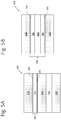
- Figure 5A is a partial cross-sectional view of a memory cell 300.
- the memory cell 300 includes a selector as shown in one of the figures above, in particular a selector as shown in figure 4A .
- the memory cell 300 further comprises a storage unit 400 for storing a bit in connection to the diode.
- the storage unit may be arranged to and in contact with one of the electrodes 110, 120 and a further electrode 130.
- a storage unit 400' may be provided in the intermediate layer stack 390' of a selector as shown in figure 4B between a bottom layer 280 of a semiconductor material or octadecyltrichlorosilane, OTS, and a top layer 285 of a semiconductor material or OTS.
- the semiconductor material may for example be indium gallium zinc oxide, IGZO.
- Figure 6 is schematic perspective view of a random access memory, RAM, having a crossbar architecture having memory cell with a MSM back-to-back Schottky diode.
- a crossbar memory architecture is a matrix of memory cells 300', with electrical contacts arranged along X-axes (i.e., word lines 310) and along y-axes (i.e., bit lines 320).
- a digital value may be stored as a memory resistance (high or low).
- the memory state of a memory cell can be read by supplying a voltage to the word line connected to the selected memory element.
- the resistance or memory state can be read either as an output voltage or current of the bit line connected to the selected memory cell.
- the RAM may be a resistive random access memory, RRAM, a magnetic random access memory, MRAM, a phase change random access memory, PC RAM, or a conducting bridge random access memory, CB RAM.
- RRAM resistive random access memory
- MRAM magnetic random access memory
- PC RAM phase change random access memory
- CB RAM conducting bridge random access memory
- FIG. 6 the combination of a memory cell 300' and a selector is shown as a block-shaped structure. The structure may for example be as shown in Fig. 5 , with the top electrode 120 forming the word line 310 and the bottom electrode 110 forming the word line 320.
- the selectors of Figs. 1-4 may be used within the scope of the present disclosure.
Landscapes
- Chemical & Material Sciences (AREA)
- Engineering & Computer Science (AREA)
- Materials Engineering (AREA)
- Semiconductor Memories (AREA)
- Electrodes Of Semiconductors (AREA)
Abstract
Description
- The present invention relates to a memory selector, in particular to a memory selector for a crossbar memory architecture, having a metal-semiconductor-metal, MSM, back-to-back Schottky diode. The present invention further relates to a random access memory, RAM, and a memory cell thereof.
- A typical random access memory having a crossbar architecture includes an array of memory cells, a plurality of parallel word lines extending along columns (or rows) of the memory cells, and a plurality of parallel bit lines extending along rows (or columns) of the memory cells. The word and bit lines overlie each other but are spaced from each other in a vertical direction. Each memory cell is located at a cross-point of a word line and a bit line, and typically includes a single memory selector in series with a storage unit for storing a bit. The memory selector and storage unit connected in series are electrically coupled to the word line at one terminal and to the bit line at the opposite terminal.
- A back-to-back Schottky diode is a device that permits current flow in both forward and reverse directions under higher voltage (forward and reverse) bias conditions, but blocks current in under lower voltage bias conditions. The use of back-to-back Schottky diodes as a memory selector in random access memory arrays is known. For example, this has been disclosed in
Sheng et al (U.S. Pat. No. 7,303,971 ) for resistance random access memory, RRAM, andLupino et al. (U.S. Pat. No. 8,952,470 ) for magnetic random access memory, MRAM. - A metal-semiconductor-metal, MSM, back-to-back Schottky diode includes a metal bottom electrode, a metal top electrode and selector material arranged in-between and in contact with the electrodes. A bottom Schottky barrier with a bottom Schottky barrier height ΦB is formed at the interface between the metal bottom electrode and the intermediate layer stack. A top Schottky barrier with a top Schottky barrier height ΦT is formed at the interface between the metal top electrode and the intermediate layer stack.
- It is an aim of the present disclosure is to provide an improved memory selector.
- It may be an aim of the present disclosure to prevent metal diffusion, to prevent thickness variation or to suppress thermal crosstalk. Additional and alternative aims may be understood from the following.
- The present disclosure provides a memory selector, for use in a crossbar memory architecture, having a metal-semiconductor-metal, MSM, back-to-back Schottky diode, said diode consisting of: a metal bottom electrode, a metal top electrode and an intermediate layer stack arranged in-between and in contact with the electrodes; a bottom Schottky barrier having a bottom Schottky barrier height ΦB formed at the interface between the metal bottom electrode and the intermediate layer stack; and a top Schottky barrier having a top Schottky barrier height ΦT formed at the interface between the metal top electrode and the intermediate layer stack. According to the present disclosure, the intermediate layer stack comprises one or more atomic layers of at least one two-dimensional, 2D, material at the interface with at least one of the electrodes, each atomic layer forming or modulating the respective Schottky barrier height.
- The present disclosure provides a single-layer or few layers of at least one two-dimensional, 2D, material at the interface with the metal bottom electrode and/or the metal top electrode. The two-dimensional material may be selected from the group consisting of a two-dimensional semiconductor material, a two-dimensional insulator material, and any other suitable 2D-material. One example of a 2D material is transition metal dichalcogenides (or TMD), denoted by MX2 with M a transition metal and X a chalcogenide. Examples of MX2 material are for example WS2, MoS2, WSe2, MoSe2, WTe2, MoTe2.
- For the purposes of this disclosure, the term "single-layer" refers to a 1 atomic layer (monolayer) whereas "few layers" refers to a layered structure with 2-10 layers of atoms. Each atomic layer forms or modulates respectively the bottom Schottky barrier height ΦB or the top Schottky barrier height ΦT.
- According to the present disclosure, the presence of a 2D material at the interface with the metal may provide a barrier layer to improve the prevention of metal diffusion into the selector material, thickness induced characteristic variation, and/or thermal crosstalk in the vertical direction. Due to the nonlinear current-voltage (IV) characteristic, the 2D material is preferably a 2D semiconductor that may be used as the selector material forming a Schottky barrier. This may further eliminate the need for high temperature processing such that it is compatible with back end of line, BEOL, process. Advantageously, the fabrication cost may be reduced.
- In a first aspect, which may be combined with the other aspects and embodiments described herein, the atomic layers are barrier formation layers. Each barrier formation layer is adapted to influence, e.g. increase or decrease, the respective Schottky barrier height between the respective electrode and a semiconductor layer present in the intermediate layer stack. The semiconductor material may be selected from the group consisting of two-dimensional semiconductor material, silicon, Si, indium gallium zinc oxide, IGZO, octadecyltrichlorosilane, OTS, and any other suitable oxide.
- In an embodiment according to the disclosure, the one or more atomic layers comprise multiple layers of different two-dimensional materials. For example, the different two-dimensional materials may comprise graphene and a 2D semiconductor material.
- In a second aspect, which may be combined with the other aspects and embodiments described herein, the intermediate layer stack comprises one or more atomic layers of at least one two-dimensional, 2D, material at the interface with the metal bottom electrode and the metal top electrode. Therefore, the atomic layers comprise one or more bottom layers at the interface with the bottom electrode and one or more top layers at the interface with the top electrode.
- In an embodiment according to the disclosure, the at least one two-dimensional bottom material and the at least one two-dimensional top material comprise the same two-dimensional materials.
- In another embodiment according to the disclosure, the at least one two-dimensional bottom material and the at least one two-dimensional top material comprise different two-dimensional materials.
- In embodiments according to the disclosure, the back-to-back Schottky diode comprises symmetric or asymmetric Schottky barrier heights. The bottom Schottky barrier height ΦB may be in the range of 0.1 eV to 1.0 eV, in particular in the range of 0.25 eV to 0.75 eV. The top Schottky barrier height ΦT may be in the range of 0.1 eV to 1.0 eV, in particular in the range of 0.25 eV to 0.75 eV.
- In a third aspect, which may be combined with the other aspects and embodiments described herein, the intermediate layer stack consists of exactly one layer of 2D-material, said 2D-material being a 2D-material semiconductor forming the bottom Schottky barrier of the metal bottom electrode and a top Schottky barrier of the metal top electrode.
- The present disclosure further relates to a memory cell comprising a storage unit for storing a bit and a memory selector as described above for controlling the access to the storage unit. The storage unit may be in contact with the metal bottom electrode or the metal top electrode, or the storage unit may be interposed in the semiconductor layer.
- The present disclosure further relates to a random access memory, RAM, having a crossbar architecture comprising a plurality of memory cells as described above, wherein the RAM is one selected from the group consisting of resistive random access memory, RRAM, magnetic random access memory, MRAM, phase change random access memory, PC RAM, and conducting bridge random access memory, CB RAM.
- The invention will be explained in more detail below with reference to drawings in which illustrative embodiments thereof are shown. They are intended exclusively for illustrative purposes and not to restrict the inventive concept, which is defined by the appended claims.
-
Figure 1 is a partial cross-sectional view of an embodiment of a metal-semiconductor-metal, MSM, back-to-back Schottky diode according to the present disclosure; -
Figures 2A and 2B are partial cross-sectional views of an alternative embodiment of the back-to-back Schottky diode offigure 1 ; -
Figure 3 is partial cross-sectional view of another alternative embodiment of the back-to-back Schottky diode offigure 1 ; -
Figures 4A and 4B are partial cross-sectional views of a further alternative embodiment of the back-to-back Schottky diode offigure 3 ; -
Figure 5A and 5B are partial cross-sectional views of embodiments of a memory cell with a MSM back-to-back Schottky diode according to the present disclosure; and -
Figure 6 is schematic view of a random access memory, RAM, having a crossbar architecture having memory cell with an MSM back-to-back Schottky diode, according to the present disclosure. - The present invention will be described with respect to particular embodiments and with reference to certain drawings but the invention is not limited thereto but only by the claims. The drawings described are only schematic and are non-limiting. In the drawings, the size of some of the elements may be exaggerated and not drawn on scale for illustrative purposes. The dimensions and the relative dimensions do not necessarily correspond to actual reductions to practice of the invention.
- Furthermore, the terms first, second, third and the like in the description and in the claims, are used for distinguishing between similar elements and not necessarily for describing a sequential or chronological order. The terms are interchangeable under appropriate circumstances and the embodiments of the invention can operate in other sequences than described or illustrated herein.
- Moreover, the terms top, bottom, over, under and the like in the description and the claims are used for descriptive purposes and not necessarily for describing relative positions. The terms so used are interchangeable under appropriate circumstances and the embodiments of the invention described herein can operate in other orientations than described or illustrated herein.
- Furthermore, the various embodiments, although referred to as "preferred" are to be construed as exemplary manners in which the invention may be implemented rather than as limiting the scope of the invention.
- The term "comprising", used in the claims, should not be interpreted as being restricted to the elements or steps listed thereafter; it does not exclude other elements or steps. It needs to be interpreted as specifying the presence of the stated features, integers, steps or components as referred to, but does not preclude the presence or addition of one or more other features, integers, steps or components, or groups thereof. Thus, the scope of the expression "a device comprising A and B" should not be limited to devices consisting only of components A and B, rather with respect to the present invention, the only enumerated components of the device are A and B, and further the claim should be interpreted as including equivalents of those components.
-
Figure 1 is a partial cross-sectional view of a metal/semiconductor/metal, MSM, back-to-back Schottky diode. The back-to-back Schottky diode 100 is a vertical diode of ametal bottom electrode 110, ametal top electrode 120 and anintermediate layer stack 200 arranged in-between and in contact with theelectrodes
Themetal top electrode 120 and themetal bottom electrode 110 form respectively a top Schottky barrier having a top Schottky barrier height ΦT and a bottom Schottky barrier having a bottom Schottky barrier height ΦB.
Theintermediate layer stack 200 comprises at least one layer. In the embodiment shown inFig. 1 , thestack 200 comprises abottom layer 201 of a two-dimensional, 2D, material arranged in contact with thebottom electrode 110. Alternatively, or in combination, thestack 200 could also comprise a top layer of a two-dimensional, 2D, material arranged in contact with thetop electrode 120. - In the embodiments described herein, the
metal top electrode 120 and themetal bottom electrode 110 may be made of materials such as Pt, Au, Ag, Ru, TiN, Ta, or TaN. However, other materials that are well known in the art for use as a conductive electrode, may also be used for the top and/or bottom electrodes. In embodiments, themetal top electrode 120 andmetal bottom electrode 110 are the same material and, therefore, have identical work functions. Work function is a measure of the minimum energy, as expressed in electron volts (eV), needed to remove an electron from the Fermi level in a metal, to a far point. - The 2D-material may be a two-dimensional semiconductor material, a two-dimensional insulator material, or any other suitable 2D-material such as graphene. In particular, when the two-dimensional material is a two-dimensional semiconductor material, the material may be molybdenite, MoS2, or any other suitable material.
- In the embodiments described herein, the
intermediate layer stack 200 may have a thickness in the range of about 0.6 nanometers, nm, to 12.0 nm, in particular about 6.0 nm. Themetal top electrode 120 andmetal bottom electrode 110 may each have a thickness in the range of about 1.0 to 100.0 nm. Themetal top electrode 120 need not necessarily be the same thickness as themetal bottom electrode 110. -
Figures 2A and 2B are partial cross-sectional views of alternatives of the back-to-back Schottky diode offigure 1 . TheseSchottky diodes 100', 100" include all the elements of the diode shown infigure 1 , wherein theintermediate layer stack 200', 200" comprises at least onesemiconductor layer 205; 210, 220 of a two-dimensional, 2D, semiconductor material arranged in-between and in contact with at least one of theelectrodes
In the embodiment depicted infigure 2A , theintermediate layer stack 200 consists of asingle layer 205 of 2D semiconductor material, saidlayer 205 forming the bottom Schottky barrier and the top Schottky barrier.
In the embodiment depicted infigure 2B , theintermediate layer stack 200 consists of a few layers comprising abottom layer 210 of a 2D semiconductor material at the interface with the metal bottom electrode, saidbottom layer 210 forming the bottom Schottky barrier, and atop layer 220 of a 2D semiconductor material at the interface with the metal top electrode, saidtop layer 220 forming the top Schottky barrier. Thebottom layer 210 and thetop layer 220 may be made of different two-dimensional semiconductor materials. The 2D semiconductor material may be molybdenite, MoS2, MoSe2, WS2, WSe2, GaSe, GaTe, FeTe, or any other suitable material. -
Figure 3 is a partial cross-sectional view of another alternative of the back-to-back Schottky diode offigure 1 . This alternative of the Schottky diode 100'" includes all the elements of the diode shown infigure 1 , wherein the intermediate layer stack 200'" comprises at least one barrierformation layer stack 230 of 2D material arranged in-between and in contact with at least one of theelectrodes 110; 120, said at least one barrierformation layer stack 230 being adapted to influence, e.g. increase or decrease, the Schottky barrier between asemiconductor layer 210; 250 and the respective electrode. In embodiments, the barrierformation layer stack 230 may comprise a single layer of 2D material or a few layers of 2D material. -
Figures 4A and 4B are partial cross-sectional views of further alternatives of the back-to-back Schottky diode offigure 3 . These alternatives of theSchottky diode 150; 150' include all the elements of the diode shown infigure 3 , wherein theintermediate layer stack 290; 290' comprises a bottom barrierformation layer stack 230 of 2D material at the interface with the metal bottom electrode and a top barrierformation layer stack 240 of 2D material at the interface with the metal top electrode.
In the embodiment depicted infigure 4A , theintermediate layer stack 290 consists of asingle layer 270 of 2D semiconductor material, saidsemiconductor layer 270 being arranged in-between and in contact with the bottom barrierformation layer stack 230 and the top barrierformation layer stack 240.
In the embodiment depicted infigure 4B , the intermediate layer stack 290' comprises abottom layer 280 of a semiconductor material forming the bottom Schottky barrier and atop layer 285 of a semiconductor material forming the top Schottky barrier. In between the bottom and top layers ofsemiconductor material semiconductor material -
Figure 5A is a partial cross-sectional view of amemory cell 300. Thememory cell 300 includes a selector as shown in one of the figures above, in particular a selector as shown infigure 4A . Thememory cell 300 further comprises astorage unit 400 for storing a bit in connection to the diode. The storage unit may be arranged to and in contact with one of theelectrodes further electrode 130. - Alternatively, as shown in
figure 5B , a storage unit 400' may be provided in the intermediate layer stack 390' of a selector as shown infigure 4B between abottom layer 280 of a semiconductor material or octadecyltrichlorosilane, OTS, and atop layer 285 of a semiconductor material or OTS. The semiconductor material may for example be indium gallium zinc oxide, IGZO. -
Figure 6 is schematic perspective view of a random access memory, RAM, having a crossbar architecture having memory cell with a MSM back-to-back Schottky diode. A crossbar memory architecture is a matrix of memory cells 300', with electrical contacts arranged along X-axes (i.e., word lines 310) and along y-axes (i.e., bit lines 320). In embodiments, a digital value may be stored as a memory resistance (high or low). The memory state of a memory cell can be read by supplying a voltage to the word line connected to the selected memory element. The resistance or memory state can be read either as an output voltage or current of the bit line connected to the selected memory cell. In embodiments, the RAM may be a resistive random access memory, RRAM, a magnetic random access memory, MRAM, a phase change random access memory, PC RAM, or a conducting bridge random access memory, CB RAM.
InFigure 6 , the combination of a memory cell 300' and a selector is shown as a block-shaped structure. The structure may for example be as shown inFig. 5 , with thetop electrode 120 forming theword line 310 and thebottom electrode 110 forming theword line 320. In alternative embodiments, the selectors ofFigs. 1-4 , or other selectors as disclosed herein, may be used within the scope of the present disclosure.
Claims (15)
- Memory selector, for use in a crossbar memory architecture, having a metal-semiconductor-metal, MSM, back-to-back Schottky diode, said diode consisting of:a metal bottom electrode (110), a metal top electrode (120) and an intermediate layer stack (200) arranged in-between and in contact with the electrodes (110, 120);a bottom Schottky barrier having a bottom Schottky barrier height ΦB formed at the interface between the metal bottom electrode (110) and the intermediate layer stack (200); anda top Schottky barrier having a top Schottky barrier height ΦT formed at the interface between the metal top electrode (120) and the intermediate layer stack (200), characterised in, that the intermediate layer stack (200) comprises one or more atomic layers (210, 220, 230, 240) of at least one two-dimensional, 2D, material at the interface with at least one of the electrodes (110; 120), each atomic layer (210, 220, 230, 240) forming or modulating the respective Schottky barrier height.
- Memory selector according to claim 1, wherein the atomic layers are barrier formation layers (230, 240), each barrier formation layer (230) being adapted to form or modulate the respective Schottky barrier height between the respective electrode (110) and a semiconductor layer (210; 220; 250; 260) of a semiconductor material in the intermediate layer stack (200).
- Memory selector according to claim 1 or claim 2, wherein the atomic layers comprise multiple layers of different two-dimensional materials.
- Memory selector according to any one of the preceding claims, wherein the intermediate layer stack (200) comprises one or more atomic layers (210, 220, 230, 240) of at least one two-dimensional, 2D, material at the interface with each of the electrodes (110, 120), said one or more atomic layers comprising:one or more bottom layers (210, 230) of at least one two-dimensional, 2D, bottom material at the interface with the bottom electrode (110), said bottom layer (210, 230) forming or modulating the bottom Schottky barrier height ΦB; andone or more top layers (220, 240) of at least one two-dimensional, 2D, top material at the interface with the top electrode (120), said top layer (220, 240) forming or modulating the top Schottky barrier height ΦT.
- Memory selector according to claim 4, wherein the at least one two-dimensional bottom material and the at least one two-dimensional top material comprise the same two-dimensional materials.
- Memory selector according to claim 4, wherein the at least one two-dimensional bottom material and the at least one two-dimensional top material comprise different two-dimensional materials.
- Memory selector according to any one of the preceding claims, wherein the back-to-back Schottky diode comprises symmetric or asymmetric Schottky barrier heights.
- Memory selector according to any one of the preceding claims,
wherein the bottom Schottky barrier height ΦB is in the range of 0.1 eV to 1.0 eV, and/or
wherein the top Schottky barrier height ΦT is in the range of 0.1 eV to 1.0 eV. - Memory selector according to any one of the preceding claims, wherein the two-dimensional material is selected from the group consisting of a two-dimensional semiconductor material, a two-dimensional insulator material, and any other suitable 2D-material.
- Memory selector according to claim 8 or 9, wherein the two-dimensional semiconductor material is molybdenite, MoS2, MoSe2, WS2, WSe2, GaSe, GaTe, FeTe, or any other suitable material.
- Memory selector according to claim 1, wherein the intermediate layer stack (200) consist of exactly one layer of 2D-material, said 2D-material being a 2D-material semiconductor forming the bottom Schottky barrier of the metal bottom electrode and a top Schottky barrier of the metal top electrode.
- Memory cell comprising a storage unit for storing a bit and a memory selector according to any one of the preceding claims for controlling the access to the storage unit.
- Memory cell according to claim 12, wherein the storage unit is in contact with the metal bottom electrode or the metal top electrode.
- Memory cell according to claim 12, comprising a memory selector according to claim 2, wherein the storage unit is interposed in the semiconductor layer (210; 220; 250; 260).
- Random access memory, RAM, having a crossbar architecture comprising at least two memory cells according to any one of the preceding claims 12 - 14, wherein the RAM is one selected from the group consisting of resistive random access memory, RRAM, magnetic random access memory, MRAM, phase change random access memory, PC RAM, and conducting bridge random access memory, CB RAM.
Priority Applications (2)
| Application Number | Priority Date | Filing Date | Title |
|---|---|---|---|
| EP18192451.5A EP3621122B1 (en) | 2018-09-04 | 2018-09-04 | Memory selector, memory cell and random access memory |
| US16/559,501 US11374058B2 (en) | 2018-09-04 | 2019-09-03 | Memory selector and memory device including same |
Applications Claiming Priority (1)
| Application Number | Priority Date | Filing Date | Title |
|---|---|---|---|
| EP18192451.5A EP3621122B1 (en) | 2018-09-04 | 2018-09-04 | Memory selector, memory cell and random access memory |
Publications (2)
| Publication Number | Publication Date |
|---|---|
| EP3621122A1 true EP3621122A1 (en) | 2020-03-11 |
| EP3621122B1 EP3621122B1 (en) | 2021-11-17 |
Family
ID=63517674
Family Applications (1)
| Application Number | Title | Priority Date | Filing Date |
|---|---|---|---|
| EP18192451.5A Active EP3621122B1 (en) | 2018-09-04 | 2018-09-04 | Memory selector, memory cell and random access memory |
Country Status (2)
| Country | Link |
|---|---|
| US (1) | US11374058B2 (en) |
| EP (1) | EP3621122B1 (en) |
Families Citing this family (11)
| Publication number | Priority date | Publication date | Assignee | Title |
|---|---|---|---|---|
| KR20210068796A (en) * | 2019-12-02 | 2021-06-10 | 삼성전자주식회사 | Variable resistance memory devices |
| CN111554809A (en) * | 2020-05-15 | 2020-08-18 | 中国科学院微电子研究所 | Two-dimensional material-based gates, memory cells, arrays, and methods of operating the same |
| WO2021114571A1 (en) * | 2020-05-15 | 2021-06-17 | 中国科学院微电子研究所 | Two-dimensional material-based gate, memory unit, array, and operating method thereof |
| US11342380B2 (en) * | 2020-05-27 | 2022-05-24 | Taiwan Semiconductor Manufacturing Company, Ltd. | Memory devices with selector layer and methods of forming the same |
| CN111740011A (en) * | 2020-06-24 | 2020-10-02 | 中国科学院微电子研究所 | Spin-orbit torque magnetic random access memory cells, memory arrays and memories |
| US20230276637A1 (en) * | 2020-06-24 | 2023-08-31 | Institute of Microelectronics, Chinese Academy of Sciences | Spin orbit torque magnetic random access memory cell, memory array, and memory |
| US11430512B2 (en) | 2020-06-29 | 2022-08-30 | Taiwan Semiconductor Manufacturing Company Limited | Semiconducting metal oxide memory device using hydrogen-mediated threshold voltage modulation and methods for forming the same |
| US11588105B2 (en) | 2021-03-11 | 2023-02-21 | International Business Machines Corporation | Phase-change memory device with reduced programming voltage |
| CN113793899B (en) * | 2021-08-20 | 2023-07-04 | 华中科技大学 | Selector performance optimization method based on regulation and control of conductive wire growth and application |
| KR20230085735A (en) | 2021-12-07 | 2023-06-14 | 에스케이하이닉스 주식회사 | Electronic device and method for fabricating the same |
| US11996145B2 (en) | 2022-05-03 | 2024-05-28 | Western Digital Technologies, Inc. | Cross-point array with threshold switching selector memory element |
Citations (4)
| Publication number | Priority date | Publication date | Assignee | Title |
|---|---|---|---|---|
| US7303971B2 (en) | 2005-07-18 | 2007-12-04 | Sharp Laboratories Of America, Inc. | MSM binary switch memory device |
| US8952470B2 (en) | 2012-09-10 | 2015-02-10 | James John Lupino | Low cost high density nonvolatile memory array device employing thin film transistors and back to back Schottky diodes |
| US20150333196A1 (en) * | 2014-05-19 | 2015-11-19 | Research & Business Foundation Sungkyunkwan University | Optoelectronic device including ferroelectric material |
| WO2016068745A1 (en) * | 2014-10-31 | 2016-05-06 | Nokia Technologies Oy | Memory apparatus and method of production thereof |
Family Cites Families (11)
| Publication number | Priority date | Publication date | Assignee | Title |
|---|---|---|---|---|
| US8879299B2 (en) * | 2011-10-17 | 2014-11-04 | Sandisk 3D Llc | Non-volatile memory cell containing an in-cell resistor |
| US20140264224A1 (en) * | 2013-03-14 | 2014-09-18 | Intermolecular, Inc. | Performance Enhancement of Forming-Free ReRAM Devices Using 3D Nanoparticles |
| WO2015107945A1 (en) * | 2014-01-17 | 2015-07-23 | ソニー株式会社 | Switch element and memory device |
| US20160149129A1 (en) * | 2014-11-25 | 2016-05-26 | Intermolecular, Inc. | Using Metal Silicides as Electrodes for MSM Stack in Selector for Non-Volatile Memory Application |
| WO2018004587A1 (en) | 2016-06-30 | 2018-01-04 | Intel Corporation | Rram devices with two-dimensional thermal barrier layers |
| US10008665B1 (en) * | 2016-12-27 | 2018-06-26 | Intel Corporation | Doping of selector and storage materials of a memory cell |
| US10872660B2 (en) * | 2016-12-30 | 2020-12-22 | Intel Corporation | Resistive memory devices with transition metal dichalcogenide (TMD) materials as ballast resistors to control current flow through the devices |
| US11145737B2 (en) * | 2017-09-26 | 2021-10-12 | Intel Corporation | Selector devices |
| KR102496377B1 (en) * | 2017-10-24 | 2023-02-06 | 삼성전자주식회사 | Apparatus of Nonvolatile memory including resistive-change material layer |
| US10269442B1 (en) * | 2017-12-28 | 2019-04-23 | Micron Technology, Inc. | Drift mitigation with embedded refresh |
| US11665975B2 (en) * | 2018-06-19 | 2023-05-30 | Intel Corporation | Spin orbit coupling memory device with top spin orbit coupling electrode and selector |
-
2018
- 2018-09-04 EP EP18192451.5A patent/EP3621122B1/en active Active
-
2019
- 2019-09-03 US US16/559,501 patent/US11374058B2/en active Active
Patent Citations (4)
| Publication number | Priority date | Publication date | Assignee | Title |
|---|---|---|---|---|
| US7303971B2 (en) | 2005-07-18 | 2007-12-04 | Sharp Laboratories Of America, Inc. | MSM binary switch memory device |
| US8952470B2 (en) | 2012-09-10 | 2015-02-10 | James John Lupino | Low cost high density nonvolatile memory array device employing thin film transistors and back to back Schottky diodes |
| US20150333196A1 (en) * | 2014-05-19 | 2015-11-19 | Research & Business Foundation Sungkyunkwan University | Optoelectronic device including ferroelectric material |
| WO2016068745A1 (en) * | 2014-10-31 | 2016-05-06 | Nokia Technologies Oy | Memory apparatus and method of production thereof |
Non-Patent Citations (1)
| Title |
|---|
| HOON HAHN YOON ET AL: "Strong Fermi-Level Pinning at Metal/n-Si(001) Interface Ensured by Forming an Intact Schottky Contact with a Graphene Insertion Layer", NANO LETTERS, vol. 17, no. 1, 19 December 2016 (2016-12-19), US, pages 44 - 49, XP055553033, ISSN: 1530-6984, DOI: 10.1021/acs.nanolett.6b03137 * |
Also Published As
| Publication number | Publication date |
|---|---|
| EP3621122B1 (en) | 2021-11-17 |
| US11374058B2 (en) | 2022-06-28 |
| US20200075676A1 (en) | 2020-03-05 |
Similar Documents
| Publication | Publication Date | Title |
|---|---|---|
| EP3621122B1 (en) | Memory selector, memory cell and random access memory | |
| US8642985B2 (en) | Memory Cell | |
| US9831287B2 (en) | Memory devices and memory device forming methods | |
| US9825091B2 (en) | Memory cell structures | |
| EP2279523B1 (en) | Resistance switching memory cell | |
| US9923027B2 (en) | Structure and method for memory cell array | |
| KR101943721B1 (en) | Switching components and memory units | |
| US20050254291A1 (en) | Semiconductor memory component in cross-point architecture | |
| US20130163323A1 (en) | Semiconductor memory device using variable resistance element or phase-change element as memory device | |
| US8295123B2 (en) | Current rectifying element, memory device incorporating current rectifying element, and fabrication method thereof | |
| US20110068314A1 (en) | Semiconductor memory device | |
| US20120305878A1 (en) | Resistive switching memory device | |
| US20150137062A1 (en) | Mimcaps with quantum wells as selector elements for crossbar memory arrays | |
| US11018189B2 (en) | Storage apparatus | |
| KR101955133B1 (en) | Devices containing metal chalcogenides | |
| US20210005252A1 (en) | Cross point device and storage apparatus | |
| US12432931B2 (en) | Memory cell including two selectors and method of making same | |
| US11856879B2 (en) | MIEC and tunnel-based selectors with improved rectification characteristics and tunability | |
| US20230134429A1 (en) | Semiconductor device and method for fabricating the same |
Legal Events
| Date | Code | Title | Description |
|---|---|---|---|
| PUAI | Public reference made under article 153(3) epc to a published international application that has entered the european phase |
Free format text: ORIGINAL CODE: 0009012 |
|
| STAA | Information on the status of an ep patent application or granted ep patent |
Free format text: STATUS: THE APPLICATION HAS BEEN PUBLISHED |
|
| AK | Designated contracting states |
Kind code of ref document: A1 Designated state(s): AL AT BE BG CH CY CZ DE DK EE ES FI FR GB GR HR HU IE IS IT LI LT LU LV MC MK MT NL NO PL PT RO RS SE SI SK SM TR |
|
| AX | Request for extension of the european patent |
Extension state: BA ME |
|
| STAA | Information on the status of an ep patent application or granted ep patent |
Free format text: STATUS: REQUEST FOR EXAMINATION WAS MADE |
|
| 17P | Request for examination filed |
Effective date: 20200902 |
|
| RBV | Designated contracting states (corrected) |
Designated state(s): AL AT BE BG CH CY CZ DE DK EE ES FI FR GB GR HR HU IE IS IT LI LT LU LV MC MK MT NL NO PL PT RO RS SE SI SK SM TR |
|
| GRAP | Despatch of communication of intention to grant a patent |
Free format text: ORIGINAL CODE: EPIDOSNIGR1 |
|
| STAA | Information on the status of an ep patent application or granted ep patent |
Free format text: STATUS: GRANT OF PATENT IS INTENDED |
|
| RIC1 | Information provided on ipc code assigned before grant |
Ipc: H01L 29/872 20060101AFI20210622BHEP Ipc: H01L 29/267 20060101ALI20210622BHEP Ipc: H01L 27/24 20060101ALI20210622BHEP Ipc: H01L 29/06 20060101ALI20210622BHEP Ipc: H01L 29/24 20060101ALI20210622BHEP |
|
| INTG | Intention to grant announced |
Effective date: 20210709 |
|
| GRAS | Grant fee paid |
Free format text: ORIGINAL CODE: EPIDOSNIGR3 |
|
| GRAA | (expected) grant |
Free format text: ORIGINAL CODE: 0009210 |
|
| STAA | Information on the status of an ep patent application or granted ep patent |
Free format text: STATUS: THE PATENT HAS BEEN GRANTED |
|
| AK | Designated contracting states |
Kind code of ref document: B1 Designated state(s): AL AT BE BG CH CY CZ DE DK EE ES FI FR GB GR HR HU IE IS IT LI LT LU LV MC MK MT NL NO PL PT RO RS SE SI SK SM TR |
|
| REG | Reference to a national code |
Ref country code: GB Ref legal event code: FG4D |
|
| REG | Reference to a national code |
Ref country code: IE Ref legal event code: FG4D |
|
| REG | Reference to a national code |
Ref country code: DE Ref legal event code: R096 Ref document number: 602018026735 Country of ref document: DE |
|
| REG | Reference to a national code |
Ref country code: AT Ref legal event code: REF Ref document number: 1448778 Country of ref document: AT Kind code of ref document: T Effective date: 20211215 |
|
| REG | Reference to a national code |
Ref country code: LT Ref legal event code: MG9D |
|
| REG | Reference to a national code |
Ref country code: NL Ref legal event code: MP Effective date: 20211117 |
|
| REG | Reference to a national code |
Ref country code: AT Ref legal event code: MK05 Ref document number: 1448778 Country of ref document: AT Kind code of ref document: T Effective date: 20211117 |
|
| PG25 | Lapsed in a contracting state [announced via postgrant information from national office to epo] |
Ref country code: RS Free format text: LAPSE BECAUSE OF FAILURE TO SUBMIT A TRANSLATION OF THE DESCRIPTION OR TO PAY THE FEE WITHIN THE PRESCRIBED TIME-LIMIT Effective date: 20211117 Ref country code: LT Free format text: LAPSE BECAUSE OF FAILURE TO SUBMIT A TRANSLATION OF THE DESCRIPTION OR TO PAY THE FEE WITHIN THE PRESCRIBED TIME-LIMIT Effective date: 20211117 Ref country code: FI Free format text: LAPSE BECAUSE OF FAILURE TO SUBMIT A TRANSLATION OF THE DESCRIPTION OR TO PAY THE FEE WITHIN THE PRESCRIBED TIME-LIMIT Effective date: 20211117 Ref country code: BG Free format text: LAPSE BECAUSE OF FAILURE TO SUBMIT A TRANSLATION OF THE DESCRIPTION OR TO PAY THE FEE WITHIN THE PRESCRIBED TIME-LIMIT Effective date: 20220217 Ref country code: AT Free format text: LAPSE BECAUSE OF FAILURE TO SUBMIT A TRANSLATION OF THE DESCRIPTION OR TO PAY THE FEE WITHIN THE PRESCRIBED TIME-LIMIT Effective date: 20211117 |
|
| PG25 | Lapsed in a contracting state [announced via postgrant information from national office to epo] |
Ref country code: IS Free format text: LAPSE BECAUSE OF FAILURE TO SUBMIT A TRANSLATION OF THE DESCRIPTION OR TO PAY THE FEE WITHIN THE PRESCRIBED TIME-LIMIT Effective date: 20220317 Ref country code: SE Free format text: LAPSE BECAUSE OF FAILURE TO SUBMIT A TRANSLATION OF THE DESCRIPTION OR TO PAY THE FEE WITHIN THE PRESCRIBED TIME-LIMIT Effective date: 20211117 Ref country code: PT Free format text: LAPSE BECAUSE OF FAILURE TO SUBMIT A TRANSLATION OF THE DESCRIPTION OR TO PAY THE FEE WITHIN THE PRESCRIBED TIME-LIMIT Effective date: 20220317 Ref country code: PL Free format text: LAPSE BECAUSE OF FAILURE TO SUBMIT A TRANSLATION OF THE DESCRIPTION OR TO PAY THE FEE WITHIN THE PRESCRIBED TIME-LIMIT Effective date: 20211117 Ref country code: NO Free format text: LAPSE BECAUSE OF FAILURE TO SUBMIT A TRANSLATION OF THE DESCRIPTION OR TO PAY THE FEE WITHIN THE PRESCRIBED TIME-LIMIT Effective date: 20220217 Ref country code: NL Free format text: LAPSE BECAUSE OF FAILURE TO SUBMIT A TRANSLATION OF THE DESCRIPTION OR TO PAY THE FEE WITHIN THE PRESCRIBED TIME-LIMIT Effective date: 20211117 Ref country code: LV Free format text: LAPSE BECAUSE OF FAILURE TO SUBMIT A TRANSLATION OF THE DESCRIPTION OR TO PAY THE FEE WITHIN THE PRESCRIBED TIME-LIMIT Effective date: 20211117 Ref country code: HR Free format text: LAPSE BECAUSE OF FAILURE TO SUBMIT A TRANSLATION OF THE DESCRIPTION OR TO PAY THE FEE WITHIN THE PRESCRIBED TIME-LIMIT Effective date: 20211117 Ref country code: GR Free format text: LAPSE BECAUSE OF FAILURE TO SUBMIT A TRANSLATION OF THE DESCRIPTION OR TO PAY THE FEE WITHIN THE PRESCRIBED TIME-LIMIT Effective date: 20220218 Ref country code: ES Free format text: LAPSE BECAUSE OF FAILURE TO SUBMIT A TRANSLATION OF THE DESCRIPTION OR TO PAY THE FEE WITHIN THE PRESCRIBED TIME-LIMIT Effective date: 20211117 |
|
| PG25 | Lapsed in a contracting state [announced via postgrant information from national office to epo] |
Ref country code: SM Free format text: LAPSE BECAUSE OF FAILURE TO SUBMIT A TRANSLATION OF THE DESCRIPTION OR TO PAY THE FEE WITHIN THE PRESCRIBED TIME-LIMIT Effective date: 20211117 Ref country code: SK Free format text: LAPSE BECAUSE OF FAILURE TO SUBMIT A TRANSLATION OF THE DESCRIPTION OR TO PAY THE FEE WITHIN THE PRESCRIBED TIME-LIMIT Effective date: 20211117 Ref country code: RO Free format text: LAPSE BECAUSE OF FAILURE TO SUBMIT A TRANSLATION OF THE DESCRIPTION OR TO PAY THE FEE WITHIN THE PRESCRIBED TIME-LIMIT Effective date: 20211117 Ref country code: EE Free format text: LAPSE BECAUSE OF FAILURE TO SUBMIT A TRANSLATION OF THE DESCRIPTION OR TO PAY THE FEE WITHIN THE PRESCRIBED TIME-LIMIT Effective date: 20211117 Ref country code: DK Free format text: LAPSE BECAUSE OF FAILURE TO SUBMIT A TRANSLATION OF THE DESCRIPTION OR TO PAY THE FEE WITHIN THE PRESCRIBED TIME-LIMIT Effective date: 20211117 Ref country code: CZ Free format text: LAPSE BECAUSE OF FAILURE TO SUBMIT A TRANSLATION OF THE DESCRIPTION OR TO PAY THE FEE WITHIN THE PRESCRIBED TIME-LIMIT Effective date: 20211117 |
|
| REG | Reference to a national code |
Ref country code: DE Ref legal event code: R097 Ref document number: 602018026735 Country of ref document: DE |
|
| PLBE | No opposition filed within time limit |
Free format text: ORIGINAL CODE: 0009261 |
|
| STAA | Information on the status of an ep patent application or granted ep patent |
Free format text: STATUS: NO OPPOSITION FILED WITHIN TIME LIMIT |
|
| 26N | No opposition filed |
Effective date: 20220818 |
|
| PG25 | Lapsed in a contracting state [announced via postgrant information from national office to epo] |
Ref country code: AL Free format text: LAPSE BECAUSE OF FAILURE TO SUBMIT A TRANSLATION OF THE DESCRIPTION OR TO PAY THE FEE WITHIN THE PRESCRIBED TIME-LIMIT Effective date: 20211117 |
|
| PG25 | Lapsed in a contracting state [announced via postgrant information from national office to epo] |
Ref country code: SI Free format text: LAPSE BECAUSE OF FAILURE TO SUBMIT A TRANSLATION OF THE DESCRIPTION OR TO PAY THE FEE WITHIN THE PRESCRIBED TIME-LIMIT Effective date: 20211117 |
|
| PG25 | Lapsed in a contracting state [announced via postgrant information from national office to epo] |
Ref country code: MC Free format text: LAPSE BECAUSE OF FAILURE TO SUBMIT A TRANSLATION OF THE DESCRIPTION OR TO PAY THE FEE WITHIN THE PRESCRIBED TIME-LIMIT Effective date: 20211117 |
|
| REG | Reference to a national code |
Ref country code: CH Ref legal event code: PL |
|
| GBPC | Gb: european patent ceased through non-payment of renewal fee |
Effective date: 20220904 |
|
| REG | Reference to a national code |
Ref country code: BE Ref legal event code: MM Effective date: 20220930 |
|
| PG25 | Lapsed in a contracting state [announced via postgrant information from national office to epo] |
Ref country code: IT Free format text: LAPSE BECAUSE OF FAILURE TO SUBMIT A TRANSLATION OF THE DESCRIPTION OR TO PAY THE FEE WITHIN THE PRESCRIBED TIME-LIMIT Effective date: 20211117 |
|
| P01 | Opt-out of the competence of the unified patent court (upc) registered |
Effective date: 20230513 |
|
| PG25 | Lapsed in a contracting state [announced via postgrant information from national office to epo] |
Ref country code: LU Free format text: LAPSE BECAUSE OF NON-PAYMENT OF DUE FEES Effective date: 20220904 |
|
| PG25 | Lapsed in a contracting state [announced via postgrant information from national office to epo] |
Ref country code: LI Free format text: LAPSE BECAUSE OF NON-PAYMENT OF DUE FEES Effective date: 20220930 Ref country code: IE Free format text: LAPSE BECAUSE OF NON-PAYMENT OF DUE FEES Effective date: 20220904 Ref country code: FR Free format text: LAPSE BECAUSE OF NON-PAYMENT OF DUE FEES Effective date: 20220930 Ref country code: CH Free format text: LAPSE BECAUSE OF NON-PAYMENT OF DUE FEES Effective date: 20220930 |
|
| PG25 | Lapsed in a contracting state [announced via postgrant information from national office to epo] |
Ref country code: BE Free format text: LAPSE BECAUSE OF NON-PAYMENT OF DUE FEES Effective date: 20220930 |
|
| PG25 | Lapsed in a contracting state [announced via postgrant information from national office to epo] |
Ref country code: GB Free format text: LAPSE BECAUSE OF NON-PAYMENT OF DUE FEES Effective date: 20220904 |
|
| PG25 | Lapsed in a contracting state [announced via postgrant information from national office to epo] |
Ref country code: HU Free format text: LAPSE BECAUSE OF FAILURE TO SUBMIT A TRANSLATION OF THE DESCRIPTION OR TO PAY THE FEE WITHIN THE PRESCRIBED TIME-LIMIT; INVALID AB INITIO Effective date: 20180904 |
|
| PG25 | Lapsed in a contracting state [announced via postgrant information from national office to epo] |
Ref country code: CY Free format text: LAPSE BECAUSE OF FAILURE TO SUBMIT A TRANSLATION OF THE DESCRIPTION OR TO PAY THE FEE WITHIN THE PRESCRIBED TIME-LIMIT Effective date: 20211117 |
|
| PG25 | Lapsed in a contracting state [announced via postgrant information from national office to epo] |
Ref country code: MK Free format text: LAPSE BECAUSE OF FAILURE TO SUBMIT A TRANSLATION OF THE DESCRIPTION OR TO PAY THE FEE WITHIN THE PRESCRIBED TIME-LIMIT Effective date: 20211117 |
|
| PG25 | Lapsed in a contracting state [announced via postgrant information from national office to epo] |
Ref country code: MT Free format text: LAPSE BECAUSE OF FAILURE TO SUBMIT A TRANSLATION OF THE DESCRIPTION OR TO PAY THE FEE WITHIN THE PRESCRIBED TIME-LIMIT Effective date: 20211117 |
|
| REG | Reference to a national code |
Ref country code: DE Ref legal event code: R079 Ref document number: 602018026735 Country of ref document: DE Free format text: PREVIOUS MAIN CLASS: H01L0029872000 Ipc: H10D0008600000 |
|
| PGFP | Annual fee paid to national office [announced via postgrant information from national office to epo] |
Ref country code: DE Payment date: 20250820 Year of fee payment: 8 |
|
| PG25 | Lapsed in a contracting state [announced via postgrant information from national office to epo] |
Ref country code: TR Free format text: LAPSE BECAUSE OF FAILURE TO SUBMIT A TRANSLATION OF THE DESCRIPTION OR TO PAY THE FEE WITHIN THE PRESCRIBED TIME-LIMIT Effective date: 20211117 |