EP3618275A1 - Impedance tuner and signal amplification device - Google Patents
Impedance tuner and signal amplification device Download PDFInfo
- Publication number
- EP3618275A1 EP3618275A1 EP17910949.1A EP17910949A EP3618275A1 EP 3618275 A1 EP3618275 A1 EP 3618275A1 EP 17910949 A EP17910949 A EP 17910949A EP 3618275 A1 EP3618275 A1 EP 3618275A1
- Authority
- EP
- European Patent Office
- Prior art keywords
- impedance
- variable reactance
- signal
- phase
- phase shifter
- Prior art date
- Legal status (The legal status is an assumption and is not a legal conclusion. Google has not performed a legal analysis and makes no representation as to the accuracy of the status listed.)
- Withdrawn
Links
Images


Classifications
-
- H—ELECTRICITY
- H03—ELECTRONIC CIRCUITRY
- H03H—IMPEDANCE NETWORKS, e.g. RESONANT CIRCUITS; RESONATORS
- H03H7/00—Multiple-port networks comprising only passive electrical elements as network components
- H03H7/38—Impedance-matching networks
- H03H7/383—Impedance-matching networks comprising distributed impedance elements together with lumped impedance elements
-
- H—ELECTRICITY
- H03—ELECTRONIC CIRCUITRY
- H03H—IMPEDANCE NETWORKS, e.g. RESONANT CIRCUITS; RESONATORS
- H03H11/00—Networks using active elements
- H03H11/02—Multiple-port networks
- H03H11/28—Impedance matching networks
-
- H—ELECTRICITY
- H01—ELECTRIC ELEMENTS
- H01P—WAVEGUIDES; RESONATORS, LINES, OR OTHER DEVICES OF THE WAVEGUIDE TYPE
- H01P1/00—Auxiliary devices
- H01P1/18—Phase-shifters
-
- H—ELECTRICITY
- H03—ELECTRONIC CIRCUITRY
- H03F—AMPLIFIERS
- H03F1/00—Details of amplifiers with only discharge tubes, only semiconductor devices or only unspecified devices as amplifying elements
- H03F1/56—Modifications of input or output impedances, not otherwise provided for
-
- H—ELECTRICITY
- H03—ELECTRONIC CIRCUITRY
- H03F—AMPLIFIERS
- H03F3/00—Amplifiers with only discharge tubes or only semiconductor devices as amplifying elements
- H03F3/20—Power amplifiers, e.g. Class B amplifiers, Class C amplifiers
- H03F3/21—Power amplifiers, e.g. Class B amplifiers, Class C amplifiers with semiconductor devices only
-
- H—ELECTRICITY
- H03—ELECTRONIC CIRCUITRY
- H03F—AMPLIFIERS
- H03F3/00—Amplifiers with only discharge tubes or only semiconductor devices as amplifying elements
- H03F3/54—Amplifiers using transit-time effect in tubes or semiconductor devices
- H03F3/58—Amplifiers using transit-time effect in tubes or semiconductor devices using travelling-wave tubes
-
- H—ELECTRICITY
- H03—ELECTRONIC CIRCUITRY
- H03H—IMPEDANCE NETWORKS, e.g. RESONANT CIRCUITS; RESONATORS
- H03H7/00—Multiple-port networks comprising only passive electrical elements as network components
- H03H7/18—Networks for phase shifting
- H03H7/185—Networks for phase shifting comprising distributed impedance elements together with lumped impedance elements
-
- H—ELECTRICITY
- H03—ELECTRONIC CIRCUITRY
- H03H—IMPEDANCE NETWORKS, e.g. RESONANT CIRCUITS; RESONATORS
- H03H7/00—Multiple-port networks comprising only passive electrical elements as network components
- H03H7/18—Networks for phase shifting
- H03H7/20—Two-port phase shifters providing an adjustable phase shift
-
- H—ELECTRICITY
- H03—ELECTRONIC CIRCUITRY
- H03F—AMPLIFIERS
- H03F2200/00—Indexing scheme relating to amplifiers
- H03F2200/423—Amplifier output adaptation especially for transmission line coupling purposes, e.g. impedance adaptation
Definitions
- the present invention relates to an impedance tuner and a signal amplification device including variable reactance elements and a phase shifter.
- Mechanically controlled impedance tuners are capable of matching the impedance of a signal source and the impedance of a load by driving a slug in a waveguide using a motor.
- Patent Literature 1 discloses an electronically controlled impedance tuner as a compact impedance tuner that operates faster than mechanically controlled impedance tuners.
- the impedance tuner disclosed in Patent Literature 1 includes a variable reactance element and a phase shifter.
- the phase shifter of the impedance tuner controls the phase of a signal from a signal source to a load connected to the impedance tuner in a manner as to move the impedance of the load to a point on a constant conductance circle passing through the 50 ⁇ point of the Smith chart.
- variable reactance element of the impedance tuner achieves impedance matching by transforming the impedance at the point on the constant conductance circle to 50 ⁇ .
- Patent Literature 1 JP 2003-318689 A
- the phase shifter can accurately move the impedance of the load to a point on the constant conductance circle passing through the 50 ⁇ point of the Smith chart, the impedance of the signal source and the impedance of the load can be matched.
- the phase shifter performs discrete phase shift control in principle, the impedance might be likely to reach some point other than the point on the constant conductance circle passing through a point having 50 ⁇ in the Smith chart after phase shift control.
- the accuracy of matching between the impedance of the signal source and the impedance of the load is degraded.
- FIG. 6 is an explanatory diagram illustrating a state in which the impedance of a signal source and the impedance of a load are sufficiently matched.
- the impedance P1 of the load is present on a constant reflection coefficient circle R1.
- the phase shifter moves the impedance P1 of the load to a point P2 on a constant conductance circle R2 passing through a point P3 having 50 ⁇ in the Smith chart.
- variable reactance element transforms the impedance at the point P2 on the constant conductance circle R2 to the point P3.
- FIG. 7 is an explanatory diagram illustrating a state in which the accuracy of matching between the impedance of a signal source and the impedance of a load is degraded.
- the phase shifter performs discrete phase shift control in principle, the impedance might reach a point P4 within some phase range, which is shifted to the point P2 on the constant conductance circle R2 after the phase shifter performs phase shift control.
- variable reactance element transforms the impedance that is shifted to the point P2, a mismatch occurs by the range of R3.
- the present invention has been made to solve the above problems, and an object thereof is to obtain an impedance tuner and a signal amplification device capable of achieving impedance matching even with a phase shifter that performs discrete phase shift control.
- An impedance tuner includes: a first transmission line connected at one end to an output end of a signal source and having an electrical length of a quarter wavelength at a frequency of a signal output from the signal source; a first variable reactance element connected at one end to another end of the first transmission line; a second transmission line connected at one end to another end of the first variable reactance element and having an electrical length of a quarter wavelength at the frequency of the signal; a second variable reactance element connected at one end to another end of the second transmission line; and a phase shifter connected at one end to another end of the second variable reactance element for shifting a phase of the signal and outputting a phase-shifted signal to a load, and a control circuit detects an impedance of the load and controls each of reactance values of the first and second variable reactance elements and a phase shift amount of the phase shifter on the basis of the detected impedance.
- the present invention because the control circuit is configured to detect the impedance of the load and control each of the reactance values of the first and second variable reactance elements and the phase shift amount of the phase shifter on the basis of the detected impedance, the present invention is effective in achieving impedance matching even with the phase shifter that performs discrete phase shift control.
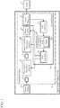
- FIG. 1 is a configuration diagram illustrating a signal amplification device including an impedance tuner according to the first embodiment of the present invention.
- a signal source 1 is an amplifier such as a traveling wave tube amplifier (TWTA) or a solid state power amplifier (SSPA), for example, and outputs an amplified signal to the impedance tuner 2.
- TWTA traveling wave tube amplifier
- SSPA solid state power amplifier
- the impedance tuner 2 is a device for matching the impedance of the signal source 1 and the impedance of a load 3.
- the load 3 is a load whose impedance P1 is unknown.
- a first transmission line 11 is a transmission line connected at one end thereof to the output end of the signal source 1 and having an electrical length of a quarter wavelength at the frequency of a signal output from the signal source 1.
- a first variable reactance element 12 is a variable reactance element connected at one end thereof to the other end of the first transmission line 11.
- a second transmission line 13 is a transmission line connected at one end thereof to the other end of the first variable reactance element 12 and having an electrical length of a quarter wavelength at the frequency of a signal output from the signal source 1.
- a second variable reactance element 14 is a variable reactance element connected at one end thereof to the other end of the second transmission line 13.
- a phase shifter 15 is connected at one end thereof to the other end of the second variable reactance element 14, shifts the phase of a signal having passed through the second variable reactance element 14, and outputs the phase-shifted signal.
- a control circuit 16 includes a vector detector 17, an A/D converter 18, a calculation processing unit 19, and a D/A converter 20.
- the control circuit 16 is a circuit that detects the impedance P1 of the load 3 and controls each of the reactance value L1 of the first variable reactance element 12, the reactance value L2 of the second variable reactance element 14, and the phase shift amount ⁇ of the phase shifter 15 on the basis of the impedance P1.
- the vector detector 17 detects the impedance P1 of the load 3 and outputs a detection signal indicating the detected impedance P1 to the A/D converter 18.
- the A/D converter 18 is an analog-to-digital converter that converts the analog detection signal output from the vector detector 17 to a digital signal and outputs the digital detection signal to the calculation processing unit 19.
- the calculation processing unit 19 includes a table 19a indicating the relationship between the impedance P1 of the load 3, the reactance value L1 of the first variable reactance element 12, the reactance value L2 of the second variable reactance element 14, and the phase shift amount ⁇ of the phase shifter 15.
- the calculation processing unit 19 determines each of the reactance value L1 of the first variable reactance element 12, the reactance value L2 of the second variable reactance element 14, and the phase shift amount ⁇ of the phase shifter 15 corresponding to the impedance P1 indicated by the digital detection signal output from the A/D converter 18.
- the calculation processing unit 19 outputs, to the D/A converter 20, a control signal C1 indicating the determined reactance value L1 and a control signal C2 indicating the reactance value L2.
- the calculation processing unit 19 also outputs, to the phase shifter 15, a control signal C3 indicating the determined phase shift amount ⁇ .
- the D/A converter 20 is a digital-to-analog converter that converts the digital control signals C1 and C2 output from the calculation processing unit 19 to analog signals.
- the D/A converter 20 outputs the analog control signal C1 to the first variable reactance element 12 and outputs the analog control signal C2 to the second variable reactance element 14.
- FIG. 2 is an explanatory diagram illustrating the operation principle of the impedance tuner 2 in FIG. 1 .
- the vector detector 17 of the control circuit 16 detects the impedance P1 of the load 3 and outputs a detection signal indicating the detected impedance P1 to the A/D converter 18.
- the impedance P1 of the load is present on the constant reflection coefficient circle R1.
- the size of the constant reflection coefficient circle R1 varies depending on the impedance P1 of the load detected by the vector detector 17.
- the A/D converter 18 of the control circuit 16 converts the analog detection signal output from the vector detector 17 to a digital signal, and outputs the digital detection signal to the calculation processing unit 19.
- the calculation processing unit 19 of the control circuit 16 includes the table 19a indicating the relationship between the impedance P1 of the load 3, the reactance value L1 of the first variable reactance element 12, the reactance value L2 of the second variable reactance element 14, and the phase shift amount ⁇ of the phase shifter 15.
- FIG. 3 is an explanatory diagram illustrating an example of the table 19a.
- the calculation processing unit 19 determines each of the reactance value L1 of the first variable reactance element 12, the reactance value L2 of the second variable reactance element 14, and the phase shift amount ⁇ of the phase shifter 15 corresponding to the impedance P1 indicated by the digital detection signal output from the A/D converter 18.
- L1 a is selected as the reactance value L1 of the first variable reactance element 12
- L2 a is selected as the reactance value L2 of the second variable reactance element 14
- ⁇ a is selected as the phase shift amount ⁇ of the phase shifter 15.
- L1b is selected as the reactance value L1 of the first variable reactance element 12
- L2 b is selected as the reactance value L2 of the second variable reactance element 14
- ⁇ b is selected as the phase shift amount ⁇ of the phase shifter 15.
- the calculation processing unit 19 outputs, to the D/A converter 20, the control signal C1 indicating the determined reactance value L1 and the control signal C2 indicating the reactance value L2.
- the calculation processing unit 19 also outputs, to the phase shifter 15, the control signal C3 indicating the determined phase shift amount ⁇ .
- the D/A converter 20 of the control circuit 16 converts the digital control signals C1 and C2 output from the calculation processing unit 19 to analog signals.
- the D/A converter 20 outputs the analog control signal C1 to the first variable reactance element 12 and outputs the analog control signal C2 to the second variable reactance element 14.
- the phase shifter 15 shifts the phase of a signal having passed through the second variable reactance element 14 by the phase shift amount ⁇ indicated by the control signal C3 output from the calculation processing unit 19.
- phase shifter 15 performs discrete phase shift control
- the impedance is put in the phase range of a region P5 after the phase shifter 15 performs phase shift control.
- the impedance P1 of the load 3 is moved into the region P5 having a certain phase range as illustrated in FIG. 2 .
- the table 19a of the calculation processing unit 19 stores, for each impedance P1 of the load 3, the phase shift amount ⁇ that causes the impedance to enter the region P5 after the phase shifter 15 performs phase shift control.
- the impedance enters the phase range of the region P5 after the phase shifter 15 performs phase shift control. Therefore, for example, if the impedance P1 of the load 3 is P1 a , about 110 degrees is stored in the table 19a as the phase shift amount ⁇ a corresponding to the impedance P1 a .
- an end with the smallest phase angle is the intersection of the constant conductance circle R2 passing through the point P3 having 50 ⁇ in the Smith chart and the constant reflection coefficient circle R1 or a point with a larger phase angle than the intersection of the constant conductance circle R2 and the constant reflection coefficient circle R1.
- the end with the largest phase angle (the lower end of the region P5 in the drawing) is a point with a smaller phase angle than the intersection of the constant reflection coefficient circle R1 and the real axis of the Smith chart.
- the region P5 if the phase angle of the upper end of the region P5 is ⁇ P5min [°], the region P5 has a phase range of ⁇ P5min [°] to 180[°].
- the reactance value L2 of the second variable reactance element 14 is set to the reactance value indicated by the control signal C2 output from the D/A converter 20 of the control circuit 16.
- the second variable reactance element 14 transforms the impedance using the reactance value L2 set by the control circuit 16.
- the reactance value L2 is a reactance value that causes the impedance to enter a region P6 after the second variable reactance element 14 performs impedance transformation.
- the table 19a of the calculation processing unit 19 stores, for each impedance P1 of the load 3, the reactance value L2 that causes the impedance to enter the region P6 after the second variable reactance element 14 performs impedance transformation.
- the impedance at the lower end of the region P5 is transformed to the impedance at the upper end of the region P6, and the impedance at the upper end of the region P5 is transformed to the impedance at the lower end of the region P6.
- the impedance at any point included in the region P5 is transformed to the impedance at the corresponding point in the region P6.
- the second transmission line 13 having an electrical length of a quarter wavelength at the frequency of a signal output from the signal source 1 transforms the impedance.
- the impedance in the region P6 is transformed to enter the region P7 as illustrated in FIG. 2 .
- the reactance value L1 of the first variable reactance element 12 is set to the reactance value indicated by the control signal C1 output from the D/A converter 20 of the control circuit 16.
- the first variable reactance element 12 transforms the impedance using the reactance value L1 set by the control circuit 16.
- the reactance value L1 is a reactance value that causes the impedance to be transformed to a point P8 on the real axis of the Smith chart after the first variable reactance element 12 performs impedance transformation as illustrated in FIG. 2 .
- the table 19a of the calculation processing unit 19 stores, for each impedance P1 of the load 3, the reactance value L1 that brings the impedance to the point P8 on the real axis of the Smith chart after the first variable reactance element 12 performs impedance transformation.
- the first transmission line 11 having an electrical length of a quarter wavelength at the frequency of a signal output from the signal source 1 transforms the impedance.
- the impedance at the point P8 is transformed to the point P3 having 50 ⁇ as illustrated in FIG. 2 .
- the point P8 having the impedance after the first variable reactance element 12 performs impedance transformation is uniquely determined by the region P5, which is the phase range having the impedance after the phase shifter 15 performs phase shift control.
- the point P8 is uniquely determined by the phase angle of the lower end of the region P5.
- a transmission line having the same characteristic impedance as the impedance at the point P8 is used as the second transmission line 13, and the line width of the second transmission line 13 can be uniquely determined if the region P5 is defined in advance.
- the second transmission line 13 can be used regardless of the impedance P1 of the load 3.
- the characteristic impedance of the first transmission line 11 is uniquely determined by the impedance at the point P8.
- the characteristic impedance of the first transmission line 11 is the geometric mean value of the impedance at the point P8 and the impedance at the point P3.
- control circuit 16 is configured to detect the impedance P1 of the load 3 and control each of the reactance value L1 of the first variable reactance element 12, the reactance value L2 of the second variable reactance element 14, and the phase shift amount ⁇ of the phase shifter 15 on the basis of the detected impedance P1, which is effective in achieving impedance matching even with the phase shifter 15 that performs discrete phase shift control.
- phase shifter 15 does not need to shift the phase of the impedance P1 of the load 3 to one specific point, but only needs to cause the impedance P1 to enter the region P5 having a certain phase range, so that impedance mismatch due to the control accuracy of the phase shifter 15 can be resolved.
- each of the first variable reactance element 12 and the second variable reactance element 14 may be a variable capacitor as illustrated in FIG. 4 .
- FIG. 4 is a configuration diagram illustrating a signal amplification device including another impedance tuner according to the first embodiment of the present invention.
- variable capacitor 21 is used as the first variable reactance element 12
- variable capacitor 22 is used as the second variable reactance element 14.
- Varactor diodes can be used as the variable capacitors 21 and 22.
- the table 19a of the calculation processing unit 19 stores the capacitance value of the variable capacitor 21 as the reactance value L1 of the first variable reactance element 12 and stores the capacitance value of the variable capacitor 22 as the reactance value L2 of the second variable reactance element 14.
- phase shifter 30 provided in an impedance tuner
- FIG. 5 is a configuration diagram illustrating the phase shifter 30 of the impedance tuner according to the second embodiment of the present invention.
- reference signs identical to those in FIGS. 1 and 4 designate identical or corresponding components, and the descriptions thereof are omitted.
- the phase shifter 30 shifts the phase of a signal having passed through the second variable reactance element 14 and outputs the phase-shifted signal.
- the phase shifter 30 includes transmission lines 31 to 40 that are connectable in series and switches 41 to 50 that select transmission lines to be connected in series from among the transmission lines 31 to 40.
- the control circuit 16 controls the phase shift amount ⁇ of the phase shifter 30 by controlling the selection of transmission lines at the switches 41 to 50.
- the transmission lines 31 to 35 are transmission lines having an electrical length of a half wavelength at the frequency of a signal output from the signal source 1.
- the transmission line 36 is a transmission line having an electrical length of 1/64 wavelength at the frequency of a signal output from the signal source 1.
- the transmission line 37 is a transmission line having an electrical length of 1/32 wavelength at the frequency of a signal output from the signal source 1.
- the transmission line 38 is a transmission line having an electrical length of 1/16 wavelength at the frequency of a signal output from the signal source 1.
- the transmission line 39 is a transmission line having an electrical length of 1/8 wavelength at the frequency of a signal output from the signal source 1.
- the transmission line 40 is a transmission line having an electrical length of a quarter wavelength at the frequency of a signal output from the signal source 1.
- the switches 41 and 42 are changeover switches for selecting either the transmission line 31 or the transmission line 36.
- the switches 43 and 44 are changeover switches for selecting either the transmission line 32 or the transmission line 37.
- the switches 45 and 46 are changeover switches for selecting either the transmission line 33 or the transmission line 38.
- the switches 47 and 48 are changeover switches for selecting either the transmission line 34 or the transmission line 39.
- the switches 49 and 50 are changeover switches for selecting either the transmission line 35 or the transmission line 40.
- the calculation processing unit 19 of the control circuit 16 determines the phase shift amount ⁇ of the phase shifter 30 and outputs the control signal C3 indicating the determined phase shift amount ⁇ to the phase shifter 30.
- the switches 41 to 50 of the phase shifter 30 set the phase shift amount ⁇ of the phase shifter 30 by selecting transmission lines on the basis of the phase shift amount ⁇ indicated by the control signal C3 output from the calculation processing unit 19.
- phase shifter 30 in which the phase shift amount ⁇ is represented by five bits is illustrated, but this is only one example, and the number of bits representing the phase shift amount ⁇ can be increased or reduced by changing the number of transmission lines included in the phase shifter 30.
- the present invention is suitable for an impedance tuner and a signal amplification device including variable reactance elements and a phase shifter.
Landscapes
- Engineering & Computer Science (AREA)
- Power Engineering (AREA)
- Amplifiers (AREA)
- Networks Using Active Elements (AREA)
- Waveguide Switches, Polarizers, And Phase Shifters (AREA)
- Transmitters (AREA)
Abstract
Description
- The present invention relates to an impedance tuner and a signal amplification device including variable reactance elements and a phase shifter.
- Mechanically controlled impedance tuners are capable of matching the impedance of a signal source and the impedance of a load by driving a slug in a waveguide using a motor.
- Mechanically controlled impedance tuners need a lot of time to completely drive the slug.
- Patent Literature 1 below discloses an electronically controlled impedance tuner as a compact impedance tuner that operates faster than mechanically controlled impedance tuners.
- The impedance tuner disclosed in Patent Literature 1 includes a variable reactance element and a phase shifter.
- The phase shifter of the impedance tuner controls the phase of a signal from a signal source to a load connected to the impedance tuner in a manner as to move the impedance of the load to a point on a constant conductance circle passing through the 50 Ω point of the Smith chart.
- The variable reactance element of the impedance tuner achieves impedance matching by transforming the impedance at the point on the constant conductance circle to 50 Ω.
- Patent Literature 1:
JP 2003-318689 A - Since the conventional impedance tuner is configured as described above, if the phase shifter can accurately move the impedance of the load to a point on the constant conductance circle passing through the 50 Ω point of the Smith chart, the impedance of the signal source and the impedance of the load can be matched. However, because the phase shifter performs discrete phase shift control in principle, the impedance might be likely to reach some point other than the point on the constant conductance circle passing through a point having 50 Ω in the Smith chart after phase shift control. There is a problem in that the accuracy of matching between the impedance of the signal source and the impedance of the load is degraded.
-
FIG. 6 is an explanatory diagram illustrating a state in which the impedance of a signal source and the impedance of a load are sufficiently matched. - In the example of
FIG. 6 , the impedance P1 of the load is present on a constant reflection coefficient circle R1. - By controlling the phase of a signal output from the signal source to the load, the phase shifter moves the impedance P1 of the load to a point P2 on a constant conductance circle R2 passing through a point P3 having 50 Ω in the Smith chart.
- The variable reactance element transforms the impedance at the point P2 on the constant conductance circle R2 to the point P3.
-
FIG. 7 is an explanatory diagram illustrating a state in which the accuracy of matching between the impedance of a signal source and the impedance of a load is degraded. - Because the phase shifter performs discrete phase shift control in principle, the impedance might reach a point P4 within some phase range, which is shifted to the point P2 on the constant conductance circle R2 after the phase shifter performs phase shift control.
- When the variable reactance element transforms the impedance that is shifted to the point P2, a mismatch occurs by the range of R3.
- The present invention has been made to solve the above problems, and an object thereof is to obtain an impedance tuner and a signal amplification device capable of achieving impedance matching even with a phase shifter that performs discrete phase shift control.
- An impedance tuner according to the present invention includes: a first transmission line connected at one end to an output end of a signal source and having an electrical length of a quarter wavelength at a frequency of a signal output from the signal source; a first variable reactance element connected at one end to another end of the first transmission line; a second transmission line connected at one end to another end of the first variable reactance element and having an electrical length of a quarter wavelength at the frequency of the signal; a second variable reactance element connected at one end to another end of the second transmission line; and a phase shifter connected at one end to another end of the second variable reactance element for shifting a phase of the signal and outputting a phase-shifted signal to a load, and a control circuit detects an impedance of the load and controls each of reactance values of the first and second variable reactance elements and a phase shift amount of the phase shifter on the basis of the detected impedance.
- According to the present invention, because the control circuit is configured to detect the impedance of the load and control each of the reactance values of the first and second variable reactance elements and the phase shift amount of the phase shifter on the basis of the detected impedance, the present invention is effective in achieving impedance matching even with the phase shifter that performs discrete phase shift control.
-
-
FIG. 1 is a configuration diagram illustrating a signal amplification device including an impedance tuner according to a first embodiment of the present invention. -
FIG. 2 is an explanatory diagram illustrating the operation principle of theimpedance tuner 2 inFIG. 1 . -
FIG. 3 is an explanatory diagram illustrating an example of a table 19a. -
FIG. 4 is a configuration diagram illustrating a signal amplification device including another impedance tuner according to the first embodiment of the present invention. -
FIG. 5 is a configuration diagram illustrating aphase shifter 30 of an impedance tuner according to a second embodiment of the present invention. -
FIG. 6 is an explanatory diagram illustrating a state in which the impedance of a signal source and the impedance of a load are sufficiently matched. -
FIG. 7 is an explanatory diagram illustrating a state in which the accuracy of matching between the impedance of a signal source and the impedance of a load is degraded. - Hereinafter, in order to explain the present invention in more detail, embodiments for carrying out the present invention will be described with reference to the accompanying drawings.
-
FIG. 1 is a configuration diagram illustrating a signal amplification device including an impedance tuner according to the first embodiment of the present invention. - In
FIG. 1 , a signal source 1 is an amplifier such as a traveling wave tube amplifier (TWTA) or a solid state power amplifier (SSPA), for example, and outputs an amplified signal to theimpedance tuner 2. - The
impedance tuner 2 is a device for matching the impedance of the signal source 1 and the impedance of a load 3. - The load 3 is a load whose impedance P1 is unknown.
- A
first transmission line 11 is a transmission line connected at one end thereof to the output end of the signal source 1 and having an electrical length of a quarter wavelength at the frequency of a signal output from the signal source 1. - A first
variable reactance element 12 is a variable reactance element connected at one end thereof to the other end of thefirst transmission line 11. - A
second transmission line 13 is a transmission line connected at one end thereof to the other end of the firstvariable reactance element 12 and having an electrical length of a quarter wavelength at the frequency of a signal output from the signal source 1. - A second
variable reactance element 14 is a variable reactance element connected at one end thereof to the other end of thesecond transmission line 13. - A
phase shifter 15 is connected at one end thereof to the other end of the secondvariable reactance element 14, shifts the phase of a signal having passed through the secondvariable reactance element 14, and outputs the phase-shifted signal. - A
control circuit 16 includes avector detector 17, an A/D converter 18, acalculation processing unit 19, and a D/A converter 20. - The
control circuit 16 is a circuit that detects the impedance P1 of the load 3 and controls each of the reactance value L1 of the firstvariable reactance element 12, the reactance value L2 of the secondvariable reactance element 14, and the phase shift amount ϕ of thephase shifter 15 on the basis of the impedance P1. - The
vector detector 17 detects the impedance P1 of the load 3 and outputs a detection signal indicating the detected impedance P1 to the A/D converter 18. - The A/
D converter 18 is an analog-to-digital converter that converts the analog detection signal output from thevector detector 17 to a digital signal and outputs the digital detection signal to thecalculation processing unit 19. - The
calculation processing unit 19 includes a table 19a indicating the relationship between the impedance P1 of the load 3, the reactance value L1 of the firstvariable reactance element 12, the reactance value L2 of the secondvariable reactance element 14, and the phase shift amount ϕ of thephase shifter 15. - With reference to the table 19a, the
calculation processing unit 19 determines each of the reactance value L1 of the firstvariable reactance element 12, the reactance value L2 of the secondvariable reactance element 14, and the phase shift amount ϕ of thephase shifter 15 corresponding to the impedance P1 indicated by the digital detection signal output from the A/D converter 18. - The
calculation processing unit 19 outputs, to the D/A converter 20, a control signal C1 indicating the determined reactance value L1 and a control signal C2 indicating the reactance value L2. - The
calculation processing unit 19 also outputs, to thephase shifter 15, a control signal C3 indicating the determined phase shift amount ϕ. - The D/
A converter 20 is a digital-to-analog converter that converts the digital control signals C1 and C2 output from thecalculation processing unit 19 to analog signals. - The D/
A converter 20 outputs the analog control signal C1 to the firstvariable reactance element 12 and outputs the analog control signal C2 to the secondvariable reactance element 14. - Next, the operation will be described.
-
FIG. 2 is an explanatory diagram illustrating the operation principle of theimpedance tuner 2 inFIG. 1 . - The
vector detector 17 of thecontrol circuit 16 detects the impedance P1 of the load 3 and outputs a detection signal indicating the detected impedance P1 to the A/D converter 18. - In the example of
FIG. 2 , the impedance P1 of the load is present on the constant reflection coefficient circle R1. The size of the constant reflection coefficient circle R1 varies depending on the impedance P1 of the load detected by thevector detector 17. - The A/
D converter 18 of thecontrol circuit 16 converts the analog detection signal output from thevector detector 17 to a digital signal, and outputs the digital detection signal to thecalculation processing unit 19. - The
calculation processing unit 19 of thecontrol circuit 16 includes the table 19a indicating the relationship between the impedance P1 of the load 3, the reactance value L1 of the firstvariable reactance element 12, the reactance value L2 of the secondvariable reactance element 14, and the phase shift amount ϕ of thephase shifter 15. -
FIG. 3 is an explanatory diagram illustrating an example of the table 19a. - With reference to the table 19a, the
calculation processing unit 19 determines each of the reactance value L1 of the firstvariable reactance element 12, the reactance value L2 of the secondvariable reactance element 14, and the phase shift amount ϕ of thephase shifter 15 corresponding to the impedance P1 indicated by the digital detection signal output from the A/D converter 18. - In the example of
FIG. 3 , if the impedance P1 of the load 3 is P1a, L1a is selected as the reactance value L1 of the firstvariable reactance element 12, L2a is selected as the reactance value L2 of the secondvariable reactance element 14, and ϕa is selected as the phase shift amount ϕ of thephase shifter 15. - If the impedance P1 of the load 3 is P1b, L1b is selected as the reactance value L1 of the first
variable reactance element 12, L2b is selected as the reactance value L2 of the secondvariable reactance element 14, and ϕb is selected as the phase shift amount ϕ of thephase shifter 15. - The
calculation processing unit 19 outputs, to the D/A converter 20, the control signal C1 indicating the determined reactance value L1 and the control signal C2 indicating the reactance value L2. - The
calculation processing unit 19 also outputs, to thephase shifter 15, the control signal C3 indicating the determined phase shift amount ϕ. - The D/
A converter 20 of thecontrol circuit 16 converts the digital control signals C1 and C2 output from thecalculation processing unit 19 to analog signals. - The D/
A converter 20 outputs the analog control signal C1 to the firstvariable reactance element 12 and outputs the analog control signal C2 to the secondvariable reactance element 14. - The
phase shifter 15 shifts the phase of a signal having passed through the secondvariable reactance element 14 by the phase shift amount ϕ indicated by the control signal C3 output from thecalculation processing unit 19. - Because the
phase shifter 15 performs discrete phase shift control, the impedance is put in the phase range of a region P5 after thephase shifter 15 performs phase shift control. - Therefore, the impedance P1 of the load 3 is moved into the region P5 having a certain phase range as illustrated in
FIG. 2 . - Note that the table 19a of the
calculation processing unit 19 stores, for each impedance P1 of the load 3, the phase shift amount ϕ that causes the impedance to enter the region P5 after thephase shifter 15 performs phase shift control. - In the example of
FIG. 2 , if the phase shift amount ϕ is about 110 degrees, the impedance enters the phase range of the region P5 after thephase shifter 15 performs phase shift control. Therefore, for example, if the impedance P1 of the load 3 is P1a, about 110 degrees is stored in the table 19a as the phase shift amount ϕa corresponding to the impedance P1a. - Here, in the region P5, an end with the smallest phase angle (the upper end of the region P5 in the drawing) is the intersection of the constant conductance circle R2 passing through the point P3 having 50 Ω in the Smith chart and the constant reflection coefficient circle R1 or a point with a larger phase angle than the intersection of the constant conductance circle R2 and the constant reflection coefficient circle R1.
- In the region P5, the end with the largest phase angle (the lower end of the region P5 in the drawing) is a point with a smaller phase angle than the intersection of the constant reflection coefficient circle R1 and the real axis of the Smith chart.
- Therefore, in the region P5, if the phase angle of the upper end of the region P5 is θP5min[°], the region P5 has a phase range of θP5min[°] to 180[°].
- The reactance value L2 of the second
variable reactance element 14 is set to the reactance value indicated by the control signal C2 output from the D/A converter 20 of thecontrol circuit 16. - After the
phase shifter 15 performs phase shift control, the secondvariable reactance element 14 transforms the impedance using the reactance value L2 set by thecontrol circuit 16. - The reactance value L2 is a reactance value that causes the impedance to enter a region P6 after the second
variable reactance element 14 performs impedance transformation. - Therefore, the table 19a of the
calculation processing unit 19 stores, for each impedance P1 of the load 3, the reactance value L2 that causes the impedance to enter the region P6 after the secondvariable reactance element 14 performs impedance transformation. - As illustrated in
FIG. 2 , the impedance at the lower end of the region P5 is transformed to the impedance at the upper end of the region P6, and the impedance at the upper end of the region P5 is transformed to the impedance at the lower end of the region P6. - Therefore, the impedance at any point included in the region P5 is transformed to the impedance at the corresponding point in the region P6.
- After the second
variable reactance element 14 performs impedance transformation, thesecond transmission line 13 having an electrical length of a quarter wavelength at the frequency of a signal output from the signal source 1 transforms the impedance. - Consequently, the impedance in the region P6 is transformed to enter the region P7 as illustrated in
FIG. 2 . - The reactance value L1 of the first
variable reactance element 12 is set to the reactance value indicated by the control signal C1 output from the D/A converter 20 of thecontrol circuit 16. - After the
second transmission line 13 performs impedance transformation, the firstvariable reactance element 12 transforms the impedance using the reactance value L1 set by thecontrol circuit 16. - The reactance value L1 is a reactance value that causes the impedance to be transformed to a point P8 on the real axis of the Smith chart after the first
variable reactance element 12 performs impedance transformation as illustrated inFIG. 2 . - Therefore, the table 19a of the
calculation processing unit 19 stores, for each impedance P1 of the load 3, the reactance value L1 that brings the impedance to the point P8 on the real axis of the Smith chart after the firstvariable reactance element 12 performs impedance transformation. - After the first
variable reactance element 12 performs impedance transformation, thefirst transmission line 11 having an electrical length of a quarter wavelength at the frequency of a signal output from the signal source 1 transforms the impedance. - Consequently, the impedance at the point P8 is transformed to the point P3 having 50 Ω as illustrated in
FIG. 2 . - The point P8, having the impedance after the first
variable reactance element 12 performs impedance transformation, is uniquely determined by the region P5, which is the phase range having the impedance after thephase shifter 15 performs phase shift control. In particular, the point P8 is uniquely determined by the phase angle of the lower end of the region P5. - Therefore, a transmission line having the same characteristic impedance as the impedance at the point P8 is used as the
second transmission line 13, and the line width of thesecond transmission line 13 can be uniquely determined if the region P5 is defined in advance. Thesecond transmission line 13 can be used regardless of the impedance P1 of the load 3. - Since the
first transmission line 11 has the function of transforming the impedance at the point P8 to the impedance at the point P3, the characteristic impedance of thefirst transmission line 11 is uniquely determined by the impedance at the point P8. - Specifically, the characteristic impedance of the
first transmission line 11 is the geometric mean value of the impedance at the point P8 and the impedance at the point P3. - As apparent from the above description, according to the first embodiment, because the
control circuit 16 is configured to detect the impedance P1 of the load 3 and control each of the reactance value L1 of the firstvariable reactance element 12, the reactance value L2 of the secondvariable reactance element 14, and the phase shift amount ϕ of thephase shifter 15 on the basis of the detected impedance P1, which is effective in achieving impedance matching even with thephase shifter 15 that performs discrete phase shift control. - That is, the
phase shifter 15 does not need to shift the phase of the impedance P1 of the load 3 to one specific point, but only needs to cause the impedance P1 to enter the region P5 having a certain phase range, so that impedance mismatch due to the control accuracy of thephase shifter 15 can be resolved. - Although the impedance tuner includes the first
variable reactance element 12 and the secondvariable reactance element 14 in the example described in the first embodiment, each of the firstvariable reactance element 12 and the secondvariable reactance element 14 may be a variable capacitor as illustrated inFIG. 4 . -
FIG. 4 is a configuration diagram illustrating a signal amplification device including another impedance tuner according to the first embodiment of the present invention. - In
FIG. 4 , avariable capacitor 21 is used as the firstvariable reactance element 12, and avariable capacitor 22 is used as the secondvariable reactance element 14. - Varactor diodes can be used as the
variable capacitors - In the example of
FIG. 4 , the table 19a of thecalculation processing unit 19 stores the capacitance value of thevariable capacitor 21 as the reactance value L1 of the firstvariable reactance element 12 and stores the capacitance value of thevariable capacitor 22 as the reactance value L2 of the secondvariable reactance element 14. - In the second embodiment, a specific configuration example of a
phase shifter 30 provided in an impedance tuner will be described. -
FIG. 5 is a configuration diagram illustrating thephase shifter 30 of the impedance tuner according to the second embodiment of the present invention. InFIG. 5 , reference signs identical to those inFIGS. 1 and4 designate identical or corresponding components, and the descriptions thereof are omitted. - In the same manner as the
phase shifter 15 in the first embodiment above, thephase shifter 30 shifts the phase of a signal having passed through the secondvariable reactance element 14 and outputs the phase-shifted signal. - The
phase shifter 30 includestransmission lines 31 to 40 that are connectable in series and switches 41 to 50 that select transmission lines to be connected in series from among thetransmission lines 31 to 40. - The
control circuit 16 controls the phase shift amount ϕ of thephase shifter 30 by controlling the selection of transmission lines at theswitches 41 to 50. - The
transmission lines 31 to 35 are transmission lines having an electrical length of a half wavelength at the frequency of a signal output from the signal source 1. - The
transmission line 36 is a transmission line having an electrical length of 1/64 wavelength at the frequency of a signal output from the signal source 1. - The
transmission line 37 is a transmission line having an electrical length of 1/32 wavelength at the frequency of a signal output from the signal source 1. - The
transmission line 38 is a transmission line having an electrical length of 1/16 wavelength at the frequency of a signal output from the signal source 1. - The
transmission line 39 is a transmission line having an electrical length of 1/8 wavelength at the frequency of a signal output from the signal source 1. - The
transmission line 40 is a transmission line having an electrical length of a quarter wavelength at the frequency of a signal output from the signal source 1. - The
switches transmission line 31 or thetransmission line 36. - The
switches 43 and 44 are changeover switches for selecting either the transmission line 32 or thetransmission line 37. - The
switches transmission line 33 or thetransmission line 38. - The
switches transmission line 34 or thetransmission line 39. - The
switches transmission line 35 or thetransmission line 40. - Next, the operation will be described.
- As in the first embodiment above, the
calculation processing unit 19 of thecontrol circuit 16 determines the phase shift amount ϕ of thephase shifter 30 and outputs the control signal C3 indicating the determined phase shift amount ϕ to thephase shifter 30. - The
switches 41 to 50 of thephase shifter 30 set the phase shift amount ϕ of thephase shifter 30 by selecting transmission lines on the basis of the phase shift amount ϕ indicated by the control signal C3 output from thecalculation processing unit 19. - In
FIG. 5 , the example of thephase shifter 30 in which the phase shift amount ϕ is represented by five bits is illustrated, but this is only one example, and the number of bits representing the phase shift amount ϕ can be increased or reduced by changing the number of transmission lines included in thephase shifter 30. - Note that the present invention allows within the scope thereof any combination of embodiments, modification of any component in each embodiment, or removal of any component from each embodiment.
- The present invention is suitable for an impedance tuner and a signal amplification device including variable reactance elements and a phase shifter.
-
- 1
- signal source
- 2
- impedance tuner
- 3
- load
- 11
- first transmission line
- 12
- first variable reactance element
- 13
- second transmission line
- 14
- second variable reactance element
- 15
- phase shifter
- 16
- control circuit
- 17
- vector detector
- 18
- A/D converter
- 19
- calculation processing unit
- 20
- D/A converter
- 21, 22
- variable capacitor
- 30
- phase shifter
- 31 to 40
- transmission line
- 41 to 50
- switch
Claims (6)
- An impedance tuner comprising:a first transmission line connected at one end thereof to an output end of a signal source and having an electrical length of a quarter wavelength at a frequency of a signal output from the signal source;a first variable reactance element connected at one end thereof to another end of the first transmission line;a second transmission line connected at one end thereof to another end of the first variable reactance element and having an electrical length of a quarter wavelength at the frequency of the signal;a second variable reactance element connected at one end thereof to another end of the second transmission line;a phase shifter, connected at one end thereof to another end of the second variable reactance element, for shifting a phase of the signal and outputting a phase-shifted signal to a load; anda control circuit for detecting an impedance of the load and controlling each of reactance values of the first and second variable reactance elements and a phase shift amount of the phase shifter on a basis of the impedance.
- The impedance tuner according to claim 1,
wherein the control circuit includes a table indicating a relationship between the impedance of the load, and the reactance values of the first and second variable reactance elements, and the phase shift amount of the phase shifter, and determines, with reference to the table, each of the reactance values of the first and second variable reactance elements and the phase shift amount of the phase shifter corresponding to the impedance of the load. - The impedance tuner according to claim 1,
wherein the control circuit controls each of the reactance values of the first and second variable reactance elements and the phase shift amount of the phase shifter in a manner as to cause the output end of the signal source to have 50 ohms. - The impedance tuner according to claim 1,
wherein a varactor diode is used as the first and second variable reactance elements. - The impedance tuner according to claim 1,
wherein the phase shifter includes:a plurality of transmission lines connectable in series; anda plurality of switches for selecting transmission lines to be connected in series from among the plurality of transmission lines, andthe control circuit controls the phase shift amount of the phase shifter by controlling selection of transmission lines at the plurality of switches. - A signal amplification device comprising:an amplifier for amplifying a signal;a first transmission line connected at one end thereof to an output end of the amplifier and having an electrical length of a quarter wavelength at a frequency of a signal output from the amplifier;a first variable reactance element connected at one end thereof to another end of the first transmission line;a second transmission line connected at one end thereof to another end of the first variable reactance element and having an electrical length of a quarter wavelength at the frequency of the signal;a second variable reactance element connected at one end thereof to another end of the second transmission line;a phase shifter, connected at one end thereof to another end of the second variable reactance element, for shifting a phase of the signal and outputting a phase-shifted signal to a load; anda control circuit for detecting an impedance of the load and controlling each of reactance values of the first and second variable reactance elements and a phase shift amount of the phase shifter on a basis of the impedance.
Applications Claiming Priority (1)
| Application Number | Priority Date | Filing Date | Title |
|---|---|---|---|
| PCT/JP2017/019372 WO2018216140A1 (en) | 2017-05-24 | 2017-05-24 | Impedance tuner and signal amplification device |
Publications (2)
| Publication Number | Publication Date |
|---|---|
| EP3618275A1 true EP3618275A1 (en) | 2020-03-04 |
| EP3618275A4 EP3618275A4 (en) | 2020-06-03 |
Family
ID=64396382
Family Applications (1)
| Application Number | Title | Priority Date | Filing Date |
|---|---|---|---|
| EP17910949.1A Withdrawn EP3618275A4 (en) | 2017-05-24 | 2017-05-24 | Impedance tuner and signal amplification device |
Country Status (4)
| Country | Link |
|---|---|
| US (1) | US11005452B2 (en) |
| EP (1) | EP3618275A4 (en) |
| JP (1) | JP6587780B2 (en) |
| WO (1) | WO2018216140A1 (en) |
Families Citing this family (2)
| Publication number | Priority date | Publication date | Assignee | Title |
|---|---|---|---|---|
| CN113347644B (en) * | 2021-05-31 | 2022-07-19 | 武汉虹信科技发展有限责任公司 | Signal phase detection method of dielectric phase shifter, dielectric phase shifter and antenna |
| CN116990732A (en) * | 2022-04-26 | 2023-11-03 | 通用电气精准医疗有限责任公司 | Impedance tuner, magnetic resonance system, transmitting device and transmitting method |
Family Cites Families (8)
| Publication number | Priority date | Publication date | Assignee | Title |
|---|---|---|---|---|
| US4321706A (en) * | 1980-07-14 | 1982-03-23 | John Fluke Mfg. Co., Inc. | Frequency modulated phase-locked loop signal source |
| JP2003318689A (en) * | 2002-04-23 | 2003-11-07 | Kanazawa Inst Of Technology | Matching circuit and reflected wave detection circuit |
| EP1730838A1 (en) * | 2004-03-31 | 2006-12-13 | Xcom Wireless, Inc. | Electronically controlled hybrid digital and analog phase shifter |
| US7646268B1 (en) * | 2006-12-22 | 2010-01-12 | Christos Tsironis | Low frequency harmonic load pull tuner and method |
| US8018277B2 (en) * | 2008-09-09 | 2011-09-13 | Quantance, Inc. | RF power amplifier system with impedance modulation |
| JP2013229832A (en) * | 2012-04-27 | 2013-11-07 | Taiyo Yuden Co Ltd | Impedance matching circuit |
| WO2014132338A1 (en) * | 2013-02-26 | 2014-09-04 | 三菱電機株式会社 | Impedance tuner and power amplifying apparatus |
| JP2015130560A (en) * | 2014-01-06 | 2015-07-16 | 株式会社村田製作所 | Antenna matching circuit and control method thereof |
-
2017
- 2017-05-24 US US16/609,847 patent/US11005452B2/en not_active Expired - Fee Related
- 2017-05-24 EP EP17910949.1A patent/EP3618275A4/en not_active Withdrawn
- 2017-05-24 WO PCT/JP2017/019372 patent/WO2018216140A1/en not_active Ceased
- 2017-05-24 JP JP2019519879A patent/JP6587780B2/en not_active Expired - Fee Related
Also Published As
| Publication number | Publication date |
|---|---|
| US11005452B2 (en) | 2021-05-11 |
| EP3618275A4 (en) | 2020-06-03 |
| WO2018216140A1 (en) | 2018-11-29 |
| JPWO2018216140A1 (en) | 2019-11-07 |
| JP6587780B2 (en) | 2019-10-09 |
| US20200076408A1 (en) | 2020-03-05 |
Similar Documents
| Publication | Publication Date | Title |
|---|---|---|
| US6297696B1 (en) | Optimized power amplifier | |
| CN102193063B (en) | Detector circuit and semiconductor device using same | |
| JP5167053B2 (en) | Automatic matching method and automatic matching circuit | |
| KR101294434B1 (en) | Impedance matching apparatus and impedance matching method | |
| GB2363925A (en) | Reduction of mobile phone transmitter amplifier distortion due to output mismatch | |
| CN105223526A (en) | A kind of radio-frequency sending coil impedance matching circuit and method | |
| US20240030874A1 (en) | Amplifier assembly and phase shifting method | |
| US20150035595A1 (en) | Low-noise receiver with complex rf attenuator | |
| EP3618275A1 (en) | Impedance tuner and signal amplification device | |
| US9692461B2 (en) | Amplifier module | |
| KR100191430B1 (en) | Automatic matching circuit device capable of frequency shifting and implementation method | |
| US20240267032A1 (en) | Phase shifter and phase shifting method | |
| KR102623717B1 (en) | Load detection circuit and amplifier circuit | |
| RU2308145C2 (en) | Antenna-matching device | |
| CN119865137B (en) | Power combining device and radio frequency power supply system | |
| FI86350C (en) | Method and apparatus for automatic gain control in the high frequency amplifier | |
| GB2158620A (en) | Power control for radio transmitters | |
| KR100598681B1 (en) | High frequency sensor of impedance matching device | |
| EP4730647A1 (en) | Receiver and phase modulator being part of the receiver and corresponding method | |
| US20040090271A1 (en) | Variable gain amplifier for high frequency band using microstrip hybrid | |
| EP4730662A1 (en) | Receiver | |
| JP4319937B2 (en) | Transmitter | |
| CN119865135A (en) | Power synthesis device and radio frequency power supply system | |
| CN119966423A (en) | RF power supply equipment and RF power supply system | |
| CN120263216A (en) | Chip and chip cascade structure, calibration method, radar device and electronic equipment |
Legal Events
| Date | Code | Title | Description |
|---|---|---|---|
| PUAI | Public reference made under article 153(3) epc to a published international application that has entered the european phase |
Free format text: ORIGINAL CODE: 0009012 |
|
| 17P | Request for examination filed |
Effective date: 20191110 |
|
| AK | Designated contracting states |
Kind code of ref document: A1 Designated state(s): AL AT BE BG CH CY CZ DE DK EE ES FI FR GB GR HR HU IE IS IT LI LT LU LV MC MK MT NL NO PL PT RO RS SE SI SK SM TR |
|
| AX | Request for extension of the european patent |
Extension state: BA ME |
|
| A4 | Supplementary search report drawn up and despatched |
Effective date: 20200506 |
|
| RIC1 | Information provided on ipc code assigned before grant |
Ipc: H03H 7/38 20060101AFI20200428BHEP Ipc: H03H 7/20 20060101ALI20200428BHEP Ipc: H03H 7/18 20060101ALI20200428BHEP |
|
| DAV | Request for validation of the european patent (deleted) | ||
| DAX | Request for extension of the european patent (deleted) | ||
| STAA | Information on the status of an ep patent application or granted ep patent |
Free format text: STATUS: THE APPLICATION HAS BEEN WITHDRAWN |
|
| 18W | Application withdrawn |
Effective date: 20201014 |