EP3618186B1 - Multi-frequency antenna system, and method for controlling different frequency interference in a multi-frequency antenna system - Google Patents
Multi-frequency antenna system, and method for controlling different frequency interference in a multi-frequency antenna system Download PDFInfo
- Publication number
- EP3618186B1 EP3618186B1 EP18809449.4A EP18809449A EP3618186B1 EP 3618186 B1 EP3618186 B1 EP 3618186B1 EP 18809449 A EP18809449 A EP 18809449A EP 3618186 B1 EP3618186 B1 EP 3618186B1
- Authority
- EP
- European Patent Office
- Prior art keywords
- feed
- differential mode
- signal
- section
- radiating element
- Prior art date
- Legal status (The legal status is an assumption and is not a legal conclusion. Google has not performed a legal analysis and makes no representation as to the accuracy of the status listed.)
- Active
Links
Images



Classifications
-
- H—ELECTRICITY
- H01—ELECTRIC ELEMENTS
- H01Q—ANTENNAS, i.e. RADIO AERIALS
- H01Q1/00—Details of, or arrangements associated with, antennas
- H01Q1/52—Means for reducing coupling between antennas; Means for reducing coupling between an antenna and another structure
- H01Q1/521—Means for reducing coupling between antennas; Means for reducing coupling between an antenna and another structure reducing the coupling between adjacent antennas
-
- H—ELECTRICITY
- H01—ELECTRIC ELEMENTS
- H01Q—ANTENNAS, i.e. RADIO AERIALS
- H01Q1/00—Details of, or arrangements associated with, antennas
- H01Q1/48—Earthing means; Earth screens; Counterpoises
-
- H—ELECTRICITY
- H01—ELECTRIC ELEMENTS
- H01Q—ANTENNAS, i.e. RADIO AERIALS
- H01Q1/00—Details of, or arrangements associated with, antennas
- H01Q1/50—Structural association of antennas with earthing switches, lead-in devices or lightning protectors
-
- H—ELECTRICITY
- H01—ELECTRIC ELEMENTS
- H01Q—ANTENNAS, i.e. RADIO AERIALS
- H01Q5/00—Arrangements for simultaneous operation of antennas on two or more different wavebands, e.g. dual-band or multi-band arrangements
- H01Q5/10—Resonant antennas
-
- H—ELECTRICITY
- H01—ELECTRIC ELEMENTS
- H01Q—ANTENNAS, i.e. RADIO AERIALS
- H01Q5/00—Arrangements for simultaneous operation of antennas on two or more different wavebands, e.g. dual-band or multi-band arrangements
- H01Q5/30—Arrangements for providing operation on different wavebands
- H01Q5/307—Individual or coupled radiating elements, each element being fed in an unspecified way
-
- H—ELECTRICITY
- H01—ELECTRIC ELEMENTS
- H01Q—ANTENNAS, i.e. RADIO AERIALS
- H01Q5/00—Arrangements for simultaneous operation of antennas on two or more different wavebands, e.g. dual-band or multi-band arrangements
- H01Q5/50—Feeding or matching arrangements for broad-band or multi-band operation
-
- H—ELECTRICITY
- H01—ELECTRIC ELEMENTS
- H01Q—ANTENNAS, i.e. RADIO AERIALS
- H01Q15/00—Devices for reflection, refraction, diffraction or polarisation of waves radiated from an antenna, e.g. quasi-optical devices
- H01Q15/14—Reflecting surfaces; Equivalent structures
-
- H—ELECTRICITY
- H01—ELECTRIC ELEMENTS
- H01Q—ANTENNAS, i.e. RADIO AERIALS
- H01Q21/00—Antenna arrays or systems
- H01Q21/24—Combinations of antenna units polarised in different directions for transmitting or receiving circularly and elliptically polarised waves or waves linearly polarised in any direction
- H01Q21/26—Turnstile or like antennas comprising arrangements of three or more elongated elements disposed radially and symmetrically in a horizontal plane about a common centre
Definitions
- the balun further includes a transport layer of a feed signal
- the conductive structure includes a short-circuit stub and a microstrip
- the microstrip is electrically connected to the grounding structure.
- the transferring the differential mode signal to the grounding structure by using the at least one conductive structure includes:
- a short-circuit stub may be introduced into a feed structure of the high-band radiating element, to divert a sensed differential mode signal to the grounding apparatus.
- a plated through hole is introduced into the feed structure of the high-band radiating element, to directly connect to a transport layer of a feed signal and the signal ground layer, so that the differential mode signal flows from a feed point to the microstrip, and finally flows from the microstrip to the grounding apparatus.
- differential mode radiation cannot be excited between the radiation arms of the high-band radiating element. Consequently, intensity of parasitic resonance generated in a low-band radiating element that has a relatively low operating frequency band decreases, and finally an antenna array of the low-band radiating element can operate normally.
- FIG. 6c is a schematic structural diagram when the short-circuit stub is disposed on the coupling section.
- the differential mode signal flows from the feed section into the microstrip.
- the short-circuit stub may also be separately disposed on at least one of the transmission section, the feed section, or the coupling section.
- FIG. 7a the short-circuit stub is disposed on the transmission section of the transport layer of the feed signal.
- FIG. 7b the short-circuit stub is disposed on the feed section of the transport layer of the feed signal.
- FIG. 7c the short-circuit stub is disposed on the coupling section of the transport layer of the feed signal.
- the disclosed system, apparatus, and method may be implemented in other manners.
- the described apparatus embodiment is merely an example.
- the module division is merely logical function division and may be other division during actual implementation.
- a plurality of modules or components may be combined or integrated into another system, or some features may be ignored or not performed.
- the displayed or discussed mutual couplings or direct couplings or communication connections may be implemented through some interfaces.
- the indirect couplings or communication connections between the apparatuses or modules may be implemented in electronic, mechanical, or other forms.
- modules described as separate parts may or may not be physically separate, and parts displayed as modules may or may not be physical modules, may be located in one position, or may be distributed on a plurality of network modules. Some or all the modules may be selected based on an actual requirement to achieve the objectives of the solutions of the embodiments.
- the computer program product includes one or more computer instructions.
- the computer may be a general-purpose computer, a dedicated computer, a computer network, or another programmable apparatus.
- the computer instructions may be stored in a computer-readable storage medium or may be transmitted from one computer-readable storage medium to another computer-readable storage medium.
- the computer instruction may be transmitted from one website, computer, server, or data center to another website, computer, server, or data center in a wired (for example, a coaxial cable, an optical fiber, or a digital subscriber line (DSL)) or wireless (for example, infrared, radio, or microwave) manner.
- a wired for example, a coaxial cable, an optical fiber, or a digital subscriber line (DSL)
- wireless for example, infrared, radio, or microwave
Landscapes
- Waveguide Aerials (AREA)
- Variable-Direction Aerials And Aerial Arrays (AREA)
- Details Of Aerials (AREA)
Description
- This application relates to the field of antenna technologies, and in particular, to a multi-band antenna system and a method for controlling inter-band interference in the multi-band antenna system.
- In a multi-band antenna system shown in
FIG. 1 , radiating elements in different frequency bands may be deployed. For a schematic structural diagram of a radiating element, refer toFIG. 2 . If two radiating elements (for example, a high-band radiating element and a low-band radiating element) that use different frequency bands operate at a same time, a radiation arm of the high-band radiating element obtains, through sensing, a low frequency signal transmitted by the low-band radiating element. After the low frequency signal is obtained through sensing by using a feed plate of the high-band radiating element, the low frequency signal may be transmitted from one radiation arm of the high-band radiating element to another radiation arm of the high-band radiating element. In this way, the following problem is caused: An induced current in a same frequency band as the low frequency signal is formed between radiation arms of the high-band radiating element. The induced current generates differential mode radiation, and the differential mode radiation generated by the induced current is superposed on low-band radiation, used as a source, of the low-band radiating element. Consequently, normal operating of the low-band radiating element is interfered, to be specific, an antenna pattern may be distorted. -
CN105960737 A -
CN201174424Y discloses an integrated multiple frequency radiation antenna which is provided with a reflector plate, and is characterized in that the reflector plate is provided with two or more than two radiation oscillators with different frequency bands; in addition, the reflector plate is also provided with bandpass structure networks (5) which are in electric connection with coupling feeding networks of the radiation oscillators, and a signal of a port of the antenna passes through the bandpass structure networks (5) and is selectively guided to the corresponding radiation oscillator.CN104064867A discloses a multi-band radiation unit which comprises a radiation device and a feed device. -
CN102868017A discloses a radiation device. The low-frequency radiation device comprises a first low-frequency radiation module and a second low-frequency radiation module. - This application provides a multi-band antenna system and a method for controlling inter-band interference in the multi-band antenna system, to avoid inter-band interference generated when radiating elements in different frequency bands in the multi-band antenna system operates at a same time in the prior art. The present invention is defined by the appended independent claims with the dependent claims providing further details of the invention. In the following, embodiments not falling within the scope of the claims should be understood as examples useful for understanding the invention.
- According to a first aspect of this application, a multi-band antenna system is provided. The multi-band antenna system includes at least one first radiating element and at least one second radiating element. An operating frequency band of the first radiating element is higher than an operating frequency band of the second radiating element. Each first radiating element includes a grounding structure, a balun, and at least two radiation arms, and one end of the balun is electrically connected to the at least two radiation arms. The balun includes at least one conductive structure, and the conductive structure is electrically connected to the grounding structure.
- The balun is configured to: after obtaining a differential mode signal, input the differential mode signal to the grounding structure by using the at least one conductive structure. The differential mode signal is a signal obtained by the balun by sensing a signal from the second radiating element in a differential mode manner.
- Optionally, the operating frequency band used by the first radiating element and that used by the second radiating element in this application may be in a frequency multiplication relationship, and a multiple of the operating frequency bands is not limited in this application.
- Compared with the prior art, in the solution provided in this application, because the at least one conductive structure is disposed in the balun in the first radiating element, after obtaining the differential mode signal, the balun can input the differential mode signal to the grounding structure by using the at least one conductive structure. In this way, the differential mode signal does not flow into the radiation arm of the first radiating element. Correspondingly, the differential mode signal does not generate differential mode radiation between radiation arms of the first radiating element, so that inter-band interference can be reduced, and differential mode resonance intensity of the second radiating element within the operating frequency band of the second radiating element decreases. Therefore, it can be ensured that the first radiating element operates normally, and the second radiating element also operates normally. For a high-band radiating element, after obtaining a low frequency signal of a low-band radiating element, because the high-band radiating element uses the balun structure, in other words, the high-band radiating element can block backflow of the low frequency signal between the radiation arms, the high-band radiating element finally eliminates the differential mode radiation caused by the low frequency signal. In this way, an antenna pattern of the low-band radiating element is not interfered, and a radiation gain of the low-band radiating element is further increased.
- In this application, the balun further includes a transport layer of a feed signal, a signal ground layer, and a microstrip. Both the transport layer of the feed signal and the signal ground layer are electrically connected to the grounding structure. The transport layer of the feed signal is electrically connected to the signal ground layer, and the microstrip is electrically connected to the grounding structure. The following two manners are mainly used to suppress differential mode resonance.
- A. Introduce the short-circuit stub to the transport layer of the feed signal, and use the short-circuit stub and the microstrip as the foregoing conductive structure. When the conductive structure includes the short-circuit stub and the microstrip, the transport layer of the feed signal is used to: after obtaining the differential mode signal, input the differential mode signal to the microstrip by using the at least one short-circuit stub.
- The microstrip is configured to input, to the grounding structure, the differential mode signal input from the transport layer of the feed signal.
- In this application, the transport layer of the feed signal includes an impedance conversion section and a coupling section. The impedance conversion section includes a transmission section and a feed section. In this application, a total quantity of deployed short-circuit stubs and a quantity of short-circuit stubs respectively deployed on the transmission section, the feed section, or the coupling section is not limited. The following describes deployment of a short-circuit stub.
- In some possible designs, the short-circuit stub is disposed on the transmission section. When the at least one short-circuit stub is electrically connected to the transmission section, the differential mode signal flows from the transmission section and the feed section into the microstrip.
- In some possible designs, the short-circuit stub is disposed on the feed section. When the at least one short-circuit stub is electrically connected to the feed section, the differential mode signal flows from the feed section into the microstrip.
- In some possible designs, the short-circuit stub is disposed on the coupling section. When the at least one short-circuit stub is electrically connected to the coupling section, the differential mode signal flows from the coupling section and the feed section into the microstrip.
- In some possible designs, the short-circuit stub is disposed on at least two of the transmission section, the feed section, or the coupling section. For example, the short-circuit stub is separately disposed on the transmission section and the coupling section, or the short-circuit stub is separately disposed on the feed section and the coupling section, or the short-circuit stub is separately disposed on the transmission section, the feed section, and the coupling section. In this circuit structure, a signal trend of the differential mode signal may include at least one of the following three types:
- The differential mode signal flows from the transmission section and the feed section into the microstrip.
- Alternatively, the differential mode signal flows from the coupling section and the feed section into the microstrip.
- Alternatively, the differential mode signal flows from the feed section into the microstrip.
- B. Introduce the short-circuit stub to the transport layer of the feed signal, and use the short-circuit stub as the conductive structure.
- One end of the short-circuit stub is electrically connected to the transport layer of the feed signal, and the other end of the short-circuit stub is electrically connected to the grounding structure.
- The transport layer of the feed signal is used to: after obtaining the differential mode signal, divert the differential mode signal from the transport layer of the feed signal to the grounding structure by using the at least one short-circuit stub.
- Likewise, in an embodiment in which the short-circuit stub is used as the conductive structure, and the differential mode signal is diverted to the grounding structure by using the short-circuit stub, the short-circuit stub may also be separately disposed on at least one of the transmission section, the feed section, or the coupling section.
- Specifically, the plated through hole is introduced to the transport layer of the feed signal, and the plated through hole and the microstrip are used as the conductive structure. The plated through hole may be disposed at a stub of the feed section.
FIG. 8 is a schematic structural diagram when the plated through hole is disposed at the transport layer of the feed signal. - Correspondingly, the transport layer of the feed signal may be used to: after obtaining the differential mode signal, input the differential mode signal to the microstrip by using the plated through hole.
- The microstrip is configured to input, to the grounding structure, the differential mode signal input from the transport layer of the feed signal. Specifically, the differential mode signal flows from the transmission section and the feed section into the microstrip.
- It can be learned that in any one of circuit structures in the foregoing description, after the first radiating element obtains, through sensing, the differential mode signal of the second radiating element, differential mode resonance formed due to the differential mode signal on the first radiating element can be destroyed. For the second radiating element, radiation that is generated when the second radiating element is operating receives significantly less radiation interference from the first radiating element, and even does not receive radiation interference from the first radiating element. In addition, a radiation gain of the second radiating element does not deteriorate due to differential mode resonance. In comparison with an existing mechanism, the radiation gain of the second radiating element can be significantly increased.
- In some possible designs, an antenna element on the first radiating element is a half-wave dipole, to weaken impact on the differential mode resonance for the second radiating element, and ensure radiation efficiency of the first radiating element. Further, a length of the radiation arm of the first radiating element, a height of the balun of the first radiating element, or a length of the short-circuit stub may be set. The height of the balun may be set to Y, where Y = L/4. The height of the balun is set to L/4 because a current on the radiation arm is parallel to a reflection apparatus. Due to the reflection apparatus, an equivalent mirror current having a mirror symmetry along the reflection apparatus in an opposite direction is generated. When the radiation arm is L/4 away from the reflection apparatus, the current on the radiation arm and the image current may be superposed in a same phase at a far field, thereby improving antenna performance.
- Alternatively, the length of the radiation arm is set to L/4, so that a total length of the two radiation arms is L/2, and maximum radiation efficiency can be finally implemented.
- Alternatively, the length of the short-circuit stub may be set to X, where X = n x (L/4), L is a wavelength corresponding to a center frequency of the operating frequency band of the first radiating element, and n is a positive integer less than or equal to 4.
- According to a second aspect of this application, a method for controlling inter-band interference in a multi-band antenna system is provided. The multi-band antenna system includes at least one first radiating element and at least one second radiating element, and an operating frequency band of the first radiating element is higher than an operating frequency band of the second radiating element. Optionally, the operating frequency band used by the first radiating element and that used by the second radiating element in this application may be in a frequency multiplication relationship, and a multiple of the operating frequency bands is not limited in this application.
- Each first radiating element includes a grounding structure, a balun, and at least two radiation arms, one end of the balun is electrically connected to the at least two radiation arms, and the balun includes at least one conductive structure. The method includes:
after obtaining a differential mode signal, transferring, by the balun, the differential mode signal to the grounding structure by using the at least one conductive structure, where the differential mode signal is a signal obtained by the balun by sensing a signal from the second radiating element in a differential mode manner. - Compared with the prior art, in the solution provided in this application, because the at least one conductive structure is disposed in the balun in the first radiating element, after obtaining the differential mode signal, the balun can input the differential mode signal to the grounding structure by using the at least one conductive structure. In this way, the differential mode signal does not flow into the radiation arm of the first radiating element. Correspondingly, the differential mode signal does not generate differential mode radiation between radiation arms of the first radiating element, so that inter-band interference can be reduced, and differential mode resonance intensity of the second radiating element within the operating frequency band of the second radiating element decreases. Therefore, it can be ensured that the first radiating element operates normally, and the second radiating element also operates normally. For a high-band radiating element, after obtaining a low frequency signal of a low-band radiating element, the high-band radiating element can block backflow of the low frequency signal between the radiation arms, the high-band radiating element finally eliminates the differential mode radiation caused by the low frequency signal. In this way, an antenna pattern of the low-band radiating element is not interfered, and a radiation gain of the low-band radiating element is further increased.
- In some possible designs, the balun further includes a transport layer of a feed signal, the conductive structure includes a short-circuit stub and a microstrip, and the microstrip is electrically connected to the grounding structure.
- The transferring the differential mode signal to the grounding structure by using the at least one conductive structure includes:
- inputting, by the transport layer of the feed signal, the differential mode signal to the microstrip by using the at least one short-circuit stub; and
- inputting, by the microstrip to the grounding structure, the differential mode signal input from the transport layer of the feed signal. By using this solution, differential mode resonance can be effectively suppressed.
- In some possible designs, the transport layer of the feed signal includes an impedance conversion section. The impedance conversion section includes a transmission section and a feed section.
- When the at least one short-circuit stub is electrically connected to the transmission section, the differential mode signal flows from the transmission section and the feed section into the microstrip.
- Alternatively, when the at least one short-circuit stub is electrically connected to the feed section, the differential mode signal flows from the feed section into the microstrip. By using this solution, differential mode resonance can be effectively suppressed.
- In some possible designs, the transport layer of the feed signal includes an impedance conversion section and a coupling section. The impedance conversion section includes a feed section, and the at least one short-circuit stub is electrically connected to the coupling section.
- The differential mode signal flows from the coupling section and the feed section into the microstrip.
- In some possible designs, the transport layer of the feed signal includes an impedance conversion section and a coupling section. The coupling section and the impedance conversion section each are electrically connected to the at least one short-circuit stub, and the impedance conversion section includes a transmission section and a feed section. In this circuit structure, the differential mode signal flows in the following three main directions:
- The differential mode signal flows from the transmission section and the feed section into the microstrip.
- Alternatively, the differential mode signal flows from the coupling section and the feed section into the microstrip.
- Alternatively, the differential mode signal flows from the feed section into the microstrip. It can be learned that after diverted to the microstrip, the differential mode signal may flow into the grounding structure over the microstrip. Finally, differential mode resonance is effectively suppressed.
- In some possible designs, the balun further includes a transport layer of a feed signal. The conductive structure includes a short-circuit stub. One end of the short-circuit stub is electrically connected to the transport layer of the feed signal, and the other end of the short-circuit stub is electrically connected to the grounding structure.
- The transferring the differential mode signal to the grounding structure by using the at least one conductive structure includes:
after obtaining the differential mode signal from the second radiating element, diverting, by the transport layer of the feed signal, the differential mode signal from the transport layer of the feed signal to the grounding structure by using the at least one short-circuit stub. It can be learned that by using this solution, differential mode resonance can be effectively suppressed. - In some possible designs, the balun further includes a transport layer of a feed signal. The conductive structure includes a microstrip and a plated through hole. The plated through hole is disposed at a stub of the feed section, and the microstrip is electrically connected to the grounding structure.
- The transferring the differential mode signal to the grounding structure by using the at least one conductive structure includes:
- after obtaining the differential mode signal, inputting, by the transport layer of the feed signal, the differential mode signal to the microstrip by using the plated through hole; and
- inputting, by the microstrip to the grounding structure, the differential mode signal input from the transport layer of the feed signal. It can be learned that after diverted to the microstrip, the differential mode signal may flow into the grounding structure over the microstrip. Finally, differential mode resonance is effectively suppressed.
- In some possible designs, the transport layer of the feed signal includes an impedance conversion section. The impedance conversion section includes a transmission section and a feed section. The plated through hole is disposed at the stub of the feed section.
- The differential mode signal flows from the transmission section and the feed section into the microstrip. It can be learned that after diverted to the microstrip, the differential mode signal may flow into the grounding structure over the microstrip. Finally, differential mode resonance is effectively suppressed.
- In some possible designs, a length of the short-circuit stub is X, where X = n x (L/4), L is a wavelength corresponding to a center frequency of the operating frequency band of the first radiating element, and n is a positive integer less than or equal to 4. For a low frequency signal, the L/4 short-circuit stub is not an L/4 open circuit line. Therefore, when a low-frequency differential mode signal flows into the first radiating element, R of an entire short-circuit stub decreases. Therefore, the low-frequency differential mode signal may flow to the GND along the microstrip, instead of flowing into the radiation arm of the first radiating element, to further eliminate differential mode resonance.
- Compared with the prior art, in the solution provided in this application, because the at least one conductive structure is disposed in the balun in the first radiating element, after obtaining the differential mode signal, the balun can input the differential mode signal to the grounding structure by using the at least one conductive structure. In this way, the differential mode signal does not flow into the radiation arm of the first radiating element. Correspondingly, the differential mode signal does not generate differential mode radiation between radiation arms of the first radiating element, so that inter-band interference can be reduced, and differential mode resonance intensity of the second radiating element within the operating frequency band of the second radiating element decreases. Therefore, it can be ensured that the first radiating element operates normally, and the second radiating element also operates normally.
-
-
FIG. 1 is a schematic structural diagram of a multi-band antenna system according to an embodiment of the present invention; -
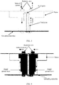
FIG. 2 is a schematic structural diagram of a radiating element in a multi-band antenna system in an existing mechanism; -
FIG. 3 is another schematic structural diagram of a radiating element in a multi-band antenna system in an existing mechanism; -
FIG. 4 is another schematic structural diagram of a radiating element in a multi-band antenna system in an existing mechanism; -
FIG. 5 is a schematic structural diagram of a multi-band antenna system according to an embodiment of the present invention; -
FIG. 6a is a schematic structural diagram of a first radiating element according to an embodiment of the present invention; -
FIG. 6b is another schematic structural diagram of a first radiating element according to an embodiment of the present invention; -
FIG. 6c is another schematic structural diagram of a first radiating element according to an embodiment of the present invention; -
FIG. 6d is another schematic structural diagram of a first radiating element according to an embodiment of the present invention; -
FIG. 6e is another schematic structural diagram of a first radiating element according to an embodiment of the present invention; -
FIG. 6f is another schematic structural diagram of a first radiating element according to an embodiment of the present invention; -
FIG. 7a is another schematic structural diagram of a first radiating element according to an embodiment of the present invention; -
FIG. 7b is another schematic structural diagram of a first radiating element according to an embodiment of the present invention; -
FIG. 7c is another schematic structural diagram of a first radiating element according to an embodiment of the present invention; -
FIG. 8 is another schematic structural diagram of a first radiating element according to an embodiment of the present invention; -
FIG. 9 is a schematic flowchart of a method for controlling inter-band interference in a multi-band antenna system according to an embodiment of the present invention; and -
FIG. 10 is a schematic diagram of a radiation gain curve according to an embodiment of the present invention. - In the specification, claims, and accompanying drawings of this application, the terms "first", "second", and so on are intended to distinguish between similar objects but do not necessarily indicate a specific order or sequence. It should be understood that data used in such a way is interchangeable in a proper circumstance, so that the embodiments described herein can be implemented in an order other than the order illustrated or described herein. In addition, the terms "include", "have", and any variant thereof are intended to cover non-exclusive inclusion. For example, a process, a method, a system, a product, or a device that includes a series of steps or modules is not necessarily limited to the steps or modules that are expressly listed, but may include another step or module not expressly listed or inherent to the process, the method, the product, or the device. The module division in this application is merely logical division, and there may be other division during implementation in actual application. For example, a plurality of modules may be combined or integrated into another system, or some features may be ignored or not performed. In addition, the displayed or discussed mutual couplings or direct couplings or communication connections may be implemented through some interfaces. Indirect couplings or communication connections between the modules may be implemented in an electronic or another form, and this is not limited in this application. In addition, modules or sub-modules described as separate components may be or may not be physically separated, or may be or may not be physical modules, or may not be distributed into a plurality of circuit modules. Objectives of the solutions of this application may be achieved by selecting some or all of the modules based on an actual requirement.
- This application provides a multi-band antenna system and a method for controlling inter-band interference in the multi-band antenna system, applicable to the field of antenna technologies. Detailed descriptions are provided below. The multi-band antenna system in this application includes a radiation arm, a balun, and a reflection apparatus. The balun refers to a balanced to unbalanced transformer, and the balun has functions of matching an unbalanced coaxial cable with a balanced dipole antenna, suppressing a common mode current, eliminating common-mode interference, and transforming impedance.
FIG. 3 is a schematic structural diagram of one side of a common balun, andFIG. 4 is a schematic structural diagram of another side of the common balun. A balun includes a feed plate, a microstrip, and a grounding structure. InFIG. 3 , a signal on a right side of the feed plate flows in a direction indicated by dashed line arrows (flowing upward), and a signal on a left side of the feed plate flows in a direction indicated by solid line arrows (flowing downward). The feed plate is separated, by using a medium, from a signal ground layer corresponding to the feed plate, and therefore currents on two signal ground layers are in an inverted phase. When the currents are in the inverted phase, radiation is offset. - However, because the radiation arm and the signal ground layers are electrically conductive and a current is continuous, signals on two radiation arms are in a same phase, and when the signals on the two radiation arms are in the same phase, radiation is enhanced. It can be learned that due to the feed plate structure in the balun, when a high-band radiating element is operating, if a nearby low-band radiating element is also operating, a radiation arm of the high-band radiating element obtains, through sensing, a corresponding low frequency signal. The low frequency signal may be transmitted from one radiation arm of the high-band radiating element to another radiation arm of the high-band radiating element by using a feed plate of the high-band radiating element, and may not directly flow into a grounding apparatus. In this way, an induced current in a same frequency band as the low frequency signal is formed between high-band radiation arms. This induced current generates differential mode radiation, and the differential mode radiation generated by the induced current is superposed on low-band radiation, used as a source, of the low-band radiating element. Consequently, normal operating of the low-band radiating element is interfered, and an antenna pattern may be distorted. It can be learned that the low frequency signal sensed by the high-band radiating element may be transmitted from one radiation arm to another radiation arm by using the feed plate of the high-band radiating element, to form the differential mode radiation, and the antenna pattern of the low-band radiating element is distorted.
- To resolve the foregoing technical problem, this application mainly provides the following technical solutions:
- A short-circuit stub may be introduced into a feed structure of the high-band radiating element, to divert a sensed differential mode signal to the grounding apparatus. Alternatively, a plated through hole is introduced into the feed structure of the high-band radiating element, to directly connect to a transport layer of a feed signal and the signal ground layer, so that the differential mode signal flows from a feed point to the microstrip, and finally flows from the microstrip to the grounding apparatus. In both of the two manners, differential mode radiation cannot be excited between the radiation arms of the high-band radiating element. Consequently, intensity of parasitic resonance generated in a low-band radiating element that has a relatively low operating frequency band decreases, and finally an antenna array of the low-band radiating element can operate normally.
- Referring to
FIG. 5 , the following uses an example to describe a structure of a multi-band antenna system provided in this application. The multi-band antenna system may include at least one first radiating element and at least one second radiating element. An operating frequency band of the first radiating element is higher than an operating frequency band of the second radiating element. The first radiating element and the second radiating element have different frequencies. When the first radiating element is operating, and nearby second radiation is also operating, this high-band element receives a signal of the second radiating element in two manners: a differential mode and a common mode. The following uses an example in which the first radiating element senses a differential mode signal of the second radiating element and suppresses flowing of the sensed differential mode signal into radiation arms of the first radiating element. - Each first radiating element includes a grounding structure, a balun, and at least two radiation arms. One end of the balun is electrically connected to the at least two radiation arms. The balun includes at least one conductive structure.
- The balun is configured to: after obtaining a differential mode signal, input the differential mode signal to the grounding structure by using the at least one conductive structure. The differential mode signal is a signal obtained by the balun by sensing a signal from the second radiating element in a differential mode manner.
- Optionally, the operating frequency band used by the first radiating element and that used by the second radiating element in this application may be in a frequency multiplication relationship, and a multiple of the operating frequency bands is not limited in this application.
- Compared with the prior art, in the solution provided in this application, because the at least one conductive structure is disposed in the balun in the first radiating element, after obtaining the differential mode signal, the balun can input the differential mode signal to the grounding structure by using the at least one conductive structure. In this way, the differential mode signal does not flow into the radiation arm of the first radiating element. Correspondingly, the differential mode signal does not generate differential mode radiation between radiation arms of the first radiating element, so that inter-band interference can be reduced, and differential mode resonance intensity of the second radiating element within the operating frequency band of the second radiating element decreases. Therefore, it can be ensured that the first radiating element operates normally, and the second radiating element also operates normally. For a high-band radiating element, after obtaining a low frequency signal of a low-band radiating element, because the high-band radiating element uses the balun structure shown in
FIG. 5 of this application, in other words, the high-band radiating element can block backflow of the low frequency signal between the radiation arms, the high-band radiating element finally eliminates the differential mode radiation caused by the low frequency signal. In this way, an antenna pattern of the low-band radiating element is not interfered, and a radiation gain of the low-band radiating element is further increased. - In this application, the balun further includes a transport layer of a feed signal, a signal ground layer, and a microstrip. Both the transport layer of the feed signal and the signal ground layer are electrically connected to the grounding structure. The transport layer of the feed signal is electrically connected to the signal ground layer, and the microstrip is electrically connected to the grounding structure. The following two manners are mainly used to suppress differential mode resonance.
- A. Introduce the short-circuit stub to the transport layer of the feed signal, and use the short-circuit stub and the microstrip as the conductive structure. When the conductive structure includes the short-circuit stub and the microstrip, the transport layer of the feed signal is used to: after obtaining the differential mode signal from the second radiating element, input the differential mode signal to the microstrip by using at least one short-circuit stub.
- The microstrip is configured to input, to the grounding structure, the differential mode signal input from the transport layer of the feed signal.
- In this application, the transport layer of the feed signal includes an impedance conversion section and a coupling section. The impedance conversion section includes a transmission section and a feed section. In this application, a total quantity of deployed short-circuit stubs and a quantity of short-circuit stubs respectively deployed on the transmission section, the feed section, or the coupling section is not limited. The following describes deployment of a short-circuit stub.
- When the at least one short-circuit stub is electrically connected to the transmission section, the differential mode signal flows from the transmission section and the feed section into the microstrip.
FIG. 6a is a schematic structural diagram when the short-circuit stub is disposed on the transmission section. - When the at least one short-circuit stub is electrically connected to the feed section, the differential mode signal flows from the feed section into the microstrip.
FIG. 6b is a schematic structural diagram when the short-circuit stub is disposed on the feed section. - When the at least one short-circuit stub is electrically connected to the coupling section, the differential mode signal flows from the coupling section and the feed section into the microstrip.
FIG. 6c is a schematic structural diagram when the short-circuit stub is disposed on the coupling section. - For example, the short-circuit stub is separately disposed on the transmission section and the coupling section (as shown in
FIG. 6d ), or the short-circuit stub is separately disposed on the feed section and the coupling section (as shown inFIG. 6e ), or the short-circuit stub is separately disposed on the transmission section, the feed section, and the coupling section (as shown inFIG. 6f ). - In this circuit structure in (4), a signal trend of the differential mode signal may include at least one of the following three types:
- The differential mode signal flows from the transmission section and the feed section into the microstrip.
- Alternatively, the differential mode signal flows from the coupling section and the feed section into the microstrip.
- Alternatively, the differential mode signal flows from the feed section into the microstrip.
- B. Introduce the short-circuit stub to the transport layer of the feed signal, and use the short-circuit stub as the conductive structure.
- One end of the short-circuit stub is electrically connected to the transport layer of the feed signal, and the other end of the short-circuit stub is electrically connected to the grounding structure.
- The transport layer of the feed signal is used to: after obtaining the differential mode signal, divert the differential mode signal from the transport layer of the feed signal to the grounding structure by using the at least one short-circuit stub, so that the differential mode signal cannot generate an induced current between the radiation arms of the first radiating element. In this way, differential mode resonance is not generated for the second radiating element, and a radiation gain of the second radiating element can be further increased without a need to greatly modify an original balun structure and to reduce an entire integration level of the balun.
- Likewise, in an embodiment in which the short-circuit stub is used as the conductive structure, and the differential mode signal is diverted to the grounding structure by using the short-circuit stub, the short-circuit stub may also be separately disposed on at least one of the transmission section, the feed section, or the coupling section. For a specific schematic structural diagram, refer to structural diagrams shown in
FIG. 7a, FIG. 7b , andFIG. 7c . InFIG. 7a , the short-circuit stub is disposed on the transmission section of the transport layer of the feed signal. InFIG. 7b , the short-circuit stub is disposed on the feed section of the transport layer of the feed signal. InFIG. 7c , the short-circuit stub is disposed on the coupling section of the transport layer of the feed signal. - Optionally, in some embodiments of the invention, an antenna element on the first radiating element is a half-wave dipole, to weaken impact on the differential mode resonance for the second radiating element, and ensure radiation efficiency of the first radiating element. Further, a length of the radiation arm of the first radiating element, a height of the balun of the first radiating element, or a length of the short-circuit stub may be set.
- For example, the height of the balun may be set to Y, where Y = L/4. The height of the balun is set to L/4 because a current on the radiation arm is parallel to a reflection apparatus. Due to the reflection apparatus, an equivalent mirror current having a mirror symmetry along the reflection apparatus in an opposite direction is generated. When the radiation arm is L/4 away from the reflection apparatus, the current on the radiation arm and the image current in a same phase may be superposed at a far field, thereby improving antenna performance.
- Alternatively, the length of the radiation arm is set to L/4, so that a total length of the two radiation arms is L/2, and maximum radiation efficiency can be finally implemented.
- For example, the length of the short-circuit stub may alternatively be set to X, where X = n x (L/4), L is a wavelength corresponding to a center frequency of the operating frequency band of the first radiating element, and n is a positive integer less than or equal to 4. For example, when n = 1, the length of the short-circuit stub is L/4, and the L/4 short-circuit stub considers impedance conversion of the transport layer of the feed signal. After L/4 conversion of the short-circuit stub on the entire transport layer of the feed signal, when a differential mode signal whose operating frequency is higher than that of a first high radiating element is obtained through sensing, a node impedance characteristic of the entire transport layer of the feed signal is an open circuit. Therefore, for a high frequency signal, the short-circuit stub of this length is equivalent to a short-circuit stub whose resistance is in a high resistance status, and is equivalent to an open circuit line. Therefore, a high-frequency differential mode signal cannot flow into the transport layer of the feed signal, but can only flow back between radiation arms at a top of the balun.
- However, for a low frequency signal, the short-circuit stub is not an L/4 open circuit line. Therefore, when a low-frequency differential mode signal flows into the first radiating element, a resistance of an entire short-circuit stub decreases. Therefore, the low-frequency differential mode signal may flow to the grounding structure along the microstrip, instead of flowing into the radiation arm of the first radiating element, to further eliminate differential mode resonance.
- Specifically, the plated through hole is introduced to the transport layer of the feed signal, and the plated through hole and the microstrip are used as the conductive structure. The plated through hole may be disposed at a stub of the feed section.
FIG. 8 is a schematic structural diagram when the plated through hole is disposed at the transport layer of the feed signal. - Correspondingly, the transport layer of the feed signal may be used to: after obtaining the differential mode signal, input the differential mode signal to the microstrip by using the plated through hole.
- The microstrip is configured to input, to the grounding structure, the differential mode signal input from the transport layer of the feed signal. The differential mode signal flows from the transmission section and the feed section into the microstrip.
- Specifically, when the plated through hole is disposed at the stub of the feed section, as shown in
FIG. 8 , on a left side ofFIG. 8 , the transport layer of the feed signal is directly electrically connected to the signal ground layer by using the plated through hole, and current flowing directions of the transport layer of the feed signal and the signal ground layer are consistent. On a right side ofFIG. 8 , the transport layer of the feed signal is connected, through coupling, to the signal ground layer by using a medium. It can be learned that currents at the transport layer of the feed signal and the signal ground layer are in a reverse phase. Solid line arrows on the right side ofFIG. 8 indicate a current direction of the transport layer of the feed signal on a right side of the radiation arm, and dashed line arrows on the right side ofFIG. 8 indicate a current direction of the signal ground layer on the right side of the radiation arm. In this case, for the high frequency signal, from the plated through hole used as a short circuit point, an impedance is infinite. However, for a low frequency signal obtained through sensing, because the plated through hole is disposed, a transmission path of the low-frequency induced current generated on the high-band radiating element is changed. Therefore, when obtaining, through sensing the low frequency signal, the high-band radiating element does not generate differential mode resonance that affects the low frequency signal. - It can be learned that in any one of circuit structures shown in
FIG. 5 to FIG. 8 , after the first radiating element obtains, through sensing, the differential mode signal of the second radiating element, differential mode resonance formed due to the differential mode signal on the first radiating element can be destroyed. For the second radiating element, radiation that is generated when the second radiating element is operating receives significantly less radiation interference from the first radiating element, and even does not receive radiation interference from the first radiating element. In addition, a radiation gain of the second radiating element does not deteriorate due to differential mode resonance. In comparison with an existing mechanism, the radiation gain of the second radiating element can be significantly increased. For a specific schematic diagram of radiation gain comparison, refer to the curve diagram shown inFIG. 10 . A dashed line inFIG. 10 is a radiation gain curve of the second radiating element when the balun structure in this application is not used. A solid line inFIG. 10 is a radiation gain curve of the second radiating element when the balun structure in this application is used. It may be learned fromFIG. 10 that the radiation gain of the second radiating element is significantly increased. - The foregoing uses an example to describe the multi-band antenna system, and the following uses an example to describe a method for controlling inter-band interference in the multi-band antenna system in this application. As shown in
FIG. 9 , in this embodiment of the present invention, the multi-band antenna system includes at least one first radiating element and at least one second radiating element, and an operating frequency band of the first radiating element is higher than an operating frequency band of the second radiating element. - Each first radiating element includes a grounding structure, a balun, and at least two radiation arms. One end of the balun is electrically connected to the at least two radiation arms. The balun includes at least one conductive structure. For a schematic structural diagram of the multi-band antenna system, refer to any one of structures shown in
FIG. 1, FIG. 2 , andFIG. 5 toFIG. 8 . - After the second radiating element sends a signal, if the first radiating element obtains, through sensing, the signal in a differential mode manner and obtains a differential mode signal, the first radiating element inputs the differential mode signal to the balun. After obtaining the differential mode signal, the balun transfers the differential mode signal to the grounding structure by using the at least one conductive structure. The differential mode signal is a signal obtained by the balun by sensing a signal from the second radiating element in a differential mode manner.
- In the solution provided in this application, because the at least one conductive structure is disposed in the balun in the first radiating element, after obtaining the differential mode signal, the balun can input the differential mode signal to the grounding structure by using the at least one conductive structure. In this way, the differential mode signal does not flow into the radiation arm of the first radiating element. Correspondingly, the differential mode signal does not generate differential mode radiation between radiation arms of the first radiating element, so that inter-band interference can be reduced, and differential mode resonance intensity of the second radiating element within the operating frequency band of the second radiating element decreases. Therefore, it can be ensured that the first radiating element operates normally, and the second radiating element also operates normally. For a high-band radiating element, after obtaining a low frequency signal of a low-band radiating element, because the high-band radiating element uses the balun structure shown in
FIG. 5 of this application, in other words, the high-band radiating element can block backflow of the low frequency signal between the radiation arms, the high-band radiating element finally eliminates the differential mode radiation caused by the low frequency signal. In this way, an antenna pattern of the low-band radiating element is not interfered, and a radiation gain of the low-band radiating element is further increased. - In this application, the balun further includes a transport layer of a feed signal, a signal ground layer, and a microstrip. Both the transport layer of the feed signal and the signal ground layer are electrically connected to the grounding structure. The transport layer of the feed signal is electrically connected to the signal ground layer, and the microstrip is electrically connected to the grounding structure. The following two manners are mainly used to suppress differential mode resonance.
- When the conductive structure includes the short-circuit stub and the microstrip, the transport layer of the feed signal inputs the differential mode signal to the microstrip by using at least one short-circuit stub.
- Then, the microstrip inputs, to the grounding structure, the differential mode signal input from the transport layer of the feed signal.
- In this application, the transport layer of the feed signal includes an impedance conversion section and a coupling section. The impedance conversion section includes a transmission section and a feed section. In this application, a total quantity of deployed short-circuit stubs and a quantity of short-circuit stubs respectively deployed on the transmission section, the feed section, or the coupling section is not limited. The following describes deployment of a short-circuit stub.
- When the at least one short-circuit stub is electrically connected to the transmission section, the differential mode signal flows from the transmission section and the feed section into the microstrip.
FIG. 6a is a schematic structural diagram when the short-circuit stub is disposed on the transmission section. Dashed line arrows on a left side of the balun shown inFIG. 6a refer to a direction of the differential mode signal in the microstrip, and dashed line arrows on a right side of the balun shown inFIG. 6a refer to a direction of the differential mode signal in the impedance conversion section. Because the differential mode signal cannot generate a flowing-back induced current between radiation arms, for the radiation arm of the first radiating element, currents of two radiation arms are in a same direction. In addition, there is no induced current generated by a differential mode signal of another radiating element whose operating frequency band is higher than that of the first radiating element. Finally, the first radiating element does not cause differential mode resonance interference to a second radiating element whose operating frequency band is lower than that of the first radiating element, or receive differential mode resonance interference from a nearby radiating element whose operating frequency band is higher than that of the first radiating element. - When the at least one short-circuit stub is electrically connected to the feed section, the differential mode signal flows from the feed section into the microstrip.
FIG. 6b is a schematic structural diagram when the short-circuit stub is disposed on the feed section. Dashed line arrows on a left side of the balun shown inFIG. 6b refer to a direction of the differential mode signal in the microstrip, and dashed line arrows on a right side of the balun shown inFIG. 6b refer to a direction of the differential mode signal in the impedance conversion section. - When the at least one short-circuit stub is electrically connected to the coupling section, the differential mode signal flows from the coupling section and the feed section into the microstrip.
FIG. 6c is a schematic structural diagram when the short-circuit stub is disposed on the coupling section. Dashed line arrows on a left side of the balun shown inFIG. 6c refer to a direction of the differential mode signal in the microstrip, and dashed line arrows on a right side of the balun shown inFIG. 6c refer to a direction of the differential mode signal in the impedance conversion section. - For example, the short-circuit stub is separately disposed on the transmission section and the coupling section (as shown in
FIG. 6d ), or the short-circuit stub is separately disposed on the feed section and the coupling section (as shown inFIG. 6e ), or the short-circuit stub is separately disposed on the transmission section, the feed section, and the coupling section (as shown inFIG. 6f ). For a specific trend of the differential mode signal, refer to the analysis process of the trend of the differential mode signal in the structures in (1) to (3). Specifically, in this circuit structure in (4), a signal trend of the differential mode signal may include at least one of the following three types: - The differential mode signal flows from the transmission section and the feed section into the microstrip.
- Alternatively, the differential mode signal flows from the coupling section and the feed section into the microstrip.
- Alternatively, the differential mode signal flows from the feed section into the microstrip.
- B. Introduce the short-circuit stub to the transport layer of the feed signal, and use the short-circuit stub as the foregoing conductive structure.
- One end of the short-circuit stub is electrically connected to the transport layer of the feed signal, and the other end of the short-circuit stub is electrically connected to the grounding structure.
- The transport layer of the feed signal is used to: after obtaining the differential mode signal, divert the differential mode signal from the transport layer of the feed signal to the grounding structure by using at least one short-circuit stub, so that the differential mode signal cannot generate an induced current between the radiation arms of the first radiating element. In this way, differential mode resonance is not generated for the second radiating element, and a radiation gain of the second radiating element can be increased without a need to greatly modify an original balun structure and to reduce an entire integration level of the balun.
- Likewise, in an embodiment in which the short-circuit stub is used as the conductive structure, and the differential mode signal is diverted to the grounding structure by using the short-circuit stub, the short-circuit stub may also be separately disposed on at least one of the transmission section, the feed section, or the coupling section. For a specific schematic structural diagram, refer to the structural diagrams shown in
FIG. 7a, FIG. 7b , andFIG. 7c . InFIG. 7a , the short-circuit stub is disposed on the transmission section of the transport layer of the feed signal. InFIG. 7b , the short-circuit stub is disposed on the feed section of the transport layer of the feed signal. InFIG. 7c , the short-circuit stub is disposed on the coupling section of the transport layer of the feed signal. - Optionally, in some embodiments of the invention, an antenna element on the first radiating element is a half-wave dipole, to weaken impact on the differential mode resonance for the second radiating element, and ensure radiation efficiency of the first radiating element. Further, a length of the radiation arm of the first radiating element, a height of the balun of the first radiating element, or a length of the short-circuit stub may be set.
- For example, the height of the balun may be Y, where Y = L/4, to enhance antenna performance of the first radiating element.
- Alternatively, the length of the radiation arm is set to L/4, so that a total length of the two radiation arms is L/2, and maximum radiation efficiency can be finally implemented.
- For example, the length of the short-circuit stub may alternatively be set to X, where X = n x (L/4), L is a wavelength corresponding to a center frequency of the operating frequency band of the first radiating element, and n is a positive integer less than or equal to 4. For example, when n = 1, the length of the short-circuit stub is L/4, and the L/4 short-circuit stub considers impedance conversion of the transport layer of the feed signal. After L/4 conversion of the short-circuit stub on the entire transport layer of the feed signal, for a high frequency signal, the short-circuit stub of this length is equivalent to a short-circuit stub whose resistance is in a high resistance status, and is equivalent to an open circuit line. Therefore, a high-frequency differential mode signal cannot flow into the transport layer of the feed signal, but can only flow back between radiation arms at a top of the balun.
- However, for a low frequency signal, the short-circuit stub is not an L/4 short circuit line. Therefore, when a low-frequency differential mode signal flows into the first radiating element, a resistance of an entire short-circuit stub decreases. Therefore, the low-frequency differential mode signal may flow to the grounding structure along the microstrip, instead of flowing into the radiation arm of the first radiating element, to further eliminate differential mode resonance.
- Specifically, the plated through hole is introduced to the transport layer of the feed signal, and the plated through hole and the microstrip are used as the conductive structure. The plated through hole may be disposed at a stub of the feed section.
FIG. 8 is a schematic structural diagram when the plated through hole is disposed at the transport layer of the feed signal. - Correspondingly, after obtaining the differential mode signal, the transport layer of the feed signal inputs the differential mode signal to the microstrip by using the plated through hole.
- Then, the microstrip inputs, to the grounding structure, the differential mode signal input from the transport layer of the feed signal. In the circuit structure shown in
FIG. 8 , the differential mode signal flows from the transmission section and the feed section into the microstrip. - Optionally, when the plated through hole is disposed at the stub of the feed section, as shown in
FIG. 8 , on a left side ofFIG. 8 , the transport layer of the feed signal is directly electrically connected to the signal ground layer by using the plated through hole, and current flowing directions of the transport layer of the feed signal and the signal ground layer are consistent. On a right side ofFIG. 8 , the transport layer of the feed signal is connected, through coupling, to the signal ground layer by using a medium. It can be learned that currents in the transport layer of the feed signal and the signal ground layer are in a reverse phase. Solid line arrows on the right side ofFIG. 8 indicate a current direction of the transport layer of the feed signal on a right side of the radiation arm, and dashed line arrows on the right side ofFIG. 8 indicate a current direction of the signal ground layer on the right side of the radiation arm. In this case, for the high frequency signal, from the plated through hole used as a short circuit point, an impedance is infinite. However, for a low frequency signal obtained through sensing, because the plated through hole is disposed, a transmission path of the low-frequency induced current generated on the high-band radiating element is changed. Therefore, when obtaining, through sensing the low frequency signal, the high-band radiating element does not generate differential mode resonance that affects the low frequency signal. - It can be learned that in any one of circuit structures shown in
FIG. 5 to FIG. 8 , after the first radiating element obtains, through sensing, the differential mode signal of the second radiating element, differential mode resonance formed due to the differential mode signal on the first radiating element can be destroyed. For the second radiating element, radiation that is generated when the second radiating element is operating receives significantly less radiation interference from the first radiating element, and even does not receive radiation interference from the first radiating element. In addition, a radiation gain of the second radiating element does not deteriorate due to differential mode resonance. In comparison with an existing mechanism, the radiation gain of the second radiating element can be significantly increased. For a specific schematic diagram of radiation gain comparison, refer to the curve diagram shown inFIG. 10 . A dashed line inFIG. 10 is a radiation gain curve of the second radiating element when the balun structure in this application is not used. A solid line inFIG. 10 is a radiation gain curve of the second radiating element when the balun structure in this application is used. It may be learned fromFIG. 10 that the radiation gain of the second radiating element is significantly increased. - Optionally, in some embodiments of the invention, if a signal sent on at least one low frequency band is received on a plurality of high frequency bands at a same time, in other words, a plurality of first radiating elements receive, at a same time, a signal sent by at least one second radiating element, for a process of processing the signal on each high-band radiating element, refer to description of the first radiating element in the foregoing embodiment. Details are not described herein. For an entire multi-band antenna system, a total effect generated is a sum of superposed vectors. To be specific, a low-band element is first placed, and a differential mode resonance suppression procedure (a differential mode resonance suppression procedure of the first radiating element) is performed on each high-band element in the multi-band antenna system. However, induced current intensity of each high-band radiating element may be different (induced current intensity is inversely proportional to a square of a distance, for example, a longer distance indicates weaker induced current intensity). If low-band radiating elements are deployed in different places, induced current intensity on a high-band radiating element near the low-band radiating element also changes, and a change principle is consistent. Finally, for a specific high-band radiating element, when a plurality of low-band radiating elements are deployed around the high-band radiating element, induced current generated on the high-band radiating element is equal to a vector sum of induced currents generated when each low frequency band exists individually. In the foregoing embodiments, the description of all embodiments has respective focuses. For a part that is not described in detail in an embodiment, refer to related description in another embodiment.
- It may be clearly understood by a person skilled in the art that, for convenient and brief description, for a specific working process of the foregoing system, apparatus, and module, refer to a corresponding process in the foregoing method embodiments. Details are not described herein again.
- In the several embodiments provided in this application, it should be understood that the disclosed system, apparatus, and method may be implemented in other manners. For example, the described apparatus embodiment is merely an example. For example, the module division is merely logical function division and may be other division during actual implementation. For example, a plurality of modules or components may be combined or integrated into another system, or some features may be ignored or not performed. In addition, the displayed or discussed mutual couplings or direct couplings or communication connections may be implemented through some interfaces. The indirect couplings or communication connections between the apparatuses or modules may be implemented in electronic, mechanical, or other forms.
- The modules described as separate parts may or may not be physically separate, and parts displayed as modules may or may not be physical modules, may be located in one position, or may be distributed on a plurality of network modules. Some or all the modules may be selected based on an actual requirement to achieve the objectives of the solutions of the embodiments.
- In addition, functional modules in the embodiments of this application may be integrated into one processing module, or each of the modules may exist alone physically, or two or more modules are integrated into one module. The integrated module may be implemented in a form of hardware, or may be implemented in a form of a software functional module. When the integrated module is implemented in the form of the software functional module and sold or used as an independent product, the integrated module may be stored in a computer-readable storage medium.
- All or some of the foregoing embodiments may be implemented by using software, hardware, firmware, or any combination thereof. When the embodiments are implemented by using software, all or some of the embodiments may be implemented in a form of a computer program product.
- The computer program product includes one or more computer instructions. When the computer program instruction is loaded and executed on a computer, the procedure or function according to the embodiments of the present invention are all or partially generated. The computer may be a general-purpose computer, a dedicated computer, a computer network, or another programmable apparatus. The computer instructions may be stored in a computer-readable storage medium or may be transmitted from one computer-readable storage medium to another computer-readable storage medium. For example, the computer instruction may be transmitted from one website, computer, server, or data center to another website, computer, server, or data center in a wired (for example, a coaxial cable, an optical fiber, or a digital subscriber line (DSL)) or wireless (for example, infrared, radio, or microwave) manner. The computer-readable storage medium may be any usable medium accessible by a computer, or a data storage device, such as a server or a data center, integrating one or more usable media. The usable medium may be a magnetic medium (for example, a floppy disk, a hard disk, or a magnetic tape), an optical medium (for example, a DVD), a semiconductor medium (for example, a solid-state drive Solid State Disk (SSD)), or the like.
- The technical solutions provided in this application are described in detail above. The principle and implementation of this application are described herein by using specific examples. The description about the embodiments is merely provided to help understand the method and core ideas of this application. In addition, a person of ordinary skill in the art can make variations and modifications to this application in terms of the specific implementations and application scopes based on the ideas of this application. Therefore, the content of specification shall not be construed as a limit to this application.
Claims (19)
- A multi-band antenna system, comprising at least one first radiating element and at least one second radiating element, wherein an operating frequency band of the first radiating element is higher than an operating frequency band of the second radiating element;each first radiating element comprises a grounding structure, a balun, and at least two radiation arms, one end of the balun is electrically connected to the at least two radiation arms, the balun comprises at least one conductive structure, and the conductive structure is electrically connected to the grounding structure; andthe balun is configured to: after obtaining a differential mode signal, input the differential mode signal to the grounding structure by using the at least one conductive structure, wherein the differential mode signal is a signal obtained by the balun by sensing a signal from the second radiating element in a differential mode manner.
- The antenna system according to claim 1, wherein the balun further comprises a transport layer of a feed signal, the transport layer of the feed signal is electrically connected to the conductive structure, the conductive structure comprises a short-circuit stub and a microstrip, and the microstrip is electrically connected to the grounding structure;the transport layer of the feed signal is configured to: after obtaining the differential mode signal, input the differential mode signal to the microstrip by using at least one short-circuit stub; andthe microstrip is configured to input, to the grounding structure, the differential mode signal input from the transport layer of the feed signal.
- The antenna system according to claim 2, wherein the transport layer of the feed signal comprises an impedance conversion section, and the impedance conversion section comprises a transmission section and a feed section, such thatwhen the at least one short-circuit stub is electrically connected to the transmission section, the differential mode signal flows from the transmission section and the feed section into the microstrip; orwhen the at least one short-circuit stub is electrically connected to the feed section, the differential mode signal flows from the feed section into the microstrip.
- The antenna system according to claim 2, wherein the transport layer of the feed signal comprises an impedance conversion section and a coupling section, the impedance conversion section comprises a feed section, and the at least one short-circuit stub is electrically connected to the coupling section, such that the differential mode signal flows from the coupling section and the feed section into the
- The antenna system according to claim 2, wherein the transport layer of the feed signal comprises an impedance conversion section and a coupling section, the coupling section and the impedance conversion section each are electrically connected to the at least one short-circuit stub, and the impedance conversion section comprises a transmission section and a feed section, such thatthe differential mode signal flows from the transmission section and the feed section into the microstrip; orthe differential mode signal flows from the coupling section and the feed section into the microstrip; orthe differential mode signal flows from the feed section into the microstrip.
- The antenna system according to claim 1, wherein the balun further comprises a transport layer of a feed signal, the transport layer of the feed signal is electrically connected to the conductive structure, the conductive structure comprises a short-circuit stub, one end of the short-circuit stub is electrically connected to the transport layer of the feed signal, and the other end of the short-circuit stub is electrically connected to the grounding structure; and
the transport layer of the feed signal is configured to: after obtaining the differential mode signal, divert the differential mode signal from the transport layer of the feed signal to the grounding structure by using the at least one short-circuit stub. - The antenna system according to claim 1, wherein the balun further comprises a transport layer of a feed signal, the transport layer of the feed signal is electrically connected to the conductive structure, the conductive structure comprises a microstrip and a plated through hole, the plated through hole is disposed at a stub of a feed section, and the microstrip is electrically connected to the grounding structure;the transport layer of the feed signal is configured to: after obtaining the differential mode signal from the second radiating element, input the differential mode signal to the microstrip by using the plated through hole; andthe microstrip is configured to input, to the grounding structure, the differential mode signal input from the transport layer of the feed signal.
- The antenna system according to claim 7, wherein the transport layer of the feed signal comprises an impedance conversion section, and the impedance conversion section comprises a transmission section and the feed section, such that the differential mode signal flows from the transmission section and the feed section into the microstrip.
- The antenna system according to any one of claims 2 to 6, wherein a length of the short-circuit stub is X, X = n x (L/4), L is a wavelength corresponding to a center frequency of the operating frequency band of the first radiating element, and n is a positive integer less than or equal to 4.
- The antenna system according to claim 8, wherein a height of the balun is Y, and Y = L/4.
- A method for controlling inter-band interference in a multi-band antenna system, wherein the multi-band antenna system comprises at least one first radiating element and at least one second radiating element, and an operating frequency band of the first radiating element is higher than an operating frequency band of the second radiating element; and
each first radiating element comprises a grounding structure, a balun, and at least two radiation arms, one end of the balun is electrically connected to the at least two radiation arms, the balun comprises at least one conductive structure, and the conductive structure is electrically connected to the grounding structure; and the method comprises:
after obtaining a differential mode signal, transferring, by the balun, the differential mode signal to the grounding structure by using the at least one conductive structure, wherein the differential mode signal is a signal obtained by the balun by sensing a signal from the second radiating element in a differential mode manner. - The method according to claim 11, wherein the balun further comprises a transport layer of a feed signal, the transport layer of the feed signal is electrically connected to the conductive structure, the conductive structure comprises a short-circuit stub and a microstrip, and the microstrip is electrically connected to the grounding structure; and
the transferring the differential mode signal to the grounding structure by using the at least one conductive structure comprises:inputting, by the transport layer of the feed signal, the differential mode signal to the microstrip by using the at least one short-circuit stub; andinputting, by the microstrip to the grounding structure, the differential mode signal input from the transport layer of the feed signal. - The method according to claim 12, wherein the transport layer of the feed signal comprises an impedance conversion section, and the impedance conversion section comprises a transmission section and a feed section; andwhen the at least one short-circuit stub is electrically connected to the transmission section, the differential mode signal flows from the transmission section and the feed section into the microstrip; orwhen the at least one short-circuit stub is electrically connected to the feed section, the differential mode signal flows from the feed section into the microstrip.
- The method according to claim 12, wherein the transport layer of the feed signal comprises an impedance conversion section and a coupling section, the impedance conversion section comprises a feed section, and the at least one short-circuit stub is electrically connected to the coupling section; and
the differential mode signal flows from the coupling section and the feed section into the microstrip. - The method according to claim 12, wherein the transport layer of the feed signal comprises an impedance conversion section and a coupling section, the coupling section and the impedance conversion section each are electrically connected to the at least one short-circuit stub, and the impedance conversion section comprises a transmission section and a feed section; andthe differential mode signal flows from the transmission section and the feed section into the microstrip; orthe differential mode signal flows from the coupling section and the feed section into the microstrip; orthe differential mode signal flows from the feed section into the microstrip.
- The method according to claim 11, wherein the balun further comprises a transport layer of a feed signal, the transport layer of the feed signal is electrically connected to the conductive structure, the conductive structure comprises a short-circuit stub, one end of the short-circuit stub is electrically connected to the transport layer of the feed signal, and the other end of the short-circuit stub is electrically connected to the grounding structure; and
the transferring the differential mode signal to the grounding structure by using the at least one conductive structure comprises:
after obtaining the differential mode signal, diverting, by the transport layer of the feed signal, the differential mode signal from the transport layer of the feed signal to the grounding structure by using the at least one short-circuit stub. - The method according to claim 11, wherein the balun further comprises a transport layer of a feed signal, the transport layer of the feed signal is electrically connected to the conductive structure, the conductive structure comprises a microstrip and a plated through hole, the plated through hole is disposed at a stub of a feed section, and the microstrip is electrically connected to the grounding structure; and
the transferring the differential mode signal to the grounding structure by using the at least one conductive structure comprises:after obtaining the differential mode signal, inputting, by the transport layer of the feed signal, the differential mode signal to the microstrip by using the plated through hole; andinputting, by the microstrip to the grounding structure, the differential mode signal input from the transport layer of the feed signal. - The method according to claim 17, wherein the transport layer of the feed signal comprises an impedance conversion section, the impedance conversion section comprises a transmission section and the feed section, and the plated through hole is disposed at the stub of the feed section; and
the differential mode signal flows from the transmission section and the feed section into the microstrip. - The method according to any one of claims 12 to 16, wherein a length of the short-circuit stub is X, X = n x (L/4), L is a wavelength corresponding to a center frequency of the operating frequency band of the first radiating element, and n is a positive integer less than or equal to 4.
Applications Claiming Priority (2)
| Application Number | Priority Date | Filing Date | Title |
|---|---|---|---|
| CN201710401145.6A CN107359418B (en) | 2017-05-31 | 2017-05-31 | A kind of method of alien frequencies interference in frequency antenna system and control frequency antenna system |
| PCT/CN2018/089239 WO2018219321A1 (en) | 2017-05-31 | 2018-05-31 | Multi-frequency antenna system, and method for controlling different frequency interference in multi-frequency antenna system |
Publications (3)
| Publication Number | Publication Date |
|---|---|
| EP3618186A1 EP3618186A1 (en) | 2020-03-04 |
| EP3618186A4 EP3618186A4 (en) | 2020-05-06 |
| EP3618186B1 true EP3618186B1 (en) | 2021-12-15 |
Family
ID=60271747
Family Applications (1)
| Application Number | Title | Priority Date | Filing Date |
|---|---|---|---|
| EP18809449.4A Active EP3618186B1 (en) | 2017-05-31 | 2018-05-31 | Multi-frequency antenna system, and method for controlling different frequency interference in a multi-frequency antenna system |
Country Status (5)
| Country | Link |
|---|---|
| US (1) | US11322834B2 (en) |
| EP (1) | EP3618186B1 (en) |
| CN (1) | CN107359418B (en) |
| BR (1) | BR112019025261A2 (en) |
| WO (1) | WO2018219321A1 (en) |
Families Citing this family (19)
| Publication number | Priority date | Publication date | Assignee | Title |
|---|---|---|---|---|
| CN107359418B (en) * | 2017-05-31 | 2019-11-29 | 上海华为技术有限公司 | A kind of method of alien frequencies interference in frequency antenna system and control frequency antenna system |
| CN109841963B (en) * | 2017-11-28 | 2021-06-15 | 华为技术有限公司 | A feeder system, antenna system and base station |
| CN110931952B (en) * | 2018-09-20 | 2021-12-24 | 上海华为技术有限公司 | Multi-frequency antenna and communication device |
| CN111313155B (en) * | 2018-12-11 | 2021-11-19 | 华为技术有限公司 | Antenna and communication apparatus |
| CN111384594B (en) * | 2018-12-29 | 2021-07-09 | 华为技术有限公司 | High-frequency radiators, multi-frequency array antennas and base stations |
| CN113782953B (en) | 2019-02-19 | 2025-09-12 | 华为技术有限公司 | Radiating device and multi-band array antenna |
| CN110098471B (en) * | 2019-03-14 | 2020-09-22 | 重庆大学 | A broadband dual-polarized base station antenna based on hybrid balun |
| CN112688052B (en) * | 2019-10-18 | 2022-04-26 | 华为技术有限公司 | Common-aperture antenna and communication equipment |
| CN111048898B (en) * | 2019-12-31 | 2022-12-27 | 京信通信技术(广州)有限公司 | Antenna and radiating element thereof |
| CN113937490B (en) * | 2020-07-13 | 2023-05-16 | 华为技术有限公司 | Antenna and wireless device |
| CN113948865A (en) | 2020-07-15 | 2022-01-18 | 华为技术有限公司 | Dual-frequency antenna and antenna array |
| GB2601810B (en) * | 2020-12-11 | 2023-07-05 | Alpha Wireless Ltd | High band antenna elements and a multi-band antenna |
| CN112768895B (en) * | 2020-12-29 | 2022-05-03 | 华南理工大学 | Antenna, low-frequency oscillator and radiating element |
| CN116014419B (en) * | 2021-10-22 | 2026-03-24 | 华为技术有限公司 | An antenna and a communication device |
| CN116111343A (en) * | 2021-11-11 | 2023-05-12 | 华为技术有限公司 | Feed network, antenna device and communication equipment |
| WO2024076946A1 (en) * | 2022-10-07 | 2024-04-11 | Commscope Technologies Llc | Cross-dipole radiating elements having feed stalks that exhibit improved cloaking performance and base station antennas including such radiating elements |
| CN118431735A (en) * | 2023-01-31 | 2024-08-02 | 华为技术有限公司 | Antennas and communication equipment |
| CN116073127B (en) * | 2023-04-07 | 2023-06-06 | 微网优联科技(成都)有限公司 | Super-surface loading base station antenna |
| CN119029538A (en) * | 2024-09-03 | 2024-11-26 | 佛山市迪安通讯设备有限公司 | A broadband single-polarized half-wave oscillator and communication equipment |
Family Cites Families (13)
| Publication number | Priority date | Publication date | Assignee | Title |
|---|---|---|---|---|
| CN1572045A (en) | 2001-08-31 | 2005-01-26 | 纽约市哥伦比亚大学托管会 | Systems and methods for providing optimized patch antenna excitation for mutually coupled patches |
| CN201174424Y (en) * | 2008-02-20 | 2008-12-31 | 广东通宇通讯设备有限公司 | Integrated designed multi-frequency radiation antenna |
| CN101944649A (en) * | 2010-08-09 | 2011-01-12 | 洪国智 | Antenna module |
| WO2013109173A1 (en) | 2012-01-17 | 2013-07-25 | Saab Ab | Combined antenna, antenna array and method for using the array antenna |
| CN102868017B (en) * | 2012-08-31 | 2015-05-13 | 广东通宇通讯股份有限公司 | Radiation device and array antenna based on same |
| US9329255B2 (en) * | 2013-06-24 | 2016-05-03 | Raytheon Company | Imaging antenna and related techniques |
| US9490542B1 (en) * | 2014-01-17 | 2016-11-08 | Stellenbosch University | Multi-mode composite antenna |
| CN104064867B (en) * | 2014-06-12 | 2016-10-05 | 京信通信技术(广州)有限公司 | Multiband radiating element and mobile communication antenna |
| EP3245691B1 (en) * | 2015-01-15 | 2020-09-16 | Commscope Technologies LLC | Low common mode resonance multiband radiating array |
| CN105960737B (en) * | 2015-12-03 | 2019-08-20 | 华为技术有限公司 | A kind of multi-band communication antenna and base station |
| CN105576378B (en) * | 2015-12-17 | 2018-11-13 | 京信通信系统(广州)有限公司 | A kind of dual-band antenna, dual polarization dual-band antenna and isolation element preparation method |
| CN106025555A (en) * | 2016-05-19 | 2016-10-12 | 西安电子科技大学 | Broadband dual polarization dipole antenna |
| CN107359418B (en) * | 2017-05-31 | 2019-11-29 | 上海华为技术有限公司 | A kind of method of alien frequencies interference in frequency antenna system and control frequency antenna system |
-
2017
- 2017-05-31 CN CN201710401145.6A patent/CN107359418B/en active Active
-
2018
- 2018-05-31 WO PCT/CN2018/089239 patent/WO2018219321A1/en not_active Ceased
- 2018-05-31 EP EP18809449.4A patent/EP3618186B1/en active Active
- 2018-05-31 BR BR112019025261-4A patent/BR112019025261A2/en unknown
-
2019
- 2019-11-26 US US16/696,744 patent/US11322834B2/en active Active
Also Published As
| Publication number | Publication date |
|---|---|
| US20200099130A1 (en) | 2020-03-26 |
| US11322834B2 (en) | 2022-05-03 |
| CN107359418B (en) | 2019-11-29 |
| BR112019025261A2 (en) | 2020-09-01 |
| WO2018219321A1 (en) | 2018-12-06 |
| CN107359418A (en) | 2017-11-17 |
| EP3618186A1 (en) | 2020-03-04 |
| EP3618186A4 (en) | 2020-05-06 |
Similar Documents
| Publication | Publication Date | Title |
|---|---|---|
| US11322834B2 (en) | Multi-band antenna system and method for controlling inter-band interference in multi-band antenna system | |
| CN113991287B (en) | Antenna assembly and mobile terminal | |
| US20200235459A1 (en) | Portable terminal with antenna device for display element or display assembly including flexible functional region | |
| EP3373390B1 (en) | Multi-frequency communication antenna and base station | |
| JP6562945B2 (en) | Apparatus, method and computing device having an isolator assembly | |
| WO2020259663A1 (en) | Foldable mobile terminal and antenna control method | |
| TWI466381B (en) | Mobile communication device and antenna thereof | |
| CN209860131U (en) | Electronic device | |
| US8525731B2 (en) | Small antenna using SRR structure in wireless communication system and method for manufacturing the same | |
| EP2851997A1 (en) | Printed circuit board antenna and printed circuit board | |
| CN109672019B (en) | Terminal MIMO antenna device and method for realizing antenna signal transmission | |
| JP5908486B2 (en) | MIMO antenna system | |
| WO2011102143A1 (en) | Antenna device and portable wireless terminal equipped with same | |
| TWI594504B (en) | Wireless communication device | |
| CN110199435A (en) | Mobile device with multiple antenna system | |
| JP2021507553A (en) | Antennas and terminals | |
| CN112768959A (en) | Antenna assembly and electronic equipment | |
| JP2013168756A (en) | Antenna device and radio communication device | |
| CN114696078B (en) | Antenna devices and electronic equipment | |
| CN110048230A (en) | Compact aerial and mobile terminal | |
| EP3065215A1 (en) | Multi-input multi-output (mimo) antenna | |
| JP2010103841A (en) | Antenna apparatus and wireless communication device | |
| WO2018157661A1 (en) | Antenna and terminal | |
| WO2024097557A1 (en) | Multiple pifa/ifa type antennas operating at the same frequency including short pins to minimize antenna separation | |
| JP3838971B2 (en) | Wireless device |
Legal Events
| Date | Code | Title | Description |
|---|---|---|---|
| STAA | Information on the status of an ep patent application or granted ep patent |
Free format text: STATUS: THE INTERNATIONAL PUBLICATION HAS BEEN MADE |
|
| PUAI | Public reference made under article 153(3) epc to a published international application that has entered the european phase |
Free format text: ORIGINAL CODE: 0009012 |
|
| STAA | Information on the status of an ep patent application or granted ep patent |
Free format text: STATUS: REQUEST FOR EXAMINATION WAS MADE |
|
| 17P | Request for examination filed |
Effective date: 20191126 |
|
| AK | Designated contracting states |
Kind code of ref document: A1 Designated state(s): AL AT BE BG CH CY CZ DE DK EE ES FI FR GB GR HR HU IE IS IT LI LT LU LV MC MK MT NL NO PL PT RO RS SE SI SK SM TR |
|
| AX | Request for extension of the european patent |
Extension state: BA ME |
|
| A4 | Supplementary search report drawn up and despatched |
Effective date: 20200407 |
|
| RIC1 | Information provided on ipc code assigned before grant |
Ipc: H01Q 5/50 20150101ALI20200401BHEP Ipc: H01Q 1/52 20060101AFI20200401BHEP Ipc: H01Q 5/307 20150101ALI20200401BHEP |
|
| DAV | Request for validation of the european patent (deleted) | ||
| DAX | Request for extension of the european patent (deleted) | ||
| REG | Reference to a national code |
Ref country code: DE Ref legal event code: R079 Ref document number: 602018028316 Country of ref document: DE Free format text: PREVIOUS MAIN CLASS: H01Q0005100000 Ipc: H01Q0001520000 |
|
| GRAP | Despatch of communication of intention to grant a patent |
Free format text: ORIGINAL CODE: EPIDOSNIGR1 |
|
| STAA | Information on the status of an ep patent application or granted ep patent |
Free format text: STATUS: GRANT OF PATENT IS INTENDED |
|
| RIC1 | Information provided on ipc code assigned before grant |
Ipc: H01Q 1/52 20060101AFI20210618BHEP Ipc: H01Q 5/307 20150101ALI20210618BHEP Ipc: H01Q 5/50 20150101ALI20210618BHEP Ipc: H01Q 21/26 20060101ALN20210618BHEP |
|
| INTG | Intention to grant announced |
Effective date: 20210714 |
|
| GRAS | Grant fee paid |
Free format text: ORIGINAL CODE: EPIDOSNIGR3 |
|
| GRAA | (expected) grant |
Free format text: ORIGINAL CODE: 0009210 |
|
| STAA | Information on the status of an ep patent application or granted ep patent |
Free format text: STATUS: THE PATENT HAS BEEN GRANTED |
|
| AK | Designated contracting states |
Kind code of ref document: B1 Designated state(s): AL AT BE BG CH CY CZ DE DK EE ES FI FR GB GR HR HU IE IS IT LI LT LU LV MC MK MT NL NO PL PT RO RS SE SI SK SM TR |
|
| REG | Reference to a national code |
Ref country code: GB Ref legal event code: FG4D Ref country code: CH Ref legal event code: EP |
|
| REG | Reference to a national code |
Ref country code: IE Ref legal event code: FG4D Ref country code: DE Ref legal event code: R096 Ref document number: 602018028316 Country of ref document: DE |
|
| REG | Reference to a national code |
Ref country code: AT Ref legal event code: REF Ref document number: 1456175 Country of ref document: AT Kind code of ref document: T Effective date: 20220115 |
|
| REG | Reference to a national code |
Ref country code: LT Ref legal event code: MG9D |
|
| REG | Reference to a national code |
Ref country code: NL Ref legal event code: MP Effective date: 20211215 |
|
| PG25 | Lapsed in a contracting state [announced via postgrant information from national office to epo] |
Ref country code: RS Free format text: LAPSE BECAUSE OF FAILURE TO SUBMIT A TRANSLATION OF THE DESCRIPTION OR TO PAY THE FEE WITHIN THE PRESCRIBED TIME-LIMIT Effective date: 20211215 Ref country code: LT Free format text: LAPSE BECAUSE OF FAILURE TO SUBMIT A TRANSLATION OF THE DESCRIPTION OR TO PAY THE FEE WITHIN THE PRESCRIBED TIME-LIMIT Effective date: 20211215 Ref country code: FI Free format text: LAPSE BECAUSE OF FAILURE TO SUBMIT A TRANSLATION OF THE DESCRIPTION OR TO PAY THE FEE WITHIN THE PRESCRIBED TIME-LIMIT Effective date: 20211215 Ref country code: BG Free format text: LAPSE BECAUSE OF FAILURE TO SUBMIT A TRANSLATION OF THE DESCRIPTION OR TO PAY THE FEE WITHIN THE PRESCRIBED TIME-LIMIT Effective date: 20220315 |
|
| REG | Reference to a national code |
Ref country code: AT Ref legal event code: MK05 Ref document number: 1456175 Country of ref document: AT Kind code of ref document: T Effective date: 20211215 |
|
| PG25 | Lapsed in a contracting state [announced via postgrant information from national office to epo] |
Ref country code: SE Free format text: LAPSE BECAUSE OF FAILURE TO SUBMIT A TRANSLATION OF THE DESCRIPTION OR TO PAY THE FEE WITHIN THE PRESCRIBED TIME-LIMIT Effective date: 20211215 Ref country code: NO Free format text: LAPSE BECAUSE OF FAILURE TO SUBMIT A TRANSLATION OF THE DESCRIPTION OR TO PAY THE FEE WITHIN THE PRESCRIBED TIME-LIMIT Effective date: 20220315 Ref country code: LV Free format text: LAPSE BECAUSE OF FAILURE TO SUBMIT A TRANSLATION OF THE DESCRIPTION OR TO PAY THE FEE WITHIN THE PRESCRIBED TIME-LIMIT Effective date: 20211215 Ref country code: HR Free format text: LAPSE BECAUSE OF FAILURE TO SUBMIT A TRANSLATION OF THE DESCRIPTION OR TO PAY THE FEE WITHIN THE PRESCRIBED TIME-LIMIT Effective date: 20211215 Ref country code: GR Free format text: LAPSE BECAUSE OF FAILURE TO SUBMIT A TRANSLATION OF THE DESCRIPTION OR TO PAY THE FEE WITHIN THE PRESCRIBED TIME-LIMIT Effective date: 20220316 |
|
| PG25 | Lapsed in a contracting state [announced via postgrant information from national office to epo] |
Ref country code: NL Free format text: LAPSE BECAUSE OF FAILURE TO SUBMIT A TRANSLATION OF THE DESCRIPTION OR TO PAY THE FEE WITHIN THE PRESCRIBED TIME-LIMIT Effective date: 20211215 |
|
| PG25 | Lapsed in a contracting state [announced via postgrant information from national office to epo] |
Ref country code: SM Free format text: LAPSE BECAUSE OF FAILURE TO SUBMIT A TRANSLATION OF THE DESCRIPTION OR TO PAY THE FEE WITHIN THE PRESCRIBED TIME-LIMIT Effective date: 20211215 Ref country code: SK Free format text: LAPSE BECAUSE OF FAILURE TO SUBMIT A TRANSLATION OF THE DESCRIPTION OR TO PAY THE FEE WITHIN THE PRESCRIBED TIME-LIMIT Effective date: 20211215 Ref country code: RO Free format text: LAPSE BECAUSE OF FAILURE TO SUBMIT A TRANSLATION OF THE DESCRIPTION OR TO PAY THE FEE WITHIN THE PRESCRIBED TIME-LIMIT Effective date: 20211215 Ref country code: PT Free format text: LAPSE BECAUSE OF FAILURE TO SUBMIT A TRANSLATION OF THE DESCRIPTION OR TO PAY THE FEE WITHIN THE PRESCRIBED TIME-LIMIT Effective date: 20220418 Ref country code: ES Free format text: LAPSE BECAUSE OF FAILURE TO SUBMIT A TRANSLATION OF THE DESCRIPTION OR TO PAY THE FEE WITHIN THE PRESCRIBED TIME-LIMIT Effective date: 20211215 Ref country code: EE Free format text: LAPSE BECAUSE OF FAILURE TO SUBMIT A TRANSLATION OF THE DESCRIPTION OR TO PAY THE FEE WITHIN THE PRESCRIBED TIME-LIMIT Effective date: 20211215 Ref country code: CZ Free format text: LAPSE BECAUSE OF FAILURE TO SUBMIT A TRANSLATION OF THE DESCRIPTION OR TO PAY THE FEE WITHIN THE PRESCRIBED TIME-LIMIT Effective date: 20211215 |
|
| PG25 | Lapsed in a contracting state [announced via postgrant information from national office to epo] |
Ref country code: PL Free format text: LAPSE BECAUSE OF FAILURE TO SUBMIT A TRANSLATION OF THE DESCRIPTION OR TO PAY THE FEE WITHIN THE PRESCRIBED TIME-LIMIT Effective date: 20211215 Ref country code: AT Free format text: LAPSE BECAUSE OF FAILURE TO SUBMIT A TRANSLATION OF THE DESCRIPTION OR TO PAY THE FEE WITHIN THE PRESCRIBED TIME-LIMIT Effective date: 20211215 |
|
| REG | Reference to a national code |
Ref country code: DE Ref legal event code: R097 Ref document number: 602018028316 Country of ref document: DE |
|
| PG25 | Lapsed in a contracting state [announced via postgrant information from national office to epo] |
Ref country code: IS Free format text: LAPSE BECAUSE OF FAILURE TO SUBMIT A TRANSLATION OF THE DESCRIPTION OR TO PAY THE FEE WITHIN THE PRESCRIBED TIME-LIMIT Effective date: 20220415 |
|
| PLBE | No opposition filed within time limit |
Free format text: ORIGINAL CODE: 0009261 |
|
| STAA | Information on the status of an ep patent application or granted ep patent |
Free format text: STATUS: NO OPPOSITION FILED WITHIN TIME LIMIT |
|
| PG25 | Lapsed in a contracting state [announced via postgrant information from national office to epo] |
Ref country code: DK Free format text: LAPSE BECAUSE OF FAILURE TO SUBMIT A TRANSLATION OF THE DESCRIPTION OR TO PAY THE FEE WITHIN THE PRESCRIBED TIME-LIMIT Effective date: 20211215 Ref country code: AL Free format text: LAPSE BECAUSE OF FAILURE TO SUBMIT A TRANSLATION OF THE DESCRIPTION OR TO PAY THE FEE WITHIN THE PRESCRIBED TIME-LIMIT Effective date: 20211215 |
|
| 26N | No opposition filed |
Effective date: 20220916 |
|
| PG25 | Lapsed in a contracting state [announced via postgrant information from national office to epo] |
Ref country code: SI Free format text: LAPSE BECAUSE OF FAILURE TO SUBMIT A TRANSLATION OF THE DESCRIPTION OR TO PAY THE FEE WITHIN THE PRESCRIBED TIME-LIMIT Effective date: 20211215 |
|
| REG | Reference to a national code |
Ref country code: CH Ref legal event code: PL |
|
| REG | Reference to a national code |
Ref country code: BE Ref legal event code: MM Effective date: 20220531 |
|
| PG25 | Lapsed in a contracting state [announced via postgrant information from national office to epo] |
Ref country code: MC Free format text: LAPSE BECAUSE OF FAILURE TO SUBMIT A TRANSLATION OF THE DESCRIPTION OR TO PAY THE FEE WITHIN THE PRESCRIBED TIME-LIMIT Effective date: 20211215 Ref country code: LU Free format text: LAPSE BECAUSE OF NON-PAYMENT OF DUE FEES Effective date: 20220531 Ref country code: LI Free format text: LAPSE BECAUSE OF NON-PAYMENT OF DUE FEES Effective date: 20220531 Ref country code: CH Free format text: LAPSE BECAUSE OF NON-PAYMENT OF DUE FEES Effective date: 20220531 |
|
| PG25 | Lapsed in a contracting state [announced via postgrant information from national office to epo] |
Ref country code: IE Free format text: LAPSE BECAUSE OF NON-PAYMENT OF DUE FEES Effective date: 20220531 Ref country code: FR Free format text: LAPSE BECAUSE OF NON-PAYMENT OF DUE FEES Effective date: 20220531 |
|
| PG25 | Lapsed in a contracting state [announced via postgrant information from national office to epo] |
Ref country code: IT Free format text: LAPSE BECAUSE OF FAILURE TO SUBMIT A TRANSLATION OF THE DESCRIPTION OR TO PAY THE FEE WITHIN THE PRESCRIBED TIME-LIMIT Effective date: 20211215 Ref country code: BE Free format text: LAPSE BECAUSE OF NON-PAYMENT OF DUE FEES Effective date: 20220531 |
|
| P01 | Opt-out of the competence of the unified patent court (upc) registered |
Effective date: 20230524 |
|
| PG25 | Lapsed in a contracting state [announced via postgrant information from national office to epo] |
Ref country code: MK Free format text: LAPSE BECAUSE OF FAILURE TO SUBMIT A TRANSLATION OF THE DESCRIPTION OR TO PAY THE FEE WITHIN THE PRESCRIBED TIME-LIMIT Effective date: 20211215 Ref country code: CY Free format text: LAPSE BECAUSE OF FAILURE TO SUBMIT A TRANSLATION OF THE DESCRIPTION OR TO PAY THE FEE WITHIN THE PRESCRIBED TIME-LIMIT Effective date: 20211215 |
|
| PG25 | Lapsed in a contracting state [announced via postgrant information from national office to epo] |
Ref country code: HU Free format text: LAPSE BECAUSE OF FAILURE TO SUBMIT A TRANSLATION OF THE DESCRIPTION OR TO PAY THE FEE WITHIN THE PRESCRIBED TIME-LIMIT; INVALID AB INITIO Effective date: 20180531 |
|
| PG25 | Lapsed in a contracting state [announced via postgrant information from national office to epo] |
Ref country code: MT Free format text: LAPSE BECAUSE OF FAILURE TO SUBMIT A TRANSLATION OF THE DESCRIPTION OR TO PAY THE FEE WITHIN THE PRESCRIBED TIME-LIMIT Effective date: 20211215 |
|
| PGFP | Annual fee paid to national office [announced via postgrant information from national office to epo] |
Ref country code: DE Payment date: 20250402 Year of fee payment: 8 |
|
| PG25 | Lapsed in a contracting state [announced via postgrant information from national office to epo] |
Ref country code: TR Free format text: LAPSE BECAUSE OF FAILURE TO SUBMIT A TRANSLATION OF THE DESCRIPTION OR TO PAY THE FEE WITHIN THE PRESCRIBED TIME-LIMIT Effective date: 20211215 |
|
| PGFP | Annual fee paid to national office [announced via postgrant information from national office to epo] |
Ref country code: GB Payment date: 20260325 Year of fee payment: 9 |