EP3617859A1 - Capacitive hover touch sensor, device, and electronic equipment - Google Patents
Capacitive hover touch sensor, device, and electronic equipment Download PDFInfo
- Publication number
- EP3617859A1 EP3617859A1 EP19182159.4A EP19182159A EP3617859A1 EP 3617859 A1 EP3617859 A1 EP 3617859A1 EP 19182159 A EP19182159 A EP 19182159A EP 3617859 A1 EP3617859 A1 EP 3617859A1
- Authority
- EP
- European Patent Office
- Prior art keywords
- strip electrodes
- layer
- electrode
- strip
- electrode patterns
- Prior art date
- Legal status (The legal status is an assumption and is not a legal conclusion. Google has not performed a legal analysis and makes no representation as to the accuracy of the status listed.)
- Granted
Links
Images




Classifications
-
- G—PHYSICS
- G06—COMPUTING OR CALCULATING; COUNTING
- G06F—ELECTRIC DIGITAL DATA PROCESSING
- G06F3/00—Input arrangements for transferring data to be processed into a form capable of being handled by the computer; Output arrangements for transferring data from processing unit to output unit, e.g. interface arrangements
- G06F3/01—Input arrangements or combined input and output arrangements for interaction between user and computer
- G06F3/03—Arrangements for converting the position or the displacement of a member into a coded form
- G06F3/041—Digitisers, e.g. for touch screens or touch pads, characterised by the transducing means
- G06F3/044—Digitisers, e.g. for touch screens or touch pads, characterised by the transducing means by capacitive means
- G06F3/0446—Digitisers, e.g. for touch screens or touch pads, characterised by the transducing means by capacitive means using a grid-like structure of electrodes in at least two directions, e.g. using row and column electrodes
-
- G—PHYSICS
- G06—COMPUTING OR CALCULATING; COUNTING
- G06F—ELECTRIC DIGITAL DATA PROCESSING
- G06F3/00—Input arrangements for transferring data to be processed into a form capable of being handled by the computer; Output arrangements for transferring data from processing unit to output unit, e.g. interface arrangements
- G06F3/01—Input arrangements or combined input and output arrangements for interaction between user and computer
- G06F3/03—Arrangements for converting the position or the displacement of a member into a coded form
- G06F3/041—Digitisers, e.g. for touch screens or touch pads, characterised by the transducing means
- G06F3/044—Digitisers, e.g. for touch screens or touch pads, characterised by the transducing means by capacitive means
-
- G—PHYSICS
- G06—COMPUTING OR CALCULATING; COUNTING
- G06F—ELECTRIC DIGITAL DATA PROCESSING
- G06F3/00—Input arrangements for transferring data to be processed into a form capable of being handled by the computer; Output arrangements for transferring data from processing unit to output unit, e.g. interface arrangements
- G06F3/01—Input arrangements or combined input and output arrangements for interaction between user and computer
- G06F3/03—Arrangements for converting the position or the displacement of a member into a coded form
- G06F3/041—Digitisers, e.g. for touch screens or touch pads, characterised by the transducing means
- G06F3/044—Digitisers, e.g. for touch screens or touch pads, characterised by the transducing means by capacitive means
- G06F3/0443—Digitisers, e.g. for touch screens or touch pads, characterised by the transducing means by capacitive means using a single layer of sensing electrodes
-
- G—PHYSICS
- G06—COMPUTING OR CALCULATING; COUNTING
- G06F—ELECTRIC DIGITAL DATA PROCESSING
- G06F3/00—Input arrangements for transferring data to be processed into a form capable of being handled by the computer; Output arrangements for transferring data from processing unit to output unit, e.g. interface arrangements
- G06F3/01—Input arrangements or combined input and output arrangements for interaction between user and computer
- G06F3/03—Arrangements for converting the position or the displacement of a member into a coded form
- G06F3/041—Digitisers, e.g. for touch screens or touch pads, characterised by the transducing means
- G06F3/044—Digitisers, e.g. for touch screens or touch pads, characterised by the transducing means by capacitive means
- G06F3/0445—Digitisers, e.g. for touch screens or touch pads, characterised by the transducing means by capacitive means using two or more layers of sensing electrodes, e.g. using two layers of electrodes separated by a dielectric layer
-
- G—PHYSICS
- G06—COMPUTING OR CALCULATING; COUNTING
- G06F—ELECTRIC DIGITAL DATA PROCESSING
- G06F3/00—Input arrangements for transferring data to be processed into a form capable of being handled by the computer; Output arrangements for transferring data from processing unit to output unit, e.g. interface arrangements
- G06F3/01—Input arrangements or combined input and output arrangements for interaction between user and computer
- G06F3/03—Arrangements for converting the position or the displacement of a member into a coded form
- G06F3/041—Digitisers, e.g. for touch screens or touch pads, characterised by the transducing means
- G06F3/044—Digitisers, e.g. for touch screens or touch pads, characterised by the transducing means by capacitive means
- G06F3/0448—Details of the electrode shape, e.g. for enhancing the detection of touches, for generating specific electric field shapes, for enhancing display quality
-
- G—PHYSICS
- G06—COMPUTING OR CALCULATING; COUNTING
- G06F—ELECTRIC DIGITAL DATA PROCESSING
- G06F2203/00—Indexing scheme relating to G06F3/00 - G06F3/048
- G06F2203/041—Indexing scheme relating to G06F3/041 - G06F3/045
- G06F2203/04104—Multi-touch detection in digitiser, i.e. details about the simultaneous detection of a plurality of touching locations, e.g. multiple fingers or pen and finger
-
- G—PHYSICS
- G06—COMPUTING OR CALCULATING; COUNTING
- G06F—ELECTRIC DIGITAL DATA PROCESSING
- G06F2203/00—Indexing scheme relating to G06F3/00 - G06F3/048
- G06F2203/041—Indexing scheme relating to G06F3/041 - G06F3/045
- G06F2203/04107—Shielding in digitiser, i.e. guard or shielding arrangements, mostly for capacitive touchscreens, e.g. driven shields, driven grounds
-
- G—PHYSICS
- G06—COMPUTING OR CALCULATING; COUNTING
- G06F—ELECTRIC DIGITAL DATA PROCESSING
- G06F2203/00—Indexing scheme relating to G06F3/00 - G06F3/048
- G06F2203/041—Indexing scheme relating to G06F3/041 - G06F3/045
- G06F2203/04108—Touchless 2D- digitiser, i.e. digitiser detecting the X/Y position of the input means, finger or stylus, also when it does not touch, but is proximate to the digitiser's interaction surface without distance measurement in the Z direction
-
- G—PHYSICS
- G06—COMPUTING OR CALCULATING; COUNTING
- G06F—ELECTRIC DIGITAL DATA PROCESSING
- G06F2203/00—Indexing scheme relating to G06F3/00 - G06F3/048
- G06F2203/041—Indexing scheme relating to G06F3/041 - G06F3/045
- G06F2203/04111—Cross over in capacitive digitiser, i.e. details of structures for connecting electrodes of the sensing pattern where the connections cross each other, e.g. bridge structures comprising an insulating layer, or vias through substrate
Definitions
- the present disclosure relates to touch control technologies, especially a capacitive hover touch sensor, a touch device adopting the capacitive hover touch sensor and an electronic equipment adopting the touch device.
- Some embodiments are directed to provide a capacitive hover touch sensor, a touch device adopting the capacitive hover touch sensor and an electronic equipment adopting the touch device, which may guarantee higher touch recognition accuracy while decreasing the number of capacitive detection channels and difficulty in design and manufacturing and cost of production.
- An embodiment of the present disclosure provides a capacitive hover touch sensor, including an electrode pattern layer where a touch region is formed; the touch region is divided into P sub-regions, P being a natural number greater than 1; each of the sub-regions is respectively provided with a plurality of first strip electrodes in a one-dimensional array; and a plurality of second strip electrodes in a one-dimensional array; the plurality of first strip electrodes are interdigitated with the plurality of second strip electrodes; and the plurality of first strip electrodes and the plurality of second strip electrodes in each of the sub-regions are respectively connected to a touch controller by wires.
- An embodiment of the present disclosure further provides a capacitive hover touch device comprising a touch controller and the capacitive hover touch sensor as described above; and the capacitive hover touch sensor is connected with the touch controller.
- An embodiment of the present disclosure further provides an electronic equipment, comprising the capacitive hover touch device as described above.
- the embodiment divides the touch region of the capacitive hover touch sensor into a plurality of sub-regions.
- the plurality of first strip electrodes are in a one-dimensional array
- the plurality of second strip electrodes are in a one-dimensional array
- the plurality of first strip electrodes are interdigitated with, but not electrically contact with the plurality of second strip electrodes.
- the number of capacitive detection channels required in the existing technology is equivalent to a sum of intersection points between all the first strip electrodes and all the second strip electrodes; while in this embodiment, the number of capacitive detection channels required is merely a sum of the number of the first strip electrodes and the number of the second strip electrodes. Therefore, the number of electrode wires, the number of capacitive detection channels and the number of pins of the touch controller may be reduced, so that difficulty in manufacturing and cost of production may be reduced.
- the electrode pattern layer is of a single-layer structure
- the capacitive hover touch sensor further comprises a bridge layer disposed in a stack with the electrode pattern layer; both the first strip electrodes and the second strip electrodes are located in the electrode pattern layer of the single-layer structure; each of the first strip electrodes and each of the second strip electrodes respectively comprise a plurality of electrode patterns, with the plurality of electrode patterns of the first strip electrodes being connected in series, and the plurality of electrode patterns of the second strip electrodes being connected in series; and the electrode patterns of the plurality of first strip electrodes are interdigitated with the electrode patterns of the plurality of second strip electrodes, and the electrode patterns of either the first strip electrodes or the second strip electrodes at intersection points are bridged by the bridge layer.
- the plurality of electrode patterns of each of the first strip electrodes are triangular electrode patterns located at both ends of the first strip electrode and a plurality of rhombic electrode patterns located between the triangular electrode patterns, and two triangular electrode patterns of any first strip electrode respectively have one vertex toward the center of the first strip electrode; and the plurality of electrode patterns of each of the second strip electrodes are triangular electrode patterns located at both ends of the second strip electrode and a plurality of rhombic electrode patterns located between the triangular electrode patterns, and two triangular electrode patterns of any second strip electrode respectively have one vertex toward the center of the second strip electrode.
- the electrode pattern layer is of a double-layer structure; and the plurality of first strip electrodes are located in one layer of the double-layer structure, and the plurality of second strip electrodes are located in the other layer of the double-layer structure.
- all of the first strip electrodes and all of the second strip electrodes are of rectangular electrode patterns, and an area of any electrode pattern in an upper layer of the double-layer structure is smaller than an area of any electrode pattern in a lower layer.
- the capacitive hover touch further comprises a trace layer disposed in a stack with the electrode pattern layer; first vias are formed in the electrode patterns of the first strip electrodes and/or the second strip electrodes, and second vias are formed in the electrode pattern layer, with the first vias and the second vias being electrically connected by wires in the trace layer, and the second vias being connected to the touch controller by wires on the electrode pattern layer.
- the capacitive hover touch sensor further comprises a shield layer for providing shielding protection for the electrode pattern layer.
- each of the sub-regions comprises four first strip electrodes and four second strip electrodes.
- a two-dimensional lattice array arrangement as shown in FIG. 1 is generally adopted for sensing electrodes, and an individual sensing electrode is a rectangular graphic with a width of L and a height of D as shown in FIG. 1 .
- each rectangular sensing electrode (corresponding to one touch detection point) is connected to a touch controller by a wire, that is, each touch detection point corresponds to an individually configured capacitive detection channel. Therefore, in a case where higher touch recognition accuracy is required, the number of capacitive detection channels increases greatly, resulting in a large increase in manufacturing difficulty and cost.
- a first embodiment of the present disclosure relates to a capacitive hover touch sensor, which may be applied to, but not limited to, an electronic equipment such as a smart phone, a tablet computer, a laptop, or the like.
- the capacitive hover touch sensor of the present embodiment includes an electrode pattern layer where a touch region is formed.
- the touch region is divided into P sub-regions, the number of which may be determined by area of the touch region and touch detection performance. The larger the touch region is, the larger the number of the sub-regions is; the smaller the touch region is, the smaller the number of the sub-regions is.
- Each of the sub-regions is respectively provided with a plurality of first strip electrodes and a plurality of second strip electrodes.
- the plurality of first strip electrodes and the plurality of second strip electrodes are respectively connected to a touch controller by wires.
- the plurality of first strip electrodes are in a one-dimensional array
- the plurality of second strip electrodes are in a one-dimensional array
- the plurality of first strip electrodes are interdigitated with the plurality of second strip electrodes.
- the plurality of first strip electrodes in each sub-region are in a row array
- the plurality of second strip electrodes are in a column array, interdigitating to form a plurality of intersection points.
- the touch controller may use the intersection points between the first strip electrodes and the second strip electrodes in each sub-region to perform touch position recognition.
- Each intersection point has a same touch position recognition function with an individual sensing electrode of individually arranged two-dimensional lattice sensing electrodes in the existing technology. That is, capacitive detection channels of the same number as the sum of the number of the first strip electrodes and the number of the second strip electrodes are adopted to realize a touch position detection accuracy equivalent to the touch position detection accuracy realized by capacitive detection channels of the same number as the sum of the intersection points of the same number of the first strip electrodes and the second strip electrodes.
- the number of wires between the sensing electrodes (i.e., the first strip electrodes and the second strip electrodes) and the touch controller may be reduced, so that difficulty in design and manufacturing and cost of production may be reduced.
- an electrode pattern layer 101 in this embodiment is of a single-layer structure.
- the capacitive hover touch sensor in this embodiment further includes a bridge layer 102 disposed in a stack with the electrode pattern layer 101, and a shield layer 103; the shield layer 103, the bridge layer 102 and the electrode pattern layer 101 are disposed in a stack one by one bottom up.
- both the first strip electrodes and the second strip electrodes are located in the electrode pattern layer 101 of the single-layer structure.
- Each of the first strip electrodes 104 and each of the second strip electrodes 105 respectively comprise a plurality of electrode patterns.
- a plurality of electrode patterns of the first strip electrodes 104 are connected in series.
- a plurality of electrode patterns of the second strip electrodes 105 are connected in series.
- the electrode patterns of the plurality of first strip electrodes 104 interdigitate with the electrode patterns of the plurality of second strip electrodes 105.
- the electrode patterns of either the first strip electrodes 104 or the second strip electrodes 105 at intersection points are bridged by the bridge layer 102.
- the first strip electrodes 104 form row electrodes of a sub-region 10 and the second strip electrodes 101 form column electrodes of the sub-region 10, to which the present disclosure is not limited, but the first strip electrodes and the second strip electrodes may not be perpendicular otherwise.
- the plurality of electrode patterns of each of the first strip electrodes 104 are respectively triangular electrode patterns located at both ends of the first strip electrode 104 and a plurality of rhombic electrode patterns located between the triangular electrode patterns, and two triangular electrode patterns of any first strip electrode 104 respectively have one vertex toward the center of the first strip electrode 104.
- the plurality of electrode patterns of each of the second strip electrodes 105 are respectively triangular electrode patterns located at both ends of the second strip electrode 105 and a plurality of rhombic electrode patterns located between the triangular electrode patterns, and two triangular electrode patterns of any second strip electrode respectively have one vertex toward the center of the second strip electrode 105.
- both ends of any first strip electrode 104 and both ends of any second strip electrode 105 is one side of a triangular electrode pattern thereof.
- the side may be perpendicular to the first strip electrode 104 and the second strip electrode 105, so that electrode patterns of the first strip electrode 104 and second strip electrode 105 form a rectangular or square sub-region 10, facilitating fabrication of the electrode pattern.
- Both the first strip electrode 104 and the second strip electrode 105 are of rhombic electrode patterns, facilitating cross-over arrangement of the first strip electrode 104 and second strip electrode 105 that take generally the same areas.
- a first strip electrode and a second strip electrode may otherwise be of a polygonal electrode pattern such as of a hexagon or an octagon, to which the present disclosure is not specifically limited in this embodiment.
- the bridge layer 102 is stacked under the electrode pattern layer 101.
- a plurality of electrode patterns of the second strip electrodes 105 are directly interconnected in the electrode pattern layer 101, and a plurality of electrode patterns of the first strip electrodes 104 are bridged by the bridge layer 102, to which the present disclosure is not limited.
- the plurality of electrode patterns of the first strip electrodes may be directly interconnected in the electrode pattern layer, and the plurality of electrode patterns of the second strip electrodes may be bridged by the bridge layer.
- Electrode patterns that are bridged are disconnected at intersection points, the bridge layer has vias at the disconnections of the electrode patterns, and a conductive structure is formed between the via and the bridge layer, so that an electrical connection between electrode patterns at intersection points is realized. It shall be understood that any manner that may realize bridging falls into the protection scope of this embodiment.
- each strip electrode that is, all of the first strip electrodes 104 and all of the second strip electrodes 105 are connected to a touch controller 2 by wires 107 on the electrode pattern layer 101.
- a plurality of adjacent sub-regions for example, four adjacent sub-regions, may be combined into a larger sub-region, and wires of the strip electrodes in the larger sub-region may be disposed around the larger sub-region, facilitating fabrication of electrode patterns and wires.
- the shield layer 103 for providing shielding protection for the electrode pattern layer 101 is disposed under the bridge layer 102, and the shield layer 103 may be a grounding metal layer, so as to shield electromagnetic interference, to which the present disclosure is not limited.
- the shield layer may be omitted according to application requirements and practical conditions.
- the multi touch is realized by a cross-over arrangement of strip electrodes.
- Each strip electrode (the first strip electrode 104 or the second strip electrode 105) may only support one finger's hover touch.
- the cross-over arrangement of the plurality of strip electrodes may result in a plurality of intersection points, each of which may realize hover touch. It is described in the following the manner in which the multi hover touch is implemented by the strip electrodes as follows.
- the number of the first strip electrodes is denoted as M
- the entire touch region is divided into 32 sub-regions each including M+N (i.e., 8) strip electrodes, and then each sub-region may support 4 ⁇ 4 (i.e., 16) touch points.
- the number of the first strip electrodes and second strip electrodes in each sub-region may be varied, for example, the number may be set as, but not limited to, eight. The more the number of the cross-over arranged strip electrodes in each sub-region, the smaller the number of detection channels required for the capacitive hover touch sensor. For the sake of simple design, a width L and a height D of the first strip electrodes and second strip electrodes may be equal.
- this embodiment may use the interdigitating strip electrodes to realize multi hover, which solves the problems of difficulty in design and fabrication and high cost due to too large numbers of detection channels, wires and pins of the touch controller resulted from multi hover by directly using individual capacitive detection channels.
- a second embodiment of the present disclosure relates to a capacitive hover touch sensor, which is generally the same as the first embodiment, but mainly different in: in the first embodiment, all the strip electrodes are connected to the touch controller by wires in the electrode pattern layer; while in the second embodiment, all the strip electrodes are connected to the touch controller by wires in the trace layer, so that the wires for the strip electrodes may be prevented from occupying the areas of the electrode patterns, which facilitates improving touch sensitivity.
- the capacitive hover touch sensor further includes a trace layer disposed in a stack with the electrode pattern layer 101.
- the bridge layer 102 in the first embodiment may be reused as the trace layer, to which the present disclosure is not limited.
- An individual trace layer 111 (see Fig. 12 ) may be used and disposed in a stack under the bridge layer.
- First vias 108 are formed in the electrode patterns of the first strip electrodes 104 and the second strip electrodes 105, and second vias 109 are formed in the electrode pattern layer 101.
- the first vias 108 and the second vias 109 are electrically connected by wires 110 in the trace layer, and the second vias 109 are connected to the touch controller 102 by wires 107 on the electrode pattern layer 101, so that the first strip electrodes 104 and the second strip electrodes 105 are electrically connected to the touch controller 2.
- the plurality of second vias 109 may be in an array, and the plurality of first vias 108 may also be in an array.
- first vias 108 of the first strip electrodes 104 in each sub-region may be arranged in a row on the rhombic electrode pattern, and the first vias 108 of the second strip electrodes 105 may be arranged in a generally equidistant manner in a direction of extension of the second strip electrodes 105, thereby facilitating fabrication of the first vias 108 and the second vias 109.
- the wires in the trace layer need to bypass a bridge region.
- the wires of the strip electrodes may be prevented from occupying too much area of the electrode pattern layer 101, which further facilitates increasing area taken by the electrode patterns and improving sensitivity of hover touch.
- the trace layer is interconnected through the second vias to the electrode pattern layer 101 to realize interconnection between the strip electrodes and the touch controller 2, to which the present disclosure is not limited, for example, electrodes in the electrode pattern layer 101 may be interconnected with the touch controller through other layers of the capacitive hover touch sensor.
- some of the first strip electrodes and second strip electrodes may be interconnected with the touch controller 2 through the trace layer, or either the first strip electrodes or the second strip electrodes may be interconnected with the touch controller 2 through the trace layer.
- the capacitive hover touch sensor in this embodiment includes the shield layer 103 disposed in a stack under the bridge layer 102.
- the shield layer may also be omitted.
- a third embodiment of the present disclosure relates to a capacitive hover touch sensor, which is generally the same as the first embodiment, but mainly different in: in the first embodiment, the electrode pattern layer is of a single-layer structure, the electrode patterns of the strip electrodes need to be bridged by the bridge layer, while in the third embodiment, the electrode pattern layer is of a double-layer structure and thus there is no need to adopt bridging, facilitating simplification of production process.
- the electrode pattern layer 101 is of a double-layer structure, and the plurality of first strip electrodes 104 are located in one layer of the double-layer structure, and the plurality of second strip electrodes 105 are located in the other layer of the double-layer structure.
- the electrode pattern layer 101 includes a first sub-layer 1011 and a second sub-layer 1012 which are disposed in a stack, and the first sub-layer 1011 is located over the second sub-layer 1012.
- the plurality of first strip electrodes 104 are disposed in the second sub-layer 1012 (i.e., the lower layer of the electrode pattern layer 101), and the plurality of second strip electrodes 105 are disposed in the first sub-layer 1011 (i.e., the upper layer of the electrode pattern layer 101).
- all of the first strip electrodes 104 and all of the second strip electrodes 105 are of rectangular electrode patterns, and the area of any upper-layer electrode pattern in the two-layer structure is smaller than the area of any lower-layer electrode pattern.
- a first strip electrode 104 is, for example, a rectangular strip electrode having a length more than five times of its width
- a second strip electrode 105 is, for example, a rectangular strip electrode having a length more than eight times of its width.
- electrode patterns of the first sub-layer 1011 which is the upper layer of the electrode pattern layer 101 are narrower, so electrode patterns on the second sub-layer 1012 which is the lower layer may be exposed, so that sensing sensitivity of the electrode patterns on the second sub-layer 1012 is higher, to which the present disclosure is not limited, but in some examples, forms and sizes of the first strip electrodes 104 and second strip electrodes 105 may be adjusted.
- the strip electrodes i.e., the first strip electrodes 104 and the second strip electrodes 105 are connected to the touch controller 2 by wires 107 on the electrode pattern layer, to which the present disclosure is not limited.
- the capacitive hover touch sensor further includes a shield layer 103 disposed in a stack under the electrode pattern layer 101.
- the shield layer may be omitted.
- this embodiment provides a double-layer electrode pattern layer, thereby eliminating the need for a bridging process, which is advantageous for simplifying the fabrication process.
- a fourth embodiment of the present disclosure relates to a capacitive hover touch sensor, which is generally the same as the second embodiment, but mainly different in: in the second embodiment, the electrode pattern layer is of a single-layer structure, and the plurality of electrode patterns of the strip electrodes need to be bridged by the bridge layer; while in the fourth embodiment, the electrode pattern layer is of a double-layer structure, so no bridge process is needed, which is advantageous for simplifying production process.
- the capacitive hover touch sensor includes an electrode pattern layer 101, a trace layer 111, and a shield layer 103 which are disposed in a stack one by one top down.
- First vias 108 are formed in the electrode patterns of the first strip electrodes 104 and the second strip electrodes 105, and second vias 109 are formed in the electrode pattern layer 101; the first vias 108 and the second vias 109 are electrically connected by wires 110 in the trace layer 111, and the second vias 109 are connected to the touch controller 2 by wires 107 on the electrode pattern layer 101, so that the first strip electrodes 104 and the second strip electrodes 105 are electrically connected to the touch controller 2.
- the plurality of second vias 109 may be in an array, and the plurality of first vias 108 may also be in an array.
- the first vias 108 of any first strip electrode 104 in each sub-region may be arranged in a row and on the rectangular electrode patterns, and the first vias 108 of any second strip electrode 105 may be disposed in a generally equidistant manner in the extending direction of the second strip electrodes 105, thereby facilitating fabrication of the first vias 108 and the second vias 109.
- the wires of the strip electrodes may be prevented from occupying too much area of the electrode pattern layer 101, which further facilitates increasing area taken by the electrode patterns and improving sensitivity of hover touch.
- the trace layer 111 is interconnected through the second vias 109 to the electrode pattern layer 101 to realize interconnection between the strip electrodes and the touch controller 2, to which the present disclosure is not limited, for example, electrodes in the electrode pattern layer 101 may be interconnected with the touch controller 2 through other layers of the capacitive hover touch sensor.
- some of the first strip electrodes and second strip electrodes may be interconnected with the touch controller 2 through the trace layer, or either the first strip electrodes 104 or the second strip electrodes 105 may be interconnected with the touch controller 2 through the trace layer.
- the shield layer 103 is disposed in a stack under the trace layer 111. In some examples, the shield layer may be omitted.
- a fifth embodiment of the present disclosure relates to a capacitive hover touch device that may be applied to an electronic equipment such as a smart phone, a tablet computer, a laptop, or the like.
- the capacitive hover touch device in the present embodiment includes the touch controller 2 and the capacitive hover touch sensor as described in the above embodiments, and the capacitive hover touch sensor is connected to the touch controller.
- this embodiment solves the problems of difficulty in design and fabrication and high cost due to too large numbers of capacitance detection channels, wires and pins of touch controller resulted from multi hover by directly using individual capacitive detection channels.
- a sixth embodiment of the present disclosure relates to an electronic equipment, for example, an electronic equipment such as a smartphone, a tablet computer, a laptop, or the like.
- the electronic equipment includes the capacitive hover touch device as described in the fifth embodiment.
- the capacitive hover touch device may be integrated into the display of the electronic equipment.
- the display screen of the electronic equipment may be a hard screen or a flexible screen.
- this embodiment solves the problems of difficulty in design and fabrication and high cost due to too large numbers of detection channels, wires and pins of touch controller resulted from multi hover by directly using individual capacitive detection channels.
Landscapes
- Engineering & Computer Science (AREA)
- General Engineering & Computer Science (AREA)
- Theoretical Computer Science (AREA)
- Human Computer Interaction (AREA)
- Physics & Mathematics (AREA)
- General Physics & Mathematics (AREA)
- Quality & Reliability (AREA)
- Position Input By Displaying (AREA)
- Electronic Switches (AREA)
Abstract
Description
- The present disclosure relates to touch control technologies, especially a capacitive hover touch sensor, a touch device adopting the capacitive hover touch sensor and an electronic equipment adopting the touch device.
- With the development of touch technologies, a multi hover touch technology has emerged, which may bring about better experience of human-machine interaction.
- Some embodiments are directed to provide a capacitive hover touch sensor, a touch device adopting the capacitive hover touch sensor and an electronic equipment adopting the touch device, which may guarantee higher touch recognition accuracy while decreasing the number of capacitive detection channels and difficulty in design and manufacturing and cost of production.
- An embodiment of the present disclosure provides a capacitive hover touch sensor, including an electrode pattern layer where a touch region is formed; the touch region is divided into P sub-regions, P being a natural number greater than 1; each of the sub-regions is respectively provided with a plurality of first strip electrodes in a one-dimensional array; and a plurality of second strip electrodes in a one-dimensional array; the plurality of first strip electrodes are interdigitated with the plurality of second strip electrodes; and the plurality of first strip electrodes and the plurality of second strip electrodes in each of the sub-regions are respectively connected to a touch controller by wires.
- An embodiment of the present disclosure further provides a capacitive hover touch device comprising a touch controller and the capacitive hover touch sensor as described above; and the capacitive hover touch sensor is connected with the touch controller.
- An embodiment of the present disclosure further provides an electronic equipment, comprising the capacitive hover touch device as described above.
- Compared with the existing technology, the embodiment divides the touch region of the capacitive hover touch sensor into a plurality of sub-regions. In each of the sub-regions, the plurality of first strip electrodes are in a one-dimensional array, the plurality of second strip electrodes are in a one-dimensional array, and the plurality of first strip electrodes are interdigitated with, but not electrically contact with the plurality of second strip electrodes. In this way, in a case where substantially the same touch detection accuracy is involved, the number of capacitive detection channels required in the existing technology is equivalent to a sum of intersection points between all the first strip electrodes and all the second strip electrodes; while in this embodiment, the number of capacitive detection channels required is merely a sum of the number of the first strip electrodes and the number of the second strip electrodes. Therefore, the number of electrode wires, the number of capacitive detection channels and the number of pins of the touch controller may be reduced, so that difficulty in manufacturing and cost of production may be reduced.
- In one embodiment, the electrode pattern layer is of a single-layer structure, and the capacitive hover touch sensor further comprises a bridge layer disposed in a stack with the electrode pattern layer; both the first strip electrodes and the second strip electrodes are located in the electrode pattern layer of the single-layer structure; each of the first strip electrodes and each of the second strip electrodes respectively comprise a plurality of electrode patterns, with the plurality of electrode patterns of the first strip electrodes being connected in series, and the plurality of electrode patterns of the second strip electrodes being connected in series; and the electrode patterns of the plurality of first strip electrodes are interdigitated with the electrode patterns of the plurality of second strip electrodes, and the electrode patterns of either the first strip electrodes or the second strip electrodes at intersection points are bridged by the bridge layer.
- In one embodiment, the plurality of electrode patterns of each of the first strip electrodes are triangular electrode patterns located at both ends of the first strip electrode and a plurality of rhombic electrode patterns located between the triangular electrode patterns, and two triangular electrode patterns of any first strip electrode respectively have one vertex toward the center of the first strip electrode; and the plurality of electrode patterns of each of the second strip electrodes are triangular electrode patterns located at both ends of the second strip electrode and a plurality of rhombic electrode patterns located between the triangular electrode patterns, and two triangular electrode patterns of any second strip electrode respectively have one vertex toward the center of the second strip electrode.
- In one embodiment, the electrode pattern layer is of a double-layer structure; and the plurality of first strip electrodes are located in one layer of the double-layer structure, and the plurality of second strip electrodes are located in the other layer of the double-layer structure.
- In one embodiment, all of the first strip electrodes and all of the second strip electrodes are of rectangular electrode patterns, and an area of any electrode pattern in an upper layer of the double-layer structure is smaller than an area of any electrode pattern in a lower layer.
- In one embodiment, the capacitive hover touch further comprises a trace layer disposed in a stack with the electrode pattern layer; first vias are formed in the electrode patterns of the first strip electrodes and/or the second strip electrodes, and second vias are formed in the electrode pattern layer, with the first vias and the second vias being electrically connected by wires in the trace layer, and the second vias being connected to the touch controller by wires on the electrode pattern layer.
- In one embodiment, the capacitive hover touch sensor further comprises a shield layer for providing shielding protection for the electrode pattern layer.
- In one embodiment, each of the sub-regions comprises four first strip electrodes and four second strip electrodes.
- One or more embodiments are described as examples with reference to the corresponding figures in the accompanying drawings, and the examples do not constitute a limitation to the embodiments. Elements with the same reference numerals in the accompanying drawings represent similar elements. The figures in the accompanying drawings do not constitute a proportion limitation unless otherwise stated.
-
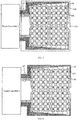
FIG. 1 is a structural schematic diagram of a sensing electrode of a capacitive hover touch sensor in the existing technology; -
FIG. 2 is a schematic side diagram of a capacitive hover touch sensor according to a first embodiment of the present disclosure; -
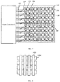
FIG. 3 is a structural schematic diagram of the capacitive hover touch sensor and sub-regions of the capacitive hover touch sensor according to the first embodiment of the present disclosure; -
FIG. 4 is a structural schematic diagram of a bridge connection of the capacitive hover touch sensor according to the first embodiment of the present disclosure; -
FIG. 5 is a schematic diagram of a connection between a strip electrode of the capacitive hover touch sensor including a shield layer and a touch controller according to the first embodiment of the present invention; -
FIG. 6 is a schematic diagram of a connection between the strip electrode of the capacitive hover touch sensor not including the shield layer and the touch controller according to the first embodiment of the present invention; -
FIG. 7 is a structural schematic diagram of strip electrodes of the capacitive hover touch sensor being connected to the touch controller by a trace layer according to a second embodiment of the present disclosure; -
FIG. 8 is a schematic diagram of a strip electrode arrangement in a sub-region of the capacitive hover touch sensor according to a third embodiment of the present disclosure; -
FIG. 9 is a schematic side diagram of the capacitive hover touch sensor according to the third embodiment of the present disclosure; -
FIG. 10 is a structural schematic diagram of a connection between strip electrodes of the capacitive hover touch sensor including a shield layer and a touch controller according to the third embodiment of the present disclosure; -
FIG. 11 is a structural schematic diagram of a connection between the strip electrodes of the capacitive hover touch sensor not including the shield layer and the touch controller according to the third embodiment of the present disclosure; -
FIG. 12 is a schematic side diagram of a capacitive hover touch sensor according to a fourth embodiment of the present disclosure; -
FIG. 13 is a structural schematic diagram of a connection between strip electrodes of the capacitive hover touch sensor including a shield layer and a touch controller by a trace layer according to the fourth embodiment of the present disclosure; -
FIG. 14 is a structural schematic diagram of a connection between the strip electrodes of the capacitive hover touch sensor not including the shield layer and the touch controller by a trace layer according to the second embodiment of the present disclosure. - The embodiments of the present disclosure will be described in detail below with reference to the accompanying drawings in order to make the objectives, technical solutions and advantages of the present invention clearer. However, it will be apparent to those skilled in the art that, in the various embodiments of the present invention, numerous technical details are set forth in order to provide the reader with a better understanding of the present disclosure. However, the technical solutions claimed in the present disclosure can be implemented without these technical details and various changes and modifications based on the following embodiments.
- It shall be noted that the words "upper", "lower", "left", "right" and the like described in the embodiments of the present disclosure are described based on the drawings, and shall not be perceived as a limitation to the embodiments of the present disclosure. In addition, in the context, it shall also be perceived that when an element is referred to as "on" or "under" another element, it may be formed "on" or "under" the other element directly or indirectly through an intermediate element.
- In a current multi hover touch solution in this industry, a two-dimensional lattice array arrangement as shown in
FIG. 1 is generally adopted for sensing electrodes, and an individual sensing electrode is a rectangular graphic with a width of L and a height of D as shown inFIG. 1 . - The inventors find that at least the following problems exist in the existing technology: in the multi hover touch device shown in
FIG. 1 , each rectangular sensing electrode (corresponding to one touch detection point) is connected to a touch controller by a wire, that is, each touch detection point corresponds to an individually configured capacitive detection channel. Therefore, in a case where higher touch recognition accuracy is required, the number of capacitive detection channels increases greatly, resulting in a large increase in manufacturing difficulty and cost. - In view of the above, a first embodiment of the present disclosure relates to a capacitive hover touch sensor, which may be applied to, but not limited to, an electronic equipment such as a smart phone, a tablet computer, a laptop, or the like. The capacitive hover touch sensor of the present embodiment includes an electrode pattern layer where a touch region is formed. The touch region is divided into P sub-regions, the number of which may be determined by area of the touch region and touch detection performance. The larger the touch region is, the larger the number of the sub-regions is; the smaller the touch region is, the smaller the number of the sub-regions is. Each of the sub-regions is respectively provided with a plurality of first strip electrodes and a plurality of second strip electrodes. The plurality of first strip electrodes and the plurality of second strip electrodes are respectively connected to a touch controller by wires. Herein, the plurality of first strip electrodes are in a one-dimensional array, the plurality of second strip electrodes are in a one-dimensional array, and the plurality of first strip electrodes are interdigitated with the plurality of second strip electrodes. For example, the plurality of first strip electrodes in each sub-region are in a row array, and the plurality of second strip electrodes are in a column array, interdigitating to form a plurality of intersection points. The touch controller may use the intersection points between the first strip electrodes and the second strip electrodes in each sub-region to perform touch position recognition. Each intersection point has a same touch position recognition function with an individual sensing electrode of individually arranged two-dimensional lattice sensing electrodes in the existing technology. That is, capacitive detection channels of the same number as the sum of the number of the first strip electrodes and the number of the second strip electrodes are adopted to realize a touch position detection accuracy equivalent to the touch position detection accuracy realized by capacitive detection channels of the same number as the sum of the intersection points of the same number of the first strip electrodes and the second strip electrodes. Since the sum of the number of the first strip electrodes and the number of the second strip electrodes in each sub-region is smaller than the sum of the intersection points, in this embodiment, the number of wires between the sensing electrodes (i.e., the first strip electrodes and the second strip electrodes) and the touch controller, the number of capacitive detection channels and the number of pins of the touch controller may be reduced, so that difficulty in design and manufacturing and cost of production may be reduced.
- Specifically, an
electrode pattern layer 101 in this embodiment is of a single-layer structure. With reference toFIG. 2 , the capacitive hover touch sensor in this embodiment further includes abridge layer 102 disposed in a stack with theelectrode pattern layer 101, and ashield layer 103; theshield layer 103, thebridge layer 102 and theelectrode pattern layer 101 are disposed in a stack one by one bottom up. With reference toFIG. 3 to FIG. 5 , both the first strip electrodes and the second strip electrodes are located in theelectrode pattern layer 101 of the single-layer structure. Each of thefirst strip electrodes 104 and each of thesecond strip electrodes 105 respectively comprise a plurality of electrode patterns. A plurality of electrode patterns of thefirst strip electrodes 104 are connected in series. A plurality of electrode patterns of thesecond strip electrodes 105 are connected in series. The electrode patterns of the plurality offirst strip electrodes 104 interdigitate with the electrode patterns of the plurality ofsecond strip electrodes 105. The electrode patterns of either thefirst strip electrodes 104 or thesecond strip electrodes 105 at intersection points are bridged by thebridge layer 102. For example, thefirst strip electrodes 104 form row electrodes of asub-region 10 and thesecond strip electrodes 101 form column electrodes of thesub-region 10, to which the present disclosure is not limited, but the first strip electrodes and the second strip electrodes may not be perpendicular otherwise. - The plurality of electrode patterns of each of the
first strip electrodes 104, for example, are respectively triangular electrode patterns located at both ends of thefirst strip electrode 104 and a plurality of rhombic electrode patterns located between the triangular electrode patterns, and two triangular electrode patterns of anyfirst strip electrode 104 respectively have one vertex toward the center of thefirst strip electrode 104. Similarly, the plurality of electrode patterns of each of thesecond strip electrodes 105 are respectively triangular electrode patterns located at both ends of thesecond strip electrode 105 and a plurality of rhombic electrode patterns located between the triangular electrode patterns, and two triangular electrode patterns of any second strip electrode respectively have one vertex toward the center of thesecond strip electrode 105. In other words, both ends of anyfirst strip electrode 104 and both ends of anysecond strip electrode 105 is one side of a triangular electrode pattern thereof. The side may be perpendicular to thefirst strip electrode 104 and thesecond strip electrode 105, so that electrode patterns of thefirst strip electrode 104 andsecond strip electrode 105 form a rectangular orsquare sub-region 10, facilitating fabrication of the electrode pattern. Both thefirst strip electrode 104 and thesecond strip electrode 105 are of rhombic electrode patterns, facilitating cross-over arrangement of thefirst strip electrode 104 andsecond strip electrode 105 that take generally the same areas. In practical applications, a first strip electrode and a second strip electrode may otherwise be of a polygonal electrode pattern such as of a hexagon or an octagon, to which the present disclosure is not specifically limited in this embodiment. - In this embodiment, the
bridge layer 102 is stacked under theelectrode pattern layer 101. With further reference toFIG. 4 , at intersection points of electrode patterns of thefirst strip electrodes 104 and thesecond strip electrodes 105, a plurality of electrode patterns of thesecond strip electrodes 105 are directly interconnected in theelectrode pattern layer 101, and a plurality of electrode patterns of thefirst strip electrodes 104 are bridged by thebridge layer 102, to which the present disclosure is not limited. In some other examples, the plurality of electrode patterns of the first strip electrodes may be directly interconnected in the electrode pattern layer, and the plurality of electrode patterns of the second strip electrodes may be bridged by the bridge layer. Electrode patterns that are bridged are disconnected at intersection points, the bridge layer has vias at the disconnections of the electrode patterns, and a conductive structure is formed between the via and the bridge layer, so that an electrical connection between electrode patterns at intersection points is realized. It shall be understood that any manner that may realize bridging falls into the protection scope of this embodiment. - It shall be noted that, in this embodiment, each strip electrode, that is, all of the
first strip electrodes 104 and all of thesecond strip electrodes 105 are connected to atouch controller 2 bywires 107 on theelectrode pattern layer 101. Herein, a plurality of adjacent sub-regions, for example, four adjacent sub-regions, may be combined into a larger sub-region, and wires of the strip electrodes in the larger sub-region may be disposed around the larger sub-region, facilitating fabrication of electrode patterns and wires. - It is worth mentioning that, in the present embodiment, the
shield layer 103 for providing shielding protection for theelectrode pattern layer 101 is disposed under thebridge layer 102, and theshield layer 103 may be a grounding metal layer, so as to shield electromagnetic interference, to which the present disclosure is not limited. In some examples, with reference toFIG. 6 , the shield layer may be omitted according to application requirements and practical conditions. - In this embodiment, the multi touch is realized by a cross-over arrangement of strip electrodes. Each strip electrode (the
first strip electrode 104 or the second strip electrode 105) may only support one finger's hover touch. The cross-over arrangement of the plurality of strip electrodes may result in a plurality of intersection points, each of which may realize hover touch. It is described in the following the manner in which the multi hover touch is implemented by the strip electrodes as follows. - Herein, the number of the first strip electrodes is denoted as M, the number of the second strip electrodes is denoted as N, which interdigitate to obtain M∗N intersection points (i.e. number of touch points). That M=4 and N=4, i.e., each sub-region includes four
first strip electrodes 104 and foursecond strip electrodes 105, is taken as an example, and that 512 detection channels are required as an example. The entire touch region is divided into 32 sub-regions each including M+N (i.e., 8) strip electrodes, and then each sub-region may support 4∗4 (i.e., 16) touch points. Therefore, in this embodiment, in a case where 512 touch points are supported, only 32∗8 (i.e., 256) detection channels are required as 50% less than current 512 channels, that is, 256 detection channels are reduced. Correspondingly, wires between the strip electrodes and thetouch controller 2 are reduced by half, and the number of pins of thetouch controller 2 is reduced by half, which may significantly reduce difficulty in fabrication of the wires and pins of the touch controller. In some examples, the number of the first strip electrodes and second strip electrodes in each sub-region may be varied, for example, the number may be set as, but not limited to, eight. The more the number of the cross-over arranged strip electrodes in each sub-region, the smaller the number of detection channels required for the capacitive hover touch sensor. For the sake of simple design, a width L and a height D of the first strip electrodes and second strip electrodes may be equal. - Compared with the existing technology, by disposing interdigitating strip electrodes in the electrode pattern layer, this embodiment may use the interdigitating strip electrodes to realize multi hover, which solves the problems of difficulty in design and fabrication and high cost due to too large numbers of detection channels, wires and pins of the touch controller resulted from multi hover by directly using individual capacitive detection channels.
- A second embodiment of the present disclosure relates to a capacitive hover touch sensor, which is generally the same as the first embodiment, but mainly different in: in the first embodiment, all the strip electrodes are connected to the touch controller by wires in the electrode pattern layer; while in the second embodiment, all the strip electrodes are connected to the touch controller by wires in the trace layer, so that the wires for the strip electrodes may be prevented from occupying the areas of the electrode patterns, which facilitates improving touch sensitivity.
- With reference to
FIG. 2 andFIG. 7 , in this embodiment, the capacitive hover touch sensor further includes a trace layer disposed in a stack with theelectrode pattern layer 101. In this case, thebridge layer 102 in the first embodiment may be reused as the trace layer, to which the present disclosure is not limited. An individual trace layer 111 (seeFig. 12 ) may be used and disposed in a stack under the bridge layer.First vias 108 are formed in the electrode patterns of thefirst strip electrodes 104 and thesecond strip electrodes 105, andsecond vias 109 are formed in theelectrode pattern layer 101. Thefirst vias 108 and thesecond vias 109 are electrically connected bywires 110 in the trace layer, and thesecond vias 109 are connected to thetouch controller 102 bywires 107 on theelectrode pattern layer 101, so that thefirst strip electrodes 104 and thesecond strip electrodes 105 are electrically connected to thetouch controller 2. Specifically, the plurality ofsecond vias 109 may be in an array, and the plurality offirst vias 108 may also be in an array. Herein, thefirst vias 108 of thefirst strip electrodes 104 in each sub-region may be arranged in a row on the rhombic electrode pattern, and thefirst vias 108 of thesecond strip electrodes 105 may be arranged in a generally equidistant manner in a direction of extension of thesecond strip electrodes 105, thereby facilitating fabrication of thefirst vias 108 and thesecond vias 109. In order to avoid short circuits, the wires in the trace layer need to bypass a bridge region. In this embodiment, by moving wires that connect thefirst strip electrodes 104 to thetouch controller 2 and thesecond strip electrodes 105 to thetouch controller 2 to the trace layer, the wires of the strip electrodes may be prevented from occupying too much area of theelectrode pattern layer 101, which further facilitates increasing area taken by the electrode patterns and improving sensitivity of hover touch. In this embodiment, the trace layer is interconnected through the second vias to theelectrode pattern layer 101 to realize interconnection between the strip electrodes and thetouch controller 2, to which the present disclosure is not limited, for example, electrodes in theelectrode pattern layer 101 may be interconnected with the touch controller through other layers of the capacitive hover touch sensor. In some examples, some of the first strip electrodes and second strip electrodes may be interconnected with thetouch controller 2 through the trace layer, or either the first strip electrodes or the second strip electrodes may be interconnected with thetouch controller 2 through the trace layer. - It shall be noted that the capacitive hover touch sensor in this embodiment includes the
shield layer 103 disposed in a stack under thebridge layer 102. In some examples, the shield layer may also be omitted. - Compared with the above-described embodiments, by moving wires of the stipe electrodes to the
bridge layer 102 or an individual trace layer, area of the electrode patterns may be increased and difficulty in fabrication of wires may be reduced. - A third embodiment of the present disclosure relates to a capacitive hover touch sensor, which is generally the same as the first embodiment, but mainly different in: in the first embodiment, the electrode pattern layer is of a single-layer structure, the electrode patterns of the strip electrodes need to be bridged by the bridge layer, while in the third embodiment, the electrode pattern layer is of a double-layer structure and thus there is no need to adopt bridging, facilitating simplification of production process.
- With reference to
FIGs. 8-11 , in this embodiment, theelectrode pattern layer 101 is of a double-layer structure, and the plurality offirst strip electrodes 104 are located in one layer of the double-layer structure, and the plurality ofsecond strip electrodes 105 are located in the other layer of the double-layer structure. Specifically, theelectrode pattern layer 101 includes afirst sub-layer 1011 and asecond sub-layer 1012 which are disposed in a stack, and thefirst sub-layer 1011 is located over thesecond sub-layer 1012. The plurality offirst strip electrodes 104 are disposed in the second sub-layer 1012 (i.e., the lower layer of the electrode pattern layer 101), and the plurality ofsecond strip electrodes 105 are disposed in the first sub-layer 1011 (i.e., the upper layer of the electrode pattern layer 101). For example, all of thefirst strip electrodes 104 and all of thesecond strip electrodes 105 are of rectangular electrode patterns, and the area of any upper-layer electrode pattern in the two-layer structure is smaller than the area of any lower-layer electrode pattern. Specifically, afirst strip electrode 104 is, for example, a rectangular strip electrode having a length more than five times of its width, and asecond strip electrode 105 is, for example, a rectangular strip electrode having a length more than eight times of its width. In this way, electrode patterns of thefirst sub-layer 1011 which is the upper layer of theelectrode pattern layer 101 are narrower, so electrode patterns on thesecond sub-layer 1012 which is the lower layer may be exposed, so that sensing sensitivity of the electrode patterns on thesecond sub-layer 1012 is higher, to which the present disclosure is not limited, but in some examples, forms and sizes of thefirst strip electrodes 104 andsecond strip electrodes 105 may be adjusted. - It shall be noted that, in this embodiment, the strip electrodes (i.e., the
first strip electrodes 104 and the second strip electrodes 105) are connected to thetouch controller 2 bywires 107 on the electrode pattern layer, to which the present disclosure is not limited. - It shall be noted that, in this embodiment, the capacitive hover touch sensor further includes a
shield layer 103 disposed in a stack under theelectrode pattern layer 101. In some examples, the shield layer may be omitted. - Compared with the above-described embodiments, this embodiment provides a double-layer electrode pattern layer, thereby eliminating the need for a bridging process, which is advantageous for simplifying the fabrication process.
- A fourth embodiment of the present disclosure relates to a capacitive hover touch sensor, which is generally the same as the second embodiment, but mainly different in: in the second embodiment, the electrode pattern layer is of a single-layer structure, and the plurality of electrode patterns of the strip electrodes need to be bridged by the bridge layer; while in the fourth embodiment, the electrode pattern layer is of a double-layer structure, so no bridge process is needed, which is advantageous for simplifying production process.
- With reference to
FIG. 12 to FIG. 14 , the capacitive hover touch sensor includes anelectrode pattern layer 101, atrace layer 111, and ashield layer 103 which are disposed in a stack one by one top down.First vias 108 are formed in the electrode patterns of thefirst strip electrodes 104 and thesecond strip electrodes 105, andsecond vias 109 are formed in theelectrode pattern layer 101; thefirst vias 108 and thesecond vias 109 are electrically connected bywires 110 in thetrace layer 111, and thesecond vias 109 are connected to thetouch controller 2 bywires 107 on theelectrode pattern layer 101, so that thefirst strip electrodes 104 and thesecond strip electrodes 105 are electrically connected to thetouch controller 2. Specifically, the plurality ofsecond vias 109 may be in an array, and the plurality offirst vias 108 may also be in an array. Herein, thefirst vias 108 of anyfirst strip electrode 104 in each sub-region may be arranged in a row and on the rectangular electrode patterns, and thefirst vias 108 of anysecond strip electrode 105 may be disposed in a generally equidistant manner in the extending direction of thesecond strip electrodes 105, thereby facilitating fabrication of thefirst vias 108 and thesecond vias 109. In this embodiment, by moving wires that connect thefirst strip electrodes 104 to thetouch controller 2 and thesecond strip electrodes 105 to thetouch controller 2 to thetrace layer 111, the wires of the strip electrodes may be prevented from occupying too much area of theelectrode pattern layer 101, which further facilitates increasing area taken by the electrode patterns and improving sensitivity of hover touch. In this embodiment, thetrace layer 111 is interconnected through thesecond vias 109 to theelectrode pattern layer 101 to realize interconnection between the strip electrodes and thetouch controller 2, to which the present disclosure is not limited, for example, electrodes in theelectrode pattern layer 101 may be interconnected with thetouch controller 2 through other layers of the capacitive hover touch sensor. In some examples, some of the first strip electrodes and second strip electrodes may be interconnected with thetouch controller 2 through the trace layer, or either thefirst strip electrodes 104 or thesecond strip electrodes 105 may be interconnected with thetouch controller 2 through the trace layer. - It shall be noted that, in this embodiment, the
shield layer 103 is disposed in a stack under thetrace layer 111. In some examples, the shield layer may be omitted. - Compared with the above-described embodiments, by moving wires of the stipe electrodes to the trace layer, area of the electrode patterns may be increased, difficulty in fabrication of wires may be reduced, and sensitivity of hover touch may be improved.
- A fifth embodiment of the present disclosure relates to a capacitive hover touch device that may be applied to an electronic equipment such as a smart phone, a tablet computer, a laptop, or the like. With further reference to
FIGs. 5 ,11 , and13 , the capacitive hover touch device in the present embodiment includes thetouch controller 2 and the capacitive hover touch sensor as described in the above embodiments, and the capacitive hover touch sensor is connected to the touch controller. - Compared with the existing technology, by using a cross-over arrangement of strip electrodes to realize multi hover, this embodiment solves the problems of difficulty in design and fabrication and high cost due to too large numbers of capacitance detection channels, wires and pins of touch controller resulted from multi hover by directly using individual capacitive detection channels.
- A sixth embodiment of the present disclosure relates to an electronic equipment, for example, an electronic equipment such as a smartphone, a tablet computer, a laptop, or the like. The electronic equipment includes the capacitive hover touch device as described in the fifth embodiment. The capacitive hover touch device may be integrated into the display of the electronic equipment. The display screen of the electronic equipment may be a hard screen or a flexible screen.
- Compared with the existing technology, by using a cross-over arrangement of strip electrodes to realize multi hover, this embodiment solves the problems of difficulty in design and fabrication and high cost due to too large numbers of detection channels, wires and pins of touch controller resulted from multi hover by directly using individual capacitive detection channels.
- Those skilled in the art shall appreciate that the aforementioned embodiments are specific embodiments for implementing the present invention. In practice, however, many changes can be made in the forms and details of the specific embodiments without departing from the scope of the invention.
Claims (11)
- A capacitive hover touch sensor, characterized by comprising: an electrode pattern layer (101) that formed a touch region; wherein
the touch region is divided into P sub-regions (10), P being a natural number greater than 1;
each of the sub-regions (10) is provided with a plurality of first strip electrodes (104) in a one-dimensional array and a plurality of second strip electrodes (105) in a one-dimensional array;the plurality of first strip electrodes (104) are interdigitated with the plurality of second strip electrodes (105); andthe plurality of first strip electrodes (104) in each of the sub-regions and the plurality of second strip electrodes (105) in each of the sub-regions (10) are respectively connected to a touch controller (2) by wires (107). - The capacitive hover touch sensor according to claim 1, wherein the electrode pattern layer (101) is of a single-layer structure, and the capacitive hover touch sensor further comprises a bridge layer (102) disposed in a stack with the electrode pattern layer (101);
wherein the plurality of first strip electrodes (104) and the plurality of second strip electrodes (105) are located in the electrode pattern layer (101) of the single-layer structure;
wherein each of the plurality of first strip electrodes (104) and each of the second strip electrodes (105) respectively comprise a plurality of electrode patterns, the plurality of electrode patterns of the first strip electrodes (104) are connected in series, and the plurality of electrode patterns of the second strip electrodes (105) are connected in series; and
wherein the electrode patterns of the plurality of first strip electrodes (104) are interdigitated with the electrode patterns of the plurality of second strip electrodes (105), and wherein the electrode patterns of either the first strip electrodes (104) or the second strip electrodes (105) at intersection points are bridged connected by the bridge layer (102). - The capacitive hover touch sensor according to claim 2, wherein the plurality of electrode patterns of each of the plurality of first strip electrodes (104) are triangular electrode patterns located at both ends of the first strip electrodes (104) and a plurality of rhombic electrode patterns located between the triangular electrode patterns, and wherein two triangular electrode patterns of any first strip electrode (104) respectively have one vertex toward the center of the first strip electrode; and
wherein the plurality of electrode patterns of each of the plurality of second strip electrodes (105) are triangular electrode patterns located at both ends of the second strip electrodes (105) and a plurality of rhombic electrode patterns located between the triangular electrode patterns, and wherein two triangular electrode patterns of any second strip electrode (105) respectively have one vertex toward the center of the second strip electrode. - The capacitive hover touch sensor according to claim 1, wherein the electrode pattern layer (101) is of a double-layer structure; and
wherein the plurality of first strip electrodes (104) are located in one layer of the double-layer structure, and the plurality of second strip electrodes (105) are located in the other layer of the double-layer structure. - The capacitive hover touch sensor according to claim 4, wherein the plurality of first strip electrodes (104) and the plurality of second strip electrodes (105) are of rectangular electrode patterns, and an area of electrode patterns of an upper layer in the double-layer structure is smaller than an area of electrode patterns of a lower layer.
- The capacitive hover touch sensor according to any one of claims 2 to 5, further comprising a trace layer (111) disposed in a stack with the electrode pattern layer (101);
wherein first vias are formed in the electrode patterns of the first strip electrodes (104) and the second strip electrodes (105), and second vias are formed in the electrode pattern layer (101); the first vias and the second vias are electrically connected by wires (107) in the trace layer (111), and the second vias are connected to the touch controller (2) by wires (107) on the electrode pattern layer (101). - The capacitive hover touch sensor according to any one of claims 2 to 5, further comprising a trace layer (111) disposed in a stack with the electrode pattern layer (101);
wherein first vias are formed in the electrode patterns of the first strip electrodes (104) or the second strip electrodes (105), and second vias are formed in the electrode pattern layer (101); the first vias and the second vias are electrically connected by wires (107) in the trace layer (111), and the second vias are connected to the touch controller (2) by wires (107) on the electrode pattern layer (101). - The capacitive hover touch sensor according to any one of claims 1 to 7, further comprising a shield layer (103) for providing shielding protection for the electrode pattern layer (101).
- The capacitive hover touch sensor according to any one of claims 1 to 8, wherein each of the sub-regions (10) comprises four first strip electrodes (104) and four second strip electrodes (105).
- A capacitive hover touch device, comprising a touch controller (2) and the capacitive hover touch sensor according to any one of claims 1 to 9;
wherein the capacitive hover touch sensor is connected to the touch controller (2). - An electronic equipment, comprising the capacitive hover touch device according to claim 10.
Applications Claiming Priority (1)
| Application Number | Priority Date | Filing Date | Title |
|---|---|---|---|
| CN201821406294.8U CN208673308U (en) | 2018-08-29 | 2018-08-29 | Condenser type suspension touch control sensor, device and electronic equipment |
Publications (2)
| Publication Number | Publication Date |
|---|---|
| EP3617859A1 true EP3617859A1 (en) | 2020-03-04 |
| EP3617859B1 EP3617859B1 (en) | 2021-11-17 |
Family
ID=65839973
Family Applications (1)
| Application Number | Title | Priority Date | Filing Date |
|---|---|---|---|
| EP19182159.4A Active EP3617859B1 (en) | 2018-08-29 | 2019-06-25 | Capacitive hover touch sensor, device, and electronic equipment |
Country Status (3)
| Country | Link |
|---|---|
| US (1) | US11182035B2 (en) |
| EP (1) | EP3617859B1 (en) |
| CN (1) | CN208673308U (en) |
Families Citing this family (10)
| Publication number | Priority date | Publication date | Assignee | Title |
|---|---|---|---|---|
| US10921854B2 (en) * | 2018-09-06 | 2021-02-16 | Apple Inc. | Electronic device with sensing strip |
| US11249587B2 (en) * | 2019-04-10 | 2022-02-15 | Himax Technologies Limited | Touch panel and touch display apparatus |
| KR102883316B1 (en) | 2019-10-16 | 2025-11-10 | 삼성디스플레이 주식회사 | Touch sensor and display device having the same |
| BR112023017828A2 (en) | 2021-03-03 | 2023-10-03 | Guardian Glass Llc | SYSTEMS AND/OR METHODS FOR CREATING AND DETECTING CHANGES IN ELECTRIC FIELDS |
| CN113467639B (en) | 2021-06-30 | 2023-05-23 | 合肥维信诺科技有限公司 | Touch panel and touch display device |
| US12026317B2 (en) | 2021-09-16 | 2024-07-02 | Apple Inc. | Electronic devices with air input sensors |
| KR20230139932A (en) * | 2022-03-28 | 2023-10-06 | 삼성디스플레이 주식회사 | Display device |
| EP4422376A4 (en) | 2022-04-26 | 2024-10-30 | BOE Technology Group Co., Ltd. | DISPLAY DEVICE AND TOUCH DISPLAY PANEL AND CONTROL METHOD THEREFOR |
| TWI843411B (en) * | 2023-01-18 | 2024-05-21 | 元太科技工業股份有限公司 | Touch panel and sensing display device |
| CN119311154A (en) * | 2024-09-29 | 2025-01-14 | 深圳市芯璨科技有限公司 | A high-precision touch electrode for touch panels |
Citations (3)
| Publication number | Priority date | Publication date | Assignee | Title |
|---|---|---|---|---|
| US20110141040A1 (en) * | 2009-12-11 | 2011-06-16 | Hee-Kwang Kang | Touch panel and liquid crystal display device including the same |
| KR101658139B1 (en) * | 2009-10-15 | 2016-09-20 | 엘지디스플레이 주식회사 | Touch Panel |
| CN108153445A (en) * | 2017-11-30 | 2018-06-12 | 云谷(固安)科技有限公司 | A kind of touch-control display panel and touch control display apparatus |
Family Cites Families (13)
| Publication number | Priority date | Publication date | Assignee | Title |
|---|---|---|---|---|
| US20130176262A1 (en) * | 2012-01-05 | 2013-07-11 | Silicon Integrated Systems Corp. | Projected capacitive touch panel |
| JP2014206936A (en) * | 2013-04-15 | 2014-10-30 | 富士フイルム株式会社 | Method of manufacturing conductive sheet for touch panel, and conductive sheet for touch panel |
| CN103472963B (en) * | 2013-09-06 | 2016-05-11 | 北京京东方光电科技有限公司 | A kind of touching display screen and touch control display apparatus |
| KR102092569B1 (en) * | 2013-09-17 | 2020-03-25 | 엘지디스플레이 주식회사 | Display Device Integrated With Touch Screen and Method for Driving The Same |
| US10168732B2 (en) * | 2014-02-27 | 2019-01-01 | Industrial Technology Research Institute | Touch panel and sensing method thereof |
| KR102489827B1 (en) * | 2015-12-31 | 2023-01-17 | 엘지디스플레이 주식회사 | Display device |
| JP6637344B2 (en) * | 2016-03-09 | 2020-01-29 | 株式会社ジャパンディスプレイ | Detection device, display device and electronic equipment |
| US10416821B2 (en) * | 2016-07-04 | 2019-09-17 | Boe Technology Group Co., Ltd. | Touch substrate, touch display panel and touch display apparatus having the same, and fabricating method thereof |
| CN106445230A (en) * | 2016-09-12 | 2017-02-22 | 京东方科技集团股份有限公司 | Touch panel and manufacturing method thereof and display device |
| CN107357475B (en) * | 2017-06-27 | 2020-12-29 | 上海天马微电子有限公司 | Touch panel and display device |
| KR102427667B1 (en) * | 2017-09-26 | 2022-08-02 | 삼성디스플레이 주식회사 | Display apparatus |
| CN107656646A (en) * | 2017-09-27 | 2018-02-02 | 上海天马微电子有限公司 | Touch sensor and touch display panel |
| CN108710447A (en) * | 2018-05-14 | 2018-10-26 | 京东方科技集团股份有限公司 | A kind of touch-control structure and display screen |
-
2018
- 2018-08-29 CN CN201821406294.8U patent/CN208673308U/en active Active
-
2019
- 2019-06-25 EP EP19182159.4A patent/EP3617859B1/en active Active
- 2019-06-27 US US16/455,691 patent/US11182035B2/en active Active
Patent Citations (4)
| Publication number | Priority date | Publication date | Assignee | Title |
|---|---|---|---|---|
| KR101658139B1 (en) * | 2009-10-15 | 2016-09-20 | 엘지디스플레이 주식회사 | Touch Panel |
| US20110141040A1 (en) * | 2009-12-11 | 2011-06-16 | Hee-Kwang Kang | Touch panel and liquid crystal display device including the same |
| CN108153445A (en) * | 2017-11-30 | 2018-06-12 | 云谷(固安)科技有限公司 | A kind of touch-control display panel and touch control display apparatus |
| US20190265827A1 (en) * | 2017-11-30 | 2019-08-29 | Yungu (Gu'an) Technology Co., Ltd. | Touch display panel and touch display device |
Also Published As
| Publication number | Publication date |
|---|---|
| US11182035B2 (en) | 2021-11-23 |
| US20200073512A1 (en) | 2020-03-05 |
| CN208673308U (en) | 2019-03-29 |
| EP3617859B1 (en) | 2021-11-17 |
Similar Documents
| Publication | Publication Date | Title |
|---|---|---|
| US11182035B2 (en) | Capacitive hover touch sensor, device, and electronic equipment | |
| US9329742B2 (en) | Capacitive touch panel | |
| US9952733B2 (en) | Touch screen panel having a plurality of openings in a plurality of sensing cells | |
| KR101323004B1 (en) | Capacity type touch screen panel | |
| CN108700971B (en) | Touch Panels and Display Units | |
| KR101093326B1 (en) | Touch screen panel and its manufacturing method | |
| CN103995616B (en) | Embedded touch panel and display device | |
| KR101471753B1 (en) | Touch sensing electrode structure | |
| EP3951565B1 (en) | Touch screen, touch display screen, and display apparatus | |
| KR101850636B1 (en) | Conductive sheet, capacitive touch panel, and display device | |
| KR101814656B1 (en) | Electronic device and single-layer mutual-capacitance touch screen thereof | |
| CN112673337B (en) | Touch panel and touch display panel | |
| US9811230B2 (en) | Touch panel and production method thereof | |
| US9519383B2 (en) | ITO pattern for capacitive touchscreen applications | |
| TW201635107A (en) | Touch device | |
| CN114115613B (en) | Touch screen, touch positioning method and display device | |
| CN109976569B (en) | Touch panel and preparation method thereof, and touch device | |
| KR20220065836A (en) | touch panel | |
| CN111367438A (en) | Display panel and display device | |
| US10782840B1 (en) | Touch panel | |
| CN105027050B (en) | Capacitive sensor electrodes | |
| CN203858607U (en) | Embedded touch panel and display device | |
| US20110084920A1 (en) | Reducing layers in a touchpad by maximizing distance between a ground plane and sensor electrodes electrodes | |
| CN120066319A (en) | Touch control device | |
| CN206224430U (en) | Touch induction device |
Legal Events
| Date | Code | Title | Description |
|---|---|---|---|
| PUAI | Public reference made under article 153(3) epc to a published international application that has entered the european phase |
Free format text: ORIGINAL CODE: 0009012 |
|
| STAA | Information on the status of an ep patent application or granted ep patent |
Free format text: STATUS: REQUEST FOR EXAMINATION WAS MADE |
|
| 17P | Request for examination filed |
Effective date: 20190625 |
|
| AK | Designated contracting states |
Kind code of ref document: A1 Designated state(s): AL AT BE BG CH CY CZ DE DK EE ES FI FR GB GR HR HU IE IS IT LI LT LU LV MC MK MT NL NO PL PT RO RS SE SI SK SM TR |
|
| AX | Request for extension of the european patent |
Extension state: BA ME |
|
| STAA | Information on the status of an ep patent application or granted ep patent |
Free format text: STATUS: EXAMINATION IS IN PROGRESS |
|
| 17Q | First examination report despatched |
Effective date: 20210126 |
|
| GRAP | Despatch of communication of intention to grant a patent |
Free format text: ORIGINAL CODE: EPIDOSNIGR1 |
|
| STAA | Information on the status of an ep patent application or granted ep patent |
Free format text: STATUS: GRANT OF PATENT IS INTENDED |
|
| INTG | Intention to grant announced |
Effective date: 20210901 |
|
| GRAS | Grant fee paid |
Free format text: ORIGINAL CODE: EPIDOSNIGR3 |
|
| GRAA | (expected) grant |
Free format text: ORIGINAL CODE: 0009210 |
|
| STAA | Information on the status of an ep patent application or granted ep patent |
Free format text: STATUS: THE PATENT HAS BEEN GRANTED |
|
| AK | Designated contracting states |
Kind code of ref document: B1 Designated state(s): AL AT BE BG CH CY CZ DE DK EE ES FI FR GB GR HR HU IE IS IT LI LT LU LV MC MK MT NL NO PL PT RO RS SE SI SK SM TR |
|
| REG | Reference to a national code |
Ref country code: GB Ref legal event code: FG4D |
|
| REG | Reference to a national code |
Ref country code: DE Ref legal event code: R096 Ref document number: 602019009303 Country of ref document: DE |
|
| REG | Reference to a national code |
Ref country code: IE Ref legal event code: FG4D |
|
| REG | Reference to a national code |
Ref country code: AT Ref legal event code: REF Ref document number: 1448605 Country of ref document: AT Kind code of ref document: T Effective date: 20211215 |
|
| REG | Reference to a national code |
Ref country code: LT Ref legal event code: MG9D |
|
| REG | Reference to a national code |
Ref country code: NL Ref legal event code: MP Effective date: 20211117 |
|
| REG | Reference to a national code |
Ref country code: AT Ref legal event code: MK05 Ref document number: 1448605 Country of ref document: AT Kind code of ref document: T Effective date: 20211117 |
|
| PG25 | Lapsed in a contracting state [announced via postgrant information from national office to epo] |
Ref country code: RS Free format text: LAPSE BECAUSE OF FAILURE TO SUBMIT A TRANSLATION OF THE DESCRIPTION OR TO PAY THE FEE WITHIN THE PRESCRIBED TIME-LIMIT Effective date: 20211117 Ref country code: LT Free format text: LAPSE BECAUSE OF FAILURE TO SUBMIT A TRANSLATION OF THE DESCRIPTION OR TO PAY THE FEE WITHIN THE PRESCRIBED TIME-LIMIT Effective date: 20211117 Ref country code: FI Free format text: LAPSE BECAUSE OF FAILURE TO SUBMIT A TRANSLATION OF THE DESCRIPTION OR TO PAY THE FEE WITHIN THE PRESCRIBED TIME-LIMIT Effective date: 20211117 Ref country code: BG Free format text: LAPSE BECAUSE OF FAILURE TO SUBMIT A TRANSLATION OF THE DESCRIPTION OR TO PAY THE FEE WITHIN THE PRESCRIBED TIME-LIMIT Effective date: 20220217 Ref country code: AT Free format text: LAPSE BECAUSE OF FAILURE TO SUBMIT A TRANSLATION OF THE DESCRIPTION OR TO PAY THE FEE WITHIN THE PRESCRIBED TIME-LIMIT Effective date: 20211117 |
|
| PG25 | Lapsed in a contracting state [announced via postgrant information from national office to epo] |
Ref country code: IS Free format text: LAPSE BECAUSE OF FAILURE TO SUBMIT A TRANSLATION OF THE DESCRIPTION OR TO PAY THE FEE WITHIN THE PRESCRIBED TIME-LIMIT Effective date: 20220317 Ref country code: SE Free format text: LAPSE BECAUSE OF FAILURE TO SUBMIT A TRANSLATION OF THE DESCRIPTION OR TO PAY THE FEE WITHIN THE PRESCRIBED TIME-LIMIT Effective date: 20211117 Ref country code: PT Free format text: LAPSE BECAUSE OF FAILURE TO SUBMIT A TRANSLATION OF THE DESCRIPTION OR TO PAY THE FEE WITHIN THE PRESCRIBED TIME-LIMIT Effective date: 20220317 Ref country code: PL Free format text: LAPSE BECAUSE OF FAILURE TO SUBMIT A TRANSLATION OF THE DESCRIPTION OR TO PAY THE FEE WITHIN THE PRESCRIBED TIME-LIMIT Effective date: 20211117 Ref country code: NO Free format text: LAPSE BECAUSE OF FAILURE TO SUBMIT A TRANSLATION OF THE DESCRIPTION OR TO PAY THE FEE WITHIN THE PRESCRIBED TIME-LIMIT Effective date: 20220217 Ref country code: NL Free format text: LAPSE BECAUSE OF FAILURE TO SUBMIT A TRANSLATION OF THE DESCRIPTION OR TO PAY THE FEE WITHIN THE PRESCRIBED TIME-LIMIT Effective date: 20211117 Ref country code: LV Free format text: LAPSE BECAUSE OF FAILURE TO SUBMIT A TRANSLATION OF THE DESCRIPTION OR TO PAY THE FEE WITHIN THE PRESCRIBED TIME-LIMIT Effective date: 20211117 Ref country code: HR Free format text: LAPSE BECAUSE OF FAILURE TO SUBMIT A TRANSLATION OF THE DESCRIPTION OR TO PAY THE FEE WITHIN THE PRESCRIBED TIME-LIMIT Effective date: 20211117 Ref country code: GR Free format text: LAPSE BECAUSE OF FAILURE TO SUBMIT A TRANSLATION OF THE DESCRIPTION OR TO PAY THE FEE WITHIN THE PRESCRIBED TIME-LIMIT Effective date: 20220218 Ref country code: ES Free format text: LAPSE BECAUSE OF FAILURE TO SUBMIT A TRANSLATION OF THE DESCRIPTION OR TO PAY THE FEE WITHIN THE PRESCRIBED TIME-LIMIT Effective date: 20211117 |
|
| PG25 | Lapsed in a contracting state [announced via postgrant information from national office to epo] |
Ref country code: SM Free format text: LAPSE BECAUSE OF FAILURE TO SUBMIT A TRANSLATION OF THE DESCRIPTION OR TO PAY THE FEE WITHIN THE PRESCRIBED TIME-LIMIT Effective date: 20211117 Ref country code: SK Free format text: LAPSE BECAUSE OF FAILURE TO SUBMIT A TRANSLATION OF THE DESCRIPTION OR TO PAY THE FEE WITHIN THE PRESCRIBED TIME-LIMIT Effective date: 20211117 Ref country code: RO Free format text: LAPSE BECAUSE OF FAILURE TO SUBMIT A TRANSLATION OF THE DESCRIPTION OR TO PAY THE FEE WITHIN THE PRESCRIBED TIME-LIMIT Effective date: 20211117 Ref country code: EE Free format text: LAPSE BECAUSE OF FAILURE TO SUBMIT A TRANSLATION OF THE DESCRIPTION OR TO PAY THE FEE WITHIN THE PRESCRIBED TIME-LIMIT Effective date: 20211117 Ref country code: DK Free format text: LAPSE BECAUSE OF FAILURE TO SUBMIT A TRANSLATION OF THE DESCRIPTION OR TO PAY THE FEE WITHIN THE PRESCRIBED TIME-LIMIT Effective date: 20211117 Ref country code: CZ Free format text: LAPSE BECAUSE OF FAILURE TO SUBMIT A TRANSLATION OF THE DESCRIPTION OR TO PAY THE FEE WITHIN THE PRESCRIBED TIME-LIMIT Effective date: 20211117 |
|
| REG | Reference to a national code |
Ref country code: DE Ref legal event code: R097 Ref document number: 602019009303 Country of ref document: DE |
|
| PLBE | No opposition filed within time limit |
Free format text: ORIGINAL CODE: 0009261 |
|
| STAA | Information on the status of an ep patent application or granted ep patent |
Free format text: STATUS: NO OPPOSITION FILED WITHIN TIME LIMIT |
|
| 26N | No opposition filed |
Effective date: 20220818 |
|
| PG25 | Lapsed in a contracting state [announced via postgrant information from national office to epo] |
Ref country code: AL Free format text: LAPSE BECAUSE OF FAILURE TO SUBMIT A TRANSLATION OF THE DESCRIPTION OR TO PAY THE FEE WITHIN THE PRESCRIBED TIME-LIMIT Effective date: 20211117 |
|
| PG25 | Lapsed in a contracting state [announced via postgrant information from national office to epo] |
Ref country code: SI Free format text: LAPSE BECAUSE OF FAILURE TO SUBMIT A TRANSLATION OF THE DESCRIPTION OR TO PAY THE FEE WITHIN THE PRESCRIBED TIME-LIMIT Effective date: 20211117 |
|
| PG25 | Lapsed in a contracting state [announced via postgrant information from national office to epo] |
Ref country code: MC Free format text: LAPSE BECAUSE OF FAILURE TO SUBMIT A TRANSLATION OF THE DESCRIPTION OR TO PAY THE FEE WITHIN THE PRESCRIBED TIME-LIMIT Effective date: 20211117 |
|
| REG | Reference to a national code |
Ref country code: CH Ref legal event code: PL |
|
| REG | Reference to a national code |
Ref country code: BE Ref legal event code: MM Effective date: 20220630 |
|
| PG25 | Lapsed in a contracting state [announced via postgrant information from national office to epo] |
Ref country code: LU Free format text: LAPSE BECAUSE OF NON-PAYMENT OF DUE FEES Effective date: 20220625 Ref country code: LI Free format text: LAPSE BECAUSE OF NON-PAYMENT OF DUE FEES Effective date: 20220630 Ref country code: IE Free format text: LAPSE BECAUSE OF NON-PAYMENT OF DUE FEES Effective date: 20220625 Ref country code: FR Free format text: LAPSE BECAUSE OF NON-PAYMENT OF DUE FEES Effective date: 20220630 Ref country code: CH Free format text: LAPSE BECAUSE OF NON-PAYMENT OF DUE FEES Effective date: 20220630 |
|
| PG25 | Lapsed in a contracting state [announced via postgrant information from national office to epo] |
Ref country code: IT Free format text: LAPSE BECAUSE OF FAILURE TO SUBMIT A TRANSLATION OF THE DESCRIPTION OR TO PAY THE FEE WITHIN THE PRESCRIBED TIME-LIMIT Effective date: 20211117 Ref country code: BE Free format text: LAPSE BECAUSE OF NON-PAYMENT OF DUE FEES Effective date: 20220630 |
|
| PG25 | Lapsed in a contracting state [announced via postgrant information from national office to epo] |
Ref country code: MK Free format text: LAPSE BECAUSE OF FAILURE TO SUBMIT A TRANSLATION OF THE DESCRIPTION OR TO PAY THE FEE WITHIN THE PRESCRIBED TIME-LIMIT Effective date: 20211117 Ref country code: CY Free format text: LAPSE BECAUSE OF FAILURE TO SUBMIT A TRANSLATION OF THE DESCRIPTION OR TO PAY THE FEE WITHIN THE PRESCRIBED TIME-LIMIT Effective date: 20211117 |
|
| PG25 | Lapsed in a contracting state [announced via postgrant information from national office to epo] |
Ref country code: HU Free format text: LAPSE BECAUSE OF FAILURE TO SUBMIT A TRANSLATION OF THE DESCRIPTION OR TO PAY THE FEE WITHIN THE PRESCRIBED TIME-LIMIT; INVALID AB INITIO Effective date: 20190625 |
|
| PG25 | Lapsed in a contracting state [announced via postgrant information from national office to epo] |
Ref country code: MT Free format text: LAPSE BECAUSE OF FAILURE TO SUBMIT A TRANSLATION OF THE DESCRIPTION OR TO PAY THE FEE WITHIN THE PRESCRIBED TIME-LIMIT Effective date: 20211117 |
|
| PG25 | Lapsed in a contracting state [announced via postgrant information from national office to epo] |
Ref country code: TR Free format text: LAPSE BECAUSE OF FAILURE TO SUBMIT A TRANSLATION OF THE DESCRIPTION OR TO PAY THE FEE WITHIN THE PRESCRIBED TIME-LIMIT Effective date: 20211117 |
|
| PGFP | Annual fee paid to national office [announced via postgrant information from national office to epo] |
Ref country code: GB Payment date: 20260622 Year of fee payment: 8 |
|
| PGFP | Annual fee paid to national office [announced via postgrant information from national office to epo] |
Ref country code: DE Payment date: 20260616 Year of fee payment: 8 |