EP3617775A1 - Optical pattern generation device - Google Patents
Optical pattern generation device Download PDFInfo
- Publication number
- EP3617775A1 EP3617775A1 EP17910715.6A EP17910715A EP3617775A1 EP 3617775 A1 EP3617775 A1 EP 3617775A1 EP 17910715 A EP17910715 A EP 17910715A EP 3617775 A1 EP3617775 A1 EP 3617775A1
- Authority
- EP
- European Patent Office
- Prior art keywords
- laser light
- diffractive optical
- optical element
- phase
- incident
- Prior art date
- Legal status (The legal status is an assumption and is not a legal conclusion. Google has not performed a legal analysis and makes no representation as to the accuracy of the status listed.)
- Granted
Links
Images



Classifications
-
- G—PHYSICS
- G02—OPTICS
- G02B—OPTICAL ELEMENTS, SYSTEMS OR APPARATUS
- G02B5/00—Optical elements other than lenses
- G02B5/18—Diffraction gratings
- G02B5/1814—Diffraction gratings structurally combined with one or more further optical elements, e.g. lenses, mirrors, prisms or other diffraction gratings
-
- G—PHYSICS
- G02—OPTICS
- G02B—OPTICAL ELEMENTS, SYSTEMS OR APPARATUS
- G02B27/00—Optical systems or apparatus not provided for by any of the groups G02B1/00 - G02B26/00, G02B30/00
- G02B27/09—Beam shaping, e.g. changing the cross-sectional area, not otherwise provided for
- G02B27/0938—Using specific optical elements
- G02B27/0944—Diffractive optical elements, e.g. gratings, holograms
-
- G—PHYSICS
- G02—OPTICS
- G02B—OPTICAL ELEMENTS, SYSTEMS OR APPARATUS
- G02B27/00—Optical systems or apparatus not provided for by any of the groups G02B1/00 - G02B26/00, G02B30/00
- G02B27/09—Beam shaping, e.g. changing the cross-sectional area, not otherwise provided for
- G02B27/0927—Systems for changing the beam intensity distribution, e.g. Gaussian to top-hat
-
- G—PHYSICS
- G02—OPTICS
- G02B—OPTICAL ELEMENTS, SYSTEMS OR APPARATUS
- G02B27/00—Optical systems or apparatus not provided for by any of the groups G02B1/00 - G02B26/00, G02B30/00
- G02B27/42—Diffraction optics, i.e. systems including a diffractive element being designed for providing a diffractive effect
- G02B27/4233—Diffraction optics, i.e. systems including a diffractive element being designed for providing a diffractive effect having a diffractive element [DOE] contributing to a non-imaging application
-
- G—PHYSICS
- G02—OPTICS
- G02B—OPTICAL ELEMENTS, SYSTEMS OR APPARATUS
- G02B27/00—Optical systems or apparatus not provided for by any of the groups G02B1/00 - G02B26/00, G02B30/00
- G02B27/42—Diffraction optics, i.e. systems including a diffractive element being designed for providing a diffractive effect
- G02B27/4272—Diffraction optics, i.e. systems including a diffractive element being designed for providing a diffractive effect having plural diffractive elements positioned sequentially along the optical path
Definitions
- the present invention relates to an optical pattern generation device that generates optical patterns.
- Diffractive optical elements that each convert incident light into a desired pattern have been used in various optical devices and the like. Typical applications include material processing, printing, optical measurement, illumination, etc.
- DOEs Diffractive optical elements
- Typical applications include material processing, printing, optical measurement, illumination, etc.
- a diffractive optical element has a function of making an incident beam branch into a plurality of beams.
- diffractive optical elements are also used in lighting systems that generate desired patterns.
- a diffractive optical element is an element having periodically patterned slits or irregularities on a substrate, and uses diffracted light generated by the influence of the slits or irregularity pattern to convert incident light into light with a target intensity distribution or phase distribution.
- a phase-type diffractive optical element converts the phase distribution of incident light into a phase distribution that forms a desired pattern on an image surface, which results in much higher energy efficiency of converted light with respect to incident light than that of an amplitude-type diffractive optical element.
- Phase-type diffractive optical elements are therefore used not only as diffractive optical elements with simple patterns for providing uniform intensity distributions but also as diffractive optical elements generating diffraction patterns of complicated patterns.
- Examples of optical pattern generation devices in which diffractive optical elements of the related art are used include one device including one diffractive optical element and generating one pattern.
- the examples include one device which includes two diffractive optical elements, and in which light from a light source is transmitted through the two diffractive optical elements, thereby generating a pattern so as to diffract the light at an angle larger than that of diffraction by one diffractive optical element (Patent Literature 1, for example).
- the surface irregularity patterns of such diffractive optical elements are each designed so that a desired pattern is formed on an image surface by using a specific wavelength.
- Patent Literature 1 JP 2014-209237 A
- an optical pattern generation device of the related art including two diffractive optical elements, it is necessary to obtain the distribution of light incident on the second diffractive optical element in view of a change in a wavefront due to propagation of light emitted from the first diffractive optical element, and design the surface irregularity pattern of the second diffractive optical element depending on the distribution of light incident on the second diffractive optical element. This causes problems in that the design and the manufacture of the surface pattern of the second diffractive optical element are complicated.
- the present invention has been made to solve such problems as described above, and an object thereof is to provide an optical pattern generation device enabling a second diffractive optical element to be simply designed without consideration of a change in a wavefront due to propagation of light emitted from a first diffractive optical element.
- An optical pattern generation device includes: a first laser light source for emitting first laser light; a first diffractive optical element for changing a phase of the first laser light depending on a position on a plane perpendicular to a propagating direction of the first laser light, and emitting laser light having a phase distribution; a second diffractive optical element for changing a phase of incident laser light depending on a position on a plane perpendicular to a propagating direction of the incident laser light, and emitting laser light for forming an optical pattern; and a transfer optical system disposed between the first and second diffractive optical elements, for transferring the phase distribution of the laser light emitted from the first diffractive optical element to a phase distribution of laser light incident on the second diffractive optical element.
- a second diffractive optical element can be simply designed without consideration of a change in a wavefront due to propagation of light emitted from a first diffractive optical element.
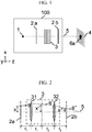
- FIG. 1 is a diagram illustrating an example of a configuration of an optical pattern generation device 100 according to a first embodiment.
- the optical pattern generation device 100 includes a laser light source 1 that emits laser light, a diffractive optical element 2a that changes the phase of laser light emitted from the laser light source 1 depending on the position on a plane perpendicular to the propagating direction of the laser light and emits laser light with a phase distribution, a diffractive optical element 2b that changes the phase of the laser light incident thereon depending on the position on a plane perpendicular to the propagating direction of the incident laser light and emits laser light forming an optical pattern, and a transfer optical system 3 that is provided between the diffractive optical elements 2a and 2b and transfers the phase distribution of the laser light emitted from the diffractive optical element 2a to that of the laser light incident on the diffractive optical element 2b.
- the optical pattern generation device 100 generates an optical pattern 6a by projecting the laser light emitted from the diffractive optical element 2b onto an image surface 4.
- a direction perpendicular to the optical axis 5 of the laser light emitted from the laser light source 1 and parallel to the figure is referred to as x-axis direction
- a direction perpendicular to the optical axis 5 of the laser light and perpendicular to the figure is referred to as y-axis direction
- a direction parallel to the optical axis 5 is referred to as z-axis direction.
- the optical pattern generation device 100 is used as a laser device for lighting, for example.
- the laser light source 1 is a light source that emits single-wavelength laser light.
- a semiconductor laser, a fiber laser, or a solid-state laser is used, for example.
- the diffractive optical elements 2a and 2b are elements each of which is made of glass or resin and has periodically patterned slits or irregularities on a substrate thereof, and convert light incident on the diffractive optical elements 2a and 2b so that diffracted light generated by the slits or irregularity patterns becomes light having a target intensity distribution on the image surface 4.
- the diffractive optical elements 2a and 2b each change the intensity and the phase of laser light incident on a corresponding one of the diffractive optical elements 2a and 2b by the slits or irregularity pattern of the corresponding one of the diffractive optical elements 2a and 2b depending on the position on a plane perpendicular to the propagating direction of the incident laser light, and each emit laser light having an intensity distribution and a phase distribution.
- the diffractive optical element 2a and the diffractive optical element 2b have respective surface irregularity patterns different from each other. As the surface patterns of the diffractive optical elements 2a and 2b are more continuous, that is, have more numbers of gradations, the diffraction efficiency is higher. In manufacturing, however, as the number of graduations is larger, processing becomes more difficult and the cost becomes higher.
- the transfer optical system 3 is an optical system includes a plurality of optical lenses.
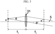
- FIG. 2 illustrates a configuration of the transfer optical system 3 including two lenses with focal distances of f 1 and f 2 .
- the configuration of the transfer optical system 3 will be described with reference to FIG. 2 .
- the focal distance of a lens 31 is represented by f 1
- the focal distance of a lens 32 is represented by f 2 .
- the sides of the lenses 31 and 32 closer to the laser light source 1 will be referred to as front sides, and the sides thereof farther from the laser light source 1 will be referred to as rear sides.
- the diffractive optical element 2a is positioned at the front-side focal position of the lens 31, and the diffractive optical element 2b is positioned at the rearside focal position of the lens 32.
- the distance between the lens 31 and the lens 32 is f 1 +f 2 , which is the sum of the respective focal distances.
- Transmitted light that is transmitted by the diffractive optical element 2a at a position at a distance x in the x-axis direction from the optical axis 5 is incident on the lens 31 at an incidence angle ⁇ .
- FIG. 3 For supplementary explanation, the manner in which light is refracted by the lens 31 is illustrated in FIG. 3 .
- the relations of the following formulas are therefore satisfied.
- the intensity distribution and the phase distribution at the distance x" on the diffractive optical element 2b are f 2 /f 1 times the intensity distribution and the phase distribution at the distance x on the diffractive optical element 2a
- the intensity distribution and the phase distribution at the angle ⁇ " on the diffractive optical element 2b are f 1 /f 2 times the intensity distribution and the phase distribution at the angle ⁇ on the diffractive optical element 2a.
- the intensity distribution and the phase distribution of light at the incidence surface of the diffractive optical element 2b are distributions obtained by transferring the intensity distribution and the phase distribution of light at the emission surface of the diffractive optical element 2a at the same magnification.
- the intensity distribution and the phase distribution can be regarded as distributions of intensity and phase, respectively, of light with respect to the position on a plane (a plane including the x axis and the y axis) perpendicular to the propagating direction of light at the diffractive optical element 2a.
- the intensity distribution and the phase distribution are distributions generated by conversion of the intensity and the phase of laser light by the diffractive optical element 2a.
- the diffractive optical element 2a may be configured to convert only either one of the intensity and the phase of laser light.
- the lens 31 and the lens 32 transfer the phase distribution of light at the incidence surface of the diffractive optical element 2b to the phase distribution of light at the emission surface of the diffractive optical element 2a.
- the configuration of the transfer optical system 3 illustrated in FIG. 2 is one example; the transfer optical system 3 is not limited thereto, and is only required to be any optical system that transfers the intensity distribution and the phase distribution of light at the emission surface of the diffractive optical element 2a to the intensity distribution and the phase distribution of light at the incidence surface of the diffractive optical element 2b.
- the diffractive optical element 2a and the diffractive optical element 2b are arranged at positions at which the intensity distribution and the phase distribution are transferred on the front side and the rear side of the transfer optical system 3.
- the diffractive optical element 2a converts the phase of light depending on the position on a plane (a plane including the x axis and the y axis) perpendicular to the propagating direction of light incident on the diffractive optical element 2a (hereinafter referred to as phase modulation).
- phase modulation Light emitted from the diffractive optical element 2a is transmitted through the transfer optical system 3 and incident on the diffractive optical element 2b.
- the intensity distribution and the phase distribution of light incident on the diffractive optical element 2b are distributions obtained by transferring the intensity distribution and the phase distribution of light at the emission surface of the diffractive optical element 2a by the transfer optical system 3.
- the diffractive optical element 2b modulates the phase of the light incident on the diffractive optical element 2b.
- Light emitted from the diffractive optical element 2b propagates and forms an image on the image surface 4.
- the light emitted from the laser light source 1 is subjected to phase modulation by the diffractive optical element 2a and the diffractive optical element 2b, propagates, and has, on the image surface 4, an intensity distribution 6a which corresponds to the phase distribution of light at the emission surface of the diffractive optical element 2b.
- the configuration is not limited thereto and may be a configuration including a plurality of diffractive optical elements and a plurality of transfer optical systems as long as the phase distribution of light at the emission surface of each of the diffractive optical elements is transferred onto the incidence surface of another diffractive optical element on which the light is next incident.
- a similar configuration is also applicable to a case where the intensity of laser light is converted and the laser light has an intensity distribution.
- the configuration in which one transfer optical system 3 is disposed between two diffractive optical elements 2a and 2b enables the phase distribution of light at the emission surface of the diffractive optical element 2a to be transferred to the phase distribution of light at the incidence surface of the diffractive optical element 2a.
- the irregularity pattern on the surface of the second diffractive optical element needs to be designed depending on the distribution of light incident on the second diffractive optical element in view of a change in a wavefront after propagation of light emitted from the first diffractive optical element.
- the second diffractive optical element 2b can be designed without consideration of a change in a wavefront due to propagation from the first diffractive optical element 2a. This produces advantages of simpler design and manufacture of diffractive optical elements than in the related art.
- phase distribution modulated by the diffractive optical element 2a is a distribution illustrated in FIG. 4A and the phase distribution modulated by the diffractive optical element 2b is a distribution illustrated in FIG. 4B
- light incident on the diffractive optical element 2a is subjected to phase modulation in the two-gradation distribution illustrated in FIG. 4A by the diffractive optical element 2a.
- Light emitted from the diffractive optical element 2a is transmitted through the transfer optical system 3 and incident on the diffractive optical element 2b.
- the phase distribution at the incidence surface of the diffractive optical element 2b is further subjected to phase modulation in the two-gradation distribution illustrated in FIG. 4B by the diffractive optical element 2b.
- the light emitted from the laser light source 1 is thus subjected to phase modulation by the diffractive optical element 2a and the diffractive optical element 2b.
- the phase distribution of light at the emission surface of the diffractive optical element 2b is a three-gradation phase distribution that is the sum of the two-gradation distribution of the diffractive optical element 2a and the two-gradation distribution of the diffractive optical element 2b.
- the number of gradations of the phase of the laser light emitted from the diffractive optical element 2b is larger than that of a phase change of laser light applied by each of the diffractive optical elements 2a and 2b.
- the configuration including two diffractive optical elements 2a and 2b of two gradations and one transfer optical system 3 is capable of generating a three-gradation phase distribution of light and increasing the number of gradations, by using the diffractive optical elements 2a and 2b of two gradations that are easily manufactured at low cost. This results in an advantageous effect of generating highly accurate optical patterns.
- n diffractive optical elements n is an integer equal to or more than 2 of two gradations and (n-1) transfer optical systems each being arranged between corresponding two of the diffractive optical elements, enables generation of an (n+1)-gradation phase distribution.
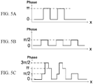
- the phase distribution modulated by the diffractive optical element 2a is a distribution illustrated in FIG. 5A and the phase distribution modulated by the diffractive optical element 2b is a distribution illustrated in FIG. 5B will be explained.
- the diffractive optical elements 2a and 2b have the same surface patterns as the phase distributions of the diffractive optical elements 2a and 2b illustrated in FIGS. 5A and 5B , respectively.
- the distribution of projections of the first diffractive optical element 2a and that of the second diffractive optical element 2b are shifted relative to each other within the plane perpendicular to the propagating direction of incident laser light.
- phase modulation in two gradations by the surface pattern of the diffractive optical element 2a illustrated in FIG. 5A .
- Light emitted from the diffractive optical element 2a is transmitted through the transfer optical system 3, and then incident on the diffractive optical element 2b.
- the phase distribution of light at the incidence surface of the diffractive optical element 2b is the phase distribution of light at the emission surface of the diffractive optical element 2a.
- Light incident on the diffractive optical element 2b is further subjected to phase modulation in two gradations by the surface pattern of the diffractive optical element 2b illustrated in FIG. 5B .
- the phase distribution of light at the emission surface of the diffractive optical element 2b is a four-gradation phase distribution that is the sum of the two-gradation distribution of the diffractive optical element 2a and the two-gradation distribution of the diffractive optical element 2b as illustrated in FIG. 5C .
- an irregularity pattern with a finer pitch than the pixel pitch of one diffractive optical element can be generated, and a phase distribution for a still larger number of pixels than the number of pixels of an optical pattern generated by using one diffractive optical element can be generated.
- the position of phase modulation by the irregularity pattern performed by the diffractive optical element 2a and the position of phase modulation by the irregularity pattern performed by the diffractive optical element 2b are different from each other, the phase of laser light emitted from the diffractive optical element 2a can be changed in still finer units in laser light emitted from the diffractive optical element 2b.
- any configuration including n diffractive optical elements (n is an integer equal to or more than 2) with distributions of irregularity patterns on their respective surfaces being shifted from each other and (n-1) transfer optical systems each being arranged between corresponding two of the diffractive optical elements, can generate a phase distribution for a larger number of pixels than that of an optical pattern generated by using one diffractive optical element. This results in an advantageous effect of generating highly accurate optical patterns.
- pixels of a surface irregularity pattern of the diffractive optical element needs to be finer and multivalued.
- the diffractive optical element needs to be subjected to a plurality of forming processes, which increases costs and reduces the accuracy.
- light can be subjected to phase modulation in a larger number of gradations than the number of gradations of the diffractive optical elements 2a and 2b, and more accurate optical patterns can be generated at lower costs than in the related art.
- the two diffractive optical elements 2a and 2b and the transfer optical system 3 between the two diffractive optical elements 2a and 2b are provided, which enables generation of an optical pattern on the image surface 4, the optical pattern corresponding to the phase distribution of light obtained by spatial phase modulation by the two diffractive optical elements 2a and 2b.
- use of the two diffractive optical elements 2a and 2b and the transfer optical system 3 enables the phase distribution of light at the emission surface of the diffractive optical element 2a to be further subjected to phase modulation by the diffractive optical element 2b.
- the phase distribution of light in two gradations obtained by modulation by the diffractive optical element 2a can further be modulated in two gradations by the diffractive optical element 2b.
- the phase distribution of laser light emitted from the laser light source 1 at the emission surface of the diffractive optical element 2b can be a phase distribution in three or more gradations.
- the configuration is not limited thereto and may be a configuration including a plurality of diffractive optical elements and a plurality of transfer optical systems as long as the phase distribution of light at the emission surface of each of the diffractive optical elements is transferred onto the incidence surface of another diffractive optical element on which the light is next incident.
- the number of gradations is not limited. When the number of diffractive optical elements is more than one, similar effects are produced on increase in values and pixels.
- the optical pattern generation device 100 includes: the first laser light source 1 for emitting first laser light; the first diffractive optical element 2a for changing the phase of the first laser light depending on the position on a plane perpendicular to the propagating direction of the first laser light and emitting laser light having a phase distribution; the second diffractive optical element 2b for changing the phase of incident laser light depending on the position on a plane perpendicular to the propagating direction of the incident laser light and emitting laser light for forming an optical pattern; and the transfer optical system 3 disposed between the first and second diffractive optical elements 2a and 2b, for transferring the phase distribution of laser light emitted from the first diffractive optical element to the phase distribution of laser light incident on the second diffractive optical element 2b.
- This configuration enables the second diffractive optical element 2b to be simply designed without consideration of a change in a wavefront due to propagation of light emitted from the first diffractive optical element 2a.
- the first diffractive optical element 2a changes the intensity of the first laser light depending on the position on the plane perpendicular to the propagating direction of the first laser light
- the transfer optical system 3 transfers the intensity distribution of the laser light whose intensity is changed by the first diffractive optical element 2a to the intensity distribution of laser light incident on the second diffractive optical element 2b.
- the number of gradations of the phase of the laser light emitted from the second diffractive optical element 2b is larger than that of a phase change of laser light applied by each of the first and second diffractive optical elements 2a and 2b.
- This configuration enables phase modulation of laser light with a larger number of gradations than that of each of the diffractive optical elements 2a and 2b by using the diffractive optical elements 2a and 2b with a small number of gradations.
- the position where the phase is changed by the change in phase performed by the first diffractive optical element 2a and the position where the phase is changed by the change in phase performed by the second diffractive optical element 2b are different. This configuration enables phase distribution to be generated with a larger number of pixels than that of an optical pattern generated by using one diffractive optical element.
- This configuration enables the individual diffractive optical elements to be designed without consideration of a change in a wavefront due to propagation of light emitted from the diffractive optical elements. Furthermore, use of a large number of diffractive optical elements enables phase modulation with a large number of gradations on laser light that forms an optical pattern.
- two diffractive optical elements 2a and 2b are arranged on the optical axis 5 in the first embodiment
- two diffractive optical elements 2a and 2b can be arranged on and displaced from the optical axis and a case where either one of the diffractive optical elements 2a and 2b is not arranged on the optical axis 5 is included.
- FIGS. 6 and 7 are diagrams illustrating examples of a configuration of an optical pattern generation device 100 according to the second embodiment.
- the diffractive optical element 2a is positioned between the laser light source 1 and the transfer optical system 3, and moves in a direction perpendicular to the optical axis 5.
- the diffractive optical element 2b is positioned between the transfer optical system 3 and the diffractive optical element 2b, and moves in a direction perpendicular to the optical axis 5.
- the movement displaces either one of the first and second diffractive optical elements 2a and 2b from the optical path through which laser light emitted from the laser light source 1 passes before forming an optical pattern.
- the optical pattern generation device 100 has a configuration in which either one of the diffractive optical elements 2a and 2b can be moved to be displaced from the optical path through which laser light emitted from the laser light source 1 passes before forming an optical pattern.
- FIG. 6 is different from the configuration in FIG. 1 in that the diffractive optical element 2b is not on the optical axis 5.
- Light emitted from the laser light source 1 is incident on the diffractive optical element 2a.
- Light incident on the diffractive optical element 2a is subjected to phase modulation by the diffractive optical element 2a.
- the phase distribution and the intensity distribution of light at the emission surface of the diffractive optical element 2a are transferred by the transfer optical system 3 to the position corresponding to the position where the diffractive optical element 2b is arranged in FIG. 1 .
- the transferred light propagates, and has, on the image surface 4, an intensity distribution 6b which corresponds to the phase distribution of light at the emission surface of the diffractive optical element 2a.
- FIG. 7 is different from the configuration in FIG. 1 in that the diffractive optical element 2a is not on the optical axis 5.
- Light emitted from the laser light source 1 is incident on the transfer optical system 3.
- the transfer optical system 3 transfers the intensity distribution and the phase distribution of light at the position corresponding to the position where the diffractive optical element 2a is arranged in FIG. 1 to the incidence surface of the diffractive optical element 2b.
- the light incident on the diffractive optical element 2b is subjected to phase modulation by the diffractive optical element 2b.
- Light emitted from the diffractive optical element 2b propagates, and has, on the image surface 4, an intensity distribution 6c which corresponds to the phase distribution of light at the emission surface of the diffractive optical element 2b.
- the phase distributions obtained by the diffractive optical elements 2a and 2b need to be changed depending on the positions where the diffractive optical elements 2a and 2b are arranged in the related art in which the transfer optical system 3 is not included.
- the transfer optical system 3 is used, which enables an optical pattern to be generated on the image surface 4 even in a case where the distances from the emission surfaces of the diffractive optical elements to the image surface 4 are different such as a case where light emitted from the laser light source 1 is transmitted through two diffractive optical elements 2a and 2b, a case where the light is transmitted only through the diffractive optical element 2a, and a case where the light is transmitted only through the diffractive optical element 2b.
- images of three patterns can be generated by the two diffractive optical elements 2a and 2b.
- the configuration including two diffractive optical elements 2a and 2b that can be inserted on and removed from the optical axis 5, and the transfer optical system 3 between the diffractive optical elements 2a and 2b is used, which enables irradiation in different patterns on the image surface 4 in the cases where light emitted from the laser light source 1 is transmitted only through the diffractive optical element 2a, the light is transmitted only through the diffractive optical element 2b, and the light is transmitted through both the diffractive optical element 2a and the diffractive optical element 2b.
- An effect of enabling generation of images of three optical patterns by two diffractive optical elements 2a and 2b is thus produced.
- the configuration is not limited thereto and may be a configuration including n diffractive optical elements (n is an integer equal to or more than 2) of two gradations and (n-1) transfer optical systems each being arranged between corresponding two of the diffractive optical elements as long as the phase distribution at the emission surface of each of the diffractive optical elements is transferred onto the incidence surface of another diffractive optical element.
- n diffractive optical elements n is an integer equal to or more than 2 of two gradations and (n-1) transfer optical systems each being arranged between corresponding two of the diffractive optical elements as long as the phase distribution at the emission surface of each of the diffractive optical elements is transferred onto the incidence surface of another diffractive optical element.
- the optical pattern generation device 100 is capable of generating more kinds of patterns than the number of diffractive optical elements, which enables more accurate optical patterns to be generated at lower costs than those in the related art.
- the optical pattern generation device 100 is characterized in that either one of the first and second diffractive optical elements 2a and 2b can be moved to be displaced from the optical path through which the first laser light passes before forming an optical pattern.
- This configuration produces an effect of enabling generation of images of three optical patterns by two diffractive optical elements 2a and 2b.
- FIGS. 8 to 10 are diagrams illustrating examples of a configuration of an optical pattern generation device 100 according to the third embodiment.
- the third embodiment is different from the second embodiment in that two laser light sources 1a and 1b are used and that a mirror 7 is provided between the transfer optical system 3 and the diffractive optical element 2b.
- the laser light source 1b is a light source that emits single-wavelength laser light.
- a semiconductor laser, a fiber laser, or a solid-state laser is used, for example.
- the wavelength of light emitted by the laser light source 1b may be the same as or different from that of light emitted by the laser light source 1a.
- the mirror 7 is an optical component that transmits some incident light and reflects some incident light.
- An example of the mirror 7 is a beam splitter.
- the laser light source 1b is arranged at a certain position so that light emitted by the laser light source 1b is incident on the emission surface of the mirror 7 from which light emitted from the laser light source 1a is emitted.
- the mirror 7 is disposed between the transfer optical system 3 and the diffractive optical element 2b.
- Light emitted from the laser light source 1b is incident on the mirror 7.
- the light emitted from the laser light source 1b and incident on the mirror 7 is reflected by the surface of the mirror 7 and incident on the diffractive optical element 2b.
- the light incident on the diffractive optical element 2b is subjected to phase modulation, and emitted as a pattern onto the image surface 4.
- Light emitted from the laser light source 1a is incident on the diffractive optical element 2a.
- the light incident on the diffractive optical element 2a is subjected to phase modulation and emitted by the diffractive optical element 2a.
- the light emitted from the diffractive optical element 2a is transmitted through the transfer optical system 3 and the mirror 7, and incident on the diffractive optical element 2b.
- the light incident on the diffractive optical element 2b is subjected to phase modulation, and emitted as a pattern onto the image surface 4.
- the color of the pattern on the image surface 4 is a color obtained by additive mixing of the color of the laser light source 1a and the color of the laser light source 1b.
- adjustment of an output value from the laser light source 1a and an output value from the laser light source 1b enables generation of at least one pattern with multiple colors.
- use of the laser light source 1a and the laser light source 1b and provision of the mirror 7 between the transfer optical system 3 and the diffractive optical element 2b enable generation of at least one pattern with multiple colors.
- use of the laser light source 1a and the laser light source 1b and provision of the mirror 7 between the transfer optical system 3 and the diffractive optical element 2b enable four kinds of patterns to be generated by two diffractive optical elements 2a and 2b and two laser light sources.
- the optical pattern generation device 100 of the third embodiment having the configuration as described above in which the laser light source 1a and the laser light source 1b are used and the mirror 7 is provided between the transfer optical system 3 and the diffractive optical element 2b also produces effects similar to those in the first and second embodiments. Additionally, the optical pattern generation device 100 of the third embodiment in which the laser light source 1a and the laser light source 1b are used and the mirror 7 is provided between the transfer optical system 3 and the diffractive optical element 2b produces an effect of enabling generation of at least one pattern with multiple colors. Furthermore, four kinds of patterns can be generated by two diffractive optical elements 2a and 2b and two laser light sources 1a and 1b. Furthermore, display of the four kinds of patterns while continuously switching between the patterns produces an effect of enabling the patterns to be animated.
- the configuration is not limited thereto and may be a configuration including a plurality of laser light sources, a plurality of diffractive optical elements, a plurality of transfer optical systems, and a plurality of mirrors as long as the phase distribution at the emission surface of each of the diffractive optical elements is transferred onto the incidence surface of another diffractive optical element.
- the optical pattern generation device 100 includes: the second laser light source 1b for emitting second laser light; and the mirror 7 for transmitting laser light which is to be incident on the second diffractive optical element and onto which the phase distribution is transferred by the transfer optical system 3, and reflecting the second laser light, in which the second diffractive optical element 2b changes the phase of laser light reflected by the mirror 7 depending on the position on a plane perpendicular to the propagating direction of laser light reflected by the mirror 7, and emits laser light that form an optical pattern different from that formed by the first laser light.
- This configuration enables generation of at least one optical pattern with multiple colors in a case where the color of light emitted from the laser light source 1a and the color of light emitted from the laser light source 1b are different from each other.
- the second laser light has a wavelength different from that of the first laser light. This configuration enables the color of light emitted from the laser light source 1a and the color of light emitted from the laser light source 1b to be different from each other.
- either one of the first and second diffractive optical elements 2a and 2b can be moved to be displaced from the optical path through which the first laser light passes before forming an optical pattern.
- This configuration produces an effect of enabling the four kinds of patterns to be animated by displaying the patterns while continuously switching between the patterns.
- 1, 1a, 1b laser light source, 2a, 2b: diffractive optical element, 3: transfer optical system, 4: image surface, 5: optical axis, 6a, 6b, 6c, 6d, 6e, 6f: optical pattern, 7: mirror, 31, 32: lens, 100: optical pattern generation device.
Landscapes
- Physics & Mathematics (AREA)
- General Physics & Mathematics (AREA)
- Optics & Photonics (AREA)
- Diffracting Gratings Or Hologram Optical Elements (AREA)
- Laser Beam Processing (AREA)
- Exposure And Positioning Against Photoresist Photosensitive Materials (AREA)
Abstract
Description
- The present invention relates to an optical pattern generation device that generates optical patterns.
- Diffractive optical elements (DOEs) that each convert incident light into a desired pattern have been used in various optical devices and the like. Typical applications include material processing, printing, optical measurement, illumination, etc. For example, in a laser beam machine, a diffractive optical element has a function of making an incident beam branch into a plurality of beams. In addition, with positions and intensities of branching beams being designed, diffractive optical elements are also used in lighting systems that generate desired patterns.
- A diffractive optical element is an element having periodically patterned slits or irregularities on a substrate, and uses diffracted light generated by the influence of the slits or irregularity pattern to convert incident light into light with a target intensity distribution or phase distribution. In particular, a phase-type diffractive optical element converts the phase distribution of incident light into a phase distribution that forms a desired pattern on an image surface, which results in much higher energy efficiency of converted light with respect to incident light than that of an amplitude-type diffractive optical element. Phase-type diffractive optical elements are therefore used not only as diffractive optical elements with simple patterns for providing uniform intensity distributions but also as diffractive optical elements generating diffraction patterns of complicated patterns.
- Examples of optical pattern generation devices in which diffractive optical elements of the related art are used include one device including one diffractive optical element and generating one pattern. In addition, the examples include one device which includes two diffractive optical elements, and in which light from a light source is transmitted through the two diffractive optical elements, thereby generating a pattern so as to diffract the light at an angle larger than that of diffraction by one diffractive optical element (
Patent Literature 1, for example). The surface irregularity patterns of such diffractive optical elements are each designed so that a desired pattern is formed on an image surface by using a specific wavelength. - Patent Literature 1:
JP 2014-209237 A - In an optical pattern generation device of the related art including two diffractive optical elements, it is necessary to obtain the distribution of light incident on the second diffractive optical element in view of a change in a wavefront due to propagation of light emitted from the first diffractive optical element, and design the surface irregularity pattern of the second diffractive optical element depending on the distribution of light incident on the second diffractive optical element. This causes problems in that the design and the manufacture of the surface pattern of the second diffractive optical element are complicated.
- The present invention has been made to solve such problems as described above, and an object thereof is to provide an optical pattern generation device enabling a second diffractive optical element to be simply designed without consideration of a change in a wavefront due to propagation of light emitted from a first diffractive optical element.
- An optical pattern generation device according to the present invention includes: a first laser light source for emitting first laser light; a first diffractive optical element for changing a phase of the first laser light depending on a position on a plane perpendicular to a propagating direction of the first laser light, and emitting laser light having a phase distribution; a second diffractive optical element for changing a phase of incident laser light depending on a position on a plane perpendicular to a propagating direction of the incident laser light, and emitting laser light for forming an optical pattern; and a transfer optical system disposed between the first and second diffractive optical elements, for transferring the phase distribution of the laser light emitted from the first diffractive optical element to a phase distribution of laser light incident on the second diffractive optical element.
- According to the present invention, a second diffractive optical element can be simply designed without consideration of a change in a wavefront due to propagation of light emitted from a first diffractive optical element.
-
-
FIG. 1 illustrates an example of a configuration of an opticalpattern generation device 100 according to a first embodiment. -
FIG. 2 illustrates an example of a configuration of a transferoptical system 3 according to the first embodiment. -
FIG. 3 is a diagram illustrating refraction of light by alens 31 according to the first embodiment. -
FIG. 4 illustrates an example of phase distributions of phase modulation performed by diffractiveoptical elements -
FIG. 5 illustrates an example of phase distributions of phase modulation performed by the diffractiveoptical elements -
FIG. 6 illustrates an example of a configuration of an opticalpattern generation device 100 according to a second embodiment. -
FIG. 7 illustrates an example of a configuration of the opticalpattern generation device 100 according to the second embodiment. -
FIG. 8 illustrates an example of a configuration of an opticalpattern generation device 100 according to a third embodiment. -
FIG. 9 illustrates an example of a configuration of the opticalpattern generation device 100 according to the third embodiment. -
FIG. 10 illustrates an example of a configuration of the opticalpattern generation device 100 according to the third embodiment. -
FIG. 11 illustrates an example of a configuration of the opticalpattern generation device 100 according to the third embodiment. - Embodiments of the present invention will now be described.
-
FIG. 1 is a diagram illustrating an example of a configuration of an opticalpattern generation device 100 according to a first embodiment. The opticalpattern generation device 100 includes alaser light source 1 that emits laser light, a diffractiveoptical element 2a that changes the phase of laser light emitted from thelaser light source 1 depending on the position on a plane perpendicular to the propagating direction of the laser light and emits laser light with a phase distribution, a diffractiveoptical element 2b that changes the phase of the laser light incident thereon depending on the position on a plane perpendicular to the propagating direction of the incident laser light and emits laser light forming an optical pattern, and a transferoptical system 3 that is provided between the diffractiveoptical elements optical element 2a to that of the laser light incident on the diffractiveoptical element 2b. The opticalpattern generation device 100 generates anoptical pattern 6a by projecting the laser light emitted from the diffractiveoptical element 2b onto animage surface 4. InFIG. 1 , a direction perpendicular to theoptical axis 5 of the laser light emitted from thelaser light source 1 and parallel to the figure is referred to as x-axis direction, a direction perpendicular to theoptical axis 5 of the laser light and perpendicular to the figure is referred to as y-axis direction, and a direction parallel to theoptical axis 5 is referred to as z-axis direction. Note that in each of subsequent figures, the same reference numerals represent the same or corresponding components. The opticalpattern generation device 100 is used as a laser device for lighting, for example. - The
laser light source 1 is a light source that emits single-wavelength laser light. For thelaser light source 1, a semiconductor laser, a fiber laser, or a solid-state laser is used, for example. - The diffractive
optical elements optical elements image surface 4. Specifically, the diffractiveoptical elements optical elements optical elements optical element 2a and the diffractiveoptical element 2b have respective surface irregularity patterns different from each other. As the surface patterns of the diffractiveoptical elements - The transfer
optical system 3 is an optical system includes a plurality of optical lenses.FIG. 2 illustrates a configuration of the transferoptical system 3 including two lenses with focal distances of f1 and f2. The configuration of the transferoptical system 3 will be described with reference toFIG. 2 . The focal distance of alens 31 is represented by f1, and the focal distance of alens 32 is represented by f2. In addition, the sides of thelenses laser light source 1 will be referred to as front sides, and the sides thereof farther from thelaser light source 1 will be referred to as rear sides. The diffractiveoptical element 2a is positioned at the front-side focal position of thelens 31, and the diffractiveoptical element 2b is positioned at the rearside focal position of thelens 32. In this case, the distance between thelens 31 and thelens 32 is f1+f2, which is the sum of the respective focal distances. - Transmitted light that is transmitted by the diffractive
optical element 2a at a position at a distance x in the x-axis direction from theoptical axis 5 is incident on thelens 31 at an incidence angle θ. The light incident on thelens 31 at the incidence angle θ is refracted by thelens 31 at an angle of θ'=x/f1 with respect to theoptical axis 5. In addition, the light refracted by thelens 31 passes a position at a distance of x'=θf1 from theoptical axis 5 at the focal position on the emitting side of thelens 31. Thus, thelens 31 converts light emitted at the distance x from theoptical axis 5 on the diffractiveoptical element 2a and at the angle θ with respect to theoptical axis 5, into light at the distance x'=θf1 from theoptical axis 5 at the focal distance on the emitting side of thelens 31 and with the angle θ'=x/f1 with respect to theoptical axis 5. - For supplementary explanation, the manner in which light is refracted by the
lens 31 is illustrated inFIG. 3 . A line connecting the position at the distance x from theoptical axis 5 and the center 35 of thelens 31 has an angle of θ' with respect to theoptical axis 5. The relations of the following formulas are therefore satisfied.

- Thus, the following formula is satisfied.

- In addition, the relations of the following formulas are satisfied.


- Thus, the following formula is satisfied.

- In the description above, the relations of the formulas (1) and (2) are used.
- In a similar manner, in
FIG. 2 , thelens 32 converts light at the distance x' from the optical axis at the front-side focal position, into light with an angle of θ"=x'/f2 with respect to theoptical axis 5 on the diffractiveoptical element 2b, and converts light emitted at the angle θ' with respect to theoptical axis 5, into light at the distance x"=θ'f2 from theoptical axis 5. In other words, by thelens 31 and thelens 32, light at the distance x from theoptical axis 5 on the diffractiveoptical element 2a and emitted at the angle θ with respect to theoptical axis 5 is converted into light at the distance x"=θ'f2=x(f2/f1) from theoptical axis 5 on the diffractiveoptical element 2b and with the angle θ"=x'/f2=θ(f1/f2) with respect to theoptical axis 5. Thus, the intensity distribution and the phase distribution at the distance x" on the diffractiveoptical element 2b are f2/f1 times the intensity distribution and the phase distribution at the distance x on the diffractiveoptical element 2a, and the intensity distribution and the phase distribution at the angle θ" on the diffractiveoptical element 2b are f1/f2 times the intensity distribution and the phase distribution at the angle θ on the diffractiveoptical element 2a. In particular, in a case where the focal distances of thelens 31 and thelens 32 are equal to each other, the intensity distribution and the phase distribution of light at the incidence surface of the diffractiveoptical element 2b are distributions obtained by transferring the intensity distribution and the phase distribution of light at the emission surface of the diffractiveoptical element 2a at the same magnification. - While conversion of light with respect to distance in the x-axis direction has been explained herein, the same explanation is also applicable to that in the y-axis direction. Thus, the intensity distribution and the phase distribution can be regarded as distributions of intensity and phase, respectively, of light with respect to the position on a plane (a plane including the x axis and the y axis) perpendicular to the propagating direction of light at the diffractive
optical element 2a. The intensity distribution and the phase distribution are distributions generated by conversion of the intensity and the phase of laser light by the diffractiveoptical element 2a. Note that the diffractiveoptical element 2a may be configured to convert only either one of the intensity and the phase of laser light. In this case, thelens 31 and thelens 32 transfer the phase distribution of light at the incidence surface of the diffractiveoptical element 2b to the phase distribution of light at the emission surface of the diffractiveoptical element 2a. - The configuration of the transfer
optical system 3 illustrated inFIG. 2 is one example; the transferoptical system 3 is not limited thereto, and is only required to be any optical system that transfers the intensity distribution and the phase distribution of light at the emission surface of the diffractiveoptical element 2a to the intensity distribution and the phase distribution of light at the incidence surface of the diffractiveoptical element 2b. The diffractiveoptical element 2a and the diffractiveoptical element 2b are arranged at positions at which the intensity distribution and the phase distribution are transferred on the front side and the rear side of the transferoptical system 3. - Next, operation of generating an optical pattern performed by the optical
pattern generation device 100 according to the first embodiment will be explained. - Light emitted from the
laser light source 1 is incident on the diffractiveoptical element 2a. - The diffractive
optical element 2a converts the phase of light depending on the position on a plane (a plane including the x axis and the y axis) perpendicular to the propagating direction of light incident on the diffractiveoptical element 2a (hereinafter referred to as phase modulation). Light emitted from the diffractiveoptical element 2a is transmitted through the transferoptical system 3 and incident on the diffractiveoptical element 2b. In this process, the intensity distribution and the phase distribution of light incident on the diffractiveoptical element 2b are distributions obtained by transferring the intensity distribution and the phase distribution of light at the emission surface of the diffractiveoptical element 2a by the transferoptical system 3. The diffractiveoptical element 2b modulates the phase of the light incident on the diffractiveoptical element 2b. Light emitted from the diffractiveoptical element 2b propagates and forms an image on theimage surface 4. Thus, the light emitted from thelaser light source 1 is subjected to phase modulation by the diffractiveoptical element 2a and the diffractiveoptical element 2b, propagates, and has, on theimage surface 4, anintensity distribution 6a which corresponds to the phase distribution of light at the emission surface of the diffractiveoptical element 2b. - While the configuration including two diffractive
optical elements optical system 3 has been described above, the configuration is not limited thereto and may be a configuration including a plurality of diffractive optical elements and a plurality of transfer optical systems as long as the phase distribution of light at the emission surface of each of the diffractive optical elements is transferred onto the incidence surface of another diffractive optical element on which the light is next incident. In addition, while a case where laser light is subjected to phase modulation by the diffractiveoptical elements - In the present embodiment, use of the configuration in which one transfer
optical system 3 is disposed between two diffractiveoptical elements optical element 2a to be transferred to the phase distribution of light at the incidence surface of the diffractiveoptical element 2a. In the optical pattern generation device of the related art, the irregularity pattern on the surface of the second diffractive optical element needs to be designed depending on the distribution of light incident on the second diffractive optical element in view of a change in a wavefront after propagation of light emitted from the first diffractive optical element. In contrast, in the opticalpattern generation device 100 according to the present embodiment, the second diffractiveoptical element 2b can be designed without consideration of a change in a wavefront due to propagation from the first diffractiveoptical element 2a. This produces advantages of simpler design and manufacture of diffractive optical elements than in the related art. - Next, another advantageous effect of the first embodiment obtained by using the diffractive
optical elements optical system 3 will be explained with reference toFIG. 4 , the effect of enabling phase modulation of light with more number of gradations than that of one diffractive optical element even though the diffractiveoptical elements - For example, in a case where the phase distribution modulated by the diffractive
optical element 2a is a distribution illustrated inFIG. 4A and the phase distribution modulated by the diffractiveoptical element 2b is a distribution illustrated inFIG. 4B , light incident on the diffractiveoptical element 2a is subjected to phase modulation in the two-gradation distribution illustrated inFIG. 4A by the diffractiveoptical element 2a. Light emitted from the diffractiveoptical element 2a is transmitted through the transferoptical system 3 and incident on the diffractiveoptical element 2b. The phase distribution at the incidence surface of the diffractiveoptical element 2b is further subjected to phase modulation in the two-gradation distribution illustrated inFIG. 4B by the diffractiveoptical element 2b. The light emitted from thelaser light source 1 is thus subjected to phase modulation by the diffractiveoptical element 2a and the diffractiveoptical element 2b. As illustrated inFIG. 4C , the phase distribution of light at the emission surface of the diffractiveoptical element 2b is a three-gradation phase distribution that is the sum of the two-gradation distribution of the diffractiveoptical element 2a and the two-gradation distribution of the diffractiveoptical element 2b. Thus, the number of gradations of the phase of the laser light emitted from the diffractiveoptical element 2b is larger than that of a phase change of laser light applied by each of the diffractiveoptical elements - As described above, the configuration including two diffractive
optical elements optical system 3 is capable of generating a three-gradation phase distribution of light and increasing the number of gradations, by using the diffractiveoptical elements - While the configuration including two diffractive
optical elements optical system 3 is explained inFIG. 4 , use of a configuration including n diffractive optical elements (n is an integer equal to or more than 2) of two gradations and (n-1) transfer optical systems each being arranged between corresponding two of the diffractive optical elements, enables generation of an (n+1)-gradation phase distribution. - Next, another advantageous effect of the first embodiment obtained by using the diffractive
optical elements optical system 3 will be explained with reference toFIG. 5 , the effect of enabling generation of a phase distribution for a larger number of pixels than that of an optical pattern generated by using one diffractive optical element. Note that pixels are used as the smallest units constituting an image formed by the generated optical pattern. - For example, a case where the phase distribution modulated by the diffractive
optical element 2a is a distribution illustrated inFIG. 5A and the phase distribution modulated by the diffractiveoptical element 2b is a distribution illustrated inFIG. 5B will be explained. Note that the diffractiveoptical elements optical elements FIGS. 5A and 5B , respectively. Specifically, inFIGS. 5A and 5B , the distribution of projections of the first diffractiveoptical element 2a and that of the second diffractiveoptical element 2b are shifted relative to each other within the plane perpendicular to the propagating direction of incident laser light. - In this case, light incident on the diffractive
optical element 2a is subjected to phase modulation in two gradations by the surface pattern of the diffractiveoptical element 2a illustrated inFIG. 5A . Light emitted from the diffractiveoptical element 2a is transmitted through the transferoptical system 3, and then incident on the diffractiveoptical element 2b. The phase distribution of light at the incidence surface of the diffractiveoptical element 2b is the phase distribution of light at the emission surface of the diffractiveoptical element 2a. Light incident on the diffractiveoptical element 2b is further subjected to phase modulation in two gradations by the surface pattern of the diffractiveoptical element 2b illustrated inFIG. 5B . Because light emitted from thelaser light source 1 is subjected to phase modulation by the diffractiveoptical element 2a and the diffractiveoptical element 2b, the phase distribution of light at the emission surface of the diffractiveoptical element 2b is a four-gradation phase distribution that is the sum of the two-gradation distribution of the diffractiveoptical element 2a and the two-gradation distribution of the diffractiveoptical element 2b as illustrated inFIG. 5C . Because the projection patterns of the diffractiveoptical elements optical element 2a and the position of phase modulation by the irregularity pattern performed by the diffractiveoptical element 2b are different from each other, the phase of laser light emitted from the diffractiveoptical element 2a can be changed in still finer units in laser light emitted from the diffractiveoptical element 2b. - While the configuration including two diffractive
optical elements optical system 3 is explained inFIG. 5 , any configuration including n diffractive optical elements (n is an integer equal to or more than 2) with distributions of irregularity patterns on their respective surfaces being shifted from each other and (n-1) transfer optical systems each being arranged between corresponding two of the diffractive optical elements, can generate a phase distribution for a larger number of pixels than that of an optical pattern generated by using one diffractive optical element. This results in an advantageous effect of generating highly accurate optical patterns. - In general, for making an image generated by a diffractive optical element more accurate, pixels of a surface irregularity pattern of the diffractive optical element needs to be finer and multivalued. In the related art, for achieving multiple values by one diffractive optical element, the diffractive optical element needs to be subjected to a plurality of forming processes, which increases costs and reduces the accuracy. In contrast, in the present embodiment, light can be subjected to phase modulation in a larger number of gradations than the number of gradations of the diffractive
optical elements - As described above, according to the first embodiment, the two diffractive
optical elements optical system 3 between the two diffractiveoptical elements image surface 4, the optical pattern corresponding to the phase distribution of light obtained by spatial phase modulation by the two diffractiveoptical elements optical elements optical system 3 enables the phase distribution of light at the emission surface of the diffractiveoptical element 2a to be further subjected to phase modulation by the diffractiveoptical element 2b. For example, in a case where the diffractiveoptical element 2a and the diffractiveoptical element 2b have surface patterns in two gradations, the phase distribution of light in two gradations obtained by modulation by the diffractiveoptical element 2a can further be modulated in two gradations by the diffractiveoptical element 2b. As a result, the phase distribution of laser light emitted from thelaser light source 1 at the emission surface of the diffractiveoptical element 2b can be a phase distribution in three or more gradations. - While the configuration including two diffractive
optical elements optical system 3 has been described above, the configuration is not limited thereto and may be a configuration including a plurality of diffractive optical elements and a plurality of transfer optical systems as long as the phase distribution of light at the emission surface of each of the diffractive optical elements is transferred onto the incidence surface of another diffractive optical element on which the light is next incident. - In addition, while the configuration including two diffractive
optical elements - As described above, the optical
pattern generation device 100 according to the present embodiment includes: the firstlaser light source 1 for emitting first laser light; the first diffractiveoptical element 2a for changing the phase of the first laser light depending on the position on a plane perpendicular to the propagating direction of the first laser light and emitting laser light having a phase distribution; the second diffractiveoptical element 2b for changing the phase of incident laser light depending on the position on a plane perpendicular to the propagating direction of the incident laser light and emitting laser light for forming an optical pattern; and the transferoptical system 3 disposed between the first and second diffractiveoptical elements optical element 2b. This configuration enables the second diffractiveoptical element 2b to be simply designed without consideration of a change in a wavefront due to propagation of light emitted from the first diffractiveoptical element 2a. - In addition, in the optical
pattern generation device 100 according to the present embodiment, the first diffractiveoptical element 2a changes the intensity of the first laser light depending on the position on the plane perpendicular to the propagating direction of the first laser light, and the transferoptical system 3 transfers the intensity distribution of the laser light whose intensity is changed by the first diffractiveoptical element 2a to the intensity distribution of laser light incident on the second diffractiveoptical element 2b. This configuration enables the second diffractiveoptical element 2b to be simply designed without consideration of a change in a wavefront due to propagation of light emitted from the first diffractiveoptical element 2a, even in a case where the laser light emitted from the first diffractiveoptical element 2a has an intensity distribution. - In addition, in the optical
pattern generation device 100 according to the present embodiment, the number of gradations of the phase of the laser light emitted from the second diffractiveoptical element 2b is larger than that of a phase change of laser light applied by each of the first and second diffractiveoptical elements optical elements optical elements - In addition, in the optical
pattern generation device 100 according to the present embodiment, in the laser light emitted from the second diffractiveoptical element 2b, the position where the phase is changed by the change in phase performed by the first diffractiveoptical element 2a and the position where the phase is changed by the change in phase performed by the second diffractiveoptical element 2b are different. This configuration enables phase distribution to be generated with a larger number of pixels than that of an optical pattern generated by using one diffractive optical element. - In addition, the optical
pattern generation device 100 according to the present embodiment includes: the firstlaser light source 1 for emitting laser light; the first to N-th diffractive optical elements (N is an integer equal to or more than 2) each for changing the phase of incident laser light depending on the position on the plane perpendicular to the propagating direction of the incident laser light and emitting laser light having a phase distribution; n transfer optical systems (n = 1, ..., N-1) each arranged between the n-th diffractive optical element and the (n+1)-th diffractive optical element, for transferring the phase distribution of laser light emitted from the n-th diffractive optical element to the phase distribution of laser light incident on the (n+1)-th diffractive optical element, in which the laser light emitted from the first laser light source is incident on the first diffractive optical element, and laser light whose phase is changed by the N-th diffractive optical element is laser light that forms an optical pattern. This configuration enables the individual diffractive optical elements to be designed without consideration of a change in a wavefront due to propagation of light emitted from the diffractive optical elements. Furthermore, use of a large number of diffractive optical elements enables phase modulation with a large number of gradations on laser light that forms an optical pattern. - While two diffractive
optical elements optical axis 5 in the first embodiment, in a second embodiment, two diffractiveoptical elements optical elements optical axis 5 is included. -
FIGS. 6 and 7 are diagrams illustrating examples of a configuration of an opticalpattern generation device 100 according to the second embodiment. The diffractiveoptical element 2a is positioned between thelaser light source 1 and the transferoptical system 3, and moves in a direction perpendicular to theoptical axis 5. The diffractiveoptical element 2b is positioned between the transferoptical system 3 and the diffractiveoptical element 2b, and moves in a direction perpendicular to theoptical axis 5. The movement displaces either one of the first and second diffractiveoptical elements laser light source 1 passes before forming an optical pattern. Thus, the opticalpattern generation device 100 according to the second embodiment has a configuration in which either one of the diffractiveoptical elements laser light source 1 passes before forming an optical pattern. - Operation of the optical
pattern generation device 100 according to the second embodiment will now be explained. -
FIG. 6 is different from the configuration inFIG. 1 in that the diffractiveoptical element 2b is not on theoptical axis 5. Light emitted from thelaser light source 1 is incident on the diffractiveoptical element 2a. Light incident on the diffractiveoptical element 2a is subjected to phase modulation by the diffractiveoptical element 2a. The phase distribution and the intensity distribution of light at the emission surface of the diffractiveoptical element 2a are transferred by the transferoptical system 3 to the position corresponding to the position where the diffractiveoptical element 2b is arranged inFIG. 1 . The transferred light propagates, and has, on theimage surface 4, anintensity distribution 6b which corresponds to the phase distribution of light at the emission surface of the diffractiveoptical element 2a. -
FIG. 7 is different from the configuration inFIG. 1 in that the diffractiveoptical element 2a is not on theoptical axis 5. Light emitted from thelaser light source 1 is incident on the transferoptical system 3. The transferoptical system 3 transfers the intensity distribution and the phase distribution of light at the position corresponding to the position where the diffractiveoptical element 2a is arranged inFIG. 1 to the incidence surface of the diffractiveoptical element 2b. The light incident on the diffractiveoptical element 2b is subjected to phase modulation by the diffractiveoptical element 2b. Light emitted from the diffractiveoptical element 2b propagates, and has, on theimage surface 4, anintensity distribution 6c which corresponds to the phase distribution of light at the emission surface of the diffractiveoptical element 2b. - Next, advantageous effects of the optical
pattern generation device 100 according to the second embodiment will be explained. - Because the distances from the emission surfaces of the diffractive optical elements to the
image surface 4 are different depending on the positions where the respective diffractiveoptical elements optical elements optical elements optical system 3 is not included. - In contrast, with the optical
pattern generation device 100 according to the second embodiment, the transferoptical system 3 is used, which enables an optical pattern to be generated on theimage surface 4 even in a case where the distances from the emission surfaces of the diffractive optical elements to theimage surface 4 are different such as a case where light emitted from thelaser light source 1 is transmitted through two diffractiveoptical elements optical element 2a, and a case where the light is transmitted only through the diffractiveoptical element 2b. Thus, images of three patterns can be generated by the two diffractiveoptical elements - As described above, according to the second embodiment, the configuration including two diffractive
optical elements optical axis 5, and the transferoptical system 3 between the diffractiveoptical elements image surface 4 in the cases where light emitted from thelaser light source 1 is transmitted only through the diffractiveoptical element 2a, the light is transmitted only through the diffractiveoptical element 2b, and the light is transmitted through both the diffractiveoptical element 2a and the diffractiveoptical element 2b. An effect of enabling generation of images of three optical patterns by two diffractiveoptical elements - While the configuration including two diffractive
optical elements optical system 3 has been described above, the configuration is not limited thereto and may be a configuration including n diffractive optical elements (n is an integer equal to or more than 2) of two gradations and (n-1) transfer optical systems each being arranged between corresponding two of the diffractive optical elements as long as the phase distribution at the emission surface of each of the diffractive optical elements is transferred onto the incidence surface of another diffractive optical element. In the case of the configuration including n diffractive optical elements and (n-1) transfer optical systems, Z(k=1,n)nCk optical patterns can be generated. - Note that, in the case of the optical pattern generation device of the related art including one diffractive optical element, diffractive optical elements having different surface irregularity patterns are needed for different respective patterns or different respective wavelengths of light sources. In this case, one diffractive optical element is need for one pattern, and the number of components thus increases as the patterns increases. In contrast, the optical
pattern generation device 100 according to the present embodiment is capable of generating more kinds of patterns than the number of diffractive optical elements, which enables more accurate optical patterns to be generated at lower costs than those in the related art. - Thus, the optical
pattern generation device 100 according to the present embodiment is characterized in that either one of the first and second diffractiveoptical elements optical elements - While a mode in which a pattern is formed by using one
laser light source 1 has been described in the second embodiment, in a third embodiment, a mode in which a pattern is formed by using two laser light sources will be described. -
FIGS. 8 to 10 are diagrams illustrating examples of a configuration of an opticalpattern generation device 100 according to the third embodiment. The third embodiment is different from the second embodiment in that two laser light sources 1a and 1b are used and that amirror 7 is provided between the transferoptical system 3 and the diffractiveoptical element 2b. - The laser light source 1b is a light source that emits single-wavelength laser light. For the
laser light source 1, a semiconductor laser, a fiber laser, or a solid-state laser is used, for example. The wavelength of light emitted by the laser light source 1b may be the same as or different from that of light emitted by the laser light source 1a. - The
mirror 7 is an optical component that transmits some incident light and reflects some incident light. An example of themirror 7 is a beam splitter. - The laser light source 1b is arranged at a certain position so that light emitted by the laser light source 1b is incident on the emission surface of the
mirror 7 from which light emitted from the laser light source 1a is emitted. In addition, themirror 7 is disposed between the transferoptical system 3 and the diffractiveoptical element 2b. - Next, operation of the optical
pattern generation device 100 according to the third embodiment will be described. - Light emitted from the laser light source 1b is incident on the
mirror 7. The light emitted from the laser light source 1b and incident on themirror 7 is reflected by the surface of themirror 7 and incident on the diffractiveoptical element 2b. The light incident on the diffractiveoptical element 2b is subjected to phase modulation, and emitted as a pattern onto theimage surface 4. - Light emitted from the laser light source 1a is incident on the diffractive
optical element 2a. The light incident on the diffractiveoptical element 2a is subjected to phase modulation and emitted by the diffractiveoptical element 2a. The light emitted from the diffractiveoptical element 2a is transmitted through the transferoptical system 3 and themirror 7, and incident on the diffractiveoptical element 2b. The light incident on the diffractiveoptical element 2b is subjected to phase modulation, and emitted as a pattern onto theimage surface 4. - Next, advantageous effects of the third embodiment will be explained with reference to
FIGS. 8 to 10 . - In the configuration of
FIG. 8 , light emitted from the laser light source 1a is subjected to phase modulation by the diffractiveoptical element 2a, and the distribution of light at the emission surface of the diffractiveoptical element 2a is transferred by the transferoptical system 3 onto the incidence surface of the diffractiveoptical element 2b. Light incident on the diffractiveoptical element 2b is modulated by the diffractiveoptical element 2b, transmitted through themirror 7, and forms a pattern on theimage surface 4. - For example, in a case where the color of light emitted from the laser light source 1a and the color of light emitted from the laser light source 1b are different from each other and where the pattern on the
image surface 4 formed by the light emitted from the laser light source 1a and the pattern on theimage surface 4 formed by the light emitted from the laser light source 1b are the same, the color of the pattern on theimage surface 4 is a color obtained by additive mixing of the color of the laser light source 1a and the color of the laser light source 1b. In addition, adjustment of an output value from the laser light source 1a and an output value from the laser light source 1b enables generation of at least one pattern with multiple colors. - Thus, use of the laser light source 1a and the laser light source 1b and provision of the
mirror 7 between the transferoptical system 3 and the diffractiveoptical element 2b enable generation of at least one pattern with multiple colors. - In addition, as illustrated in
FIGS. 9 and10 , when the diffractiveoptical element 2a is displaced from theoptical axis 5, light emitted from the laser light source 1a is transmitted through the transferoptical system 3 and themirror 7, and incident on the diffractiveoptical element 2b. The incident light is subjected to phase modulation by the diffractiveoptical element 2b. Light emitted from the diffractiveoptical element 2b forms a pattern 6e, on theimage surface 4, obtained by the phase modulation by the diffractiveoptical element 2b. - Furthermore, as illustrated in
FIG. 11 , when the diffractiveoptical element 2b is displaced from theoptical axis 5, light emitted from the laser light source 1a is incident on the diffractiveoptical element 2a, and the incident light is subjected to phase modulation by the diffractiveoptical element 2a. Light emitted from the diffractiveoptical element 2a is transmitted through the transferoptical system 3 and themirror 7, and forms apattern 6f, on theimage surface 4, obtained by the phase modulation by the diffractiveoptical element 2a. - Thus, use of the laser light source 1a and the laser light source 1b and provision of the
mirror 7 between the transferoptical system 3 and the diffractiveoptical element 2b enable four kinds of patterns to be generated by two diffractiveoptical elements - Furthermore, display of the four kinds of patterns generated by the optical
pattern generation device 100 of the third embodiment while continuously switching between the patterns enables the patterns to be animated. - The optical
pattern generation device 100 of the third embodiment having the configuration as described above in which the laser light source 1a and the laser light source 1b are used and themirror 7 is provided between the transferoptical system 3 and the diffractiveoptical element 2b also produces effects similar to those in the first and second embodiments. Additionally, the opticalpattern generation device 100 of the third embodiment in which the laser light source 1a and the laser light source 1b are used and themirror 7 is provided between the transferoptical system 3 and the diffractiveoptical element 2b produces an effect of enabling generation of at least one pattern with multiple colors. Furthermore, four kinds of patterns can be generated by two diffractiveoptical elements - While the configuration including two laser light sources 1a and 1b, two diffractive
optical elements optical system 3, and onemirror 7 has been described above, the configuration is not limited thereto and may be a configuration including a plurality of laser light sources, a plurality of diffractive optical elements, a plurality of transfer optical systems, and a plurality of mirrors as long as the phase distribution at the emission surface of each of the diffractive optical elements is transferred onto the incidence surface of another diffractive optical element. - As described above, the optical
pattern generation device 100 according to the present embodiment includes: the second laser light source 1b for emitting second laser light; and themirror 7 for transmitting laser light which is to be incident on the second diffractive optical element and onto which the phase distribution is transferred by the transferoptical system 3, and reflecting the second laser light, in which the second diffractiveoptical element 2b changes the phase of laser light reflected by themirror 7 depending on the position on a plane perpendicular to the propagating direction of laser light reflected by themirror 7, and emits laser light that form an optical pattern different from that formed by the first laser light. This configuration enables generation of at least one optical pattern with multiple colors in a case where the color of light emitted from the laser light source 1a and the color of light emitted from the laser light source 1b are different from each other. - In addition, in the optical
pattern generation device 100 according to the present embodiment, the second laser light has a wavelength different from that of the first laser light. This configuration enables the color of light emitted from the laser light source 1a and the color of light emitted from the laser light source 1b to be different from each other. - In addition, in the optical
pattern generation device 100 according to the present embodiment, either one of the first and second diffractiveoptical elements - In addition, the optical pattern generation device 100 according to the present embodiment includes: first to N-th laser light sources for emitting first to N-th respective pieces of laser light; first to N-th diffractive optical elements (N is an integer equal to or more than 2) each for changing the phase of incident laser light depending on the position on the plane perpendicular to the propagating direction of the incident laser light, and emitting laser light having a phase distribution; n transfer optical systems (n = 1, ..., N-1) each arranged between the n-th diffractive optical element and the (n+1)-th diffractive optical element, for transferring the phase distribution of laser light emitted from the n-th diffractive optical element to the phase distribution of laser light incident on the (n+1)-th diffractive optical element; and n mirrors (n = 1, ..., N-1) each for transmitting laser light which is to be incident on the (n+1)-th diffractive optical element and onto which the phase distribution is transferred by the n-th transfer optical system and reflecting laser light emitted from the (n+1)-th laser light source to make the laser light incident on the (n+1)-th diffractive optical element, in which laser light emitted from the first laser light source is incident on the first diffractive optical element, and laser light whose phase is changed by the N-th diffractive optical element is laser light for forming an optical pattern. This configuration produces an effect of enabling a number of patterns to be animated by displaying the patterns while continuously switching between the patterns.
- 1, 1a, 1b: laser light source, 2a, 2b: diffractive optical element, 3: transfer optical system, 4: image surface, 5: optical axis, 6a, 6b, 6c, 6d, 6e, 6f: optical pattern, 7: mirror, 31, 32: lens, 100: optical pattern generation device.
Claims (9)
- An optical pattern generation device comprising:a first laser light source for emitting first laser light;a first diffractive optical element for changing a phase of the first laser light depending on a position on a plane perpendicular to a propagating direction of the first laser light, and emitting laser light having a phase distribution;a second diffractive optical element for changing a phase of incident laser light depending on a position on a plane perpendicular to a propagating direction of the incident laser light, and emitting laser light for forming an optical pattern; anda transfer optical system disposed between the first and second diffractive optical elements, for transferring the phase distribution of the laser light emitted from the first diffractive optical element to a phase distribution of laser light incident on the second diffractive optical element.
- The optical pattern generation device according to claim 1, wherein
the first diffractive optical element changes an intensity of the first laser light depending on the position on the plane perpendicular to the propagating direction of the first laser light, and
the transfer optical system transfers an intensity distribution of the laser light whose intensity is changed by the first diffractive optical element to an intensity distribution of laser light incident on the second diffractive optical element. - The optical pattern generation device according to claim 1 or 2, wherein
the number of gradations of the phase of the laser light emitted from the second diffractive optical element is larger than the number of gradations of a phase change of laser light applied by each of the first and second diffractive optical elements. - The optical pattern generation device according to any one of claims 1 to 3, wherein in the laser light emitted from the second diffractive optical element, a position where the phase is changed by a change in phase performed by the first diffractive optical element and a position where the phase is changed by a change in phase performed by the second diffractive optical element are different from each other.
- The optical pattern generation device according to any one of claims 1 to 4, further comprising:a second laser light source for emitting second laser light; anda mirror for transmitting laser light which is to be incident on the second diffractive optical element and onto which the phase distribution is transferred by the transfer optical system, and reflecting the second laser light, whereinthe second diffractive optical element changes a phase of the laser light reflected by the mirror depending on a position on a plane perpendicular to a propagating direction of the laser light reflected by the mirror, and emits laser light for forming an optical pattern different from an optical pattern formed by the first laser light.
- The optical pattern generation device according to claim 5, wherein
the second laser light has a wavelength different from that of the first laser light. - The optical pattern generation device according to any one of claims 1 to 6, wherein either one of the first and second diffractive optical elements is movable to be displaced from an optical path through which the first laser light passes before forming an optical pattern.
- An optical pattern generation device comprising:a first laser light source for emitting laser light;first to N-th diffractive optical elements (N is an integer equal to or more than 2) each for changing a phase of incident laser light depending on a position on a plane perpendicular to a propagating direction of the incident laser light, and emitting laser light having a phase distribution; andn transfer optical systems (n = 1, ..., N-1) each arranged between the n-th diffractive optical element and the (n+1)-th diffractive optical element, for transferring a phase distribution of laser light emitted from the n-th diffractive optical element to a phase distribution of laser light incident on the (n+1)-th diffractive optical element, whereinthe laser light emitted from the first laser light source is incident on the first diffractive optical element, andlaser light emitted from the N-th diffractive optical element is laser light for forming an optical pattern.
- The optical pattern generation device according to claim 8, further comprising:second to N-th laser light sources each for emitting laser light; andn mirrors (n = 1, ..., N-1) each for transmitting laser light which is to be incident on the (n+1)-th diffractive optical element and onto which a phase distribution is transferred by the n-th transfer optical system and reflecting laser light emitted from the (n+1)-th laser light source to make the laser light incident on the (n+1)-th diffractive optical element.
Applications Claiming Priority (1)
| Application Number | Priority Date | Filing Date | Title |
|---|---|---|---|
| PCT/JP2017/018983 WO2018216057A1 (en) | 2017-05-22 | 2017-05-22 | Optical pattern generation device |
Publications (3)
| Publication Number | Publication Date |
|---|---|
| EP3617775A1 true EP3617775A1 (en) | 2020-03-04 |
| EP3617775A4 EP3617775A4 (en) | 2020-04-29 |
| EP3617775B1 EP3617775B1 (en) | 2021-09-15 |
Family
ID=64395406
Family Applications (1)
| Application Number | Title | Priority Date | Filing Date |
|---|---|---|---|
| EP17910715.6A Active EP3617775B1 (en) | 2017-05-22 | 2017-05-22 | Optical pattern generation device |
Country Status (5)
| Country | Link |
|---|---|
| US (1) | US11314095B2 (en) |
| EP (1) | EP3617775B1 (en) |
| JP (1) | JP6591124B2 (en) |
| CN (1) | CN110622059B (en) |
| WO (1) | WO2018216057A1 (en) |
Family Cites Families (18)
| Publication number | Priority date | Publication date | Assignee | Title |
|---|---|---|---|---|
| DE2431551C2 (en) * | 1974-07-01 | 1981-09-17 | Ernst Leitz Wetzlar Gmbh, 6330 Wetzlar | Arrangement for measuring movements and speeds |
| US4786124A (en) * | 1987-04-27 | 1988-11-22 | University Of Rochester | Broad-spectrum achromatic phase shifters, phase modulators, frequency shifters, and frequency modulators |
| US4936665A (en) * | 1987-10-25 | 1990-06-26 | Whitney Theodore R | High resolution imagery systems and methods |
| DE3810165C1 (en) * | 1988-03-25 | 1989-07-27 | Dr. Johannes Heidenhain Gmbh, 8225 Traunreut, De | |
| US5606434A (en) | 1994-06-30 | 1997-02-25 | University Of North Carolina | Achromatic optical system including diffractive optical element |
| EP1073919A4 (en) * | 1998-04-24 | 2005-05-18 | Templex Technology Inc | Segmented complex diffraction gratings |
| JP3725135B2 (en) * | 2003-04-21 | 2005-12-07 | 三菱電機株式会社 | Optical wavefront measuring device, optical wavefront measuring method, and light source device adjustment method |
| EP1840630A1 (en) * | 2005-01-17 | 2007-10-03 | Mitsubishi Denki Kabushiki Kaisha | Segment grating alignment device |
| US7586684B2 (en) * | 2005-01-21 | 2009-09-08 | New York University | Solute characterization by optoelectronkinetic potentiometry in an inclined array of optical traps |
| CN101383197B (en) * | 2007-09-05 | 2012-04-11 | 瑞鼎科技股份有限公司 | Apparatus and method for changing optical clamp |
| EP2235584B1 (en) | 2008-01-21 | 2020-09-16 | Apple Inc. | Optical designs for zero order reduction |
| US8384997B2 (en) | 2008-01-21 | 2013-02-26 | Primesense Ltd | Optical pattern projection |
| JP5948949B2 (en) * | 2011-06-28 | 2016-07-06 | 旭硝子株式会社 | Diffractive optical element and measuring device |
| WO2013039240A1 (en) * | 2011-09-16 | 2013-03-21 | 株式会社ニコン | Illumination optical device, optical unit, illumination method, and exposure method and device |
| US9124066B2 (en) * | 2012-05-02 | 2015-09-01 | Lawrence Livermore National Security, Llc | Diffractive optical elements for transformation of modes in lasers |
| JP5993738B2 (en) * | 2012-12-25 | 2016-09-14 | 浜松ホトニクス株式会社 | Patterned interference light generator |
| CN105372826A (en) * | 2015-12-11 | 2016-03-02 | 杭州东尚光电科技有限公司 | Traffic signal lamp optical system realized by laser light source and diffractive optical elements |
| CN105607267B (en) * | 2016-03-07 | 2017-11-17 | 东南大学 | A kind of device for generating salt free ligands needle-like light field |
-
2017
- 2017-05-22 JP JP2019519804A patent/JP6591124B2/en active Active
- 2017-05-22 US US16/498,125 patent/US11314095B2/en active Active
- 2017-05-22 EP EP17910715.6A patent/EP3617775B1/en active Active
- 2017-05-22 CN CN201780090519.5A patent/CN110622059B/en active Active
- 2017-05-22 WO PCT/JP2017/018983 patent/WO2018216057A1/en not_active Ceased
Also Published As
| Publication number | Publication date |
|---|---|
| EP3617775A4 (en) | 2020-04-29 |
| JPWO2018216057A1 (en) | 2019-11-07 |
| US20200103667A1 (en) | 2020-04-02 |
| JP6591124B2 (en) | 2019-10-16 |
| US11314095B2 (en) | 2022-04-26 |
| CN110622059B (en) | 2021-12-10 |
| CN110622059A (en) | 2019-12-27 |
| WO2018216057A1 (en) | 2018-11-29 |
| EP3617775B1 (en) | 2021-09-15 |
Similar Documents
| Publication | Publication Date | Title |
|---|---|---|
| US6688758B2 (en) | Line generator optical apparatus | |
| US9273846B1 (en) | Apparatus for producing patterned illumination including at least one array of light sources and at least one array of microlenses | |
| EP3312670B1 (en) | Illumination device, projection type image display device, and optical device | |
| JP2018512077A (en) | Naked eye 3D laser display | |
| KR20040099311A (en) | Illuminating method, exposing method, and device for therefor | |
| KR20100009943A (en) | Scanning display apparatus using laser light source | |
| US20110063701A1 (en) | Digital optical, planar holography system and method for improving brightness of light beams | |
| WO2016087393A1 (en) | Multi-wavelength generalized phase contrast system and method | |
| US9164370B2 (en) | Exposure apparatus and device manufacturing method using original with phase-modulation diffraction grating to form interference pattern | |
| US20090141339A1 (en) | Optical modulator, optical modulator module and scanning display apparatus including the same | |
| CN119585667A (en) | Low speckle laser line generator | |
| EP2929235B1 (en) | Surveillance imaging system | |
| EP3617775B1 (en) | Optical pattern generation device | |
| CN111556975A (en) | Diffractive optical element and light pattern generating device | |
| US7755741B2 (en) | Substrate exposure apparatus and illumination apparatus | |
| JP6901053B1 (en) | Lighting system, how to design a lighting system | |
| CN107063124B (en) | Optical assembly and 3D measuring device | |
| KR102949675B1 (en) | Light Expander and Operating method including thereof | |
| CN111492304B (en) | light pattern generation device | |
| JP6613826B2 (en) | Light source apparatus, exposure apparatus, light generation method, illumination method, exposure method, and device manufacturing method | |
| EP3943996A1 (en) | Beam expander and method of operating the same | |
| CN223784572U (en) | A large speckle projector and optical device | |
| JP7849241B2 (en) | Measuring device and light receiver | |
| JP2015025988A (en) | Light irradiation apparatus and drawing apparatus | |
| CN118584765B (en) | Interference lithography system and method based on electro-optical deflection phase shifting and synchronous image rotation |
Legal Events
| Date | Code | Title | Description |
|---|---|---|---|
| STAA | Information on the status of an ep patent application or granted ep patent |
Free format text: STATUS: THE INTERNATIONAL PUBLICATION HAS BEEN MADE |
|
| PUAI | Public reference made under article 153(3) epc to a published international application that has entered the european phase |
Free format text: ORIGINAL CODE: 0009012 |
|
| STAA | Information on the status of an ep patent application or granted ep patent |
Free format text: STATUS: REQUEST FOR EXAMINATION WAS MADE |
|
| 17P | Request for examination filed |
Effective date: 20191108 |
|
| AK | Designated contracting states |
Kind code of ref document: A1 Designated state(s): AL AT BE BG CH CY CZ DE DK EE ES FI FR GB GR HR HU IE IS IT LI LT LU LV MC MK MT NL NO PL PT RO RS SE SI SK SM TR |
|
| AX | Request for extension of the european patent |
Extension state: BA ME |
|
| A4 | Supplementary search report drawn up and despatched |
Effective date: 20200401 |
|
| RIC1 | Information provided on ipc code assigned before grant |
Ipc: G02B 27/42 20060101AFI20200326BHEP Ipc: G02B 5/18 20060101ALI20200326BHEP |
|
| DAV | Request for validation of the european patent (deleted) | ||
| DAX | Request for extension of the european patent (deleted) | ||
| STAA | Information on the status of an ep patent application or granted ep patent |
Free format text: STATUS: EXAMINATION IS IN PROGRESS |
|
| 17Q | First examination report despatched |
Effective date: 20201109 |
|
| GRAP | Despatch of communication of intention to grant a patent |
Free format text: ORIGINAL CODE: EPIDOSNIGR1 |
|
| STAA | Information on the status of an ep patent application or granted ep patent |
Free format text: STATUS: GRANT OF PATENT IS INTENDED |
|
| INTG | Intention to grant announced |
Effective date: 20210519 |
|
| GRAS | Grant fee paid |
Free format text: ORIGINAL CODE: EPIDOSNIGR3 |
|
| GRAA | (expected) grant |
Free format text: ORIGINAL CODE: 0009210 |
|
| STAA | Information on the status of an ep patent application or granted ep patent |
Free format text: STATUS: THE PATENT HAS BEEN GRANTED |
|
| AK | Designated contracting states |
Kind code of ref document: B1 Designated state(s): AL AT BE BG CH CY CZ DE DK EE ES FI FR GB GR HR HU IE IS IT LI LT LU LV MC MK MT NL NO PL PT RO RS SE SI SK SM TR |
|
| REG | Reference to a national code |
Ref country code: CH Ref legal event code: EP |
|
| REG | Reference to a national code |
Ref country code: DE Ref legal event code: R096 Ref document number: 602017046261 Country of ref document: DE |
|
| REG | Reference to a national code |
Ref country code: IE Ref legal event code: FG4D |
|
| REG | Reference to a national code |
Ref country code: AT Ref legal event code: REF Ref document number: 1430939 Country of ref document: AT Kind code of ref document: T Effective date: 20211015 |
|
| REG | Reference to a national code |
Ref country code: LT Ref legal event code: MG9D |
|
| REG | Reference to a national code |
Ref country code: NL Ref legal event code: MP Effective date: 20210915 |
|
| PG25 | Lapsed in a contracting state [announced via postgrant information from national office to epo] |
Ref country code: RS Free format text: LAPSE BECAUSE OF FAILURE TO SUBMIT A TRANSLATION OF THE DESCRIPTION OR TO PAY THE FEE WITHIN THE PRESCRIBED TIME-LIMIT Effective date: 20210915 Ref country code: SE Free format text: LAPSE BECAUSE OF FAILURE TO SUBMIT A TRANSLATION OF THE DESCRIPTION OR TO PAY THE FEE WITHIN THE PRESCRIBED TIME-LIMIT Effective date: 20210915 Ref country code: HR Free format text: LAPSE BECAUSE OF FAILURE TO SUBMIT A TRANSLATION OF THE DESCRIPTION OR TO PAY THE FEE WITHIN THE PRESCRIBED TIME-LIMIT Effective date: 20210915 Ref country code: FI Free format text: LAPSE BECAUSE OF FAILURE TO SUBMIT A TRANSLATION OF THE DESCRIPTION OR TO PAY THE FEE WITHIN THE PRESCRIBED TIME-LIMIT Effective date: 20210915 Ref country code: NO Free format text: LAPSE BECAUSE OF FAILURE TO SUBMIT A TRANSLATION OF THE DESCRIPTION OR TO PAY THE FEE WITHIN THE PRESCRIBED TIME-LIMIT Effective date: 20211215 Ref country code: BG Free format text: LAPSE BECAUSE OF FAILURE TO SUBMIT A TRANSLATION OF THE DESCRIPTION OR TO PAY THE FEE WITHIN THE PRESCRIBED TIME-LIMIT Effective date: 20211215 Ref country code: LT Free format text: LAPSE BECAUSE OF FAILURE TO SUBMIT A TRANSLATION OF THE DESCRIPTION OR TO PAY THE FEE WITHIN THE PRESCRIBED TIME-LIMIT Effective date: 20210915 |
|
| REG | Reference to a national code |
Ref country code: AT Ref legal event code: MK05 Ref document number: 1430939 Country of ref document: AT Kind code of ref document: T Effective date: 20210915 |
|
| PG25 | Lapsed in a contracting state [announced via postgrant information from national office to epo] |
Ref country code: LV Free format text: LAPSE BECAUSE OF FAILURE TO SUBMIT A TRANSLATION OF THE DESCRIPTION OR TO PAY THE FEE WITHIN THE PRESCRIBED TIME-LIMIT Effective date: 20210915 Ref country code: GR Free format text: LAPSE BECAUSE OF FAILURE TO SUBMIT A TRANSLATION OF THE DESCRIPTION OR TO PAY THE FEE WITHIN THE PRESCRIBED TIME-LIMIT Effective date: 20211216 |
|
| PG25 | Lapsed in a contracting state [announced via postgrant information from national office to epo] |
Ref country code: AT Free format text: LAPSE BECAUSE OF FAILURE TO SUBMIT A TRANSLATION OF THE DESCRIPTION OR TO PAY THE FEE WITHIN THE PRESCRIBED TIME-LIMIT Effective date: 20210915 |
|
| PG25 | Lapsed in a contracting state [announced via postgrant information from national office to epo] |
Ref country code: IS Free format text: LAPSE BECAUSE OF FAILURE TO SUBMIT A TRANSLATION OF THE DESCRIPTION OR TO PAY THE FEE WITHIN THE PRESCRIBED TIME-LIMIT Effective date: 20220115 Ref country code: SM Free format text: LAPSE BECAUSE OF FAILURE TO SUBMIT A TRANSLATION OF THE DESCRIPTION OR TO PAY THE FEE WITHIN THE PRESCRIBED TIME-LIMIT Effective date: 20210915 Ref country code: SK Free format text: LAPSE BECAUSE OF FAILURE TO SUBMIT A TRANSLATION OF THE DESCRIPTION OR TO PAY THE FEE WITHIN THE PRESCRIBED TIME-LIMIT Effective date: 20210915 Ref country code: RO Free format text: LAPSE BECAUSE OF FAILURE TO SUBMIT A TRANSLATION OF THE DESCRIPTION OR TO PAY THE FEE WITHIN THE PRESCRIBED TIME-LIMIT Effective date: 20210915 Ref country code: PT Free format text: LAPSE BECAUSE OF FAILURE TO SUBMIT A TRANSLATION OF THE DESCRIPTION OR TO PAY THE FEE WITHIN THE PRESCRIBED TIME-LIMIT Effective date: 20220117 Ref country code: PL Free format text: LAPSE BECAUSE OF FAILURE TO SUBMIT A TRANSLATION OF THE DESCRIPTION OR TO PAY THE FEE WITHIN THE PRESCRIBED TIME-LIMIT Effective date: 20210915 Ref country code: NL Free format text: LAPSE BECAUSE OF FAILURE TO SUBMIT A TRANSLATION OF THE DESCRIPTION OR TO PAY THE FEE WITHIN THE PRESCRIBED TIME-LIMIT Effective date: 20210915 Ref country code: ES Free format text: LAPSE BECAUSE OF FAILURE TO SUBMIT A TRANSLATION OF THE DESCRIPTION OR TO PAY THE FEE WITHIN THE PRESCRIBED TIME-LIMIT Effective date: 20210915 Ref country code: EE Free format text: LAPSE BECAUSE OF FAILURE TO SUBMIT A TRANSLATION OF THE DESCRIPTION OR TO PAY THE FEE WITHIN THE PRESCRIBED TIME-LIMIT Effective date: 20210915 Ref country code: CZ Free format text: LAPSE BECAUSE OF FAILURE TO SUBMIT A TRANSLATION OF THE DESCRIPTION OR TO PAY THE FEE WITHIN THE PRESCRIBED TIME-LIMIT Effective date: 20210915 Ref country code: AL Free format text: LAPSE BECAUSE OF FAILURE TO SUBMIT A TRANSLATION OF THE DESCRIPTION OR TO PAY THE FEE WITHIN THE PRESCRIBED TIME-LIMIT Effective date: 20210915 |
|
| REG | Reference to a national code |
Ref country code: DE Ref legal event code: R097 Ref document number: 602017046261 Country of ref document: DE |
|
| PLBE | No opposition filed within time limit |
Free format text: ORIGINAL CODE: 0009261 |
|
| STAA | Information on the status of an ep patent application or granted ep patent |
Free format text: STATUS: NO OPPOSITION FILED WITHIN TIME LIMIT |
|
| PG25 | Lapsed in a contracting state [announced via postgrant information from national office to epo] |
Ref country code: DK Free format text: LAPSE BECAUSE OF FAILURE TO SUBMIT A TRANSLATION OF THE DESCRIPTION OR TO PAY THE FEE WITHIN THE PRESCRIBED TIME-LIMIT Effective date: 20210915 |
|
| 26N | No opposition filed |
Effective date: 20220616 |
|
| PG25 | Lapsed in a contracting state [announced via postgrant information from national office to epo] |
Ref country code: SI Free format text: LAPSE BECAUSE OF FAILURE TO SUBMIT A TRANSLATION OF THE DESCRIPTION OR TO PAY THE FEE WITHIN THE PRESCRIBED TIME-LIMIT Effective date: 20210915 |
|
| REG | Reference to a national code |
Ref country code: CH Ref legal event code: PL |
|
| REG | Reference to a national code |
Ref country code: BE Ref legal event code: MM Effective date: 20220531 |
|
| PG25 | Lapsed in a contracting state [announced via postgrant information from national office to epo] |
Ref country code: MC Free format text: LAPSE BECAUSE OF FAILURE TO SUBMIT A TRANSLATION OF THE DESCRIPTION OR TO PAY THE FEE WITHIN THE PRESCRIBED TIME-LIMIT Effective date: 20210915 Ref country code: LU Free format text: LAPSE BECAUSE OF NON-PAYMENT OF DUE FEES Effective date: 20220522 Ref country code: LI Free format text: LAPSE BECAUSE OF NON-PAYMENT OF DUE FEES Effective date: 20220531 Ref country code: IT Free format text: LAPSE BECAUSE OF FAILURE TO SUBMIT A TRANSLATION OF THE DESCRIPTION OR TO PAY THE FEE WITHIN THE PRESCRIBED TIME-LIMIT Effective date: 20210915 Ref country code: CH Free format text: LAPSE BECAUSE OF NON-PAYMENT OF DUE FEES Effective date: 20220531 |
|
| PG25 | Lapsed in a contracting state [announced via postgrant information from national office to epo] |
Ref country code: IE Free format text: LAPSE BECAUSE OF NON-PAYMENT OF DUE FEES Effective date: 20220522 |
|
| PG25 | Lapsed in a contracting state [announced via postgrant information from national office to epo] |
Ref country code: BE Free format text: LAPSE BECAUSE OF NON-PAYMENT OF DUE FEES Effective date: 20220531 |
|
| P01 | Opt-out of the competence of the unified patent court (upc) registered |
Effective date: 20230512 |
|
| REG | Reference to a national code |
Ref country code: DE Ref legal event code: R084 Ref document number: 602017046261 Country of ref document: DE |
|
| PG25 | Lapsed in a contracting state [announced via postgrant information from national office to epo] |
Ref country code: MK Free format text: LAPSE BECAUSE OF FAILURE TO SUBMIT A TRANSLATION OF THE DESCRIPTION OR TO PAY THE FEE WITHIN THE PRESCRIBED TIME-LIMIT Effective date: 20210915 Ref country code: CY Free format text: LAPSE BECAUSE OF FAILURE TO SUBMIT A TRANSLATION OF THE DESCRIPTION OR TO PAY THE FEE WITHIN THE PRESCRIBED TIME-LIMIT Effective date: 20210915 |
|
| PG25 | Lapsed in a contracting state [announced via postgrant information from national office to epo] |
Ref country code: HU Free format text: LAPSE BECAUSE OF FAILURE TO SUBMIT A TRANSLATION OF THE DESCRIPTION OR TO PAY THE FEE WITHIN THE PRESCRIBED TIME-LIMIT; INVALID AB INITIO Effective date: 20170522 |
|
| REG | Reference to a national code |
Ref country code: GB Ref legal event code: 746 Effective date: 20240604 |
|
| PG25 | Lapsed in a contracting state [announced via postgrant information from national office to epo] |
Ref country code: MT Free format text: LAPSE BECAUSE OF FAILURE TO SUBMIT A TRANSLATION OF THE DESCRIPTION OR TO PAY THE FEE WITHIN THE PRESCRIBED TIME-LIMIT Effective date: 20210915 |
|
| PGFP | Annual fee paid to national office [announced via postgrant information from national office to epo] |
Ref country code: DE Payment date: 20250402 Year of fee payment: 9 |
|
| PGFP | Annual fee paid to national office [announced via postgrant information from national office to epo] |
Ref country code: GB Payment date: 20250401 Year of fee payment: 9 |
|
| PGFP | Annual fee paid to national office [announced via postgrant information from national office to epo] |
Ref country code: FR Payment date: 20250401 Year of fee payment: 9 |
|
| PG25 | Lapsed in a contracting state [announced via postgrant information from national office to epo] |
Ref country code: TR Free format text: LAPSE BECAUSE OF FAILURE TO SUBMIT A TRANSLATION OF THE DESCRIPTION OR TO PAY THE FEE WITHIN THE PRESCRIBED TIME-LIMIT Effective date: 20210915 |