EP3617341A2 - Mask assembly, and apparatus and method for manufacturing display apparatus including the mask assembly - Google Patents
Mask assembly, and apparatus and method for manufacturing display apparatus including the mask assembly Download PDFInfo
- Publication number
- EP3617341A2 EP3617341A2 EP19189420.3A EP19189420A EP3617341A2 EP 3617341 A2 EP3617341 A2 EP 3617341A2 EP 19189420 A EP19189420 A EP 19189420A EP 3617341 A2 EP3617341 A2 EP 3617341A2
- Authority
- EP
- European Patent Office
- Prior art keywords
- mask
- mask assembly
- opening
- display substrate
- deposition material
- Prior art date
- Legal status (The legal status is an assumption and is not a legal conclusion. Google has not performed a legal analysis and makes no representation as to the accuracy of the status listed.)
- Pending
Links
Images



Classifications
-
- H—ELECTRICITY
- H10—SEMICONDUCTOR DEVICES; ELECTRIC SOLID-STATE DEVICES NOT OTHERWISE PROVIDED FOR
- H10P—GENERIC PROCESSES OR APPARATUS FOR THE MANUFACTURE OR TREATMENT OF DEVICES COVERED BY CLASS H10
- H10P14/00—Formation of materials, e.g. in the shape of layers or pillars
- H10P14/20—Formation of materials, e.g. in the shape of layers or pillars of semiconductor materials
- H10P14/22—Formation of materials, e.g. in the shape of layers or pillars of semiconductor materials using physical deposition, e.g. vacuum deposition or sputtering
-
- C—CHEMISTRY; METALLURGY
- C23—COATING METALLIC MATERIAL; COATING MATERIAL WITH METALLIC MATERIAL; CHEMICAL SURFACE TREATMENT; DIFFUSION TREATMENT OF METALLIC MATERIAL; COATING BY VACUUM EVAPORATION, BY SPUTTERING, BY ION IMPLANTATION OR BY CHEMICAL VAPOUR DEPOSITION, IN GENERAL; INHIBITING CORROSION OF METALLIC MATERIAL OR INCRUSTATION IN GENERAL
- C23C—COATING METALLIC MATERIAL; COATING MATERIAL WITH METALLIC MATERIAL; SURFACE TREATMENT OF METALLIC MATERIAL BY DIFFUSION INTO THE SURFACE, BY CHEMICAL CONVERSION OR SUBSTITUTION; COATING BY VACUUM EVAPORATION, BY SPUTTERING, BY ION IMPLANTATION OR BY CHEMICAL VAPOUR DEPOSITION, IN GENERAL
- C23C14/00—Coating by vacuum evaporation, by sputtering or by ion implantation of the coating forming material
- C23C14/04—Coating on selected surface areas, e.g. using masks
- C23C14/042—Coating on selected surface areas, e.g. using masks using masks
-
- C—CHEMISTRY; METALLURGY
- C23—COATING METALLIC MATERIAL; COATING MATERIAL WITH METALLIC MATERIAL; CHEMICAL SURFACE TREATMENT; DIFFUSION TREATMENT OF METALLIC MATERIAL; COATING BY VACUUM EVAPORATION, BY SPUTTERING, BY ION IMPLANTATION OR BY CHEMICAL VAPOUR DEPOSITION, IN GENERAL; INHIBITING CORROSION OF METALLIC MATERIAL OR INCRUSTATION IN GENERAL
- C23C—COATING METALLIC MATERIAL; COATING MATERIAL WITH METALLIC MATERIAL; SURFACE TREATMENT OF METALLIC MATERIAL BY DIFFUSION INTO THE SURFACE, BY CHEMICAL CONVERSION OR SUBSTITUTION; COATING BY VACUUM EVAPORATION, BY SPUTTERING, BY ION IMPLANTATION OR BY CHEMICAL VAPOUR DEPOSITION, IN GENERAL
- C23C14/00—Coating by vacuum evaporation, by sputtering or by ion implantation of the coating forming material
- C23C14/22—Coating by vacuum evaporation, by sputtering or by ion implantation of the coating forming material characterised by the process of coating
- C23C14/24—Vacuum evaporation
- C23C14/243—Crucibles for source material
-
- H—ELECTRICITY
- H10—SEMICONDUCTOR DEVICES; ELECTRIC SOLID-STATE DEVICES NOT OTHERWISE PROVIDED FOR
- H10K—ORGANIC ELECTRIC SOLID-STATE DEVICES
- H10K71/00—Manufacture or treatment specially adapted for the organic devices covered by this subclass
-
- H—ELECTRICITY
- H10—SEMICONDUCTOR DEVICES; ELECTRIC SOLID-STATE DEVICES NOT OTHERWISE PROVIDED FOR
- H10K—ORGANIC ELECTRIC SOLID-STATE DEVICES
- H10K71/00—Manufacture or treatment specially adapted for the organic devices covered by this subclass
- H10K71/10—Deposition of organic active material
- H10K71/16—Deposition of organic active material using physical vapour deposition [PVD], e.g. vacuum deposition or sputtering
- H10K71/164—Deposition of organic active material using physical vapour deposition [PVD], e.g. vacuum deposition or sputtering using vacuum deposition
-
- H—ELECTRICITY
- H10—SEMICONDUCTOR DEVICES; ELECTRIC SOLID-STATE DEVICES NOT OTHERWISE PROVIDED FOR
- H10K—ORGANIC ELECTRIC SOLID-STATE DEVICES
- H10K71/00—Manufacture or treatment specially adapted for the organic devices covered by this subclass
- H10K71/10—Deposition of organic active material
- H10K71/16—Deposition of organic active material using physical vapour deposition [PVD], e.g. vacuum deposition or sputtering
- H10K71/166—Deposition of organic active material using physical vapour deposition [PVD], e.g. vacuum deposition or sputtering using selective deposition, e.g. using a mask
-
- H—ELECTRICITY
- H10—SEMICONDUCTOR DEVICES; ELECTRIC SOLID-STATE DEVICES NOT OTHERWISE PROVIDED FOR
- H10K—ORGANIC ELECTRIC SOLID-STATE DEVICES
- H10K71/00—Manufacture or treatment specially adapted for the organic devices covered by this subclass
- H10K71/60—Forming conductive regions or layers, e.g. electrodes
-
- H—ELECTRICITY
- H10—SEMICONDUCTOR DEVICES; ELECTRIC SOLID-STATE DEVICES NOT OTHERWISE PROVIDED FOR
- H10K—ORGANIC ELECTRIC SOLID-STATE DEVICES
- H10K59/00—Integrated devices, or assemblies of multiple devices, comprising at least one organic light-emitting element covered by group H10K50/00
- H10K59/10—OLED displays
- H10K59/12—Active-matrix OLED [AMOLED] displays
Definitions
- Embodiments relate to a mask assembly, and an apparatus and method for manufacturing a display apparatus including the mask assembly.
- the area occupied by display areas of display apparatuses has been increased, and also various functions that may be applied or linked to a display apparatus have been added.
- Embodiments are directed to a mask assembly, including a mask frame, a mask on the mask frame and including at least one opening through which a deposition material can pass, and a stick on the mask frame and extending over the opening, the stick including a stick body portion connected to the mask frame and extending over the opening, and a protrusion protruding from the stick body portion toward the opening.
- the stick body portion and the protrusion may be separable from each other.
- the protrusion may include a connection portion connected to the stick body portion, and a shielding portion connected to the connection portion and configured to shield the deposition material.
- An end of the protrusion may be arranged farther from a source, which is configured to spray the deposition material, than one side of the mask that faces the source.
- the mask and at least a portion of the stick may include different materials from each other.
- At least a portion of the stick may be a non-magnetic material.
- a hole may be in a portion of the stick body portion that corresponds to the protrusion.
- the mask frame, the stick, and the mask may be sequentially stacked.
- Embodiments are also directed to an apparatus for manufacturing a display apparatus, the apparatus including a chamber to accommodate a display substrate, a mask assembly positioned to face the display substrate, and a source facing the mask assembly and configured to supply a deposition material to the display substrate.
- the mask assembly may include a mask frame, a mask on the mask frame and including at least one opening through which the deposition material can pass, and a stick on the mask frame and extending over the opening, and the stick may include a stick body portion connected to the mask frame and extending over the opening, and a protrusion protruding from the stick body portion toward the opening.
- the stick body portion and the protrusion may be separable from each other.
- the protrusion may include a connection portion connected to the stick body portion, and a shielding portion connected to the connection portion and configured to shield the deposition material.
- An end of the protrusion may be arranged farther from a source, which is configured to spray the deposition material, than one side of the mask that faces the source.
- the mask and at least a portion of the stick may include different materials from each other.
- At least a portion of the stick may be a non-magnetic material.
- a hole may be in a portion of the stick body portion that corresponds to the protrusion.
- the mask frame, the stick, and the mask may be sequentially stacked.
- Embodiments are also directed to a method of manufacturing a display apparatus, the method including arranging a display substrate and a mask assembly within a chamber, aligning the display substrate with the mask assembly, and supplying a deposition material from a source, passing the deposition material through the mask assembly, and supplying the deposition material to the display substrate.
- the deposition material may be blocked by a certain area while passing through an opening of the mask assembly to form an opening area in the display substrate, and is deposited on a display area of the display substrate except for the opening area.
- the mask assembly may include a protrusion that corresponds to the opening area and protrudes toward the display substrate.
- the protrusion may be in contact with the display substrate.
- the deposition material may forms at least one of at least a portion of an intermediate layer of the display substrate, and an opposite electrode.
- Embodiments are also directed to a method of manufacturing a display apparatus, the method including arranging a display substrate and a mask assembly within a chamber, aligning the display substrate with the mask assembly, and supplying a deposition material from a source, passing the deposition material through the mask assembly, and supplying the deposition material to the display substrate.
- the mask assembly may include a mask frame, a mask on the mask frame and including at least one opening through which the deposition material passes, and a stick on the mask frame and extending over the opening, and the stick may include a stick body portion connected to the mask frame and extending over the opening, and a protrusion protruding from the stick body portion toward the opening.
- An end of the protrusion may be arranged farther from the source than one side of the mask that faces the source.
- the mask and at least a portion of the stick may include different materials.
- At least a portion of the stick may be a non-magnetic material.
- a mask assembly as set out in claim 1. Additional features of this aspect are set out in claims 2 to 8. According to an aspect, there is provided an apparatus for manufacturing a display apparatus as set out in claim 9. According to an aspect, there is provided method for manufacturing a display apparatus as set out in claim 10. Additional features of this aspect are set out in claims 11 to 15.
- a specific process order may be performed differently from the described order.
- two consecutively described processes may be performed substantially at the same time or performed in an order opposite to the described order.
- a layer, region, or component when a layer, region, or component is referred to as being “connected” or “coupled” to another layer, region, or component, it can be directly connected or coupled to the other layer, region, or component or intervening layers, regions, or components may be present.
- a layer, region, or component when a layer, region, or component is referred to as being “electrically connected” or “electrically coupled” to another layer, region, or component, it can be directly electrically connected or coupled to the other layer, region, or component or intervening layers, regions, or components may be present.
- FIG. 1 is a cross-sectional view of an apparatus 1 for manufacturing a display apparatus, according to an example embodiment.
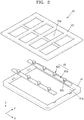
- FIG. 2 is a perspective view of a mask assembly 40 illustrated in FIG. 1 .
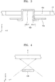
- FIG. 3 is a cross-sectional view illustrating a mask 43 and a stick 42 (support) illustrated in FIG. 2 .
- FIG. 4 is a cross-sectional view illustrating deposition of a deposition material having passed through the stick 42 of FIG. 3 on a display substrate D.
- the apparatus 1 may include a chamber 10, a first support 20, a second support 30, the mask assembly 40, a magnetic force generator 50, a source 60, a pressure adjuster 70, and a vision unit 80.
- the chamber 10 may have a space formed therein, and deposition may be performed in the space.
- An open portion may be formed in the chamber 10, and a gate valve 11 may be arranged in the open portion to close or open the open portion.
- the first support 20 may be arranged in the chamber 10 and may support the display substrate D.
- the first support 20 may have various shapes.
- the first support 20 may be fixed to inside of the chamber 10, and the display substrate D may be seated on the first support 20.
- the first support 20 may include a shuttle that is linearly movable within the chamber 10.
- the first support 20 may have a clamp shape that is arranged in the chamber 10 and holds the display substrate D.
- the first support 20 may be arranged in the chamber 10, and may include, for example, an electrostatic chuck or an adhesive chuck that fixes the display substrate D.
- the first support 20 may include any of devices and structures that support the display substrate D. For convenience of description, a case where the first support 20 is fixed to the inside of the chamber 10 and the display substrate D is safely seated on the first support 20 will now be described in detail.
- the mask assembly 40 may be arranged on the second support 30 and may be supported by the second support 30.
- the second support 30 may adjust a location of the mask assembly 40.
- the second support 30 may raise and lower or rotate the mask assembly 40 by a certain distance, and also may linearly move the mask assembly 40 in a direction.
- the mask assembly 40 may selectively transmit a deposition material.
- the mask assembly 40 may include one or more openings 43a.
- the mask assembly 40 may include an opening 43a that transmits the deposition material.
- a deposition material that has passed through the opening 43a may be deposited on an area of the display substrate D and thus may form a display area.
- the mask assembly 40 may include a plurality of openings 43a that transmit the deposition material.
- the display substrate D may be divided into a plurality of areas, and a deposition material that has passed through each of the openings 43a may be deposited on each of the areas of the display substrate D and thus may form a display area in each of the areas.
- the areas of the display substrate D may be separated from each other after the deposition material is deposited, and thus the single display apparatus may be manufactured.
- the mask assembly 40 includes a plurality of openings 43a will now be described in detail.
- the mask assembly 40 may include a mask frame 41, a stick 42, and a mask 43.
- the mask frame 41 may have a space in a center area thereof.
- the mask frame 41 may have a shape, such as a window frame.
- the mask frame 41 may include seating grooves 41a onto and on which the stick 42 is inserted and seated. Each of the seating grooves 41a may be formed to be indented from an external surface of the mask frame 41, and thus a portion of the stick 42 may be completely inserted onto the seating groove 41a.
- the stick 42 may be arranged on one side of the mask frame 41.
- the stick 42 may include a stick body portion 42a (support body) and a protrusion 42b.
- the stick body portion 42a may extend in a lengthwise direction (for example, an X-axis direction of FIG. 2 (as shown) or a Y-axis direction of FIG. 2 ) of the mask frame 41. At least a portion of the stick body portion 42a may be arranged to be overlapped by the openings 43a. Thus, the stick body portion 42a may be arranged to extend over the openings 43a. An end of the stick body portion 42a may be inserted onto and seated on a seating groove 41a of the mask frame 41.
- the stick body portion 42a may be coupled to the mask frame 41 via, for example, welding or by using a screw, a bolt, or the like.
- the stick body portion 42a may have holes 42c formed therein. The holes 42c may be formed to correspond to protrusions 42b of the stick 42, which will be described below.
- the protrusions 42b may be arranged on the stick body portion 42a such as to protrude toward the display substrate D. In some embodiments, the protrusions 42b may be inserted into the holes 42c and may be connected to the stick body portion 42a. In some embodiments, the protrusions 42b may be integrally formed with the stick body portion 42a or may be formed separate from the stick body portion 42a. For convenience of description, a case where the protrusions 42b and the stick body portion 42a are detachable from each other and are coupled to each other will now be described in detail.
- Each of the protrusions 42b may include a connection portion 42b-2 that is connected to the stick body portion 42a, and a shielding portion 42b-1 that is connected to the connection portion 42b-2.
- the connection portion 42b-2 may be arranged to penetrate a hole 42c of the stick body portion 42a, and a portion of the connection portion 42b-2 may be bent and seated on one side of the stick body portion 42a.
- the bent portion of the connection portion 42b-2 may be fixed to the one side of the stick body portion 42a via, for example, welding or the like.
- the shielding portion 42b-1 may be arranged apart from the stick body portion 42a.
- the shielding portion 42b-1 may be formed to correspond to the shape of a first opening area, which will be described below.
- the shielding portion 42b-1 may be formed to have a circle shape.
- the shielding portion 42b-1 may be formed to have a polygon shape.
- the shielding portion 42b-1 may be formed to correspond to the shape of the first opening area according to the shape of the first opening area.
- One side of the shielding portion 42b-1 (or an end of the protrusion 42b) may be arranged farther from the source 60 than the one side of the stick body portion 42a that contacts the bent portion of the connection portion 42b-2.
- at least a portion of the shielding portion 42b-1 may be arranged within an opening 43a or outside of the opening 43a.
- the shielding portion 42b-1 may be arranged to further protrude toward the display substrate D than the mask 43 protrudes.
- the protrusion 42b may have any shape that is connected to the stick body portion 42a and includes the shielding portion 42b-1 to shield a deposition material to prevent deposition of the deposition material on a portion of the display area of the display substrate D.
- the mask 43 may be arranged on the mask frame 41.
- the mask 43 may include a plurality of openings 43a arranged to correspond to the areas of the display substrate D, respectively.
- Each of the openings 43a may have a shape that corresponds to a display area of each area of the display substrate D.
- the deposition material that has passed through each opening 43a may be deposited on each area of the display substrate D and thus may form the display area.
- One mask 43 or a plurality of masks 43 may be included.
- the plurality of masks 43 may each be formed to have a plate shape and may be arranged on the mask frame 41 to be adjacent to each other. For convenience of description, a case where one mask 43 is formed will now be described in detail.
- the magnetic force generator 50 may be arranged in the chamber 10 and thus may force the mask assembly 40 to be closer toward the display substrate D.
- the magnetic force generator 50 may include at least one of a magnet and an electromagnet that generate magnetic forces.
- the source 60 may store the deposition material, and may sublime or vaporize the deposition material.
- the source 60 may include a heater to heat the deposition material.
- the source 60 may further include a crucible to store the deposition material.
- the source 60 may stand still within the chamber 10 or may linearly move or reciprocate in one direction within the chamber 10.
- the chamber 10 may include a source driving unit that drives the source 60 to linearly move and reciprocate.
- the source driving unit may include a linear motor.
- the vision unit 80 may be arranged within the chamber 10 and may image or photograph at least one of the display substrate D and the mask assembly 40.
- the display substrate D and the mask assembly 40 may be arranged based on data obtained by imaging conducted by the vision unit 80.
- the pressure adjuster 70 may be connected to the chamber 10 and may adjust an internal pressure of the chamber 10.
- the pressure adjuster 70 may include a guide pipe 71 connected to the chamber 10, and a vacuum pump 72 provided on the guide pipe 71 to adjust the internal pressure of the chamber 10. In this case, according to an operation of the vacuum pump 72, gas may be discharged from the chamber 10, or special gas may be supplied into the chamber 10.
- the display substrate D may be arranged within the chamber 10.
- the mask assembly 40 may be arranged within the chamber 10.
- the display substrate D may be arranged on the first support 20, and the mask assembly 40 may be arranged on the second support 30.
- the display substrate D and the mask assembly 40 are arranged as described above, an alignment mark of the display substrate D and an the alignment mark of the mask assembly 40 are photographed by the vision unit 80 and compared with each other, and accordingly the display substrate D and the mask assembly 40 may be aligned.
- the second support 30 may precisely adjust the location of the mask assembly 40.
- the magnetic force generator 50 may apply a magnetic force to the mask assembly 40.
- at least a portion of the stick 42 may be formed of a different material from that used to form the mask 43.
- at least a portion of the stick 42 may include a non-magnetic material and the mask 43 may include a magnetic material.
- at least a portion of the stick 42 may include non-magnetic stainless steel.
- the protrusion 42b of the stick 42 may be formed of a non-magnetic material.
- the mask 43 may include, for example, an iron-nickel alloy (Invar alloy). For convenience of description, a case where the entire stick 42 is formed of stainless steel will now be described in detail.
- the mask assembly 40 may move toward the display substrate D.
- the mask frame 41 may be formed of a magnetic material, the same as or similar to the mask 43.
- the shielding portion 42b-1 may completely adhere to the display substrate D and thus may contact one side of the display substrate D. A portion of the mask 43 may also adhere to the display substrate D.
- the source 60 may operate to supply the deposition material into the chamber 10. At this time, the deposition material may pass through the openings 43a and may be deposited on the display substrate D. In this case, a deposition material that has passed through the openings 43a may be deposited on a display area of the display substrate D.
- a portion of the display substrate D may be exposed via the openings 43a, and the other portion of the display substrate D may not be exposed due to a portion of the mask 43 having no openings 43a formed therein and the shielding portion 42b-1. Accordingly, the deposition material may be deposited on the exposed portion of the display substrate D.
- the deposition material may also be blocked by the stick body portion 42a and the connection portion 42b-2.
- the deposition material sprayed by the source 60 is incident upon the display substrate D at various angles, a portion of the deposition material may be blocked by the stick body portion 42a, but another portion of the deposition material that does not collide with the stick body portion 42a may be deposited on a portion of the display substrate D that is opposite to the stick body portion 42a.
- a deposition material that has avoided the connection portion 42b-2 may be deposited on the display substrate D.
- the deposition material may be deposited on the display area of the display substrate D.
- the stick body portion 42a may be arranged somewhat apart from the display substrate D and thus may not disturb deposition of the deposition material on the portion of the display substrate D that faces the stick body portion 42a.
- the deposition material When the deposition material is deposited as described above, because the shielding portion 42b-1 completely adheres to the display substrate D as described above, the deposition material may not be deposited on a portion of the display substrate D that faces the shielding portion 42b-1. Accordingly, the deposition material may be uniformly deposited on a remaining area of the display area of the display substrate D except for the shielding portion 42b-1.
- the vacuum pump 72 may operate to discharge gas from the chamber 10.
- the mask assembly 40 may be led out to the outside of the chamber 10.
- the vacuum pump 72 may operate to adjust the internal pressure of the chamber 10 to be the same as or similar to an atmospheric pressure.
- the display substrate D may be discharged to the outside of the chamber 10. After a new display substrate D is inserted into the chamber 10, the above-described process may be repeated.
- a hole may be formed in the first opening area via application of laser or mechanical abrasion, and thus a second opening area may be formed.
- the first opening area and the second opening area may be integrally formed with each other and may communicate with each other.
- the second opening area formed later than the first opening area may be formed to be smaller than the first opening area.
- a thin film encapsulation layer may be formed on the display substrate D on which the deposition material has been deposited.
- a display apparatus having an opening area formed therein may be manufactured.
- deposition of the deposition material in the opening area may be prevented by a simple structure, and thus generation of a foreign material during formation of the opening area may be minimized.
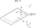
- FIG. 5 is a perspective view of a display apparatus manufactured by the apparatus 1 of FIG. 1 .
- FIG. 6 is a cross-sectional view taken along line VI-VI of FIG. 5 .
- FIG. 7 is a magnified cross-sectional view of an organic light-emitting diode (OLED) illustrated in FIG. 6 .
- OLED organic light-emitting diode
- a display apparatus may include a display panel P and an electronic element corresponding to an opening area RA of the display panel P.
- the opening area RA may be the same as a second opening area RA2.
- a component(s) such as at least one of an input sensing member for sensing a touch input, a reflection preventing member including both a polarizer and a retarder or both a color filter and a black matrix, and a transparent window, may be arranged on the display panel P.
- the electronic element may be arranged within an opening OP that will be described below, or may be arranged outside the opening OP.
- the display panel P may include a substrate 100, a display element layer disposed on the substrate 100 and including display elements, and a thin-film encapsulation layer 300 as an encapsulation member that covers the display element layer.
- the substrate 100 may be formed of a transparent glass material containing SiO 2 as a main component.
- the display element layer includes display elements, such as an OLED arranged in a display area DA.
- the display element layer may include a circuit and wires electrically connected to the OLED.
- the thin-film encapsulation layer 300 may cover the display element layer to thereby prevent infiltration of external moisture or external contaminating materials into the display element layer.
- the thin-film encapsulation layer 300 may include, for example, at least one inorganic encapsulation layer and at least one organic encapsulation layer.
- the display panel P may include an opening OP that corresponds to the opening area RA and penetrates the display panel P. Openings corresponding to respective opening areas RA of the substrate 100, the display element layer, and the thin-film encapsulation layer 300 may form the opening OP of the display panel P.
- the opening area RA may be a location where the electronic element is arranged, and thus the electronic element may be arranged to correspond to respective openings of the substrate 100, the display element layer, and the thin-film encapsulation layer 300.
- the opening of the substrate 100 may be formed to penetrate an upper surface and a lower surface of the substrate 100
- the opening of the display element layer may be formed to penetrate from a lowermost layer of the display element layer to an uppermost layer thereof
- the opening of the thin-film encapsulation layer 300 may be formed to penetrate the thin-film encapsulation layer 300.
- the opening of the thin-film encapsulation layer 300 may be formed by forming the opening of the display element layer and then forming the thin-film encapsulation layer 300 on the inner surface of the opening of the display element layer.
- the electronic element may be an electronic element that uses light and/or sound.
- the electronic element may include, for example, a sensor that receives and uses light, like an infrared sensor, a camera that receives light and captures an image, a sensor that outputs and senses light or sound to measure a distance or recognize a fingerprint or the like, a small lamp that outputs light, or a speaker that outputs sound.
- An electronic element using light may use light in various wavelength bands, such as visible light, infrared light, and ultraviolet light.
- the opening area RA may be understood as a transmission area capable of transmitting light or/and sound that is output from the electronic element to the outside or travels from the outside toward the electronic element. For example, when a portion of the display panel P corresponding to the opening area RA is completely removed, for example, when the opening OP penetrates the display panel P, light or sound output or received by the electronic element may be more effectively used.
- the display element layer and the thin-film encapsulation layer 300 may respectively include openings corresponding to the opening area RA, and the substrate 100 may not include openings.
- the substrate 100 does not include openings
- the display element layer and the thin-film encapsulation layer 300 may include openings, respectively, and thus transmittance of light and/or sound that the electronic element uses may be secured.
- a light transmittance in the opening area RA of the display panel P may be about 50% or greater, 70% or greater, 75% or greater, 80% or greater, 85% or greater, or 90% or greater.
- the substrate 100 of the display panel P may include polymer resin.
- the substrate 100 may secure greater flexibility than a substrate formed of a glass material.
- the substrate 100 may include a first base layer, a first inorganic layer, a second base layer, and a second inorganic layer sequentially stacked thereon.
- the first and second base layers may include transparent polymer resin.
- the transparent polymer resin may be, for example, polyethersulphone (PES), polyacrylate (PAR), polyetherimide (PEI), polyethylene naphthalate (PEN), polyethyelene terephthalate (PET), polyphenylene sulfide (PPS), polyallylate, polyimide (PI), cellulose triacetate (TAC), or cellulose acetate propionate (CAP).
- PES polyethersulphone
- PAR polyacrylate
- PEI polyetherimide
- PEN polyethylene naphthalate
- PET polyethyelene terephthalate
- PPS polyphenylene sulfide
- PI polyimide
- TAC cellulose triacetate
- CAP cellulose acetate propionate
- Each of the first and second inorganic layers may be a barrier layer that prevents infiltration of external foreign materials, and thus may be a single layer or multiple layers including an inorganic material, such as SiNx and/or SiOx.
- the substrate 100 including polymer resin may include an opening corresponding to the opening area RA, or may not include openings. However, as described above, the display element layer and the thin-film encapsulation layer 300 may include openings, respectively.
- the display panel P includes a plurality of pixels arranged in the display area DA.
- Each of the pixels may include, for example, an OLED.
- Each of the pixels may emit, for example, red light, green light, blue light, or white light via the OLED.
- a first non-display area NDA1 surrounds the opening area RA.
- the first non-display area NDA1 may be an area where a display element, such as an OLED that emits light, is not arranged.
- a scan driver that provides a scan signal to each of the pixels
- a data driver that provides a data signal to each of the pixels
- a main power wire for providing first and second power supply voltages may be arranged.
- a buffer layer 201 to prevent infiltration of impurities into a semiconductor layer of a thin film transistor (TFT) may be arranged on the substrate 100.
- the buffer layer 201 may include, for example, an inorganic insulating material, such as silicon nitride or silicon oxide, and may be a single layer or multiple layers including the inorganic insulating material.
- the second inorganic layer may be understood as a portion of the buffer layer 201 having a multi-layered structure.
- a pixel circuit PC including a TFT and a storage capacitor Cst may be arranged on the buffer layer 201.
- the TFT may include a semiconductor layer ACT, a gate electrode GE, a source electrode SE, and a drain electrode DE.
- the TFT may be a driving TFT.
- the TFT is a top gate type in which the gate electrode GE is arranged on the semiconductor layer ACT with a gate insulating layer 203 therebetween.
- the TFT may be a bottom gate type.
- the semiconductor layer ACT may include, for example, polysilicon. In another example embodiment, the semiconductor layer ACT may include, for example, amorphous silicon, an oxide semiconductor, or an organic semiconductor.
- the gate electrode GE2 may include, for example, a low resistance metal material.
- the gate electrode GE may include, for example, a conductive material including, for example, molybdenum (Mo), aluminum (Al), copper (Cu), and titanium (Ti), and may be formed as a multi-layer or single layer including the aforementioned materials.
- the gate insulating layer 203 may be interposed between the semiconductor layer ACT and the gate electrode GE and may include, for example, an inorganic insulating material, such as silicon oxide, silicon nitride, silicon oxynitride, aluminum oxide, titanium oxide, tantalum oxide, or hafnium oxide.
- an inorganic insulating material such as silicon oxide, silicon nitride, silicon oxynitride, aluminum oxide, titanium oxide, tantalum oxide, or hafnium oxide.
- the source electrode SE and the drain electrode DE may include, for example, a highly conductive material.
- Each of the source electrode SE and the drain electrode DE may include, for example, a conductive material including Mo, Al, Cu, and/or Ti, and may be a multi-layer or single layer including the aforementioned materials.
- each of the source electrode SE and the drain electrode DE may be formed as a multi-layer of Ti/Al/Ti.
- the storage capacitor Cst includes a lower electrode CE1 and an upper electrode CE2 with a first interlayer insulating layer 205 therebetween.
- the lower electrode CE1 and the upper electrode CE2 overlap each other.
- the storage capacitor Cst may be overlapped with the TFT.
- FIG. 6 illustrates a case where the gate electrode GE of the TFT is the lower electrode CE1 of the storage capacitor Cst, but embodiments of the present disclosure are not limited thereto. According to another example embodiment, the storage capacitor Cst may not be overlapped with the TFT.
- the storage capacitor Cst may be covered with a second interlayer insulating layer 207.
- the first and second interlayer insulating layers 205 and 207 may include, for example, an inorganic insulating material, such as silicon oxide, silicon nitride, silicon oxynitride, aluminum oxide, titanium oxide, tantalum oxide, or hafnium oxide.
- an inorganic insulating material such as silicon oxide, silicon nitride, silicon oxynitride, aluminum oxide, titanium oxide, tantalum oxide, or hafnium oxide.
- the pixel circuit PC including the TFT and the storage capacitor Cst may be covered with a first insulating layer 209.
- the first insulating layer 209 may serve as a planarization insulating layer, and may include, for example, an organic insulating material, such as a polymer (such as polymethyl methacrylate (PMMA) or polystyrene (PS)), a polymer derivative having a phenol-based group, an acryl-based polymer, an imide-based polymer, an acryl ether-based polymer, an amide-based polymer, a fluorine-based polymer, a p-xylene-based polymer, a vinyl alcohol-based polymer, a blend thereof, or the like.
- the first insulating layer 209 may include polyimide.
- the first insulating layer 209 may have a thickness of about 1.7 ⁇ m to about 2.4 ⁇ m.
- the OLED may be disposed on the first insulating layer 209.
- a pixel electrode 221 of the OLED may be arranged on the first insulating layer 209 and may be connected to the pixel circuit PC via a contact hole of the first insulating layer 209.
- the pixel electrode 221 may include conductive oxide, such as indium tin oxide (ITO), indium zinc oxide (IZO), zinc oxide (ZnO), indium oxide (In 2 O 3 ), indium gallium oxide (IGO), or aluminum zinc oxide (AZO).
- the pixel electrode 221 may include, for example, a reflection layer including silver (Ag), magnesium (Mg), aluminum (Al), platinum (Pt), palladium (Pd), gold (Au), nickel (Ni), neodymium (Nd), iridium (Ir), chromium (Cr), or a compound of these materials.
- the pixel electrode 221 may further include, for example, a film formed of ITO, IZO, ZnO, or In 2 O 3 above/below the reflection layer.
- a second insulating layer 211 includes an opening via which an upper surface of the pixel electrode 221 is exposed, and covers an edge of the pixel electrode 221.
- the second insulating layer 211 may include, for example, an inorganic insulating material.
- the second insulating layer 211 may include silicon oxide and/or silicon nitride and may be a single layer or a multi-layer.
- a thickness of the second insulating layer 211 may be less than that of the first insulating layer 209.
- An intermediate layer 222 may include an emission layer.
- the emission layer may include, for example, a low molecular or high molecular organic material that emits light of a certain color.
- the intermediate layer 222 may further include a first functional layer 222A arranged below an emission layer 222B, and/or a second functional layer 222C arranged above the emission layer 222B.
- the first functional layer 222A may be a single layer or a multi-layer.
- the first functional layer 222A is a hole transport layer (HTL) having a single-layer structure, and may be formed of poly-(3,4)-ethylene-dihydroxy thiophene (PEDOT) or polyaniline (PANI).
- HTL hole transport layer
- PEDOT poly-(3,4)-ethylene-dihydroxy thiophene
- PANI polyaniline
- the first functional layer 222A may include a hole injection (HIL) and an HTL.
- the second functional layer 222C may be formed to improve the characteristics of the OLED.
- the second functional layer 222C may be a single layer or a multi-layer.
- the second functional layer 222C may include an electron transport layer (ETL), and/or an electron injection layer (EIL).
- ETL electron transport layer
- EIL electron injection layer
- Some of a plurality of layers that constitute the intermediate layer 222 may be arranged not only in the display area DA but also in the first non-display area NDA1.
- An opposite electrode 223 may be arranged to face the pixel electrode 221, with the intermediate layer 222 therebetween.
- the opposite electrode 223 may be formed of a conductive material having a low work function.
- the opposite electrode 223 may include a (semi)transparent layer including silver (Ag), magnesium (Mg), aluminum (Al), platinum (Pt), palladium (Pd), gold (Au), nickel (Ni), neodymium (Nd), iridium (Ir), chromium (Cr), lithium (Li), calcium (Ca) or an alloy of these materials.
- the opposite electrode 223 may further include a layer, such as ITO, IZO, ZnO, or In 2 O 3 , on the (semi)transparent layer including any of the above-described materials.
- the opposite electrode 223 may be arranged not only in the display area DA but also in the first non-display area NDA1. According to another example embodiment, the opposite electrode 223 may be arranged only in the display area DA. For convenience of description, a case where the opposite electrode 223 is arranged only in the display area DA will now be described in detail.
- the OLED may be covered with the thin-film encapsulation layer 300.
- the thin-film encapsulation layer 300 may include at least one organic encapsulation layer and at least one inorganic encapsulation layer.
- the thin-film encapsulation layer 300 as shown includes first and second inorganic encapsulation layers 310 and 330 and an organic encapsulation layer 320 therebetween in FIG. 6 , a stacking order of the first and second inorganic encapsulation layers 310 and 330 and the organic encapsulation layer 320 and the numbers of inorganic encapsulation layers and organic encapsulation layers may be changed.
- the first and second inorganic encapsulation layers 310 and 330 may include, for example, an inorganic insulating material of at least one of aluminum oxide, titanium oxide, tantalum oxide, hafnium oxide, zinc oxide, silicon oxide, silicon nitride, and silicon oxynitride, and may be formed via chemical vapor deposition (CVD) or the like.
- the organic encapsulation layer 320 may include, for example, a polymer-based material. Examples of the polymer-based material include acrylic resin, epoxy resin, polyimide, and polyethylene.
- Data lines DL may alternate with each other, with an insulating layer therebetween. Neighboring data lines DL may be arranged below and above the insulating layer (for example, the second interlayer insulating layer 207), respectively.
- a display apparatus as described above may be manufactured by using the apparatus 1 and the method of manufacturing a display apparatus described above with reference to FIGS. 1 through 4 .
- the above-described mask assembly (40 of FIG. 1 ) may be used.
- the deposition material may be deposited on the display substrate D via the mask assembly, as described above.
- the display substrate D may include the substrate 100, the buffer layer 201, the gate insulating layer 203, the first interlayer insulating layer 205, the TFT, the second interlayer insulating layer 207, the first insulating layer 209, the second insulating layer 211, and the pixel electrode 221.
- the display substrate D may further include the first functional layer 222A and the emission layer 222B in addition to the above-described layers.
- at least one of the first functional layer 222A and the second functional layer 222C may be deposited via the above-described apparatus 1.
- the second functional layer 222C is formed on the display substrate D will now be described in detail.
- the deposition material may be deposited on the display substrate D by using the mask assembly, as described above.
- the second functional layer 222C may be blocked by a shielding portion and thus may not be formed in the opening area RA. According to another example embodiment, the second functional layer 222C may not be formed even in the first non-display area NDA1 surrounding the opening area RA, due to the shielding portion.
- a deposition material that has passed through an opening of a mask may be deposited in the display area DA except for the shielding portion, and thus the second functional layer 222C may be formed.
- the opposite electrode 223 may be formed on the second functional layer 222C.
- the opposite electrode 223 may be formed, similar to the formation of the second functional layer 222C.
- the first opening area RA1 not including the first functional layer 222A, the second functional layer 222C, and the opposite electrode 223 may be formed in the opening area RA.
- the thin-film encapsulation layer 300 may be formed on the opposite electrode 223, thereby manufacturing the display panel P.
- at least a portion of the thin-film encapsulation layer 300 may be arranged on an inner surface of the first opening area RA1 and thus may shield at least a portion of the first opening area RA1.
- the second opening area RA2 may be formed by irradiating a laser to the first opening area RA1 or mechanically abrading the first opening area RA1. In this way, the opening area RA may be completed. In this case, the second opening area RA2 may be formed to penetrate the substrate 100 and other layers.
- the second opening area RA2 may be formed by irradiating a laser to the first opening area RA1 or mechanically abrading the first opening area RA1.
- the thin-film encapsulation layer 300 may be formed.
- at least a portion of the thin-film encapsulation layer 300 may be formed on the inner surface of the opening OP, and thus external moisture or oxygen may be prevented from infiltrating into each layer of the display panel P.
- the display apparatus may minimize gas or a foreign material that is generated due to use of laser or the like during formation of the second opening area RA2, and thermal deformation of the first and second functional layers 222A and 222C due to application of heat thereto may be prevented.
- FIG. 8 is a cross-sectional view of a stick of a mask assembly in an apparatus for manufacturing a display apparatus, according to another example embodiment.
- a description of an apparatus for manufacturing a display apparatus may be similar to that of the apparatus 1 of FIGS. 1 through 4 .
- a description of a mask assembly is similar to that of the mask assembly 40 of FIGS. 1 through 4 .
- a stick 42' (support) may be formed to have various shapes in various embodiments.
- the stick 42' may include a stick body portion 42a' and a protrusion 42b'.
- the stick body portion 42a' and the protrusion 42b' may be integrally formed with each other. In this case, after the stick body portion 42a' and the protrusion 42b' may be formed in a straight line, and then the straight line may be bent to form the protrusion 42b'.
- the stick body portion 42a' and the protrusion 42b' may be formed the same as or similar to descriptions given with reference to FIGS. 1 through 4 .
- FIG. 9 is a cross-sectional view of a stick of a mask assembly in an apparatus for manufacturing a display apparatus, according to another example embodiment.
- a description of an apparatus for manufacturing a display apparatus may be similar to that of the apparatus 1 of FIGS. 1 through 4 .
- a description of a mask assembly may be similar to that of the mask assembly 40 of FIGS. 1 through 4 .
- a stick 42" (support) may include a stick body portion 42a" and a protrusion 42b".
- the stick body portion 42a" and the protrusion 42b" may be formed to be separated from each other.
- the protrusions 42b" may be arranged on one side of the stick body portion 42a" that faces the display substrate D. In this case, the protrusion 42b" may protrude from the stick body portion 42a" toward the display substrate D.
- a width of a connection portion 42b"-2 of the protrusion 42b" may be less than that of a shielding portion 42b"-1 of the protrusion 42b".
- a width of the stick body portion 42a" may also be less than that of the shielding portion 42b"-1.
- the width of the stick body portion 42a" and that of the connection portion 42b"-2 may be equal to each other.
- the width of the connection portion 42b"-2 may be measured in a Y-axis direction of FIG. 8
- the width of the stick body portion 42a" may be measured in an X-axis direction of FIG. 8
- the width of the shielding portion 42b"-1 may be measured in the X-axis or Y-axis direction of FIG. 9 .
- the stick body portion 42a" and the protrusion 42b" may be similar to those described above with reference to FIGS. 1 through 4 .
- FIG. 10 is a cross-sectional view of a stick of a mask assembly in an apparatus for manufacturing a display apparatus, according to another example embodiment.
- a description of an apparatus for manufacturing a display apparatus may be similar to that of the apparatus 1 of FIGS. 1 through 4 .
- a description of a mask assembly may be similar to that of the mask assembly 40 of FIGS. 1 through 4 .
- a stick 42"' may include a stick body portion 42a"' and a protrusion 42b"'.
- the stick body portion 42a"' and the protrusion 42b"' may be separated from each other or may be integrally formed with each other.
- the stick body portion 42a"' and the protrusion 42b"' are integrally formed with each other, they may be manufactured by processing a base member via, for example, etching or the like.
- the stick body portion 42a"' and the protrusion 42b"' when the stick body portion 42a"' and the protrusion 42b"' are formed to be separated from each other, they may be manufactured independently and may be connected to each other via, for example, welding or the like.
- the protrusion 42b"' may include a connection portion 42b"'-2 and a shielding portion 42b"'-1.
- the connection portion 42b"'-2 may be formed to have an H shape.
- the connection portion 42b"'-2 may be connected to a center of the shielding portion 42b"'-1 to thereby connect the shielding portion 42b"'-1 to the stick body portion 42a"'.
- the shielding portion 42b"'-1 may be formed to have various shapes. In this case, as described above, the shielding portion 42b"'-1 may have various shapes according to the shape of an opening area to be formed.
- Embodiments of the invention may provide a mask assembly, comprising: a mask frame; a mask on the mask frame and including at least one opening through which a deposition material can pass; and a support arranged on the mask frame and extending over a portion of the opening, the support including: a support body portion connected to the mask frame and extending over the portion of the opening; and a protrusion protruding from the support body portion toward the opening.
- the mask assembly may be use to form a display substrate, and the protrusion may be in contact with a display substrate.
- Embodiments of the invention may provide an apparatus for manufacturing a display apparatus, the apparatus comprising: a chamber to accommodate a display substrate; a mask assembly positioned to face the display substrate; and a source facing the mask assembly and configured to supply a deposition material to the display substrate.
- Embodiments of the invention may provide a method of manufacturing a display apparatus, the method comprising: arranging a display substrate and a mask assembly within a chamber; aligning the display substrate with the mask assembly; and supplying a deposition material from a source, passing the deposition material through the mask assembly, and supplying the deposition material to the display substrate, wherein the deposition material is blocked by a blocking member while passing through an opening of the mask assembly to form an opening area in the display substrate, and is deposited on a display area of the display substrate except for the opening area.
- the blocking member may be arranged in the region of the opening of the mask assembly.
- the blocking member may be a protrusion in contact with the display substrate.
- the mask assembly may include a mask frame; a mask on the mask frame and including the opening through which the deposition material passes; and a support arranged on the mask frame and extending over the opening, and the support includes: a support body portion connected to the mask frame and extending over the opening; and a protrusion protruding from the support body portion toward the opening.
- the support may provide the blocking member.
- a display apparatus may be formed to have an opening in a display area.
- gas or a foreign material may be generated during removal of some layers.
- a foreign material may be generated or excessive energy may be used. Accordingly, an organic light-emitting device around the hole may be damaged.
- embodiments may provide for forming a display apparatus including an opening while minimizing generation of gas or a foreign material.
- various electronic elements may be arranged by including an opening.
- generation of gas or foreign materials during formation of the opening may be minimized.
- the opening may be formed via a simple structure.
Landscapes
- Chemical & Material Sciences (AREA)
- Engineering & Computer Science (AREA)
- Manufacturing & Machinery (AREA)
- Chemical Kinetics & Catalysis (AREA)
- Materials Engineering (AREA)
- Mechanical Engineering (AREA)
- Metallurgy (AREA)
- Organic Chemistry (AREA)
- Electroluminescent Light Sources (AREA)
- Physical Vapour Deposition (AREA)
Abstract
Description
- Embodiments relate to a mask assembly, and an apparatus and method for manufacturing a display apparatus including the mask assembly.
- Applications of display apparatuses have diversified. Additionally, due to their relatively small thickness and light weight, their range of applications has increased.
- The area occupied by display areas of display apparatuses has been increased, and also various functions that may be applied or linked to a display apparatus have been added.
- Embodiments are directed to a mask assembly, including a mask frame, a mask on the mask frame and including at least one opening through which a deposition material can pass, and a stick on the mask frame and extending over the opening, the stick including a stick body portion connected to the mask frame and extending over the opening, and a protrusion protruding from the stick body portion toward the opening.
- The stick body portion and the protrusion may be separable from each other.
- The protrusion may include a connection portion connected to the stick body portion, and a shielding portion connected to the connection portion and configured to shield the deposition material.
- An end of the protrusion may be arranged farther from a source, which is configured to spray the deposition material, than one side of the mask that faces the source.
- The mask and at least a portion of the stick may include different materials from each other.
- At least a portion of the stick may be a non-magnetic material.
- A hole may be in a portion of the stick body portion that corresponds to the protrusion.
- The mask frame, the stick, and the mask may be sequentially stacked.
- Embodiments are also directed to an apparatus for manufacturing a display apparatus, the apparatus including a chamber to accommodate a display substrate, a mask assembly positioned to face the display substrate, and a source facing the mask assembly and configured to supply a deposition material to the display substrate. The mask assembly may include a mask frame, a mask on the mask frame and including at least one opening through which the deposition material can pass, and a stick on the mask frame and extending over the opening, and the stick may include a stick body portion connected to the mask frame and extending over the opening, and a protrusion protruding from the stick body portion toward the opening.
- The stick body portion and the protrusion may be separable from each other.
- The protrusion may include a connection portion connected to the stick body portion, and a shielding portion connected to the connection portion and configured to shield the deposition material.
- An end of the protrusion may be arranged farther from a source, which is configured to spray the deposition material, than one side of the mask that faces the source.
- The mask and at least a portion of the stick may include different materials from each other.
- At least a portion of the stick may be a non-magnetic material.
- A hole may be in a portion of the stick body portion that corresponds to the protrusion.
- The mask frame, the stick, and the mask may be sequentially stacked.
- Embodiments are also directed to a method of manufacturing a display apparatus, the method including arranging a display substrate and a mask assembly within a chamber, aligning the display substrate with the mask assembly, and supplying a deposition material from a source, passing the deposition material through the mask assembly, and supplying the deposition material to the display substrate. The deposition material may be blocked by a certain area while passing through an opening of the mask assembly to form an opening area in the display substrate, and is deposited on a display area of the display substrate except for the opening area.
- The mask assembly may include a protrusion that corresponds to the opening area and protrudes toward the display substrate.
- The protrusion may be in contact with the display substrate.
- The deposition material may forms at least one of at least a portion of an intermediate layer of the display substrate, and an opposite electrode.
- Embodiments are also directed to a method of manufacturing a display apparatus, the method including arranging a display substrate and a mask assembly within a chamber, aligning the display substrate with the mask assembly, and supplying a deposition material from a source, passing the deposition material through the mask assembly, and supplying the deposition material to the display substrate. The mask assembly may include a mask frame, a mask on the mask frame and including at least one opening through which the deposition material passes, and a stick on the mask frame and extending over the opening, and the stick may include a stick body portion connected to the mask frame and extending over the opening, and a protrusion protruding from the stick body portion toward the opening.
- An end of the protrusion may be arranged farther from the source than one side of the mask that faces the source.
- The mask and at least a portion of the stick may include different materials.
- At least a portion of the stick may be a non-magnetic material.
- According to an aspect, there is provided a mask assembly as set out in
claim 1. Additional features of this aspect are set out inclaims 2 to 8. According to an aspect, there is provided an apparatus for manufacturing a display apparatus as set out in claim 9. According to an aspect, there is provided method for manufacturing a display apparatus as set out inclaim 10. Additional features of this aspect are set out inclaims 11 to 15. - Features will become apparent to those of skill in the art by describing in detail example embodiments with reference to the attached drawings in which:
-
FIG. 1 illustrates a cross-sectional view of an apparatus for manufacturing a display apparatus, according to an example embodiment; -
FIG. 2 illustrates a perspective view of a mask assembly illustrated inFIG. 1 ; -
FIG. 3 illustrates a cross-sectional view of a mask and a stick illustrated inFIG. 2 ; -
FIG. 4 illustrates a cross-sectional view of deposition, onto a display substrate, of a deposition material having passed through the stick ofFIG. 3 ; -
FIG. 5 illustrates a perspective view of a display apparatus manufactured by the apparatus ofFIG. 1 ; -
FIG. 6 illustrates a cross-sectional view taken along line VI-VI ofFIG. 5 ; -
FIG. 7 illustrates a magnified cross-sectional view of an organic light-emitting diode (OLED) illustrated inFIG. 6 ; -
FIG. 8 illustrates a cross-sectional view of a stick of a mask assembly in an apparatus for manufacturing a display apparatus, according to another example embodiment; -
FIG. 9 illustrates a cross-sectional view of a stick of a mask assembly in an apparatus for manufacturing a display apparatus, according to another example embodiment; and -
FIG. 10 illustrates a cross-sectional view of a stick of a mask assembly in an apparatus for manufacturing a display apparatus, according to another example embodiment. - Example embodiments will now be described more fully hereinafter with reference to the accompanying drawings; however, they may be embodied in different forms and should not be construed as limited to the embodiments set forth herein. Rather, these embodiments are provided so that this disclosure will be thorough and complete, and will fully convey example implementations to those skilled in the art. In the drawing figures, the dimensions of layers and regions may be exaggerated for clarity of illustration. Like reference numerals refer to like elements throughout.
- It will be understood that although the terms "first", "second", etc. may be used herein to describe various components, these components should not be limited by these terms. These components are only used to distinguish one component from another.
- As used herein, the singular forms "a", "an" and "the" are intended to include the plural forms as well, unless the context clearly indicates otherwise.
- It will be further understood that the terms "comprises" and/or "comprising" used herein specify the presence of stated features or components, but do not preclude the presence or addition of one or more other features or components.
- It will be understood that when a layer, region, or component is referred to as being "formed on" another layer, region, or component, it can be directly or indirectly formed on the other layer, region, or component. That is, for example, intervening layers, regions, or components may be present.
- When a certain embodiment may be implemented differently, a specific process order may be performed differently from the described order. For example, two consecutively described processes may be performed substantially at the same time or performed in an order opposite to the described order.
- It will also be understood that when a layer, region, or component is referred to as being "connected" or "coupled" to another layer, region, or component, it can be directly connected or coupled to the other layer, region, or component or intervening layers, regions, or components may be present. For example, when a layer, region, or component is referred to as being "electrically connected" or "electrically coupled" to another layer, region, or component, it can be directly electrically connected or coupled to the other layer, region, or component or intervening layers, regions, or components may be present.
-
FIG. 1 is a cross-sectional view of anapparatus 1 for manufacturing a display apparatus, according to an example embodiment.FIG. 2 is a perspective view of amask assembly 40 illustrated inFIG. 1 .FIG. 3 is a cross-sectional view illustrating amask 43 and a stick 42 (support) illustrated inFIG. 2 .FIG. 4 is a cross-sectional view illustrating deposition of a deposition material having passed through thestick 42 ofFIG. 3 on a display substrate D. - Referring to
FIGS. 1 through 4 , theapparatus 1 may include achamber 10, a first support 20, asecond support 30, themask assembly 40, amagnetic force generator 50, asource 60, apressure adjuster 70, and avision unit 80. - The
chamber 10 may have a space formed therein, and deposition may be performed in the space. An open portion may be formed in thechamber 10, and agate valve 11 may be arranged in the open portion to close or open the open portion. - The first support 20 may be arranged in the
chamber 10 and may support the display substrate D. The first support 20 may have various shapes. For example, the first support 20 may be fixed to inside of thechamber 10, and the display substrate D may be seated on the first support 20. According to another example embodiment, the first support 20 may include a shuttle that is linearly movable within thechamber 10. According to another example embodiment, the first support 20 may have a clamp shape that is arranged in thechamber 10 and holds the display substrate D. According to another example embodiment, the first support 20 may be arranged in thechamber 10, and may include, for example, an electrostatic chuck or an adhesive chuck that fixes the display substrate D. The first support 20 may include any of devices and structures that support the display substrate D. For convenience of description, a case where the first support 20 is fixed to the inside of thechamber 10 and the display substrate D is safely seated on the first support 20 will now be described in detail. - The
mask assembly 40 may be arranged on thesecond support 30 and may be supported by thesecond support 30. In this case, thesecond support 30 may adjust a location of themask assembly 40. For example, thesecond support 30 may raise and lower or rotate themask assembly 40 by a certain distance, and also may linearly move themask assembly 40 in a direction. - The
mask assembly 40 may selectively transmit a deposition material. Themask assembly 40 may include one ormore openings 43a. For example, according to an example embodiment, themask assembly 40 may include anopening 43a that transmits the deposition material. A deposition material that has passed through theopening 43a may be deposited on an area of the display substrate D and thus may form a display area. According to another example embodiment, themask assembly 40 may include a plurality ofopenings 43a that transmit the deposition material. In this case, the display substrate D may be divided into a plurality of areas, and a deposition material that has passed through each of theopenings 43a may be deposited on each of the areas of the display substrate D and thus may form a display area in each of the areas. For example, in this case, the areas of the display substrate D may be separated from each other after the deposition material is deposited, and thus the single display apparatus may be manufactured. For convenience of description, a case where themask assembly 40 includes a plurality ofopenings 43a will now be described in detail. - The
mask assembly 40 may include amask frame 41, astick 42, and amask 43. Themask frame 41 may have a space in a center area thereof. Themask frame 41 may have a shape, such as a window frame. Themask frame 41 may includeseating grooves 41a onto and on which thestick 42 is inserted and seated. Each of theseating grooves 41a may be formed to be indented from an external surface of themask frame 41, and thus a portion of thestick 42 may be completely inserted onto theseating groove 41a. - The
stick 42 may be arranged on one side of themask frame 41. Thestick 42 may include astick body portion 42a (support body) and aprotrusion 42b. - The
stick body portion 42a may extend in a lengthwise direction (for example, an X-axis direction ofFIG. 2 (as shown) or a Y-axis direction ofFIG. 2 ) of themask frame 41. At least a portion of thestick body portion 42a may be arranged to be overlapped by theopenings 43a. Thus, thestick body portion 42a may be arranged to extend over theopenings 43a. An end of thestick body portion 42a may be inserted onto and seated on aseating groove 41a of themask frame 41. Thestick body portion 42a may be coupled to themask frame 41 via, for example, welding or by using a screw, a bolt, or the like. Thestick body portion 42a may haveholes 42c formed therein. Theholes 42c may be formed to correspond toprotrusions 42b of thestick 42, which will be described below. - The
protrusions 42b may be arranged on thestick body portion 42a such as to protrude toward the display substrate D. In some embodiments, theprotrusions 42b may be inserted into theholes 42c and may be connected to thestick body portion 42a. In some embodiments, theprotrusions 42b may be integrally formed with thestick body portion 42a or may be formed separate from thestick body portion 42a. For convenience of description, a case where theprotrusions 42b and thestick body portion 42a are detachable from each other and are coupled to each other will now be described in detail. Each of theprotrusions 42b may include aconnection portion 42b-2 that is connected to thestick body portion 42a, and a shieldingportion 42b-1 that is connected to theconnection portion 42b-2. Theconnection portion 42b-2 may be arranged to penetrate ahole 42c of thestick body portion 42a, and a portion of theconnection portion 42b-2 may be bent and seated on one side of thestick body portion 42a. The bent portion of theconnection portion 42b-2 may be fixed to the one side of thestick body portion 42a via, for example, welding or the like. The shieldingportion 42b-1 may be arranged apart from thestick body portion 42a. The shieldingportion 42b-1 may be formed to correspond to the shape of a first opening area, which will be described below. For example, when the first opening area to be formed is circular, the shieldingportion 42b-1 may be formed to have a circle shape. According to another example embodiment, when the first opening area to be formed is polygonal, the shieldingportion 42b-1 may be formed to have a polygon shape. The shieldingportion 42b-1 may be formed to correspond to the shape of the first opening area according to the shape of the first opening area. One side of the shieldingportion 42b-1 (or an end of theprotrusion 42b) may be arranged farther from thesource 60 than the one side of thestick body portion 42a that contacts the bent portion of theconnection portion 42b-2. In this case, at least a portion of the shieldingportion 42b-1 may be arranged within anopening 43a or outside of theopening 43a. For example, the shieldingportion 42b-1 may be arranged to further protrude toward the display substrate D than themask 43 protrudes. - The
protrusion 42b may have any shape that is connected to thestick body portion 42a and includes the shieldingportion 42b-1 to shield a deposition material to prevent deposition of the deposition material on a portion of the display area of the display substrate D. - The
mask 43 may be arranged on themask frame 41. Themask 43 may include a plurality ofopenings 43a arranged to correspond to the areas of the display substrate D, respectively. Each of theopenings 43a may have a shape that corresponds to a display area of each area of the display substrate D. The deposition material that has passed through eachopening 43a may be deposited on each area of the display substrate D and thus may form the display area. - One
mask 43 or a plurality ofmasks 43 may be included. When a plurality ofmasks 43 is included, the plurality ofmasks 43 may each be formed to have a plate shape and may be arranged on themask frame 41 to be adjacent to each other. For convenience of description, a case where onemask 43 is formed will now be described in detail. - The
magnetic force generator 50 may be arranged in thechamber 10 and thus may force themask assembly 40 to be closer toward the display substrate D. In this case, themagnetic force generator 50 may include at least one of a magnet and an electromagnet that generate magnetic forces. - The
source 60 may store the deposition material, and may sublime or vaporize the deposition material. Thesource 60 may include a heater to heat the deposition material. Thesource 60 may further include a crucible to store the deposition material. Thesource 60 may stand still within thechamber 10 or may linearly move or reciprocate in one direction within thechamber 10. When thesource 60 moves, thechamber 10 may include a source driving unit that drives thesource 60 to linearly move and reciprocate. In this case, the source driving unit may include a linear motor. For convenience of description, a case where thesource 60 is fixed within thechamber 10 will now be described in detail. - The
vision unit 80 may be arranged within thechamber 10 and may image or photograph at least one of the display substrate D and themask assembly 40. The display substrate D and themask assembly 40 may be arranged based on data obtained by imaging conducted by thevision unit 80. - The
pressure adjuster 70 may be connected to thechamber 10 and may adjust an internal pressure of thechamber 10. Thepressure adjuster 70 may include a guide pipe 71 connected to thechamber 10, and a vacuum pump 72 provided on the guide pipe 71 to adjust the internal pressure of thechamber 10. In this case, according to an operation of the vacuum pump 72, gas may be discharged from thechamber 10, or special gas may be supplied into thechamber 10. - When the
apparatus 1 manufactures a display apparatus, the display substrate D may be arranged within thechamber 10. In this case, themask assembly 40 may be arranged within thechamber 10. - The display substrate D may be arranged on the first support 20, and the
mask assembly 40 may be arranged on thesecond support 30. - When the display substrate D and the
mask assembly 40 are arranged as described above, an alignment mark of the display substrate D and an the alignment mark of themask assembly 40 are photographed by thevision unit 80 and compared with each other, and accordingly the display substrate D and themask assembly 40 may be aligned. In this case, thesecond support 30 may precisely adjust the location of themask assembly 40. - The
magnetic force generator 50 may apply a magnetic force to themask assembly 40. In this case, at least a portion of thestick 42 may be formed of a different material from that used to form themask 43. For example, at least a portion of thestick 42 may include a non-magnetic material and themask 43 may include a magnetic material. For example, at least a portion of thestick 42 may include non-magnetic stainless steel. For example, theprotrusion 42b of thestick 42 may be formed of a non-magnetic material. Themask 43 may include, for example, an iron-nickel alloy (Invar alloy). For convenience of description, a case where theentire stick 42 is formed of stainless steel will now be described in detail. - When the
magnetic force generator 50 applies a magnetic force as described above, themask assembly 40 may move toward the display substrate D. In this case, themask frame 41 may be formed of a magnetic material, the same as or similar to themask 43. - The shielding
portion 42b-1 may completely adhere to the display substrate D and thus may contact one side of the display substrate D. A portion of themask 43 may also adhere to the display substrate D. - The
source 60 may operate to supply the deposition material into thechamber 10. At this time, the deposition material may pass through theopenings 43a and may be deposited on the display substrate D. In this case, a deposition material that has passed through theopenings 43a may be deposited on a display area of the display substrate D. - In the above case, a portion of the display substrate D may be exposed via the
openings 43a, and the other portion of the display substrate D may not be exposed due to a portion of themask 43 having noopenings 43a formed therein and the shieldingportion 42b-1. Accordingly, the deposition material may be deposited on the exposed portion of the display substrate D. - While the deposition material is being deposited as described above, the deposition material may also be blocked by the
stick body portion 42a and theconnection portion 42b-2. However, because the deposition material sprayed by thesource 60 is incident upon the display substrate D at various angles, a portion of the deposition material may be blocked by thestick body portion 42a, but another portion of the deposition material that does not collide with thestick body portion 42a may be deposited on a portion of the display substrate D that is opposite to thestick body portion 42a. Similar to thestick body portion 42a, a deposition material that has avoided theconnection portion 42b-2 may be deposited on the display substrate D. Thus, even when thestick body portion 42a and theconnection portion 42b-2 are arranged, the deposition material may be deposited on the display area of the display substrate D. In this case, thestick body portion 42a may be arranged somewhat apart from the display substrate D and thus may not disturb deposition of the deposition material on the portion of the display substrate D that faces thestick body portion 42a. - When the deposition material is deposited as described above, because the shielding
portion 42b-1 completely adheres to the display substrate D as described above, the deposition material may not be deposited on a portion of the display substrate D that faces the shieldingportion 42b-1. Accordingly, the deposition material may be uniformly deposited on a remaining area of the display area of the display substrate D except for the shieldingportion 42b-1. - While the above-described operation is being conducted, the vacuum pump 72 may operate to discharge gas from the
chamber 10. - When the above-described process is completed, the
mask assembly 40 may be led out to the outside of thechamber 10. At this time, the vacuum pump 72 may operate to adjust the internal pressure of thechamber 10 to be the same as or similar to an atmospheric pressure. - Thereafter, the display substrate D may be discharged to the outside of the
chamber 10. After a new display substrate D is inserted into thechamber 10, the above-described process may be repeated. In the display substrate D on which the deposition material has been deposited as described above, a hole may be formed in the first opening area via application of laser or mechanical abrasion, and thus a second opening area may be formed. The first opening area and the second opening area may be integrally formed with each other and may communicate with each other. In addition, the second opening area formed later than the first opening area may be formed to be smaller than the first opening area. - When the above-described process is completed, a thin film encapsulation layer may be formed on the display substrate D on which the deposition material has been deposited.
- Thus, in the
apparatus 1 for manufacturing a display apparatus and a method of manufacturing a display apparatus, a display apparatus having an opening area formed therein may be manufactured. Moreover, in theapparatus 1 for manufacturing a display apparatus and the method of manufacturing a display apparatus, deposition of the deposition material in the opening area may be prevented by a simple structure, and thus generation of a foreign material during formation of the opening area may be minimized. -
FIG. 5 is a perspective view of a display apparatus manufactured by theapparatus 1 ofFIG. 1 .FIG. 6 is a cross-sectional view taken along line VI-VI ofFIG. 5 .FIG. 7 is a magnified cross-sectional view of an organic light-emitting diode (OLED) illustrated inFIG. 6 . - Referring to
FIGS. 5 through 7 , a display apparatus may include a display panel P and an electronic element corresponding to an opening area RA of the display panel P. The opening area RA may be the same as a second opening area RA2. Although not shown, a component(s), such as at least one of an input sensing member for sensing a touch input, a reflection preventing member including both a polarizer and a retarder or both a color filter and a black matrix, and a transparent window, may be arranged on the display panel P. In this case, the electronic element may be arranged within an opening OP that will be described below, or may be arranged outside the opening OP. - The display panel P may include a
substrate 100, a display element layer disposed on thesubstrate 100 and including display elements, and a thin-film encapsulation layer 300 as an encapsulation member that covers the display element layer. - The
substrate 100 may be formed of a transparent glass material containing SiO2 as a main component. The display element layer includes display elements, such as an OLED arranged in a display area DA. The display element layer may include a circuit and wires electrically connected to the OLED. The thin-film encapsulation layer 300 may cover the display element layer to thereby prevent infiltration of external moisture or external contaminating materials into the display element layer. The thin-film encapsulation layer 300 may include, for example, at least one inorganic encapsulation layer and at least one organic encapsulation layer. - The display panel P may include an opening OP that corresponds to the opening area RA and penetrates the display panel P. Openings corresponding to respective opening areas RA of the
substrate 100, the display element layer, and the thin-film encapsulation layer 300 may form the opening OP of the display panel P. - The opening area RA may be a location where the electronic element is arranged, and thus the electronic element may be arranged to correspond to respective openings of the
substrate 100, the display element layer, and the thin-film encapsulation layer 300. The opening of thesubstrate 100 may be formed to penetrate an upper surface and a lower surface of thesubstrate 100, the opening of the display element layer may be formed to penetrate from a lowermost layer of the display element layer to an uppermost layer thereof, and the opening of the thin-film encapsulation layer 300 may be formed to penetrate the thin-film encapsulation layer 300. According to another example embodiment, the opening of the thin-film encapsulation layer 300 may be formed by forming the opening of the display element layer and then forming the thin-film encapsulation layer 300 on the inner surface of the opening of the display element layer. - The electronic element may be an electronic element that uses light and/or sound. For example, the electronic element may include, for example, a sensor that receives and uses light, like an infrared sensor, a camera that receives light and captures an image, a sensor that outputs and senses light or sound to measure a distance or recognize a fingerprint or the like, a small lamp that outputs light, or a speaker that outputs sound. An electronic element using light may use light in various wavelength bands, such as visible light, infrared light, and ultraviolet light.
- The opening area RA may be understood as a transmission area capable of transmitting light or/and sound that is output from the electronic element to the outside or travels from the outside toward the electronic element. For example, when a portion of the display panel P corresponding to the opening area RA is completely removed, for example, when the opening OP penetrates the display panel P, light or sound output or received by the electronic element may be more effectively used.
- In an example embodiment, the display element layer and the thin-
film encapsulation layer 300 may respectively include openings corresponding to the opening area RA, and thesubstrate 100 may not include openings. In this case, although thesubstrate 100 does not include openings, the display element layer and the thin-film encapsulation layer 300 may include openings, respectively, and thus transmittance of light and/or sound that the electronic element uses may be secured. - According to an example embodiment, a light transmittance in the opening area RA of the display panel P may be about 50% or greater, 70% or greater, 75% or greater, 80% or greater, 85% or greater, or 90% or greater.
- According to another example embodiment, the
substrate 100 of the display panel P may include polymer resin. In this case, thesubstrate 100 may secure greater flexibility than a substrate formed of a glass material. For example, thesubstrate 100 may include a first base layer, a first inorganic layer, a second base layer, and a second inorganic layer sequentially stacked thereon. - The first and second base layers may include transparent polymer resin. The transparent polymer resin may be, for example, polyethersulphone (PES), polyacrylate (PAR), polyetherimide (PEI), polyethylene naphthalate (PEN), polyethyelene terephthalate (PET), polyphenylene sulfide (PPS), polyallylate, polyimide (PI), cellulose triacetate (TAC), or cellulose acetate propionate (CAP).
- Each of the first and second inorganic layers may be a barrier layer that prevents infiltration of external foreign materials, and thus may be a single layer or multiple layers including an inorganic material, such as SiNx and/or SiOx.
- The
substrate 100 including polymer resin may include an opening corresponding to the opening area RA, or may not include openings. However, as described above, the display element layer and the thin-film encapsulation layer 300 may include openings, respectively. - The display panel P includes a plurality of pixels arranged in the display area DA. Each of the pixels may include, for example, an OLED. Each of the pixels may emit, for example, red light, green light, blue light, or white light via the OLED.
- A first non-display area NDA1 surrounds the opening area RA. The first non-display area NDA1 may be an area where a display element, such as an OLED that emits light, is not arranged. In a second non-display area NDA2, a scan driver that provides a scan signal to each of the pixels, a data driver that provides a data signal to each of the pixels, and a main power wire for providing first and second power supply voltages may be arranged.
- A
buffer layer 201 to prevent infiltration of impurities into a semiconductor layer of a thin film transistor (TFT) may be arranged on thesubstrate 100. Thebuffer layer 201 may include, for example, an inorganic insulating material, such as silicon nitride or silicon oxide, and may be a single layer or multiple layers including the inorganic insulating material. According to some embodiments, the second inorganic layer may be understood as a portion of thebuffer layer 201 having a multi-layered structure. - A pixel circuit PC including a TFT and a storage capacitor Cst may be arranged on the
buffer layer 201. The TFT may include a semiconductor layer ACT, a gate electrode GE, a source electrode SE, and a drain electrode DE. The TFT may be a driving TFT. According to the present example embodiment, the TFT is a top gate type in which the gate electrode GE is arranged on the semiconductor layer ACT with agate insulating layer 203 therebetween. According to another example embodiment, the TFT may be a bottom gate type. - The semiconductor layer ACT may include, for example, polysilicon. In another example embodiment, the semiconductor layer ACT may include, for example, amorphous silicon, an oxide semiconductor, or an organic semiconductor. The gate electrode GE2 may include, for example, a low resistance metal material. The gate electrode GE may include, for example, a conductive material including, for example, molybdenum (Mo), aluminum (Al), copper (Cu), and titanium (Ti), and may be formed as a multi-layer or single layer including the aforementioned materials.
- The
gate insulating layer 203 may be interposed between the semiconductor layer ACT and the gate electrode GE and may include, for example, an inorganic insulating material, such as silicon oxide, silicon nitride, silicon oxynitride, aluminum oxide, titanium oxide, tantalum oxide, or hafnium oxide. - The source electrode SE and the drain electrode DE may include, for example, a highly conductive material. Each of the source electrode SE and the drain electrode DE may include, for example, a conductive material including Mo, Al, Cu, and/or Ti, and may be a multi-layer or single layer including the aforementioned materials. According to an example embodiment, each of the source electrode SE and the drain electrode DE may be formed as a multi-layer of Ti/Al/Ti.
- The storage capacitor Cst includes a lower electrode CE1 and an upper electrode CE2 with a first
interlayer insulating layer 205 therebetween. The lower electrode CE1 and the upper electrode CE2 overlap each other. The storage capacitor Cst may be overlapped with the TFT.FIG. 6 illustrates a case where the gate electrode GE of the TFT is the lower electrode CE1 of the storage capacitor Cst, but embodiments of the present disclosure are not limited thereto. According to another example embodiment, the storage capacitor Cst may not be overlapped with the TFT. The storage capacitor Cst may be covered with a secondinterlayer insulating layer 207. - The first and second
interlayer insulating layers - The pixel circuit PC including the TFT and the storage capacitor Cst may be covered with a first insulating
layer 209. The first insulatinglayer 209 may serve as a planarization insulating layer, and may include, for example, an organic insulating material, such as a polymer (such as polymethyl methacrylate (PMMA) or polystyrene (PS)), a polymer derivative having a phenol-based group, an acryl-based polymer, an imide-based polymer, an acryl ether-based polymer, an amide-based polymer, a fluorine-based polymer, a p-xylene-based polymer, a vinyl alcohol-based polymer, a blend thereof, or the like. According to an example embodiment, the first insulatinglayer 209 may include polyimide. According to an example embodiment, the first insulatinglayer 209 may have a thickness of about 1.7 µm to about 2.4 µm. - The OLED may be disposed on the first insulating
layer 209. Apixel electrode 221 of the OLED may be arranged on the first insulatinglayer 209 and may be connected to the pixel circuit PC via a contact hole of the first insulatinglayer 209. - The
pixel electrode 221 may include conductive oxide, such as indium tin oxide (ITO), indium zinc oxide (IZO), zinc oxide (ZnO), indium oxide (In2O3), indium gallium oxide (IGO), or aluminum zinc oxide (AZO). According to another example embodiment, thepixel electrode 221 may include, for example, a reflection layer including silver (Ag), magnesium (Mg), aluminum (Al), platinum (Pt), palladium (Pd), gold (Au), nickel (Ni), neodymium (Nd), iridium (Ir), chromium (Cr), or a compound of these materials. According to another example embodiment, thepixel electrode 221 may further include, for example, a film formed of ITO, IZO, ZnO, or In2O3 above/below the reflection layer. - A second insulating
layer 211 includes an opening via which an upper surface of thepixel electrode 221 is exposed, and covers an edge of thepixel electrode 221. The secondinsulating layer 211 may include, for example, an inorganic insulating material. For example, the second insulatinglayer 211 may include silicon oxide and/or silicon nitride and may be a single layer or a multi-layer. A thickness of the second insulatinglayer 211 may be less than that of the first insulatinglayer 209. - An
intermediate layer 222 may include an emission layer. The emission layer may include, for example, a low molecular or high molecular organic material that emits light of a certain color. According to an example embodiment, as shown inFIG. 7 , theintermediate layer 222 may further include a firstfunctional layer 222A arranged below anemission layer 222B, and/or a secondfunctional layer 222C arranged above theemission layer 222B. - The first
functional layer 222A may be a single layer or a multi-layer. For example, when the firstfunctional layer 222A is formed of a high molecular weight material, the firstfunctional layer 222A is a hole transport layer (HTL) having a single-layer structure, and may be formed of poly-(3,4)-ethylene-dihydroxy thiophene (PEDOT) or polyaniline (PANI). On the other hand, when the firstfunctional layer 222A is formed of a low molecular weight material, the firstfunctional layer 222A may include a hole injection (HIL) and an HTL. - When the first
functional layer 222A and theemission layer 222B are formed of high molecular weight materials, the secondfunctional layer 222C may be formed to improve the characteristics of the OLED. The secondfunctional layer 222C may be a single layer or a multi-layer. The secondfunctional layer 222C may include an electron transport layer (ETL), and/or an electron injection layer (EIL). - Some of a plurality of layers that constitute the
intermediate layer 222, for example, the first and secondfunctional layers - An
opposite electrode 223 may be arranged to face thepixel electrode 221, with theintermediate layer 222 therebetween. Theopposite electrode 223 may be formed of a conductive material having a low work function. For example, theopposite electrode 223 may include a (semi)transparent layer including silver (Ag), magnesium (Mg), aluminum (Al), platinum (Pt), palladium (Pd), gold (Au), nickel (Ni), neodymium (Nd), iridium (Ir), chromium (Cr), lithium (Li), calcium (Ca) or an alloy of these materials. In another example embodiment, theopposite electrode 223 may further include a layer, such as ITO, IZO, ZnO, or In2O3, on the (semi)transparent layer including any of the above-described materials. Theopposite electrode 223 may be arranged not only in the display area DA but also in the first non-display area NDA1. According to another example embodiment, theopposite electrode 223 may be arranged only in the display area DA. For convenience of description, a case where theopposite electrode 223 is arranged only in the display area DA will now be described in detail. - The OLED may be covered with the thin-
film encapsulation layer 300. The thin-film encapsulation layer 300 may include at least one organic encapsulation layer and at least one inorganic encapsulation layer. Although the thin-film encapsulation layer 300 as shown includes first and second inorganic encapsulation layers 310 and 330 and anorganic encapsulation layer 320 therebetween inFIG. 6 , a stacking order of the first and second inorganic encapsulation layers 310 and 330 and theorganic encapsulation layer 320 and the numbers of inorganic encapsulation layers and organic encapsulation layers may be changed. - The first and second inorganic encapsulation layers 310 and 330 may include, for example, an inorganic insulating material of at least one of aluminum oxide, titanium oxide, tantalum oxide, hafnium oxide, zinc oxide, silicon oxide, silicon nitride, and silicon oxynitride, and may be formed via chemical vapor deposition (CVD) or the like. The
organic encapsulation layer 320 may include, for example, a polymer-based material. Examples of the polymer-based material include acrylic resin, epoxy resin, polyimide, and polyethylene. - Data lines DL may alternate with each other, with an insulating layer therebetween. Neighboring data lines DL may be arranged below and above the insulating layer (for example, the second interlayer insulating layer 207), respectively.
- A display apparatus as described above may be manufactured by using the
apparatus 1 and the method of manufacturing a display apparatus described above with reference toFIGS. 1 through 4 . - For example, when at least one of the first and second
functional layers opposite electrode 223 is manufactured using an apparatus for manufacturing a display apparatus, the above-described mask assembly (40 ofFIG. 1 ) may be used. - When the first and second
functional layers substrate 100, thebuffer layer 201, thegate insulating layer 203, the firstinterlayer insulating layer 205, the TFT, the secondinterlayer insulating layer 207, the first insulatinglayer 209, the second insulatinglayer 211, and thepixel electrode 221. According to another example embodiment, the display substrate D may further include the firstfunctional layer 222A and theemission layer 222B in addition to the above-described layers. In this case, at least one of the firstfunctional layer 222A and the secondfunctional layer 222C may be deposited via the above-describedapparatus 1. For convenience of description, a case where the secondfunctional layer 222C is formed on the display substrate D will now be described in detail. - When the second
functional layer 222C is formed, the deposition material may be deposited on the display substrate D by using the mask assembly, as described above. - In this case, the second
functional layer 222C may be blocked by a shielding portion and thus may not be formed in the opening area RA. According to another example embodiment, the secondfunctional layer 222C may not be formed even in the first non-display area NDA1 surrounding the opening area RA, due to the shielding portion. - In the above-described case, a deposition material that has passed through an opening of a mask may be deposited in the display area DA except for the shielding portion, and thus the second
functional layer 222C may be formed. - After the second
functional layer 222C is formed as described above, theopposite electrode 223 may be formed on the secondfunctional layer 222C. Theopposite electrode 223 may be formed, similar to the formation of the secondfunctional layer 222C. In this case, the first opening area RA1 not including the firstfunctional layer 222A, the secondfunctional layer 222C, and theopposite electrode 223 may be formed in the opening area RA. - Thereafter, the thin-
film encapsulation layer 300 may be formed on theopposite electrode 223, thereby manufacturing the display panel P. In this case, at least a portion of the thin-film encapsulation layer 300 may be arranged on an inner surface of the first opening area RA1 and thus may shield at least a portion of the first opening area RA1. - Thereafter, the second opening area RA2 may be formed by irradiating a laser to the first opening area RA1 or mechanically abrading the first opening area RA1. In this way, the opening area RA may be completed. In this case, the second opening area RA2 may be formed to penetrate the
substrate 100 and other layers. - According to another example embodiment, before the thin-
film encapsulation layer 300 is formed, the second opening area RA2 may be formed by irradiating a laser to the first opening area RA1 or mechanically abrading the first opening area RA1. Next, the thin-film encapsulation layer 300 may be formed. In this case, at least a portion of the thin-film encapsulation layer 300 may be formed on the inner surface of the opening OP, and thus external moisture or oxygen may be prevented from infiltrating into each layer of the display panel P. - Accordingly, the display apparatus may minimize gas or a foreign material that is generated due to use of laser or the like during formation of the second opening area RA2, and thermal deformation of the first and second
functional layers -
FIG. 8 is a cross-sectional view of a stick of a mask assembly in an apparatus for manufacturing a display apparatus, according to another example embodiment. - Referring to
FIG. 8 , a description of an apparatus for manufacturing a display apparatus may be similar to that of theapparatus 1 ofFIGS. 1 through 4 . A description of a mask assembly is similar to that of themask assembly 40 ofFIGS. 1 through 4 . - A stick 42' (support) may be formed to have various shapes in various embodiments. The stick 42' may include a
stick body portion 42a' and aprotrusion 42b'. Thestick body portion 42a' and theprotrusion 42b' may be integrally formed with each other. In this case, after thestick body portion 42a' and theprotrusion 42b' may be formed in a straight line, and then the straight line may be bent to form theprotrusion 42b'. Thestick body portion 42a' and theprotrusion 42b' may be formed the same as or similar to descriptions given with reference toFIGS. 1 through 4 . -
FIG. 9 is a cross-sectional view of a stick of a mask assembly in an apparatus for manufacturing a display apparatus, according to another example embodiment. - Referring to
FIG. 9 , a description of an apparatus for manufacturing a display apparatus may be similar to that of theapparatus 1 ofFIGS. 1 through 4 . A description of a mask assembly may be similar to that of themask assembly 40 ofFIGS. 1 through 4 . - A
stick 42" (support) may include astick body portion 42a" and aprotrusion 42b". Thestick body portion 42a" and theprotrusion 42b" may be formed to be separated from each other. Theprotrusions 42b" may be arranged on one side of thestick body portion 42a" that faces the display substrate D. In this case, theprotrusion 42b" may protrude from thestick body portion 42a" toward the display substrate D. For example, a width of aconnection portion 42b"-2 of theprotrusion 42b" may be less than that of a shieldingportion 42b"-1 of theprotrusion 42b". A width of thestick body portion 42a" may also be less than that of the shieldingportion 42b"-1. The width of thestick body portion 42a" and that of theconnection portion 42b"-2 may be equal to each other. The width of theconnection portion 42b"-2 may be measured in a Y-axis direction ofFIG. 8 , the width of thestick body portion 42a" may be measured in an X-axis direction ofFIG. 8 , and the width of the shieldingportion 42b"-1 may be measured in the X-axis or Y-axis direction ofFIG. 9 . Thestick body portion 42a" and theprotrusion 42b" may be similar to those described above with reference toFIGS. 1 through 4 . -
FIG. 10 is a cross-sectional view of a stick of a mask assembly in an apparatus for manufacturing a display apparatus, according to another example embodiment. - Referring to
FIG. 10 , a description of an apparatus for manufacturing a display apparatus may be similar to that of theapparatus 1 ofFIGS. 1 through 4 . A description of a mask assembly may be similar to that of themask assembly 40 ofFIGS. 1 through 4 . - A
stick 42"' (support) may include astick body portion 42a"' and aprotrusion 42b"'. Thestick body portion 42a"' and theprotrusion 42b"' may be separated from each other or may be integrally formed with each other. When thestick body portion 42a"' and theprotrusion 42b"' are integrally formed with each other, they may be manufactured by processing a base member via, for example, etching or the like. According to another example embodiment, when thestick body portion 42a"' and theprotrusion 42b"' are formed to be separated from each other, they may be manufactured independently and may be connected to each other via, for example, welding or the like. - The
protrusion 42b"' may include aconnection portion 42b"'-2 and a shieldingportion 42b"'-1. Theconnection portion 42b"'-2 may be formed to have an H shape. In this case, theconnection portion 42b"'-2 may be connected to a center of the shieldingportion 42b"'-1 to thereby connect the shieldingportion 42b"'-1 to thestick body portion 42a"'. The shieldingportion 42b"'-1 may be formed to have various shapes. In this case, as described above, the shieldingportion 42b"'-1 may have various shapes according to the shape of an opening area to be formed. - Embodiments of the invention may provide a mask assembly, comprising: a mask frame; a mask on the mask frame and including at least one opening through which a deposition material can pass; and a support arranged on the mask frame and extending over a portion of the opening, the support including: a support body portion connected to the mask frame and extending over the portion of the opening; and a protrusion protruding from the support body portion toward the opening.
- In use, the mask assembly may be use to form a display substrate, and the protrusion may be in contact with a display substrate.
- Embodiments of the invention may provide an apparatus for manufacturing a display apparatus, the apparatus comprising: a chamber to accommodate a display substrate; a mask assembly positioned to face the display substrate; and a source facing the mask assembly and configured to supply a deposition material to the display substrate.
- Embodiments of the invention may provide a method of manufacturing a display apparatus, the method comprising: arranging a display substrate and a mask assembly within a chamber; aligning the display substrate with the mask assembly; and supplying a deposition material from a source, passing the deposition material through the mask assembly, and supplying the deposition material to the display substrate, wherein the deposition material is blocked by a blocking member while passing through an opening of the mask assembly to form an opening area in the display substrate, and is deposited on a display area of the display substrate except for the opening area. The blocking member may be arranged in the region of the opening of the mask assembly. The blocking member may be a protrusion in contact with the display substrate.
- The mask assembly may include a mask frame; a mask on the mask frame and including the opening through which the deposition material passes; and a support arranged on the mask frame and extending over the opening, and the support includes: a support body portion connected to the mask frame and extending over the opening; and a protrusion protruding from the support body portion toward the opening. The support may provide the blocking member.
- By way of summation and review, to increase the area occupied by a display area and also add various functions, a display apparatus may be formed to have an opening in a display area. In display apparatuses including openings, when a laser or mechanical abrasion is used to form an opening after formation of each layer, gas or a foreign material may be generated during removal of some layers. For example, during formation of the hole, a foreign material may be generated or excessive energy may be used. Accordingly, an organic light-emitting device around the hole may be damaged. As described above, embodiments may provide for forming a display apparatus including an opening while minimizing generation of gas or a foreign material.
- According to embodiments, various electronic elements may be arranged by including an opening.
- According to embodiments, generation of gas or foreign materials during formation of the opening may be minimized.
- According to embodiments, the opening may be formed via a simple structure.
- Example embodiments have been disclosed herein, and although specific terms are employed, they are used and are to be interpreted in a generic and descriptive sense only and not for purpose of limitation. In some instances, as would be apparent to one of ordinary skill in the art as of the filing of the present application, features, characteristics, and/or elements described in connection with a particular embodiment may be used singly or in combination with features, characteristics, and/or elements described in connection with other embodiments unless otherwise specifically indicated. Accordingly, it will be understood by those of skill in the art that various changes in form and details may be made without departing from the scope of the present invention as set forth in the following claims.
Claims (15)
- A mask assembly, comprising:a mask frame;a mask on the mask frame and including at least one opening through which a deposition material can pass; anda support arranged on the mask frame and extending over a portion of the opening, the support including:a support body portion connected to the mask frame and extending over the portion of the opening; anda protrusion protruding from the support body portion toward the opening.
- The mask assembly as claimed in claim 1, wherein the support body portion and the protrusion are separable from each other.
- The mask assembly as claimed in claim 1 or 2, wherein the protrusion includes:a connection portion connected to the support body portion; anda shielding portion connected to the connection portion and configured to shield the deposition material.
- The mask assembly as claimed in any one of claims 1 to 3, wherein an end of the protrusion is arranged farther from a source, which is configured to spray the deposition material, than one side of the mask that faces the source.
- The mask assembly as claimed in any one of claims 1 to 4, wherein the mask and at least a portion of the stick include different materials from each other.
- The mask assembly as claimed in any one of claims 1 to 5, wherein at least a portion of the stick is a non-magnetic material.
- The mask assembly as claimed in any one of claims 1 to 6, wherein a hole is in a portion of the stick body portion that corresponds to the protrusion.
- The mask assembly as claimed in any one of claims 1 to 7, wherein the mask frame, the stick, and the mask are sequentially stacked.
- An apparatus for manufacturing a display apparatus, the apparatus comprising:a chamber to accommodate a display substrate;a mask assembly positioned to face the display substrate; anda source facing the mask assembly and configured to supply a deposition material to the display substrate, wherein:
the mask assembly is according to any one of claims 1 to 8. - A method of manufacturing a display apparatus, the method comprising:arranging a display substrate and a mask assembly within a chamber;aligning the display substrate with the mask assembly; andsupplying a deposition material from a source, passing the deposition material through the mask assembly, and supplying the deposition material to the display substrate,wherein the deposition material is blocked by a blocking member while passing through an opening of the mask assembly to form an opening area in the display substrate, and is deposited on a display area of the display substrate except for the opening area.
- The method as claimed in claim 10, wherein the blocking member is arranged in the region of the opening of the mask assembly.
- The method as claimed in claim 10 or 11, wherein the mask assembly includes a protrusion that corresponds to the opening area and protrudes toward the display substrate.
- The method as claimed in claim 12, wherein the protrusion is in contact with the display substrate.
- The method as claimed in any one of claims 10 to 13, wherein the deposition material forms at least one of:at least a portion of an intermediate layer of the display substrate; andan opposite electrode.
- The method as claimed in any one of claims 10 to 14, wherein:
the mask assembly includes:a mask frame;a mask on the mask frame and including the opening through which the deposition material passes; anda support arranged on the mask frame and extending over the opening, and the support includes:a support body portion connected to the mask frame and extending over the opening; anda protrusion protruding from the support body portion toward the opening.
Applications Claiming Priority (1)
| Application Number | Priority Date | Filing Date | Title |
|---|---|---|---|
| KR1020180102175A KR102618039B1 (en) | 2018-08-29 | 2018-08-29 | Mask assembly, apparatus and method for manufacturing a display apparatus having the same |
Publications (2)
| Publication Number | Publication Date |
|---|---|
| EP3617341A2 true EP3617341A2 (en) | 2020-03-04 |
| EP3617341A3 EP3617341A3 (en) | 2020-07-01 |
Family
ID=67514417
Family Applications (1)
| Application Number | Title | Priority Date | Filing Date |
|---|---|---|---|
| EP19189420.3A Pending EP3617341A3 (en) | 2018-08-29 | 2019-07-31 | Mask assembly, and apparatus and method for manufacturing display apparatus including the mask assembly |
Country Status (4)
| Country | Link |
|---|---|
| US (1) | US10903459B2 (en) |
| EP (1) | EP3617341A3 (en) |
| KR (1) | KR102618039B1 (en) |
| CN (1) | CN110872686B (en) |
Families Citing this family (7)
| Publication number | Priority date | Publication date | Assignee | Title |
|---|---|---|---|---|
| CN109468584B (en) * | 2018-12-14 | 2020-04-10 | 武汉华星光电半导体显示技术有限公司 | Mask combination and method for patterning semiconductor film by using mask combination |
| CN112397674B (en) * | 2019-08-19 | 2022-04-12 | 京东方科技集团股份有限公司 | Manufacturing method of display substrate and mask plate assembly |
| KR102901988B1 (en) | 2020-03-25 | 2025-12-18 | 삼성디스플레이 주식회사 | Mask assembly, apparatus for manufacturing a display apparatus, and method for manufacturing a display apparatus |
| CN114196910B (en) * | 2020-09-02 | 2025-07-15 | 延原表股份有限公司 | Mask frame and deposition system including the same |
| US12077880B2 (en) * | 2021-04-28 | 2024-09-03 | Applied Materials, Inc. | In-situ film growth rate monitoring apparatus, systems, and methods for substrate processing |
| KR20240034951A (en) | 2022-09-07 | 2024-03-15 | 삼성디스플레이 주식회사 | Mask stick and mask assembly including the same |
| CN117070889B (en) * | 2023-05-30 | 2026-03-27 | 江苏高光半导体材料有限公司 | A metal photomask and photomask assembly |
Citations (1)
| Publication number | Priority date | Publication date | Assignee | Title |
|---|---|---|---|---|
| JPH1136061A (en) * | 1997-07-17 | 1999-02-09 | Mitsubishi Materials Corp | Masking jig for physical vapor deposition equipment |
Family Cites Families (13)
| Publication number | Priority date | Publication date | Assignee | Title |
|---|---|---|---|---|
| JP2005158571A (en) * | 2003-11-27 | 2005-06-16 | Seiko Epson Corp | Organic electroluminescent panel manufacturing method, organic electroluminescent panel manufacturing apparatus, and organic electroluminescent panel |
| JP2006002243A (en) * | 2004-06-21 | 2006-01-05 | Seiko Epson Corp | Mask, mask manufacturing method, film forming method, electronic device, and electronic apparatus |
| KR100626041B1 (en) | 2004-11-25 | 2006-09-20 | 삼성에스디아이 주식회사 | Thin film deposition mask of flat panel display device and manufacturing method thereof |
| JP2008041327A (en) * | 2006-08-02 | 2008-02-21 | Showa Denko Kk | Mask, display element using mask, and method of manufacturing display element using mask |
| KR20140053625A (en) | 2012-10-26 | 2014-05-08 | 삼성디스플레이 주식회사 | Apparatus of depositing organic material |
| KR102162797B1 (en) | 2013-12-23 | 2020-10-08 | 삼성디스플레이 주식회사 | Method for manufacturing of organic light emitting display apparatus |
| KR101590024B1 (en) * | 2014-03-26 | 2016-02-01 | 주식회사 코닉에스티 | Metal Mask for Sputtering |
| JP6303154B2 (en) * | 2014-07-08 | 2018-04-04 | 株式会社ブイ・テクノロジー | Film-forming mask, manufacturing method thereof, and touch panel |
| KR102263862B1 (en) * | 2014-08-31 | 2021-06-10 | 엘지디스플레이 주식회사 | A display panel, a mask and methode of display panel using the mask |
| KR102505877B1 (en) * | 2016-01-29 | 2023-03-06 | 삼성디스플레이 주식회사 | Mask frame assembly and method for manufacturing display apparatus using the same |
| KR102632617B1 (en) * | 2016-08-08 | 2024-02-02 | 삼성디스플레이 주식회사 | Mask assembly, apparatus and method for manufacturing a display apparatus using the same and display apparatus |
| KR102721989B1 (en) | 2016-10-13 | 2024-10-29 | 삼성디스플레이 주식회사 | Mask assembly, apparatus and method for manufacturing a display apparatus |
| KR102773113B1 (en) * | 2017-01-12 | 2025-02-25 | 삼성디스플레이 주식회사 | The deposition mask assembly |
-
2018
- 2018-08-29 KR KR1020180102175A patent/KR102618039B1/en active Active
-
2019
- 2019-07-31 EP EP19189420.3A patent/EP3617341A3/en active Pending
- 2019-08-07 US US16/534,363 patent/US10903459B2/en active Active
- 2019-08-27 CN CN201910794510.3A patent/CN110872686B/en active Active
Patent Citations (1)
| Publication number | Priority date | Publication date | Assignee | Title |
|---|---|---|---|---|
| JPH1136061A (en) * | 1997-07-17 | 1999-02-09 | Mitsubishi Materials Corp | Masking jig for physical vapor deposition equipment |
Also Published As
| Publication number | Publication date |
|---|---|
| US10903459B2 (en) | 2021-01-26 |
| CN110872686B (en) | 2023-10-13 |
| KR102618039B1 (en) | 2023-12-27 |
| US20200075899A1 (en) | 2020-03-05 |
| CN110872686A (en) | 2020-03-10 |
| EP3617341A3 (en) | 2020-07-01 |
| KR20200026354A (en) | 2020-03-11 |
Similar Documents
| Publication | Publication Date | Title |
|---|---|---|
| US10903459B2 (en) | Mask assembly, and apparatus and method for manufacturing display apparatus including the mask assembly | |
| US12342688B2 (en) | Display apparatus and method of manufacturing the same | |
| US11631723B2 (en) | Display apparatus and, apparatus and method of manufacturing the same | |
| KR102724701B1 (en) | Method for manufacturing a display apparatus | |
| US11716878B2 (en) | Display panel and method of manufacturing the same | |
| US20210305542A1 (en) | Mask assembly, apparatus for manufacturing display apparatus, and method of manufacturing display apparatus | |
| CN114649369A (en) | Display device and method of manufacturing the same | |
| US11495650B2 (en) | Display apparatus | |
| US12075659B2 (en) | Display apparatus and method of manufacturing the same | |
| US11600792B2 (en) | Apparatus for and method of manufacturing display apparatus | |
| US12178112B2 (en) | Mask assembly and apparatus for manufacturing display device | |
| KR20210087612A (en) | Display apparatus and manufacturing the same | |
| US20230389362A1 (en) | Display apparatus and method of manufacturing the same | |
| KR102959770B1 (en) | Display apparatus | |
| KR20220001048A (en) | Apparatus for manufacturing a display device |
Legal Events
| Date | Code | Title | Description |
|---|---|---|---|
| PUAI | Public reference made under article 153(3) epc to a published international application that has entered the european phase |
Free format text: ORIGINAL CODE: 0009012 |
|
| STAA | Information on the status of an ep patent application or granted ep patent |
Free format text: STATUS: THE APPLICATION HAS BEEN PUBLISHED |
|
| AK | Designated contracting states |
Kind code of ref document: A2 Designated state(s): AL AT BE BG CH CY CZ DE DK EE ES FI FR GB GR HR HU IE IS IT LI LT LU LV MC MK MT NL NO PL PT RO RS SE SI SK SM TR |
|
| AX | Request for extension of the european patent |
Extension state: BA ME |
|
| PUAL | Search report despatched |
Free format text: ORIGINAL CODE: 0009013 |
|
| AK | Designated contracting states |
Kind code of ref document: A3 Designated state(s): AL AT BE BG CH CY CZ DE DK EE ES FI FR GB GR HR HU IE IS IT LI LT LU LV MC MK MT NL NO PL PT RO RS SE SI SK SM TR |
|
| AX | Request for extension of the european patent |
Extension state: BA ME |
|
| RIC1 | Information provided on ipc code assigned before grant |
Ipc: H01L 27/32 20060101ALI20200525BHEP Ipc: C23C 14/04 20060101AFI20200525BHEP Ipc: H01L 51/56 20060101ALI20200525BHEP Ipc: H01L 51/00 20060101ALI20200525BHEP |
|
| STAA | Information on the status of an ep patent application or granted ep patent |
Free format text: STATUS: REQUEST FOR EXAMINATION WAS MADE |
|
| 17P | Request for examination filed |
Effective date: 20210104 |
|
| RBV | Designated contracting states (corrected) |
Designated state(s): AL AT BE BG CH CY CZ DE DK EE ES FI FR GB GR HR HU IE IS IT LI LT LU LV MC MK MT NL NO PL PT RO RS SE SI SK SM TR |
|
| STAA | Information on the status of an ep patent application or granted ep patent |
Free format text: STATUS: EXAMINATION IS IN PROGRESS |
|
| P01 | Opt-out of the competence of the unified patent court (upc) registered |
Effective date: 20230516 |
|
| 17Q | First examination report despatched |
Effective date: 20230619 |