EP3616231B1 - Vorrichtung mit mehreren geladenen partikelstrahlen - Google Patents
Vorrichtung mit mehreren geladenen partikelstrahlen Download PDFInfo
- Publication number
- EP3616231B1 EP3616231B1 EP18717874.4A EP18717874A EP3616231B1 EP 3616231 B1 EP3616231 B1 EP 3616231B1 EP 18717874 A EP18717874 A EP 18717874A EP 3616231 B1 EP3616231 B1 EP 3616231B1
- Authority
- EP
- European Patent Office
- Prior art keywords
- electrically conductive
- conductive layer
- electrically
- optics elements
- optics
- Prior art date
- Legal status (The legal status is an assumption and is not a legal conclusion. Google has not performed a legal analysis and makes no representation as to the accuracy of the status listed.)
- Active
Links
Images






Classifications
-
- H—ELECTRICITY
- H01—ELECTRIC ELEMENTS
- H01J—ELECTRIC DISCHARGE TUBES OR DISCHARGE LAMPS
- H01J37/00—Discharge tubes with provision for introducing objects or material to be exposed to the discharge, e.g. for the purpose of examination or processing thereof
- H01J37/30—Electron-beam or ion-beam tubes for localised treatment of objects
- H01J37/317—Electron-beam or ion-beam tubes for localised treatment of objects for changing properties of the objects or for applying thin layers thereon, e.g. for ion implantation
- H01J37/3174—Particle-beam lithography, e.g. electron beam lithography
- H01J37/3177—Multi-beam, e.g. fly's eye, comb probe
-
- H—ELECTRICITY
- H01—ELECTRIC ELEMENTS
- H01J—ELECTRIC DISCHARGE TUBES OR DISCHARGE LAMPS
- H01J37/00—Discharge tubes with provision for introducing objects or material to be exposed to the discharge, e.g. for the purpose of examination or processing thereof
- H01J37/02—Details
- H01J37/04—Arrangements of electrodes and associated parts for generating or controlling the discharge, e.g. electron-optical arrangement or ion-optical arrangement
- H01J37/10—Lenses
- H01J37/12—Lenses electrostatic
-
- H—ELECTRICITY
- H01—ELECTRIC ELEMENTS
- H01J—ELECTRIC DISCHARGE TUBES OR DISCHARGE LAMPS
- H01J37/00—Discharge tubes with provision for introducing objects or material to be exposed to the discharge, e.g. for the purpose of examination or processing thereof
- H01J37/02—Details
- H01J37/04—Arrangements of electrodes and associated parts for generating or controlling the discharge, e.g. electron-optical arrangement or ion-optical arrangement
- H01J37/147—Arrangements for directing or deflecting the discharge along a desired path
- H01J37/1472—Deflecting along given lines
- H01J37/1474—Scanning means
- H01J37/1477—Scanning means electrostatic
-
- H—ELECTRICITY
- H01—ELECTRIC ELEMENTS
- H01J—ELECTRIC DISCHARGE TUBES OR DISCHARGE LAMPS
- H01J37/00—Discharge tubes with provision for introducing objects or material to be exposed to the discharge, e.g. for the purpose of examination or processing thereof
- H01J37/26—Electron or ion microscopes; Electron or ion diffraction tubes
-
- H—ELECTRICITY
- H01—ELECTRIC ELEMENTS
- H01J—ELECTRIC DISCHARGE TUBES OR DISCHARGE LAMPS
- H01J2237/00—Discharge tubes exposing object to beam, e.g. for analysis treatment, etching, imaging
- H01J2237/02—Details
- H01J2237/0203—Protection arrangements
- H01J2237/0213—Avoiding deleterious effects due to interactions between particles and tube elements
-
- H—ELECTRICITY
- H01—ELECTRIC ELEMENTS
- H01J—ELECTRIC DISCHARGE TUBES OR DISCHARGE LAMPS
- H01J2237/00—Discharge tubes exposing object to beam, e.g. for analysis treatment, etching, imaging
- H01J2237/02—Details
- H01J2237/026—Shields
- H01J2237/0262—Shields electrostatic
-
- H—ELECTRICITY
- H01—ELECTRIC ELEMENTS
- H01J—ELECTRIC DISCHARGE TUBES OR DISCHARGE LAMPS
- H01J2237/00—Discharge tubes exposing object to beam, e.g. for analysis treatment, etching, imaging
- H01J2237/03—Mounting, supporting, spacing or insulating electrodes
- H01J2237/032—Mounting or supporting
-
- H—ELECTRICITY
- H01—ELECTRIC ELEMENTS
- H01J—ELECTRIC DISCHARGE TUBES OR DISCHARGE LAMPS
- H01J2237/00—Discharge tubes exposing object to beam, e.g. for analysis treatment, etching, imaging
- H01J2237/03—Mounting, supporting, spacing or insulating electrodes
- H01J2237/038—Insulating
-
- H—ELECTRICITY
- H01—ELECTRIC ELEMENTS
- H01J—ELECTRIC DISCHARGE TUBES OR DISCHARGE LAMPS
- H01J2237/00—Discharge tubes exposing object to beam, e.g. for analysis treatment, etching, imaging
- H01J2237/04—Means for controlling the discharge
- H01J2237/043—Beam blanking
- H01J2237/0435—Multi-aperture
-
- H—ELECTRICITY
- H01—ELECTRIC ELEMENTS
- H01J—ELECTRIC DISCHARGE TUBES OR DISCHARGE LAMPS
- H01J2237/00—Discharge tubes exposing object to beam, e.g. for analysis treatment, etching, imaging
- H01J2237/10—Lenses
- H01J2237/12—Lenses electrostatic
- H01J2237/1205—Microlenses
Definitions
- This disclosure relates to an apparatus for inspecting or observing samples such as wafers and masks used in a device manufacturing process such as the manufacture of integrated circuits (ICs).
- ICs integrated circuits
- a device manufacturing process may include applying a desired pattern onto a substrate.
- a patterning device which is alternatively referred to as a mask or a reticle, may be used to generate the desired pattern.
- This pattern can be transferred onto a target portion (e.g., including part of, one, or several dies) on the substrate (e.g., a silicon wafer). Transfer of the pattern is typically via imaging onto a layer of radiation-sensitive material (resist) provided on the substrate.
- a single substrate may contain a network of adjacent target portions that are successively patterned.
- a lithographic apparatus may be used for this transfer.
- One type of lithographic apparatus is called a stepper, in which each target portion is irradiated by exposing an entire pattern onto the target portion at one time.
- lithography apparatus Another type of lithography apparatus is called a scanner, in which each target portion is irradiated by scanning the pattern through a radiation beam in a given direction (the "scanning"-direction) while synchronously scanning the substrate parallel or anti parallel to this direction. It is also possible to transfer the pattern from the patterning device to the substrate by imprinting the pattern onto the substrate.
- a substrate patterned by the device manufacturing process or a patterning device used therein may be inspected, in which one or more parameters of the substrate or the patterning device may be measured.
- the one or more parameters may include, for example, edge place errors (EPEs), which are distances between the edges of the patterns on the substrate or the patterning device and the corresponding edges of the intended design of the patterns. Inspection may also find pattern defects (e.g., failed connection or failed separation) and uninvited particles.
- EPEs edge place errors
- Inspection of substrates and patterning devices used in a device manufacturing process can help to improve the yield.
- the information obtained from the inspection can be used to identify defects, or to adjust the device manufacturing process.
- the third electrically conductive layer comprises a plurality of holes, wherein the holes house the optics elements.
- the optics elements are electrically insulated from the third electrically conductive layer.
- the third electrically conductive layer is electrically connected to the first electrically conductive layer, the second electrically conductive layer, or both.
- the first electrically conductive layer and the second electrically conductive layer comprise openings, wherein the openings and the optics elements collectively form paths of the plurality of beams of charged particles.
- the openings have an inverted funnel or counterbore shape.
- the third electrically conductive layer is positioned between at least two of the optics elements.
- the first electrically conductive layer, the second electrically conductive layer, and the third electrically conductive layer collectively form cavities that accommodate the optics elements, wherein the cavities are configured to electrically shield the optics elements from one another.
- the electrically insulating layer is physically connected to the first electrically conductive layer, the second electrically conductive layer, or the third electrically conductive layer.
- the electrically insulating layer is configured to provide mechanical support to the optics elements.
- the electrically insulating layer is positioned upstream with respect to the optics elements.
- the electrically insulating layer is positioned downstream with respect to the optics elements.
- the electrically insulating layer extends between the third electrically conductive layer and the first electrically conductive layer.
- the electrically insulating layer insulates the first electrically conductive layer from the third electrically conductive layer, the second electrically conductive layer, and the optics elements.
- the electrically insulating layer comprises an electrically conductive via through the electrically insulating layer, wherein the electrically conductive via electrically connects the first electrically conductive layer to the third electrically conductive layer.
- the electrically conductive via encircles a cavity formed by the first electrically conductive layer, the second electrically conductive layer, and the third electrically conductive layer and housing one of the optics elements.
- the electrically insulating layer extends between the third electrically conductive layer and the second electrically conductive layer.
- the electrically insulating layer insulates the second electrically conductive layer from the third electrically conductive layer, the first electrically conductive layer, and the optics elements.
- the electrically insulating layer comprises an electrically conductive via through the electrically insulating layer, wherein the electrically conductive via electrically connects the second electrically conductive layer to the third electrically conductive layer.
- the first electrically conductive layer, the second electrically conductive layer and the third electrically conductive layer comprise a semiconductor or a metal.
- the optics elements are selected from a group consisting of a lens, a stigmator, a deflector, and a combination thereof.
- the optics elements are configured to generate an electric field selected from a group consisting of a round-lens electrostatic field, an electrostatic dipole field and an electrostatic quadrupole field.
- At least one of the optics elements comprises multiple poles.
- the first electrically conductive layer, the second electrically conductive layer and the third electrically conductive layer are configured to reduce crosstalk or field distribution deformation of the optics elements.
- the apparatus further comprises a detector configured to capture a signal produced from an interaction of the beams and a sample.
- the signal comprises secondary electrons or backscattered electrons, Auger electrons, X-ray, or cathodoluminescence.
- the charged particles comprise electrons.
- an apparatus comprising: a first electrically conductive layer; a second electrically conductive layer; a plurality of optics elements between the first electrically conductive layer and the second electrically conductive layer, wherein the plurality of optics elements are configured to influence a plurality of beams of charged particles; a third electrically conductive layer between the first electrically conductive layer and the second electrically conductive layer; and an electrically insulating layer physically connected to the optics elements, wherein the electrically insulating layer is configured to electrically insulate the optics elements from the first electrically conductive layer, and the second electrically conductive layer; wherein the electrically insulating layer extends between the third electrically conductive layer and the first electrically conductive layer, or between the third electrically conductive layer and the second electrically conductive layer.
- an apparatus comprising: a first electrically conductive layer; a second electrically conductive layer; a plurality of optics elements between the first electrically conductive layer and the second electrically conductive layer, wherein the plurality of optics elements are configured to influence a plurality of beams of charged particles; a third electrically conductive layer between the first electrically conductive layer and the second electrically conductive layer; an electrically insulating layer physically connected to the optics elements, wherein the electrically insulating layer is configured to electrically insulate the optics elements from the first electrically conductive layer, and the second electrically conductive layer; and a fourth electrically conductive layer in contact with and upstream to the first electrically conductive layer.
- an apparatus comprising: a first electrically conductive layer; a second electrically conductive layer; a plurality of optics elements between the first electrically conductive layer and the second electrically conductive layer, wherein the plurality of optics elements are configured to influence a plurality of beams of charged particles; a third electrically conductive layer between the first electrically conductive layer and the second electrically conductive layer; an electrically insulating layer physically connected to the optics elements, wherein the electrically insulating layer is configured to electrically insulate the optics elements from the first electrically conductive layer, and the second electrically conductive layer; and a fifth electrically conductive layer in contact with and downstream to the second electrically conductive layer.
- a system comprising: a source configured to produce charged particles; an optics system configured to generate with the charged particles multiple probe spots on a surface of a sample and to scan the probe spots on the surface, the optics system comprising any of the above apparatuses.
- One kind of inspection techniques is optical inspection, where a light beam is directed to the substrate or patterning device and a signal representing the interaction (e.g., scattering, reflection, diffraction) of the light beam and the sample is recorded.
- Another kind of inspection techniques is charged particle beam inspection, where a beam of charged particles (e.g., electrons) is directed to the sample and a signal representing the interaction (e.g., secondary emission and back-scattered emission) of the charged particles and the sample is recorded.
- Charged particle beam inspection may have higher resolution than optical inspection due to the shorter wavelengths of the charged particles used in the former than the light used in the latter. As the dimensions of the patterns on the substrate and the patterning device become smaller and smaller as the device manufacturing process evolves, charged particle beam inspection becomes more widely used.
- the throughput of charged particle beam inspection is relatively low due to interactions (e.g., the Coulomb effect) among the charged particles used therein. More than one beam of charged particles may be used to increase the throughput.
- multiple beams of charged particles can simultaneously scan multiple regions on a sample.
- the scanning of the multiple beams may be synchronized or independent.
- the multiple regions may have overlaps among them or may be isolated from one another.
- Signals generated from the interactions of the beams and the sample may be collected by multiple detectors.
- the number of detectors may be less than, equal to, or greater than the number of the beams.
- the multiple beams may be individually controlled or collectively controlled.
- Multiple beams of charged particles may form multiple probe spots on a surface of a sample.
- the probe spots can respectively or simultaneously scan multiple regions on the surface.
- the charged particles of each beam may generate signals from the locations of the probe spots.
- One example of the signals is secondary electrons. Secondary electrons usually have energies less than 50 eV.
- Another example of the signals is backscattered electrons when the charged particles of the beams are electrons. Backscattered electrons usually have energies close to landing energies of the electrons of the beams.
- the signals from the locations of the probe spots may be respectively or simultaneously collected by multiple detectors.
- the multiple beams may be from multiple sources respectively, or from a single source. If the beams are from multiple sources, multiple columns may scan and focus the beams onto the surface, and the signals generated by the beams may be detected by detectors in the columns, respectively.
- An apparatus using beams from multiple sources may be called as a multi-column apparatus.
- the columns can be either independent or share a multi-axis magnetic or electromagneticcompound objective lens (see U.S. Pat. No. 8,294,095 ).
- the probe spots generated by a multi-column apparatus may be spaced apart by a distance as large as 30-50 mm.
- a source-conversion unit may be used to form multiple virtual or real images of the single source.
- Each of the images and the single source may be viewed as an emitter of a beam (also called a "beamlet” as all of the beamlets are from the same source).
- the source-conversion unit may have an electrically conductive layer with multiple openings that can divide the charged particles from the single source into multiple beams (also called "beamlets”).
- the source-conversion unit may have optics elements that can influence the beamlets to form multiple virtual or real images of the single source.
- Each of the images can be viewed as a source that emits one of the beamlets.
- the beamlets may be spaced apart by a distance of micrometers.
- a single column which may have a projection system and a deflection scanning unit, may be used to scan and focus the beamlets on multiple regions of a sample.
- the signals generated by the beamlets may be respectively detected by multiple detection elements of a detector inside the single column.
- An apparatus using beams from a single source may be called as a multi-beam apparatus.
- each optics element has an electrostatic micro-lens that focuses one beamlet and thereby forms one real image, (see, e.g., U.S. Pat. No. 7,244,949 ).
- each optics element has an electrostatic micro-deflector which deflects one beamlet thereby forms one virtual image (see, e.g., U.S. Pat. No. 6,943,349 and U.S. Pat. Application No. 15/065,342 ).
- Interactions e.g., the Coulomb effect
- among the charged particles in the second method may be weaker than that in the first method because a real image has a higher current density.
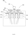
- Fig. 1A schematically shows an apparatus 400 that can carry out charged particle beam inspection using multiple beams of charge particles, where the charged particles in the multiple beams are from a single source (a multi-beam apparatus).
- the apparatus 400 has a source 401 that can produce charged particles in free space.
- the charged particles are electrons and the source 401 is an electron gun.
- the apparatus 400 has an optics system 419 that can generate with the charged particles multiple probe spots on a surface of a sample 407 and scan the probe spots on the surface of the sample 407.
- the optics system 419 may have a condenser lens 404 and a main aperture 405 upstream or downstream with respect to the condenser lens 404.
- the expression "Component A is upstream with respect to Component B” as used herein means that a beam of charged particles would reach Component A before reaching Component B in normal operation of the apparatus.
- the expression "Component B is downstream with respect to Component A” as used herein means that a beam of charged particles would reach Component B after reaching Component A in normal operation of the apparatus.
- the optics system 419 has a source-conversion unit 410 configured to form multiple virtual images (e.g., virtual images 402 and 403) of the source 401.
- the virtual images and the source 401 each can be viewed as an emitter of a beamlet (e.g., beamlets 431, 432 and 433).
- the source-conversion unit 410 may have an electrically conductive layer 412 with multiple openings that can divide the charged particles from the source 401 into multiple beamlets, and optics elements 411 that can influence the beamlets to form the virtual images of the source 401.
- the optics elements 411 may be micro-deflectors configured to deflect the beamlets.
- the electric current of the beamlets may be affected by the sizes of the openings in the electrically conductive layer 412 or the focusing power of the condenser lens 404.
- the optics system 419 includes an objective lens 406 configured to focus the multiple beamlets and thereby form multiple probe spots onto the surface of the sample 407.
- the source-conversion unit 410 may also have micro-compensators configured to reduce or eliminate aberrations (e.g., field curvature and astigmatism) of the probe spots.
- Fig. 1B schematically shows an alternative multi-beam apparatus.
- the condenser lens 404 collimates the charged particles from the source 401.
- the optics elements 411 of the source-conversion unit 410 may comprise micro-compensators 413.
- the micro-compensators 413 may be separate from micro-deflectors or may be integrated with micro-deflectors. If separated, the micro-compensators 413 may be positioned upstream to the micro-deflectors.
- the micro-compensators 413 are configured to compensate for off-axis aberrations (e.g., field curvature, astigmatism and distortion) of the condenser lens 404 or the objective lens 406.
- the off-axis aberrations may negatively impact the sizes or positions of the probe spots formed by off-axis (i.e., being not along the primary optical axis of the apparatus) beamlets.
- the off-axis aberrations of the objective lens 406 may not be completely eliminated by deflection of the beamlets.
- the micro-compensators 413 may compensate for the residue off-axis aberrations (i.e., the portion of the off-axis aberrations that cannot be eliminated by deflection of the beamlets) of the objective lens 406, or non-uniformity of the sizes of the probe spots.
- Each of the micro-compensators 413 is aligned with one of the openings in the electrically conductive layer 412.
- the micro-compensators 413 may each have four or more poles.
- the electric currents of the beamlets may be affected by the sizes of the openings in the electrically conductive layer 412 and/or the position of the condenser lens 404.
- Fig. 1C schematically shows an alternative multi-beam apparatus.
- the optics elements 411 of the source-conversion unit 410 may comprise pre-bending micro-deflectors 414.
- the pre-bending micro-deflectors 414 are micro-deflectors configured to bend the beamlets before they go through the openings in the electrically conductive layer 412.
- a source-conversion unit e.g., the source-conversion unit 410 in Fig. 1A , Fig. 1B or Fig. 1C
- the electric field caused by one optics element may extend into the beam path of another optics element and affect the beam transmitting through the other optics element.
- the micro-deflectors in the source-conversion unit 410 may bend the beamlets by electric fields and the electric field generated by one micro-deflector may extend into the beam path of a neighboring micro-deflector, thereby causing the beamlet through the neighboring micro-deflector to bend by an amount in addition to the bending caused by the electric field generated by the neighboring micro-deflector.
- the electric field (e.g., a quadrupole field or a round-lens field) generated by one of the micro-compensators in the source-conversion unit 410 may extend into the beam path of a neighboring micro-compensator, and thereby influencing the beamlet through the neighboring micro-compensator, by an amount in addition to the influence caused by the electric field generated by the neighboring micro-compensator.
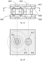
- Fig. 2A schematically shows crosstalk between two optics elements 611 and 612 integrated in a stack of wafers.
- Fig. 2B schematically shows a cross-sectional view along section A-A of Fig. 2A .
- the optics elements 611 and 612 are attached to an insulation layer 616.
- the optics elements 611 and 612 may have circular electrodes or multiple poles.
- an electric field is generated to influence (e.g., compensate for field curvature aberration of) a beamlet transmitting along a beam path 613 through the optics element 611.
- the equipotential lines 615 in Fig. 2A and Fig. 2B represent an electric field when the conductive plates 617 and 618 and the optics element 612 are at the same potential that is different from the potential of the optics element 611, the openings in the electrically conductive plates 617 and 618 are circular, and the optics elements 611 and 612 have circular electrodes.
- the electric field extends into a beam path 614 through the optics element 612.
- a beamlet passing through the optics element 612 thus may be affected not only by the electric field the optics element 612 generates but also by the electric field the optics element 611 generates, i.e., optics elements 611 and 612 have crosstalk.
- the equipotential lines 615 are not axisymmetric because the structure surrounding the optics element 611 is not axisymmetric.
- the electric field the optics element 611 generates comprises not only an axisymmetric component (also called a round-lens field), which compensates for the field curvature aberration, but also high order rotation-symmetric components such as a deflection field and a stigmator field.
- the high order components add aberrations to the beamlet passing through the optics element 611.
- Fig. 3A and Fig. 3B each schematically show a portion 700 of a source-conversion unit of a multi-beam apparatus, according to an embodiment.
- the portion 700 has multiple optics elements 710 (e.g., micro-deflectors, micro-lenses, micro-stigmators, micro-compensators) sandwiched between a first electrically conductive layer 720 and a second electrically conductive layer 740.
- the first electrically conductive layer 720 and the second electrically conductive layer 740 have openings that, collectively with the optics elements 710, form paths (e.g., paths 701, 702 and 703) of the beamlets.
- the portion 700 also has a third electrically conductive layer 730 with multiple holes that house the optics elements 710.
- the third electrically conductive layer 730 extends between the first electrically conductive layer 720 and the second electrically conductive layer 740.
- the third electrically conductive layer 730 is electrically connected to the first electrically conductive layer 720, or the second electrically conductive layer 740, or both.
- the third electrically conductive layer 730 is positioned between at least two of the optics elements 710, i.e., a plane the beam paths of the two optics elements 710 are on crosses the third electrically conductive layer 730.
- the walls among the holes of the third electrically conductive layer 730 can provide electrostatic shielding among the optics elements 710.
- the portion 700 has an electrically insulating layer 750.
- the electrically insulating layer 750 is physically connected to the optics elements 710.
- the electrically insulating layer 750 has discrete portions, each of which is physically connected to one of the optics elements 710.
- the electrically insulating layer 750 is physically connected to the first electrically conductive layer 720, the second electrically conductive layer 740, or the third electrically conductive layer 730.
- the electrically insulating layer 750 can provide mechanical support to the optics elements 710 and electrically insulate the optics elements 710 from the first electrically conductive layer 720, the second electrically conductive layer 740, and the third electrically conductive layer 730.
- the first electrically conductive layer 720, the second electrically conductive layer 740, and the third electrically conductive layer 730 collectively form cavities 760 electrically shielded from one another, where each of the cavities 760 accommodates one of the optics elements 710.
- the cavities 760 may have circular cross-sectional shape.
- the first electrically conductive layer 720, the second electrically conductive layer 740, and the third electrically conductive layer 730 may also be magnetically conductive to magnetically shield the beam paths from outside stray magnetic fields.
- the electrically insulating layer 750 is positioned upstream and downstream with respect to the optics elements 710, respectively.
- the third electrically conductive layer 730 is electrically connected to both the first electrically conductive layer 720 and the second electrically conductive layer 740.
- Fig. 3C and Fig. 3D each schematically show a portion 700 of a source-conversion unit of a multi-beam apparatus, according to an embodiment.
- the example shown in Fig. 3C is the same as the example in Fig. 3A , except that the electrically insulating layer 750 extends between the third electrically conductive layer 730 and the first electrically conductive layer 720.
- the electrically insulating layer 750 electrically insulates the first electrically conductive layer 720 from the optics elements 710.
- the electrically insulating layer 750 electrically may also insulate the first electrically conductive layer 720 from the third electrically conductive layer 730, and the second electrically conductive layer 740.
- the electrically insulating layer 750 may have one or more electrically conductive vias 723 through it and the conductive vias 723 electrically connect the first electrically conductive layer 720 to the third electrically conductive layer 730.
- the electrically insulating layer 750 can be very thin, such as less than 100 microns, less than 50 microns or less than 10 microns.
- the electrically insulating layer 750 can be an oxide, nitride or any other suitable material.
- the example shown in Fig. 3D is the same as the example in Fig. 3B , except that the electrically insulating layer 750 extends between the third electrically conductive layer 730 and the second electrically conductive layer 740.
- the electrically insulating layer 750 electrically insulates the second electrically conductive layer 740 from the optics elements 710.
- the electrically insulating layer 750 may also insulate the second electrically conductive layer 740 from the third electrically conductive layer 730 and the first electrically conductive layer 720.
- the electrically insulating layer 750 may have one or more electrically conductive vias 723 through it and thereby electrically connect the second electrically conductive layer 740 to the third electrically conductive layer 730 by the one or more electrically conductive vias 723 and the conductive vias 723 electrically connect the second electrically conductive layer 740 to the third electrically conductive layer 730.
- the electrically insulating layer 750 can be very thin, such as less than 100 microns, less than 50 microns or less than 10 microns.
- the electrically insulating layer 750 can be an oxide, nitride or any other suitable material.
- Fig. 3E and Fig. 3F each schematically show a portion 700 of a source-conversion unit of a multi-beam apparatus, according to an embodiment.
- the examples shown in Fig. 3E and Fig. 3F are the same as the examples in Fig. 3C and Fig. 3D , respectively, except that the electrically insulating layer 750 has an electrically conductive via 723 encircling each of the cavities 760 and the electrically conductive via 723 electrically connects the third electrically conductive layer 730 to the first electrically conductive layer 720 or the second electrically conductive layer 740.
- Fig. 3G schematically shows a cross-sectional view along section B-B of Fig. 3C or Fig. 3D .
- Fig. 3H schematically shows a portion 700 of a source-conversion unit of a multi-beam apparatus, according to an embodiment.
- the example shown in Fig. 3H is the same as the example in Fig. 3C , except that the portion 700 additional has a fourth electrically conductive layer 721 upstream to the first electrically conductive layer 720.
- the fourth electrically conductive layer 721 may be directly bonded to the first electrically conductive layer 720.
- the fourth electrically conductive layer 721 and the first electrically conductive layer 720 may have the same material.
- the fourth electrically conductive layer 721 has openings whose sidewall is thinned to reduce scattering of charged particles thereon. To thin the sidewall, the openings can have an inverted funnel or counterbore shape as shown in Fig. 3H .
- Fig. 3I schematically shows a portion 700 of a source-conversion unit of a multi-beam apparatus, according to an embodiment.
- the example shown in Fig. 3I is the same as the example in Fig. 3D , except that the portion 700 additional has a fifth electrically conductive layer 741 downstream to the second electrically conductive layer 740.
- the fifth electrically conductive layer 741 may be directly bonded to the second electrically conductive layer 740.
- the fifth electrically conductive layer 741 and the second electrically conductive layer 740 may have the same material.
- the fifth electrically conductive layer 741 has openings whose sidewall is thinned to reduce scattering of charged particles thereon. To thin the sidewall, the openings can have an inverted funnel or counterbore shape as shown in Fig. 3I .
- the materials suitable for the first electrically conductive layer 720, the third electrically conductive layer 730 and the second electrically conductive layer 740 may include semiconductors (e.g., silicon), and metals (e.g., gold).
- the first electrically conductive layer 720, the third electrically conductive layer 730 and the second electrically conductive layer 740 do not necessarily have the same materials.
- the first electrically conductive layer 720, the second electrically conductive layer 740, the third electrically conductive layer 730 can respectively be made from a semiconductor wafer, a semiconductor wafer with metal (e.g., gold) coating, or a dielectric plate with metal (e.g., gold) coating.
- the optics elements 710 can be made from a semiconductor wafer.
- the optics elements 710 and the third electrically conductive layer 730 can be made from a same semiconductor wafer, a same semiconductor wafer with metal (e.g., gold) coating, or a same dielectric plate with metal (e.g., gold) coating.
- the source-conversion unit shown in Fig. 3A-Fig. 3I can help reduce or eliminate crosstalk and field distribution deformation of the optics elements 710.
- a source-conversion unit may have portions 700 in Fig. 3A-Fig. 3I stacked on one another.
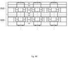
- Fig. 4A schematically shows a source-conversion unit including two of the portions 810 and 820 of Fig. 3C stacked on each other.
- the second electrically conductive layer 740 of the portion 810 upstream in the stack and the first electrically conductive layer 720 of the portion 820 downstream in the stack can be merged as a single layer.
- the optics elements 710 in the portion 810 may be micro-deflectors; the optics elements 710 in the portion 820 may be micro-compensators, which may comprise micro-lenses and micro-stigmators.
- the optics elements 710 along the same path may collectively serve as a micro-compensator.
- the openings in the second electrically conductive layer 740 of the portion 820 or the openings in the first electrically conductive layer 720 of the portion 810 may serve as the openings in the electrically conductive layer 412 in Fig. 1A , Fig. 1B or Fig. 1C .
- the sidewall of the openings may be thinned to reduce scattering of charged particles thereon. To thin the sidewall, the openings can have an inverted funnel or counterbore shape as shown in Fig. 4A .
- Fig. 4B shows another example of the source-conversion unit, which is similar to the source-conversion unit in Fig. 4A except that the portion 810 is the portion in Fig. 3H .
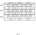
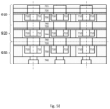
- Fig. 5A schematically shows a source-conversion unit including three of the portions 910, 920 and 930 of Fig. 3C stacked on one another.
- the second electrically conductive layer 740 of the portion 910 upstream in the stack and the first electrically conductive layer 720 of the portion 920 in the middle of the stack can be merged as a single layer; the second electrically conductive layer 740 of the portion 920 in the middle of the stack and the first electrically conductive layer 720 of the portion 930 downstream in the stack can be merged as a single layer.
- the optics elements 710 in the portions 910 and 920 may be micro-compensators, micro-lenses and micro-stigmators; the optics elements 710 in the portion 930 can be micro-deflectors.
- the openings in the first electrically conductive layer 720 of the portion 910 may serve as the openings in the electrically conductive layer 412 in Fig. 1B or Fig. 1C .
- the sidewall of the openings may be thinned to reduce scattering of charged particles thereon. To thin the sidewall, the openings can have an inverted funnel or counterbore shape as shown in Fig. 5A .
- Fig. 5B shows another example of the source-conversion unit, which is similar to the source-conversion unit in Fig. 5A except that the portion 910 is the portion in Fig. 3H .
- Fig. 6A schematically shows a source-conversion unit including three of the portions 910, 920 and 930 of Fig. 3D stacked on one another.
- the second electrically conductive layer 740 of the portion 910 upstream in the stack and the first electrically conductive layer 720 of the portion 920 in the middle of the stack can be merged as a single layer; the second electrically conductive layer 740 of the portion 920 in the middle of the stack and the first electrically conductive layer 720 of the portion 930 downstream in the stack can be merged as a single layer.
- the optics elements 710 in the portions 910 and 920 may be micro-compensators, micro-lenses and micro-stigmators; the optics elements 710 in the portion 930 can be micro-deflectors.
- the openings in the first electrically conductive layer 720 of the portion 910 may serve as the openings in the electrically conductive layer 412 in Fig. 1B or Fig. 1C .
- the sidewall of the openings may be thinned to reduce scattering of charged particles thereon. To thin the sidewall, the openings can have an inverted funnel or counterbore shape as shown in Fig. 6A .
- Fig. 6B shows another example of the source-conversion unit, which is similar to the source-conversion unit in Fig. 6A except that the portion 930 is the portion in Fig. 3I .
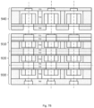
- Fig. 7A schematically shows a source-conversion unit including three of the portions 910, 920 and 930 of Fig. 3C stacked on one another (i.e., the structure of Fig. 5A ), and a portion 940 of Fig. 3D upstream to the stack of the portions 910, 920 and 930.
- the optics elements 710 in the portions 910 and 920 may be micro-compensators, micro-lenses and micro-stigmators; the optics elements 710 in the portion 930 can be micro-deflectors.
- the openings in the first electrically conductive layer 720 of the portion 910 may serve as the openings in the electrically conductive layer 412 in Fig. 1C .
- the sidewall of the openings may be thinned to reduce scattering of charged particles thereon.
- the openings can have an inverted funnel shape as shown in Fig. 6A .
- the optics elements 710 in the portion 940 may be pre-bending micro-deflectors.
- the sidewall of the openings in the first electrically conductive layer 720 of the portion 940 may be thinned to reduce scattering of charged particles thereon.
- the openings can have an inverted funnel or counterbore shape.
- Fig. 7B shows another example of the source-conversion unit, which is similar to the source-conversion unit in Fig. 7A except that the portion 910 is the portion in Fig. 3H .
- multi-beam apparatuses i.e., apparatuses that can carry out charged particle beam inspection using multiple beams of charge particles, where the charged particles in the multiple beams are from a single source
- the embodiments may be applicable in multi-column apparatuses (i.e., apparatuses that can carry out charged particle beam inspection using multiple beams of charge particles, where the multiple beams of charge particles are produced from multiple sources). Additional descriptions of multi-column apparatuses may be found in U.S. Patent 8,294,095 .
Landscapes
- Chemical & Material Sciences (AREA)
- Analytical Chemistry (AREA)
- Electron Beam Exposure (AREA)
- Testing Or Measuring Of Semiconductors Or The Like (AREA)
- Analysing Materials By The Use Of Radiation (AREA)
- Preparing Plates And Mask In Photomechanical Process (AREA)
- Exposure And Positioning Against Photoresist Photosensitive Materials (AREA)
Claims (14)
- Eine Vorrichtung, die Folgendes beinhaltet:eine erste elektrisch leitende Schicht (720);eine zweite elektrisch leitende Schicht (740);eine Vielzahl von Optikelementen (710) zwischen der ersten elektrisch leitenden Schicht (720) und der zweiten elektrisch leitenden Schicht (740), wobei die Vielzahl von Optikelementen (710) konfiguriert ist, um eine Vielzahl von Strahlen von Ladungsträgern zu beeinflussen;eine dritte elektrisch leitende Schicht (730) zwischen der ersten elektrisch leitenden Schicht (720) und der zweiten elektrisch leitenden Schicht (740); undeine elektrisch isolierende Schicht (750), die physisch mit den Optikelementen (710) verbunden ist, wobei die elektrisch isolierende Schicht (750) konfiguriert ist, um die Optikelemente (710) von der ersten elektrisch leitenden Schicht (720) und der zweiten elektrisch leitenden Schicht (740) elektrisch zu isolieren;wobei die Vorrichtung dadurch gekennzeichnet ist, dass die elektrisch isolierende Schicht (750) diskrete Abschnitte beinhaltet, von denen jeder physisch mit einem der Optikelemente (710) verbunden ist.
- Vorrichtung gemäß Anspruch 1, wobei die dritte elektrisch leitende Schicht (730) eine Vielzahl von Löchern beinhaltet, wobei die Löcher die Optikelemente (710) enthalten.
- Vorrichtung gemäß Anspruch 1, wobei die Optikelemente (710) von der dritten elektrisch leitenden Schicht (730) elektrisch isoliert sind.
- Vorrichtung gemäß Anspruch 1, wobei die dritte elektrisch leitende Schicht (730) mit der ersten elektrisch leitenden Schicht (720), der zweiten elektrisch leitenden Schicht (740) oder beiden elektrisch verbunden ist.
- Vorrichtung gemäß Anspruch 1, wobei die erste elektrisch leitende Schicht (720) und die zweite elektrisch leitende Schicht (740) Öffnungen beinhalten, wobei die Öffnungen und die Optikelemente (710) zusammen Wege (701, 702, 703) der Vielzahl von Strahlen von Ladungsträgern bilden.
- Vorrichtung gemäß Anspruch 5, wobei die Öffnungen die Form eines umgekehrten Trichters oder einer umgekehrten Senkbohrung aufweisen.
- Vorrichtung gemäß Anspruch 1, wobei die dritte elektrisch leitende Schicht (730) zwischen mindestens zwei der Optikelemente (710) positioniert ist.
- Vorrichtung gemäß Anspruch 1, wobei die erste elektrisch leitende Schicht (720), die zweite elektrisch leitende Schicht (740) und die dritte elektrisch leitende Schicht (730) zusammen Hohlräume (760) bilden, die die Optikelemente (710) fassen, wobei die Hohlräume (760) konfiguriert sind, um die Optikelemente (710) voneinander elektrisch abzuschirmen.
- Vorrichtung gemäß Anspruch 1, wobei die elektrisch isolierende Schicht (750) mit der ersten elektrisch leitenden Schicht (720), der zweiten elektrisch leitenden Schicht (740) oder der dritten elektrisch leitenden Schicht (730) physisch verbunden ist.
- Vorrichtung gemäß Anspruch 1, wobei die elektrisch isolierende Schicht (750) konfiguriert ist, um den Optikelementen (710) mechanische Stützung bereitzustellen.
- Vorrichtung gemäß Anspruch 1, wobei die elektrisch isolierende Schicht (750) in Bezug auf die Optikelemente (710) vorgelagert positioniert ist.
- Vorrichtung gemäß Anspruch 1, wobei die elektrisch isolierende Schicht (750) in Bezug auf die Optikelemente (710) nachgelagert positioniert ist.
- Vorrichtung gemäß Anspruch 1, wobei sich die elektrisch isolierende Schicht (750) zwischen der dritten elektrisch leitenden Schicht (730) und der ersten elektrisch leitenden Schicht (720) erstreckt und/oder wobei die elektrisch isolierende Schicht (750) die erste elektrisch leitende Schicht (720) von der dritten elektrisch leitenden Schicht (730), der zweiten elektrisch leitenden Schicht (740) und den Optikelementen (710) isoliert.
- Vorrichtung gemäß Anspruch 1, wobei sich die elektrisch isolierende Schicht (750) zwischen der dritten elektrisch leitenden Schicht (730) und der zweiten elektrisch leitenden Schicht (740) erstreckt.
Applications Claiming Priority (2)
| Application Number | Priority Date | Filing Date | Title |
|---|---|---|---|
| US201762492043P | 2017-04-28 | 2017-04-28 | |
| PCT/EP2018/058631 WO2018197169A1 (en) | 2017-04-28 | 2018-04-04 | An apparatus using multiple beams of charged particles |
Publications (2)
| Publication Number | Publication Date |
|---|---|
| EP3616231A1 EP3616231A1 (de) | 2020-03-04 |
| EP3616231B1 true EP3616231B1 (de) | 2024-03-06 |
Family
ID=61972507
Family Applications (1)
| Application Number | Title | Priority Date | Filing Date |
|---|---|---|---|
| EP18717874.4A Active EP3616231B1 (de) | 2017-04-28 | 2018-04-04 | Vorrichtung mit mehreren geladenen partikelstrahlen |
Country Status (8)
| Country | Link |
|---|---|
| US (4) | US11289304B2 (de) |
| EP (1) | EP3616231B1 (de) |
| JP (2) | JP6959989B2 (de) |
| KR (4) | KR102582001B1 (de) |
| CN (1) | CN110574139B (de) |
| IL (1) | IL270102B2 (de) |
| TW (3) | TWI746839B (de) |
| WO (1) | WO2018197169A1 (de) |
Families Citing this family (8)
| Publication number | Priority date | Publication date | Assignee | Title |
|---|---|---|---|---|
| EP3616231B1 (de) * | 2017-04-28 | 2024-03-06 | ASML Netherlands B.V. | Vorrichtung mit mehreren geladenen partikelstrahlen |
| WO2020141031A1 (en) * | 2018-12-31 | 2020-07-09 | Asml Netherlands B.V. | Multi-beam inspection apparatus |
| EP3948922A1 (de) | 2019-03-29 | 2022-02-09 | ASML Netherlands B.V. | Mehrstrahliges inspektionsgerät mit einstrahligem modus |
| IL287965B1 (en) * | 2019-05-31 | 2026-06-01 | Asml Netherlands Bv | Multiple charged particle beam device and methods of operating the same |
| JP7316106B2 (ja) * | 2019-06-14 | 2023-07-27 | 株式会社ニューフレアテクノロジー | 収差補正器及びマルチ電子ビーム照射装置 |
| JP7525387B2 (ja) * | 2020-12-15 | 2024-07-30 | 株式会社ニューフレアテクノロジー | 収差補正器 |
| DE102023126510B3 (de) | 2023-09-28 | 2025-02-13 | Carl Zeiss Multisem Gmbh | Monolithische Multi-Aperturplatte für ein Vielstrahl-Elektronenstrahlsystem, Verfahren zur Herstellung einer monolithischen Multi-Aperturplatte, und Vielstrahl-Elektronenstrahlsystem mit einer monolithischen Multi-Aperturplatte |
| US20260045437A1 (en) * | 2024-08-07 | 2026-02-12 | Kla Corporation | Field curvature corrector for use in multi-electron-beam optical system |
Family Cites Families (18)
| Publication number | Priority date | Publication date | Assignee | Title |
|---|---|---|---|---|
| US6175122B1 (en) * | 1998-01-09 | 2001-01-16 | International Business Machines Corporation | Method for writing a pattern using multiple variable shaped electron beams |
| JP2001284230A (ja) | 2000-03-31 | 2001-10-12 | Canon Inc | 電子光学系アレイ、これを用いた荷電粒子線露光装置ならびにデバイス製造方法 |
| EP1150327B1 (de) | 2000-04-27 | 2018-02-14 | ICT, Integrated Circuit Testing Gesellschaft für Halbleiterprüftechnik mbH | Mehrstrahl Ladungsträgerstrahlvorrichtung |
| EP2579268A1 (de) | 2003-09-05 | 2013-04-10 | Carl Zeiss SMT GmbH | Optische Partikelsysteme und Anordnungen und optische Partikelkomponenten für solche Systeme und Anordnungen |
| JP2008034498A (ja) | 2006-07-27 | 2008-02-14 | Canon Inc | 偏向器、露光装置、及びデバイス製造方法 |
| JP5491704B2 (ja) | 2007-05-14 | 2014-05-14 | イーエムエス ナノファブリカツィオン アーゲー | 対向電極アレイ板を有するパターン定義装置 |
| KR20120088780A (ko) | 2009-10-26 | 2012-08-08 | 마퍼 리쏘그라피 아이피 비.브이. | 변조 디바이스를 갖는 하전 입자 다중-빔렛 리소그라피 시스템 |
| US8294095B2 (en) | 2010-12-14 | 2012-10-23 | Hermes Microvision, Inc. | Apparatus of plural charged particle beams with multi-axis magnetic lens |
| NL2006868C2 (en) | 2011-05-30 | 2012-12-03 | Mapper Lithography Ip Bv | Charged particle multi-beamlet apparatus. |
| US9691588B2 (en) * | 2015-03-10 | 2017-06-27 | Hermes Microvision, Inc. | Apparatus of plural charged-particle beams |
| US10236156B2 (en) | 2015-03-25 | 2019-03-19 | Hermes Microvision Inc. | Apparatus of plural charged-particle beams |
| US9607805B2 (en) | 2015-05-12 | 2017-03-28 | Hermes Microvision Inc. | Apparatus of plural charged-particle beams |
| US9922799B2 (en) * | 2015-07-21 | 2018-03-20 | Hermes Microvision, Inc. | Apparatus of plural charged-particle beams |
| EP3809124A3 (de) | 2015-07-22 | 2022-03-16 | Hermes Microvision Inc. | Vorrichtung mit mehreren ladungsteilchenstrahlen |
| KR102068206B1 (ko) | 2015-11-30 | 2020-01-20 | 에이에스엠엘 네델란즈 비.브이. | 복수의 하전된 입자 빔의 장치 |
| US10062541B2 (en) | 2016-01-27 | 2018-08-28 | Hermes Microvision Inc. | Apparatus of plural charged-particle beams |
| IL267670B2 (en) | 2016-12-30 | 2025-10-01 | Asml Netherlands Bv | A device that uses multiple beams of charged particles |
| EP3616231B1 (de) * | 2017-04-28 | 2024-03-06 | ASML Netherlands B.V. | Vorrichtung mit mehreren geladenen partikelstrahlen |
-
2018
- 2018-04-04 EP EP18717874.4A patent/EP3616231B1/de active Active
- 2018-04-04 JP JP2019554971A patent/JP6959989B2/ja active Active
- 2018-04-04 KR KR1020227014093A patent/KR102582001B1/ko active Active
- 2018-04-04 KR KR1020257027443A patent/KR20250127345A/ko active Pending
- 2018-04-04 IL IL270102A patent/IL270102B2/en unknown
- 2018-04-04 WO PCT/EP2018/058631 patent/WO2018197169A1/en not_active Ceased
- 2018-04-04 KR KR1020197035121A patent/KR102392687B1/ko active Active
- 2018-04-04 KR KR1020237031893A patent/KR102848856B1/ko active Active
- 2018-04-04 US US16/608,741 patent/US11289304B2/en active Active
- 2018-04-04 CN CN201880027803.2A patent/CN110574139B/zh active Active
- 2018-04-26 TW TW107114123A patent/TWI746839B/zh active
- 2018-04-26 TW TW112117509A patent/TWI840220B/zh active
- 2018-04-26 TW TW110140104A patent/TWI814118B/zh active
-
2021
- 2021-10-08 JP JP2021165874A patent/JP7233503B2/ja active Active
-
2022
- 2022-03-28 US US17/656,731 patent/US11804356B2/en active Active
-
2023
- 2023-09-28 US US18/477,213 patent/US12237144B2/en active Active
-
2025
- 2025-01-16 US US19/025,881 patent/US20250157783A1/en active Pending
Also Published As
| Publication number | Publication date |
|---|---|
| TWI814118B (zh) | 2023-09-01 |
| KR102392687B1 (ko) | 2022-04-29 |
| CN110574139B (zh) | 2022-06-03 |
| US20240071711A1 (en) | 2024-02-29 |
| IL270102A (de) | 2019-12-31 |
| IL270102B2 (en) | 2024-08-01 |
| JP6959989B2 (ja) | 2021-11-05 |
| US12237144B2 (en) | 2025-02-25 |
| US20200203114A1 (en) | 2020-06-25 |
| TWI746839B (zh) | 2021-11-21 |
| KR20250127345A (ko) | 2025-08-26 |
| US20220223366A1 (en) | 2022-07-14 |
| KR20230136698A (ko) | 2023-09-26 |
| KR102848856B1 (ko) | 2025-08-21 |
| KR20200003064A (ko) | 2020-01-08 |
| EP3616231A1 (de) | 2020-03-04 |
| US11289304B2 (en) | 2022-03-29 |
| JP2020518092A (ja) | 2020-06-18 |
| KR20220058662A (ko) | 2022-05-09 |
| TWI840220B (zh) | 2024-04-21 |
| TW202232774A (zh) | 2022-08-16 |
| IL270102B1 (en) | 2024-04-01 |
| WO2018197169A1 (en) | 2018-11-01 |
| US20250157783A1 (en) | 2025-05-15 |
| US11804356B2 (en) | 2023-10-31 |
| JP2022002222A (ja) | 2022-01-06 |
| TW201907438A (zh) | 2019-02-16 |
| TW202401843A (zh) | 2024-01-01 |
| JP7233503B2 (ja) | 2023-03-06 |
| KR102582001B1 (ko) | 2023-09-22 |
| CN110574139A (zh) | 2019-12-13 |
Similar Documents
| Publication | Publication Date | Title |
|---|---|---|
| US12237144B2 (en) | Apparatus using multiple beams of charged particles | |
| US20230054632A1 (en) | Charged particle assessment tool, inspection method | |
| US20240044820A1 (en) | Methods of inspecting samples with a beam of charged particles | |
| US12087542B2 (en) | Image contrast enhancement in sample inspection | |
| US11430631B2 (en) | Methods of inspecting samples with multiple beams of charged particles | |
| JP2026510203A (ja) | 電子光学スタック、モジュール、評価装置、電子光学スタックを製造する方法 | |
| WO2024110486A1 (en) | Electron-optical element and method of assessing an electron-optical element |
Legal Events
| Date | Code | Title | Description |
|---|---|---|---|
| STAA | Information on the status of an ep patent application or granted ep patent |
Free format text: STATUS: UNKNOWN |
|
| STAA | Information on the status of an ep patent application or granted ep patent |
Free format text: STATUS: THE INTERNATIONAL PUBLICATION HAS BEEN MADE |
|
| PUAI | Public reference made under article 153(3) epc to a published international application that has entered the european phase |
Free format text: ORIGINAL CODE: 0009012 |
|
| STAA | Information on the status of an ep patent application or granted ep patent |
Free format text: STATUS: REQUEST FOR EXAMINATION WAS MADE |
|
| 17P | Request for examination filed |
Effective date: 20191021 |
|
| AK | Designated contracting states |
Kind code of ref document: A1 Designated state(s): AL AT BE BG CH CY CZ DE DK EE ES FI FR GB GR HR HU IE IS IT LI LT LU LV MC MK MT NL NO PL PT RO RS SE SI SK SM TR |
|
| AX | Request for extension of the european patent |
Extension state: BA ME |
|
| DAV | Request for validation of the european patent (deleted) | ||
| DAX | Request for extension of the european patent (deleted) | ||
| STAA | Information on the status of an ep patent application or granted ep patent |
Free format text: STATUS: EXAMINATION IS IN PROGRESS |
|
| 17Q | First examination report despatched |
Effective date: 20201120 |
|
| GRAP | Despatch of communication of intention to grant a patent |
Free format text: ORIGINAL CODE: EPIDOSNIGR1 |
|
| STAA | Information on the status of an ep patent application or granted ep patent |
Free format text: STATUS: GRANT OF PATENT IS INTENDED |
|
| INTG | Intention to grant announced |
Effective date: 20230503 |
|
| P01 | Opt-out of the competence of the unified patent court (upc) registered |
Effective date: 20230414 |
|
| GRAJ | Information related to disapproval of communication of intention to grant by the applicant or resumption of examination proceedings by the epo deleted |
Free format text: ORIGINAL CODE: EPIDOSDIGR1 |
|
| STAA | Information on the status of an ep patent application or granted ep patent |
Free format text: STATUS: EXAMINATION IS IN PROGRESS |
|
| INTC | Intention to grant announced (deleted) | ||
| GRAP | Despatch of communication of intention to grant a patent |
Free format text: ORIGINAL CODE: EPIDOSNIGR1 |
|
| STAA | Information on the status of an ep patent application or granted ep patent |
Free format text: STATUS: GRANT OF PATENT IS INTENDED |
|
| INTG | Intention to grant announced |
Effective date: 20231127 |
|
| GRAS | Grant fee paid |
Free format text: ORIGINAL CODE: EPIDOSNIGR3 |
|
| GRAA | (expected) grant |
Free format text: ORIGINAL CODE: 0009210 |
|
| STAA | Information on the status of an ep patent application or granted ep patent |
Free format text: STATUS: THE PATENT HAS BEEN GRANTED |
|
| AK | Designated contracting states |
Kind code of ref document: B1 Designated state(s): AL AT BE BG CH CY CZ DE DK EE ES FI FR GB GR HR HU IE IS IT LI LT LU LV MC MK MT NL NO PL PT RO RS SE SI SK SM TR |
|
| REG | Reference to a national code |
Ref country code: GB Ref legal event code: FG4D |
|
| REG | Reference to a national code |
Ref country code: CH Ref legal event code: EP |
|
| REG | Reference to a national code |
Ref country code: DE Ref legal event code: R096 Ref document number: 602018066173 Country of ref document: DE |
|
| REG | Reference to a national code |
Ref country code: IE Ref legal event code: FG4D |
|
| REG | Reference to a national code |
Ref country code: LT Ref legal event code: MG9D |
|
| PG25 | Lapsed in a contracting state [announced via postgrant information from national office to epo] |
Ref country code: LT Free format text: LAPSE BECAUSE OF FAILURE TO SUBMIT A TRANSLATION OF THE DESCRIPTION OR TO PAY THE FEE WITHIN THE PRESCRIBED TIME-LIMIT Effective date: 20240306 |
|
| REG | Reference to a national code |
Ref country code: NL Ref legal event code: MP Effective date: 20240306 |
|
| PG25 | Lapsed in a contracting state [announced via postgrant information from national office to epo] |
Ref country code: GR Free format text: LAPSE BECAUSE OF FAILURE TO SUBMIT A TRANSLATION OF THE DESCRIPTION OR TO PAY THE FEE WITHIN THE PRESCRIBED TIME-LIMIT Effective date: 20240607 |
|
| PG25 | Lapsed in a contracting state [announced via postgrant information from national office to epo] |
Ref country code: RS Free format text: LAPSE BECAUSE OF FAILURE TO SUBMIT A TRANSLATION OF THE DESCRIPTION OR TO PAY THE FEE WITHIN THE PRESCRIBED TIME-LIMIT Effective date: 20240606 Ref country code: HR Free format text: LAPSE BECAUSE OF FAILURE TO SUBMIT A TRANSLATION OF THE DESCRIPTION OR TO PAY THE FEE WITHIN THE PRESCRIBED TIME-LIMIT Effective date: 20240306 |
|
| PG25 | Lapsed in a contracting state [announced via postgrant information from national office to epo] |
Ref country code: ES Free format text: LAPSE BECAUSE OF FAILURE TO SUBMIT A TRANSLATION OF THE DESCRIPTION OR TO PAY THE FEE WITHIN THE PRESCRIBED TIME-LIMIT Effective date: 20240306 |
|
| PG25 | Lapsed in a contracting state [announced via postgrant information from national office to epo] |
Ref country code: RS Free format text: LAPSE BECAUSE OF FAILURE TO SUBMIT A TRANSLATION OF THE DESCRIPTION OR TO PAY THE FEE WITHIN THE PRESCRIBED TIME-LIMIT Effective date: 20240606 Ref country code: NO Free format text: LAPSE BECAUSE OF FAILURE TO SUBMIT A TRANSLATION OF THE DESCRIPTION OR TO PAY THE FEE WITHIN THE PRESCRIBED TIME-LIMIT Effective date: 20240606 Ref country code: LT Free format text: LAPSE BECAUSE OF FAILURE TO SUBMIT A TRANSLATION OF THE DESCRIPTION OR TO PAY THE FEE WITHIN THE PRESCRIBED TIME-LIMIT Effective date: 20240306 Ref country code: HR Free format text: LAPSE BECAUSE OF FAILURE TO SUBMIT A TRANSLATION OF THE DESCRIPTION OR TO PAY THE FEE WITHIN THE PRESCRIBED TIME-LIMIT Effective date: 20240306 Ref country code: GR Free format text: LAPSE BECAUSE OF FAILURE TO SUBMIT A TRANSLATION OF THE DESCRIPTION OR TO PAY THE FEE WITHIN THE PRESCRIBED TIME-LIMIT Effective date: 20240607 Ref country code: FI Free format text: LAPSE BECAUSE OF FAILURE TO SUBMIT A TRANSLATION OF THE DESCRIPTION OR TO PAY THE FEE WITHIN THE PRESCRIBED TIME-LIMIT Effective date: 20240306 Ref country code: ES Free format text: LAPSE BECAUSE OF FAILURE TO SUBMIT A TRANSLATION OF THE DESCRIPTION OR TO PAY THE FEE WITHIN THE PRESCRIBED TIME-LIMIT Effective date: 20240306 Ref country code: BG Free format text: LAPSE BECAUSE OF FAILURE TO SUBMIT A TRANSLATION OF THE DESCRIPTION OR TO PAY THE FEE WITHIN THE PRESCRIBED TIME-LIMIT Effective date: 20240306 |
|
| REG | Reference to a national code |
Ref country code: AT Ref legal event code: MK05 Ref document number: 1664400 Country of ref document: AT Kind code of ref document: T Effective date: 20240306 |
|
| PG25 | Lapsed in a contracting state [announced via postgrant information from national office to epo] |
Ref country code: SE Free format text: LAPSE BECAUSE OF FAILURE TO SUBMIT A TRANSLATION OF THE DESCRIPTION OR TO PAY THE FEE WITHIN THE PRESCRIBED TIME-LIMIT Effective date: 20240306 Ref country code: LV Free format text: LAPSE BECAUSE OF FAILURE TO SUBMIT A TRANSLATION OF THE DESCRIPTION OR TO PAY THE FEE WITHIN THE PRESCRIBED TIME-LIMIT Effective date: 20240306 |
|
| PG25 | Lapsed in a contracting state [announced via postgrant information from national office to epo] |
Ref country code: NL Free format text: LAPSE BECAUSE OF FAILURE TO SUBMIT A TRANSLATION OF THE DESCRIPTION OR TO PAY THE FEE WITHIN THE PRESCRIBED TIME-LIMIT Effective date: 20240306 |
|
| PG25 | Lapsed in a contracting state [announced via postgrant information from national office to epo] |
Ref country code: NL Free format text: LAPSE BECAUSE OF FAILURE TO SUBMIT A TRANSLATION OF THE DESCRIPTION OR TO PAY THE FEE WITHIN THE PRESCRIBED TIME-LIMIT Effective date: 20240306 |
|
| PG25 | Lapsed in a contracting state [announced via postgrant information from national office to epo] |
Ref country code: IS Free format text: LAPSE BECAUSE OF FAILURE TO SUBMIT A TRANSLATION OF THE DESCRIPTION OR TO PAY THE FEE WITHIN THE PRESCRIBED TIME-LIMIT Effective date: 20240706 |
|
| PG25 | Lapsed in a contracting state [announced via postgrant information from national office to epo] |
Ref country code: SM Free format text: LAPSE BECAUSE OF FAILURE TO SUBMIT A TRANSLATION OF THE DESCRIPTION OR TO PAY THE FEE WITHIN THE PRESCRIBED TIME-LIMIT Effective date: 20240306 Ref country code: PT Free format text: LAPSE BECAUSE OF FAILURE TO SUBMIT A TRANSLATION OF THE DESCRIPTION OR TO PAY THE FEE WITHIN THE PRESCRIBED TIME-LIMIT Effective date: 20240708 |
|
| PG25 | Lapsed in a contracting state [announced via postgrant information from national office to epo] |
Ref country code: CZ Free format text: LAPSE BECAUSE OF FAILURE TO SUBMIT A TRANSLATION OF THE DESCRIPTION OR TO PAY THE FEE WITHIN THE PRESCRIBED TIME-LIMIT Effective date: 20240306 Ref country code: EE Free format text: LAPSE BECAUSE OF FAILURE TO SUBMIT A TRANSLATION OF THE DESCRIPTION OR TO PAY THE FEE WITHIN THE PRESCRIBED TIME-LIMIT Effective date: 20240306 |
|
| PG25 | Lapsed in a contracting state [announced via postgrant information from national office to epo] |
Ref country code: AT Free format text: LAPSE BECAUSE OF FAILURE TO SUBMIT A TRANSLATION OF THE DESCRIPTION OR TO PAY THE FEE WITHIN THE PRESCRIBED TIME-LIMIT Effective date: 20240306 |
|
| PG25 | Lapsed in a contracting state [announced via postgrant information from national office to epo] |
Ref country code: PL Free format text: LAPSE BECAUSE OF FAILURE TO SUBMIT A TRANSLATION OF THE DESCRIPTION OR TO PAY THE FEE WITHIN THE PRESCRIBED TIME-LIMIT Effective date: 20240306 |
|
| PG25 | Lapsed in a contracting state [announced via postgrant information from national office to epo] |
Ref country code: SK Free format text: LAPSE BECAUSE OF FAILURE TO SUBMIT A TRANSLATION OF THE DESCRIPTION OR TO PAY THE FEE WITHIN THE PRESCRIBED TIME-LIMIT Effective date: 20240306 |
|
| PG25 | Lapsed in a contracting state [announced via postgrant information from national office to epo] |
Ref country code: SM Free format text: LAPSE BECAUSE OF FAILURE TO SUBMIT A TRANSLATION OF THE DESCRIPTION OR TO PAY THE FEE WITHIN THE PRESCRIBED TIME-LIMIT Effective date: 20240306 Ref country code: SK Free format text: LAPSE BECAUSE OF FAILURE TO SUBMIT A TRANSLATION OF THE DESCRIPTION OR TO PAY THE FEE WITHIN THE PRESCRIBED TIME-LIMIT Effective date: 20240306 Ref country code: RO Free format text: LAPSE BECAUSE OF FAILURE TO SUBMIT A TRANSLATION OF THE DESCRIPTION OR TO PAY THE FEE WITHIN THE PRESCRIBED TIME-LIMIT Effective date: 20240306 Ref country code: PT Free format text: LAPSE BECAUSE OF FAILURE TO SUBMIT A TRANSLATION OF THE DESCRIPTION OR TO PAY THE FEE WITHIN THE PRESCRIBED TIME-LIMIT Effective date: 20240708 Ref country code: PL Free format text: LAPSE BECAUSE OF FAILURE TO SUBMIT A TRANSLATION OF THE DESCRIPTION OR TO PAY THE FEE WITHIN THE PRESCRIBED TIME-LIMIT Effective date: 20240306 Ref country code: IS Free format text: LAPSE BECAUSE OF FAILURE TO SUBMIT A TRANSLATION OF THE DESCRIPTION OR TO PAY THE FEE WITHIN THE PRESCRIBED TIME-LIMIT Effective date: 20240706 Ref country code: EE Free format text: LAPSE BECAUSE OF FAILURE TO SUBMIT A TRANSLATION OF THE DESCRIPTION OR TO PAY THE FEE WITHIN THE PRESCRIBED TIME-LIMIT Effective date: 20240306 Ref country code: CZ Free format text: LAPSE BECAUSE OF FAILURE TO SUBMIT A TRANSLATION OF THE DESCRIPTION OR TO PAY THE FEE WITHIN THE PRESCRIBED TIME-LIMIT Effective date: 20240306 Ref country code: AT Free format text: LAPSE BECAUSE OF FAILURE TO SUBMIT A TRANSLATION OF THE DESCRIPTION OR TO PAY THE FEE WITHIN THE PRESCRIBED TIME-LIMIT Effective date: 20240306 |
|
| REG | Reference to a national code |
Ref country code: CH Ref legal event code: PL |
|
| PG25 | Lapsed in a contracting state [announced via postgrant information from national office to epo] |
Ref country code: IT Free format text: LAPSE BECAUSE OF FAILURE TO SUBMIT A TRANSLATION OF THE DESCRIPTION OR TO PAY THE FEE WITHIN THE PRESCRIBED TIME-LIMIT Effective date: 20240306 |
|
| REG | Reference to a national code |
Ref country code: DE Ref legal event code: R097 Ref document number: 602018066173 Country of ref document: DE |
|
| PG25 | Lapsed in a contracting state [announced via postgrant information from national office to epo] |
Ref country code: LU Free format text: LAPSE BECAUSE OF NON-PAYMENT OF DUE FEES Effective date: 20240404 |
|
| REG | Reference to a national code |
Ref country code: BE Ref legal event code: MM Effective date: 20240430 |
|
| PG25 | Lapsed in a contracting state [announced via postgrant information from national office to epo] |
Ref country code: LU Free format text: LAPSE BECAUSE OF NON-PAYMENT OF DUE FEES Effective date: 20240404 Ref country code: IT Free format text: LAPSE BECAUSE OF FAILURE TO SUBMIT A TRANSLATION OF THE DESCRIPTION OR TO PAY THE FEE WITHIN THE PRESCRIBED TIME-LIMIT Effective date: 20240306 |
|
| PG25 | Lapsed in a contracting state [announced via postgrant information from national office to epo] |
Ref country code: MC Free format text: LAPSE BECAUSE OF FAILURE TO SUBMIT A TRANSLATION OF THE DESCRIPTION OR TO PAY THE FEE WITHIN THE PRESCRIBED TIME-LIMIT Effective date: 20240306 |
|
| PLBE | No opposition filed within time limit |
Free format text: ORIGINAL CODE: 0009261 |
|
| STAA | Information on the status of an ep patent application or granted ep patent |
Free format text: STATUS: NO OPPOSITION FILED WITHIN TIME LIMIT |
|
| PG25 | Lapsed in a contracting state [announced via postgrant information from national office to epo] |
Ref country code: DK Free format text: LAPSE BECAUSE OF FAILURE TO SUBMIT A TRANSLATION OF THE DESCRIPTION OR TO PAY THE FEE WITHIN THE PRESCRIBED TIME-LIMIT Effective date: 20240306 |
|
| PG25 | Lapsed in a contracting state [announced via postgrant information from national office to epo] |
Ref country code: BE Free format text: LAPSE BECAUSE OF NON-PAYMENT OF DUE FEES Effective date: 20240430 |
|
| PG25 | Lapsed in a contracting state [announced via postgrant information from national office to epo] |
Ref country code: MC Free format text: LAPSE BECAUSE OF FAILURE TO SUBMIT A TRANSLATION OF THE DESCRIPTION OR TO PAY THE FEE WITHIN THE PRESCRIBED TIME-LIMIT Effective date: 20240306 Ref country code: DK Free format text: LAPSE BECAUSE OF FAILURE TO SUBMIT A TRANSLATION OF THE DESCRIPTION OR TO PAY THE FEE WITHIN THE PRESCRIBED TIME-LIMIT Effective date: 20240306 Ref country code: BE Free format text: LAPSE BECAUSE OF NON-PAYMENT OF DUE FEES Effective date: 20240430 Ref country code: CH Free format text: LAPSE BECAUSE OF NON-PAYMENT OF DUE FEES Effective date: 20240430 |
|
| 26N | No opposition filed |
Effective date: 20241209 |
|
| GBPC | Gb: european patent ceased through non-payment of renewal fee |
Effective date: 20240606 |
|
| PG25 | Lapsed in a contracting state [announced via postgrant information from national office to epo] |
Ref country code: SI Free format text: LAPSE BECAUSE OF FAILURE TO SUBMIT A TRANSLATION OF THE DESCRIPTION OR TO PAY THE FEE WITHIN THE PRESCRIBED TIME-LIMIT Effective date: 20240306 |
|
| PG25 | Lapsed in a contracting state [announced via postgrant information from national office to epo] |
Ref country code: FR Free format text: LAPSE BECAUSE OF NON-PAYMENT OF DUE FEES Effective date: 20240506 |
|
| PG25 | Lapsed in a contracting state [announced via postgrant information from national office to epo] |
Ref country code: GB Free format text: LAPSE BECAUSE OF NON-PAYMENT OF DUE FEES Effective date: 20240606 |
|
| PG25 | Lapsed in a contracting state [announced via postgrant information from national office to epo] |
Ref country code: CY Free format text: LAPSE BECAUSE OF FAILURE TO SUBMIT A TRANSLATION OF THE DESCRIPTION OR TO PAY THE FEE WITHIN THE PRESCRIBED TIME-LIMIT; INVALID AB INITIO Effective date: 20180404 |
|
| PG25 | Lapsed in a contracting state [announced via postgrant information from national office to epo] |
Ref country code: HU Free format text: LAPSE BECAUSE OF FAILURE TO SUBMIT A TRANSLATION OF THE DESCRIPTION OR TO PAY THE FEE WITHIN THE PRESCRIBED TIME-LIMIT; INVALID AB INITIO Effective date: 20180404 |
|
| PG25 | Lapsed in a contracting state [announced via postgrant information from national office to epo] |
Ref country code: TR Free format text: LAPSE BECAUSE OF FAILURE TO SUBMIT A TRANSLATION OF THE DESCRIPTION OR TO PAY THE FEE WITHIN THE PRESCRIBED TIME-LIMIT Effective date: 20240306 |
|
| PGFP | Annual fee paid to national office [announced via postgrant information from national office to epo] |
Ref country code: DE Payment date: 20260421 Year of fee payment: 9 |
|
| PGFP | Annual fee paid to national office [announced via postgrant information from national office to epo] |
Ref country code: IE Payment date: 20260423 Year of fee payment: 9 |