EP3614438A1 - Organic electroluminescent device, display and mobile communication apparatus - Google Patents
Organic electroluminescent device, display and mobile communication apparatus Download PDFInfo
- Publication number
- EP3614438A1 EP3614438A1 EP18872604.6A EP18872604A EP3614438A1 EP 3614438 A1 EP3614438 A1 EP 3614438A1 EP 18872604 A EP18872604 A EP 18872604A EP 3614438 A1 EP3614438 A1 EP 3614438A1
- Authority
- EP
- European Patent Office
- Prior art keywords
- pixel definition
- electrode
- organic electroluminescent
- blocks
- electroluminescent device
- Prior art date
- Legal status (The legal status is an assumption and is not a legal conclusion. Google has not performed a legal analysis and makes no representation as to the accuracy of the status listed.)
- Ceased
Links
Images

Classifications
-
- H—ELECTRICITY
- H10—SEMICONDUCTOR DEVICES; ELECTRIC SOLID-STATE DEVICES NOT OTHERWISE PROVIDED FOR
- H10K—ORGANIC ELECTRIC SOLID-STATE DEVICES
- H10K59/00—Integrated devices, or assemblies of multiple devices, comprising at least one organic light-emitting element covered by group H10K50/00
- H10K59/10—OLED displays
- H10K59/12—Active-matrix OLED [AMOLED] displays
- H10K59/122—Pixel-defining structures or layers, e.g. banks
-
- H—ELECTRICITY
- H10—SEMICONDUCTOR DEVICES; ELECTRIC SOLID-STATE DEVICES NOT OTHERWISE PROVIDED FOR
- H10K—ORGANIC ELECTRIC SOLID-STATE DEVICES
- H10K50/00—Organic light-emitting devices
- H10K50/80—Constructional details
- H10K50/805—Electrodes
-
- H—ELECTRICITY
- H10—SEMICONDUCTOR DEVICES; ELECTRIC SOLID-STATE DEVICES NOT OTHERWISE PROVIDED FOR
- H10K—ORGANIC ELECTRIC SOLID-STATE DEVICES
- H10K59/00—Integrated devices, or assemblies of multiple devices, comprising at least one organic light-emitting element covered by group H10K50/00
- H10K59/10—OLED displays
- H10K59/12—Active-matrix OLED [AMOLED] displays
- H10K59/131—Interconnections, e.g. wiring lines or terminals
-
- H—ELECTRICITY
- H10—SEMICONDUCTOR DEVICES; ELECTRIC SOLID-STATE DEVICES NOT OTHERWISE PROVIDED FOR
- H10K—ORGANIC ELECTRIC SOLID-STATE DEVICES
- H10K59/00—Integrated devices, or assemblies of multiple devices, comprising at least one organic light-emitting element covered by group H10K50/00
- H10K59/10—OLED displays
- H10K59/17—Passive-matrix OLED displays
- H10K59/173—Passive-matrix OLED displays comprising banks or shadow masks
-
- H—ELECTRICITY
- H10—SEMICONDUCTOR DEVICES; ELECTRIC SOLID-STATE DEVICES NOT OTHERWISE PROVIDED FOR
- H10K—ORGANIC ELECTRIC SOLID-STATE DEVICES
- H10K71/00—Manufacture or treatment specially adapted for the organic devices covered by this subclass
- H10K71/50—Forming devices by joining two substrates together, e.g. lamination techniques
-
- H—ELECTRICITY
- H10—SEMICONDUCTOR DEVICES; ELECTRIC SOLID-STATE DEVICES NOT OTHERWISE PROVIDED FOR
- H10K—ORGANIC ELECTRIC SOLID-STATE DEVICES
- H10K2102/00—Constructional details relating to the organic devices covered by this subclass
- H10K2102/301—Details of OLEDs
- H10K2102/302—Details of OLEDs of OLED structures
Definitions
- the application relates to a field of an organic electroluminescent device, and in particular to an improvement of a layout of an overlapped area of an organic electroluminescent device.
- an Organic Light Emitting Diode (OLED for short), as a current-type light-emitting device, is increasingly used in a field of high-performance display for its characteristics such as self-luminance, fast response, wide viewing angle, fabrication on a flexible substrate.
- a technical problem to be solved by the application is insufficient aperture ratio of the organic electroluminescent device in a cathode overlapped area, resulting in uneven brightness of the screen body.
- the application provides an organic electroluminescent device, a display and a mobile communication apparatus applied thereto.
- An organic electroluminescent device having an overlapped area located at an edge of a non-display area comprising:
- vertical projection positions of the plurality of supporting blocks of the isolation layer are the same as vertical projection positions of the plurality of the pixel definition blocks of the pixel definition layer.
- an area of any one of the plurality of pixel definition blocks is larger than an area of a corresponding supporting block thereof.
- the first electrode of the organic electroluminescent device of the application further comprises, in the overlapped area, a plurality of openings which are arranged in the same manner as the plurality of pixel definition blocks of the pixel definition layer.
- vertical projection positions of the plurality of openings of the first electrode are the same as vertical projection positions of the plurality of pixel definition blocks of the pixel definition layer.
- the plurality of pixel definition blocks of the plurality of pixel definition layer fill in and cover the plurality of openings of the first electrode.
- the first electrode and the second electrode are transparent electrodes.
- the plurality of pixel definition blocks and the plurality of supporting blocks are both made from organic materials.
- the application also includes an organic electroluminescent display comprising a flexible printed circuit board (FPC) and a power supply interface, and the organic electroluminescent display uses the above-mentioned organic electroluminescent device.
- an organic electroluminescent display comprising a flexible printed circuit board (FPC) and a power supply interface
- the organic electroluminescent display uses the above-mentioned organic electroluminescent device.
- the application also includes a mobile communication apparatus comprising a communication device and a display device, the display device being the above-mentioned organic electroluminescent display.
- the organic electroluminescent device of the application via the same arrangement manner or the same vertical projection position for the supporting blocks and the pixel definition blocks, can reduce shielding of the cathode overlapped area, increase a aperture ratio of the cathode overlapped area, and reduce a voltage drop of Vss wires, thereby improving a problem of uneven brightness of a screen body.
- the organic electroluminescent device of the application via the same arrangement manner or the same vertical projection position for the supporting blocks and the openings, can reduce the shielding of the cathode overlapped area, increase the aperture ratio of the cathode overlapped area, and reduce the voltage drop of the Vss wires, thereby improving the problem of uneven brightness of the screen body.
- the organic electroluminescent device of the application enables, via a stack manner in the application, a thickness from a bottom end of a substrate to the supporting block is the same or close whether in the overlapped area or in the display area, which is advantageous for enhancing an impact resistance ability of the screen body of the organic electroluminescence device.
- FIG. 1 is a schematic structural view of an organic electroluminescent device according to an embodiment of the application.
- a substrate 1 includes a display area 11 and a non-display area 12.
- the display area 11 is arranged on the substrate 10, and the non-display area 12 is arranged in an area on the substrate 10 outside the display area 11.
- the non-display area 12 also includes an overlapped area 121 and a drive circuit area 122.
- the overlapped area 121 is located at the edge of the non-display area 12, and the drive circuit area 122 is located between the overlapped area 121 and the display area 11.
- the overlapped area 121 is a cathode overlapped area, but the application is not limited thereto.
- FIG. 2 is a cross-sectional view taken along a line A-A' of the structure of the organic electroluminescent device according to an embodiment of the application;
- the cross-sectional view taken along the line A-A' shown in Fig. 2 is a cross-sectional view of the overlapped area 121 of the non-display area 12 of Fig. 1 .
- the overlapped area 121 of the organic electroluminescent device of the application further includes a planarizing layer 2, a pixel definition layer, a first electrode 41, a second electrode 42, and an isolation layer.
- the planarizing layer 2 is arranged on the substrate 1, and the first electrode 41 is arranged on the planarizing layer 2 of the overlapped area.
- the pixel definition layer is arranged on the first electrode 41, and further includes a plurality of pixel definition blocks 3.
- the isolation layer is arranged on the pixel definition layer, and the isolation layer further includes a plurality of supporting blocks 5.
- the second electrode 42 covers the first electrode 41, the plurality of pixel definition blocks 3, and the plurality of supporting blocks 5 in the overlapped area 121.
- the second electrode 42 overlaps the first electrode 41.
- the first electrode 41 may be an anode layer in an organic electroluminescent device during a manufacturing process
- the second electrode 42 may be a cathode layer in the organic electroluminescent device during the manufacturing process.
- the second electrode 42 is connected to the first electrode 41 by the way of overlaying (also called overlapped).
- the first electrode 41 and the second electrode 42 are transparent electrodes, and the second electrode 42 may also have an integrated structure.
- the plurality of pixel definition blocks 3 and the plurality of supporting blocks 5 may both be made from organic materials, but the application is not limited thereto.
- the arrangement manner of the plurality of supporting blocks 5 of the isolation layer are the same as the arrangement manner of the plurality of the pixel definition blocks 3 of the pixel definition layer.
- the vertical projection positions of the plurality of supporting blocks 5 of the isolation layer are the same as the vertical projection positions of the plurality of pixel definition blocks 3 of the pixel definition layer.
- the area of the plurality of pixel definition blocks 3 of the pixel definition layer may be larger than that of the plurality of supporting blocks 5 of the isolation layer, but the application is not limited thereto.
- the first electrode 41 further includes a plurality of openings 410 in the overlapped area 121.
- the plurality of openings 410 may be cylindrical, square cylindrical or tapered, but the application is not limited thereto.
- the arrangement manner of the plurality of openings 410 is the same as the arrangement manner of the plurality of pixel definition blocks 3 of the pixel definition layer.
- the vertical projection positions of the plurality of openings 410 of the first electrode 41 are the same as the vertical projection positions of the plurality of pixel definition blocks 3 of the pixel definition layer.
- the pixel definition block 3 of the pixel definition layer may further fill in and cover a plurality of openings 410 of the first electrode 41.
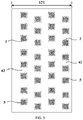
- FIG. 3 is an enlarged schematic view showing an overlapped area of the structure of the organic electroluminescent device according to an embodiment of the application.
- a partial enlarged view shown in FIG. 3 is a schematic layout top view of an M area in the overlapped area 121 of the non-display area of FIG.1 .
- a plurality of supporting blocks 5 overlap with the pixel definition blocks 3, and in the layout top view, a plurality of openings 410 not shown actually overlap with a plurality of pixel definition blocks 3 of the pixel definition layer. It can be understood with reference to the cross-sectional view of FIG.
- the vertical projection positions of the plurality of pixel definition blocks 3 of the pixel definition layer are the same as the vertical projection positions of the plurality of openings 410 of the first electrode 41, and the vertical projection positions of the plurality of supporting blocks 5 of the isolation layer are further the same as the vertical projection position of the plurality of pixel definition blocks 3 of the pixel definition layer, thus it can be understood that the vertical projection positions of the pixel definition blocks 3, the openings 410, and the supporting blocks 5 can all be the same.
- the plurality of supporting blocks 5 and the plurality of pixel definition blocks 3 are arranged with a spacing, and the spacing distance may be equidistant, equidifferently increased, or equidifferently decreased.
- the arrangement manner of the plurality of supporting blocks 5 of the isolation layer is the same as the arrangement manner of the plurality of pixel definition blocks 3 of the pixel definition layer.
- An area of the pixel definition blocks 3 may be greater than or equal to an area of the supporting blocks 5, and can be adaptively adjusted according to actual design requirements. In the illustration of the embodiment, the area of the pixel definition block 3 is larger than the area of the supporting block 5, however, the application is not limited thereto.
- the arrangement manner of the pixel definition blocks 3 and the supporting blocks 5 in the overlapped area 121 is the same manner as the arrangement manner of the pixel definition blocks 3 and the supporting blocks 5 in the display area 11.
- the organic electroluminescent device of the application enables, via the stack manner in the application, a thickness from a bottom end of the substrate 1 to the supporting block 5 is the same or close whether in the overlapped area 121 or in the display area 11, which is advantageous for enhancing the impact resistance ability of the screen body of the organic electroluminescence device.
- the organic electroluminescent device can perform the quality test on impact resistance of the screen body through a drop ball test for quality inspection.
- the pass rate of the drop ball test of the organic electroluminescent device in the embodiment of the application is significantly higher than that in the prior art, which is sufficient to confirm that the organic electroluminescent device of the embodiment of the application can effectively improve the impact resistance of the screen body.
- the organic electroluminescent device of the application via the same arrangement manner or the same vertical projection position of the pixel definition blocks 3, the supporting blocks 5 and the openings 410, can reduce the shielding of the cathode overlapped area, increase the aperture ratio of the cathode overlapped area, and reduce the voltage drop of the Vss wires, thereby improving the problem of uneven brightness of the screen body.
- the application further proposes an organic electroluminescent display which uses the aforementioned organic electroluminescent device, including a flexible printed circuit board (FPC) and a power supply interface.
- a mobile communication apparatus including a communication device and a display device which is the aforementioned organic electroluminescence display.
Landscapes
- Engineering & Computer Science (AREA)
- Microelectronics & Electronic Packaging (AREA)
- Physics & Mathematics (AREA)
- Optics & Photonics (AREA)
- Manufacturing & Machinery (AREA)
- Electroluminescent Light Sources (AREA)
- Devices For Indicating Variable Information By Combining Individual Elements (AREA)
Abstract
Description
- The present application claims priority to Chinese Patent Application No.
201711053191.8, filed on October 31, 2017 - The application relates to a field of an organic electroluminescent device, and in particular to an improvement of a layout of an overlapped area of an organic electroluminescent device.
- For an existing display device, an Organic Light Emitting Diode (OLED for short), as a current-type light-emitting device, is increasingly used in a field of high-performance display for its characteristics such as self-luminance, fast response, wide viewing angle, fabrication on a flexible substrate.
- With an extension of OLED used in the field of display, requirements for a brightness of OLED display screen body are increasing accordingly. However, in areas where displays and wires are overlapped, owning to ignorance of an influence of a disordered layout, a problem of uneven brightness of the display occurs because of an aperture ratio of the overlapped area affected by the disordered or inconsistent layout of the overlapped area under a requirement of a high-resolution screen body.
- In view of above, a technical problem to be solved by the application is insufficient aperture ratio of the organic electroluminescent device in a cathode overlapped area, resulting in uneven brightness of the screen body. The application provides an organic electroluminescent device, a display and a mobile communication apparatus applied thereto.
- The above object of the application can be achieved by the following technical solutions:
An organic electroluminescent device having an overlapped area located at an edge of a non-display area, comprising: - a first electrode arranged on a planarizing layer of the overlapped area;
- a pixel definition layer arranged on the first electrode, the pixel definition layer further comprising a plurality of pixel definition blocks;
- an isolation layer arranged on the pixel definition layer and further comprising a plurality of supporting blocks respectively located on the plurality of pixel definition blocks;
- a second electrode covering the first electrode, the plurality of pixel definition blocks, and the plurality of supporting blocks in the overlapped area, the second electrode overlapping the first electrode.
- Wherein, in the overlapped area, vertical projection positions of the plurality of supporting blocks of the isolation layer are the same as vertical projection positions of the plurality of the pixel definition blocks of the pixel definition layer.
- Wherein, an area of any one of the plurality of pixel definition blocks is larger than an area of a corresponding supporting block thereof.
- Wherein, the first electrode of the organic electroluminescent device of the application further comprises, in the overlapped area, a plurality of openings which are arranged in the same manner as the plurality of pixel definition blocks of the pixel definition layer.
- Wherein, in the overlapped area, vertical projection positions of the plurality of openings of the first electrode are the same as vertical projection positions of the plurality of pixel definition blocks of the pixel definition layer.
- Wherein, the plurality of pixel definition blocks of the plurality of pixel definition layer fill in and cover the plurality of openings of the first electrode.
- Wherein, the first electrode and the second electrode are transparent electrodes.
- Wherein, the plurality of pixel definition blocks and the plurality of supporting blocks are both made from organic materials.
- The application also includes an organic electroluminescent display comprising a flexible printed circuit board (FPC) and a power supply interface, and the organic electroluminescent display uses the above-mentioned organic electroluminescent device.
- The application also includes a mobile communication apparatus comprising a communication device and a display device, the display device being the above-mentioned organic electroluminescent display.
- Compared with the prior art, the organic electroluminescent device of the application, via the same arrangement manner or the same vertical projection position for the supporting blocks and the pixel definition blocks, can reduce shielding of the cathode overlapped area, increase a aperture ratio of the cathode overlapped area, and reduce a voltage drop of Vss wires, thereby improving a problem of uneven brightness of a screen body.
- The organic electroluminescent device of the application, via the same arrangement manner or the same vertical projection position for the supporting blocks and the openings, can reduce the shielding of the cathode overlapped area, increase the aperture ratio of the cathode overlapped area, and reduce the voltage drop of the Vss wires, thereby improving the problem of uneven brightness of the screen body.
- The organic electroluminescent device of the application enables, via a stack manner in the application, a thickness from a bottom end of a substrate to the supporting block is the same or close whether in the overlapped area or in the display area, which is advantageous for enhancing an impact resistance ability of the screen body of the organic electroluminescence device.
- Of course, any product implementing the application does not necessarily require achieving all of the technical effects mentioned above at the same time.
- In the drawing:
-
FIG. 1 is a schematic structural view of an organic electroluminescent device according to an embodiment of the application; -
FIG. 2 is a cross-sectional view taken along a line A-A' of a structure of the organic electroluminescent device according to an embodiment of the application; -
FIG. 3 is an enlarged schematic view showing an overlapped area of the structure of the organic electroluminescent device according to an embodiment of the application. - The embodiments of the application will be described in detail below with reference to the accompanying drawings and embodiments, so that implementation process of the application on how the technical problems can be solved by the technical solution and how to achieve the technical effect will be fully understood and implemented accordingly.
-
FIG. 1 is a schematic structural view of an organic electroluminescent device according to an embodiment of the application. As shown inFIG. 1 , asubstrate 1 includes adisplay area 11 and anon-display area 12. Thedisplay area 11 is arranged on thesubstrate 10, and thenon-display area 12 is arranged in an area on thesubstrate 10 outside thedisplay area 11. Thenon-display area 12 also includes an overlappedarea 121 and adrive circuit area 122. The overlappedarea 121 is located at the edge of thenon-display area 12, and thedrive circuit area 122 is located between the overlappedarea 121 and thedisplay area 11. In this embodiment, the overlappedarea 121 is a cathode overlapped area, but the application is not limited thereto. -
FIG. 2 is a cross-sectional view taken along a line A-A' of the structure of the organic electroluminescent device according to an embodiment of the application; The cross-sectional view taken along the line A-A' shown inFig. 2 is a cross-sectional view of the overlappedarea 121 of thenon-display area 12 ofFig. 1 . As shown inFIG. 2 , the overlappedarea 121 of the organic electroluminescent device of the application further includes aplanarizing layer 2, a pixel definition layer, afirst electrode 41, asecond electrode 42, and an isolation layer. The planarizinglayer 2 is arranged on thesubstrate 1, and thefirst electrode 41 is arranged on the planarizinglayer 2 of the overlapped area. The pixel definition layer is arranged on thefirst electrode 41, and further includes a plurality ofpixel definition blocks 3. The isolation layer is arranged on the pixel definition layer, and the isolation layer further includes a plurality of supportingblocks 5. Thesecond electrode 42 covers thefirst electrode 41, the plurality of pixel definition blocks 3, and the plurality of supportingblocks 5 in theoverlapped area 121. Thesecond electrode 42 overlaps thefirst electrode 41. In this embodiment, thefirst electrode 41 may be an anode layer in an organic electroluminescent device during a manufacturing process, and thesecond electrode 42 may be a cathode layer in the organic electroluminescent device during the manufacturing process. Thesecond electrode 42 is connected to thefirst electrode 41 by the way of overlaying (also called overlapped). In this embodiment, thefirst electrode 41 and thesecond electrode 42 are transparent electrodes, and thesecond electrode 42 may also have an integrated structure. In this embodiment, the plurality of pixel definition blocks 3 and the plurality of supportingblocks 5 may both be made from organic materials, but the application is not limited thereto. - The embodiment disclosed in
FIG. 2 , by way of example, will be described in detail. In the overlappedarea 121, the arrangement manner of the plurality of supportingblocks 5 of the isolation layer are the same as the arrangement manner of the plurality of the pixel definition blocks 3 of the pixel definition layer. The vertical projection positions of the plurality of supportingblocks 5 of the isolation layer are the same as the vertical projection positions of the plurality of pixel definition blocks 3 of the pixel definition layer. In this embodiment, in theoverlapped area 121, the area of the plurality of pixel definition blocks 3 of the pixel definition layer may be larger than that of the plurality of supportingblocks 5 of the isolation layer, but the application is not limited thereto. - As shown in
FIG. 2 , thefirst electrode 41 further includes a plurality ofopenings 410 in theoverlapped area 121. The plurality ofopenings 410 may be cylindrical, square cylindrical or tapered, but the application is not limited thereto. The arrangement manner of the plurality ofopenings 410 is the same as the arrangement manner of the plurality of pixel definition blocks 3 of the pixel definition layer. In theoverlapped area 121, the vertical projection positions of the plurality ofopenings 410 of thefirst electrode 41 are the same as the vertical projection positions of the plurality of pixel definition blocks 3 of the pixel definition layer. In this embodiment, thepixel definition block 3 of the pixel definition layer may further fill in and cover a plurality ofopenings 410 of thefirst electrode 41. -
FIG. 3 is an enlarged schematic view showing an overlapped area of the structure of the organic electroluminescent device according to an embodiment of the application. A partial enlarged view shown inFIG. 3 is a schematic layout top view of an M area in theoverlapped area 121 of the non-display area ofFIG.1 . As shown inFIG. 3 , a plurality of supportingblocks 5 overlap with the pixel definition blocks 3, and in the layout top view, a plurality ofopenings 410 not shown actually overlap with a plurality of pixel definition blocks 3 of the pixel definition layer. It can be understood with reference to the cross-sectional view ofFIG. 2 , the vertical projection positions of the plurality of pixel definition blocks 3 of the pixel definition layer are the same as the vertical projection positions of the plurality ofopenings 410 of thefirst electrode 41, and the vertical projection positions of the plurality of supportingblocks 5 of the isolation layer are further the same as the vertical projection position of the plurality of pixel definition blocks 3 of the pixel definition layer, thus it can be understood that the vertical projection positions of the pixel definition blocks 3, theopenings 410, and the supportingblocks 5 can all be the same. - Continuing to refer to
FIG. 3 , the plurality of supportingblocks 5 and the plurality of pixel definition blocks 3 are arranged with a spacing, and the spacing distance may be equidistant, equidifferently increased, or equidifferently decreased. Thus, the arrangement manner of the plurality of supportingblocks 5 of the isolation layer is the same as the arrangement manner of the plurality of pixel definition blocks 3 of the pixel definition layer. An area of the pixel definition blocks 3 may be greater than or equal to an area of the supportingblocks 5, and can be adaptively adjusted according to actual design requirements. In the illustration of the embodiment, the area of thepixel definition block 3 is larger than the area of the supportingblock 5, however, the application is not limited thereto. In another embodiment of the application, the arrangement manner of the pixel definition blocks 3 and the supportingblocks 5 in the overlappedarea 121 is the same manner as the arrangement manner of the pixel definition blocks 3 and the supportingblocks 5 in thedisplay area 11. The organic electroluminescent device of the application enables, via the stack manner in the application, a thickness from a bottom end of thesubstrate 1 to the supportingblock 5 is the same or close whether in the overlappedarea 121 or in thedisplay area 11, which is advantageous for enhancing the impact resistance ability of the screen body of the organic electroluminescence device. The organic electroluminescent device can perform the quality test on impact resistance of the screen body through a drop ball test for quality inspection. The pass rate of the drop ball test of the organic electroluminescent device in the embodiment of the application is significantly higher than that in the prior art, which is sufficient to confirm that the organic electroluminescent device of the embodiment of the application can effectively improve the impact resistance of the screen body. The organic electroluminescent device of the application, via the same arrangement manner or the same vertical projection position of the pixel definition blocks 3, the supportingblocks 5 and theopenings 410, can reduce the shielding of the cathode overlapped area, increase the aperture ratio of the cathode overlapped area, and reduce the voltage drop of the Vss wires, thereby improving the problem of uneven brightness of the screen body. - On this basis, the application further proposes an organic electroluminescent display which uses the aforementioned organic electroluminescent device, including a flexible printed circuit board (FPC) and a power supply interface. Meanwhile, a mobile communication apparatus is proposed including a communication device and a display device which is the aforementioned organic electroluminescence display.
Claims (15)
- An organic electroluminescent device having an overlapped area located at an edge of a non-display area, comprising:a first electrode arranged on a planarizing layer of the overlapped area;a pixel definition layer arranged on the first electrode and further comprising a plurality of pixel definition blocks;an isolation layer arranged on the pixel definition layer and further comprising a plurality of supporting blocks respectively located on the plurality of pixel definition blocks;a second electrode covering the first electrode, the plurality of pixel definition blocks, and the plurality of supporting blocks in the overlapped area, the second electrode overlapping the first electrode.
- The organic electroluminescent device according to claim 1, wherein in the overlapped area, an arrangement manner of the plurality of supporting blocks of the isolation layer is the same as that of the plurality of pixel definition blocks of the pixel definition layer.
- The organic electroluminescent device according to claim 2, wherein in the overlapped area, vertical projection positions of the plurality of supporting blocks of the isolation layer are the same as vertical projection positions of the plurality of the pixel definition blocks of the pixel definition layer.
- The organic electroluminescent device according to claim 3, wherein in the overlapped area, an area of any one of the plurality of pixel definition blocks is larger than an area of a corresponding supporting block thereof.
- The organic electroluminescent device according to any one of claims 1 to 4, wherein the first electrode further comprises, in the overlapped area, a plurality of openings arranged in the same manner as the plurality of pixel definition blocks of the pixel definition layer.
- The organic electroluminescent device according to claim 5, wherein in the overlapped area, vertical projection positions of the plurality of openings of the first electrode are the same as vertical projection positions of the plurality of pixel definition blocks of the pixel definition layer.
- The organic electroluminescent device of claim 5, wherein vertical projection positions, of the plurality of pixel definition blocks of the pixel definition layer, of the plurality of openings of the first electrode, and of the plurality of supporting blocks of the isolation layer are the same.
- The organic electroluminescent device according to claim 5, wherein the plurality of pixel definition blocks of the pixel definition layer fill in and cover the plurality of openings of the first electrode.
- The organic electroluminescent device according to any one of claims 1 to 4, wherein the first electrode and the second electrode are transparent electrodes.
- The organic electroluminescent device according to any one of claims 1 to 4, wherein the first electrode is an anode layer and the second electrode is a cathode layer.
- The organic electroluminescent device according to any one of claims 1 to 4, wherein the second electrode is an integrated structure.
- The organic electroluminescent device according to any one of claims 1 to 4, wherein the plurality of pixel definition blocks and the plurality of supporting blocks are both made from organic materials.
- The organic electroluminescent device according to any one of claims 1 to 4, wherein the pixel definition blocks and the supporting blocks located in the overlapped area of the organic electroluminescent device are arranged in the same manner as the pixel definition blocks and the supporting blocks located in a display area of the organic electroluminescent device.
- An organic electroluminescent display comprising a flexible printed circuit board and a power supply interface, and further comprising an organic electroluminescent device according to any one of claims 1-13.
- A mobile communication apparatus comprising a communication device and a display device, the display device being the organic electroluminescent display of claim 14.
Applications Claiming Priority (2)
| Application Number | Priority Date | Filing Date | Title |
|---|---|---|---|
| CN201711053191.8A CN109728031B (en) | 2017-10-31 | 2017-10-31 | Organic electroluminescent devices, displays and mobile communication devices |
| PCT/CN2018/090275 WO2019085478A1 (en) | 2017-10-31 | 2018-06-07 | Organic electroluminescent device, display and mobile communication apparatus |
Publications (2)
| Publication Number | Publication Date |
|---|---|
| EP3614438A1 true EP3614438A1 (en) | 2020-02-26 |
| EP3614438A4 EP3614438A4 (en) | 2020-04-01 |
Family
ID=65036081
Family Applications (1)
| Application Number | Title | Priority Date | Filing Date |
|---|---|---|---|
| EP18872604.6A Ceased EP3614438A4 (en) | 2017-10-31 | 2018-06-07 | ORGANIC ELECTROLUMINESCENT DEVICE, DISPLAY DEVICE, AND MOBILE COMMUNICATION APPARATUS |
Country Status (7)
| Country | Link |
|---|---|
| US (1) | US10978525B2 (en) |
| EP (1) | EP3614438A4 (en) |
| JP (1) | JP6900511B2 (en) |
| KR (1) | KR102365947B1 (en) |
| CN (1) | CN109728031B (en) |
| TW (1) | TWI676308B (en) |
| WO (1) | WO2019085478A1 (en) |
Families Citing this family (1)
| Publication number | Priority date | Publication date | Assignee | Title |
|---|---|---|---|---|
| CN111599853B (en) * | 2020-06-02 | 2023-04-18 | 京东方科技集团股份有限公司 | Display substrate and display panel |
Family Cites Families (30)
| Publication number | Priority date | Publication date | Assignee | Title |
|---|---|---|---|---|
| KR100240423B1 (en) | 1997-02-05 | 2000-01-15 | 윤종용 | The level detecting circuit of semiconductor device |
| KR100915616B1 (en) * | 2002-05-23 | 2009-09-07 | 후지 덴키 홀딩스 가부시키가이샤 | Organic EL display |
| KR101080353B1 (en) * | 2004-07-02 | 2011-11-07 | 삼성전자주식회사 | Thin film transistor array panel |
| JP2006216297A (en) * | 2005-02-02 | 2006-08-17 | Dainippon Screen Mfg Co Ltd | Organic EL substrate and manufacturing method thereof |
| TWI365005B (en) * | 2008-01-04 | 2012-05-21 | Chimei Innolux Corp | Organic light emitting diode (oled) display devices, modules, and electronic devices |
| JP2010062003A (en) * | 2008-09-04 | 2010-03-18 | Hitachi Displays Ltd | Display device |
| WO2010140301A1 (en) * | 2009-06-04 | 2010-12-09 | パナソニック株式会社 | Organic el display panel and method for manufacturing same |
| JP2011233512A (en) * | 2010-04-07 | 2011-11-17 | Sumitomo Chemical Co Ltd | Light emitting device |
| JP5471774B2 (en) * | 2010-04-27 | 2014-04-16 | セイコーエプソン株式会社 | Electro-optical device, method of manufacturing electro-optical device, and electronic apparatus |
| KR101827551B1 (en) * | 2010-10-15 | 2018-03-23 | 삼성디스플레이 주식회사 | Organic light emitting diode display and method for fabricating of the same |
| CN102655131A (en) * | 2011-03-04 | 2012-09-05 | 元太科技工业股份有限公司 | Electrode array and electrode array manufacturing method |
| KR101994227B1 (en) * | 2012-12-07 | 2019-09-30 | 엘지디스플레이 주식회사 | Organic light emitting diode device and method for fabricating the same |
| KR20140120427A (en) * | 2013-04-02 | 2014-10-14 | 삼성디스플레이 주식회사 | Organic light emitting diode display and method for manufacturing organic light emitting diode display |
| CN103258968B (en) | 2013-04-28 | 2016-05-18 | 昆山工研院新型平板显示技术中心有限公司 | A kind of active OLED display part and preparation method thereof |
| KR101654232B1 (en) * | 2013-06-04 | 2016-09-06 | 삼성디스플레이 주식회사 | Organic light emitting display and method for fabricating the same |
| KR102144084B1 (en) * | 2013-11-19 | 2020-08-14 | 삼성디스플레이 주식회사 | display device integrated touch screen panel |
| CN103943061B (en) * | 2013-12-11 | 2016-08-17 | 上海天马微电子有限公司 | OLED display device with built-in touch structure |
| KR102230006B1 (en) * | 2014-03-18 | 2021-03-19 | 삼성디스플레이 주식회사 | Organic light emitting diode display |
| CN104252276B (en) | 2014-06-30 | 2018-04-27 | 上海天马有机发光显示技术有限公司 | A kind of touch control display apparatus and its manufacture method |
| KR102246294B1 (en) * | 2014-08-04 | 2021-04-30 | 삼성디스플레이 주식회사 | organic light emitting display apparatus and manufacturing method thereof |
| CN104485350B (en) * | 2014-12-26 | 2018-08-10 | 北京维信诺科技有限公司 | A kind of organic light-emitting display device and preparation method thereof |
| KR102362189B1 (en) | 2015-04-16 | 2022-02-11 | 삼성디스플레이 주식회사 | Organic light emitting diode display |
| CN104766930B (en) * | 2015-04-17 | 2017-07-25 | 京东方科技集团股份有限公司 | Oled substrate and preparation method thereof, display device |
| CN204809228U (en) * | 2015-07-31 | 2015-11-25 | 昆山工研院新型平板显示技术中心有限公司 | OLED display screen |
| CN105428548A (en) * | 2015-11-24 | 2016-03-23 | 昆山国显光电有限公司 | Oled display structure and manufacturing method |
| KR102713278B1 (en) * | 2016-11-30 | 2024-10-02 | 엘지디스플레이 주식회사 | Organic light emitting display device and method for fabricating the same |
| CN206194793U (en) | 2016-12-01 | 2017-05-24 | 京东方科技集团股份有限公司 | Luminous type OLED display device in top |
| CN107104127B (en) * | 2017-04-27 | 2019-11-22 | 上海天马有机发光显示技术有限公司 | Organic light emitting display panel and display device |
| CN107046105B (en) | 2017-06-08 | 2018-11-02 | 京东方科技集团股份有限公司 | Oled display substrate, production method, encapsulating structure and display device |
| CN107302016B (en) * | 2017-08-08 | 2020-01-10 | 京东方科技集团股份有限公司 | Organic light-emitting diode display panel and manufacturing method thereof |
-
2017
- 2017-10-31 CN CN201711053191.8A patent/CN109728031B/en active Active
-
2018
- 2018-06-07 KR KR1020197033938A patent/KR102365947B1/en active Active
- 2018-06-07 US US16/322,271 patent/US10978525B2/en active Active
- 2018-06-07 EP EP18872604.6A patent/EP3614438A4/en not_active Ceased
- 2018-06-07 WO PCT/CN2018/090275 patent/WO2019085478A1/en not_active Ceased
- 2018-06-07 JP JP2019564459A patent/JP6900511B2/en active Active
- 2018-06-13 TW TW107120422A patent/TWI676308B/en active
Also Published As
| Publication number | Publication date |
|---|---|
| JP2020521289A (en) | 2020-07-16 |
| EP3614438A4 (en) | 2020-04-01 |
| US10978525B2 (en) | 2021-04-13 |
| US20200286969A1 (en) | 2020-09-10 |
| WO2019085478A1 (en) | 2019-05-09 |
| KR20190135534A (en) | 2019-12-06 |
| KR102365947B1 (en) | 2022-02-22 |
| TW201841405A (en) | 2018-11-16 |
| CN109728031A (en) | 2019-05-07 |
| CN109728031B (en) | 2020-03-24 |
| TWI676308B (en) | 2019-11-01 |
| JP6900511B2 (en) | 2021-07-07 |
Similar Documents
| Publication | Publication Date | Title |
|---|---|---|
| US11127921B2 (en) | Organic light-emitting display apparatus having peripheral area including metal-containing layer and plurality of dams | |
| CN113053961B (en) | Display device | |
| US9741775B2 (en) | Display device | |
| US10692958B2 (en) | Organic light emitting diode display | |
| EP4050660B1 (en) | Display substrate and manufacturing method therefor, and display panel | |
| US9455304B2 (en) | Organic light-emitting diode display with white and blue diodes | |
| CN109037194B (en) | A display panel and display device thereof | |
| US10566407B2 (en) | Organic light emitting diode display having barrier layer on auxiliary electrode | |
| JP6738037B2 (en) | Display device and organic light emitting device | |
| US20190140037A1 (en) | Organic light emitting diode display | |
| KR102640114B1 (en) | Organic light emitting display device | |
| US10535724B2 (en) | Organic light emitting diode display | |
| US11038139B2 (en) | Organic electroluminescent devices, displays and mobile communication devices | |
| KR20190060473A (en) | Organic light emitting display device | |
| KR20160072406A (en) | Organic light emitting diode display pannel | |
| KR20110023996A (en) | Organic light emitting display | |
| KR20220078380A (en) | Display apparatus | |
| US10978525B2 (en) | Organic light emitting device, display and mobile communication device | |
| US12444374B2 (en) | Method and system for setting black voltage of display panel | |
| US20240188382A1 (en) | Display device and method for manufacturing the same | |
| KR102812254B1 (en) | Light emitting display panel and light emitting display apparatus using the same | |
| KR20240061193A (en) | Light emitting display apparatus | |
| US12635336B2 (en) | Display apparatus including first and second pixel circuits | |
| US20240196676A1 (en) | Display apparatus | |
| US20230247863A1 (en) | Display apparatus |
Legal Events
| Date | Code | Title | Description |
|---|---|---|---|
| STAA | Information on the status of an ep patent application or granted ep patent |
Free format text: STATUS: THE INTERNATIONAL PUBLICATION HAS BEEN MADE |
|
| PUAI | Public reference made under article 153(3) epc to a published international application that has entered the european phase |
Free format text: ORIGINAL CODE: 0009012 |
|
| STAA | Information on the status of an ep patent application or granted ep patent |
Free format text: STATUS: REQUEST FOR EXAMINATION WAS MADE |
|
| 17P | Request for examination filed |
Effective date: 20191120 |
|
| AK | Designated contracting states |
Kind code of ref document: A1 Designated state(s): AL AT BE BG CH CY CZ DE DK EE ES FI FR GB GR HR HU IE IS IT LI LT LU LV MC MK MT NL NO PL PT RO RS SE SI SK SM TR |
|
| AX | Request for extension of the european patent |
Extension state: BA ME |
|
| A4 | Supplementary search report drawn up and despatched |
Effective date: 20200303 |
|
| RIC1 | Information provided on ipc code assigned before grant |
Ipc: H01L 27/32 20060101AFI20200226BHEP |
|
| DAV | Request for validation of the european patent (deleted) | ||
| DAX | Request for extension of the european patent (deleted) | ||
| STAA | Information on the status of an ep patent application or granted ep patent |
Free format text: STATUS: EXAMINATION IS IN PROGRESS |
|
| 17Q | First examination report despatched |
Effective date: 20220304 |
|
| REG | Reference to a national code |
Ref country code: DE Ref legal event code: R003 |
|
| STAA | Information on the status of an ep patent application or granted ep patent |
Free format text: STATUS: THE APPLICATION HAS BEEN REFUSED |
|
| 18R | Application refused |
Effective date: 20240507 |