EP3614427A1 - Semiconductor package with reduced noise - Google Patents
Semiconductor package with reduced noise Download PDFInfo
- Publication number
- EP3614427A1 EP3614427A1 EP19192261.6A EP19192261A EP3614427A1 EP 3614427 A1 EP3614427 A1 EP 3614427A1 EP 19192261 A EP19192261 A EP 19192261A EP 3614427 A1 EP3614427 A1 EP 3614427A1
- Authority
- EP
- European Patent Office
- Prior art keywords
- die
- package
- semiconductor package
- interposer
- package according
- Prior art date
- Legal status (The legal status is an assumption and is not a legal conclusion. Google has not performed a legal analysis and makes no representation as to the accuracy of the status listed.)
- Granted
Links
Images





Classifications
-
- H—ELECTRICITY
- H10—SEMICONDUCTOR DEVICES; ELECTRIC SOLID-STATE DEVICES NOT OTHERWISE PROVIDED FOR
- H10W—GENERIC PACKAGES, INTERCONNECTIONS, CONNECTORS OR OTHER CONSTRUCTIONAL DETAILS OF DEVICES COVERED BY CLASS H10
- H10W70/00—Package substrates; Interposers; Redistribution layers [RDL]
- H10W70/01—Manufacture or treatment
- H10W70/05—Manufacture or treatment of insulating or insulated package substrates, or of interposers, or of redistribution layers
- H10W70/08—Manufacture or treatment of insulating or insulated package substrates, or of interposers, or of redistribution layers by depositing layers on the chip or wafer, e.g. "chip-first" RDLs
- H10W70/09—Manufacture or treatment of insulating or insulated package substrates, or of interposers, or of redistribution layers by depositing layers on the chip or wafer, e.g. "chip-first" RDLs extending onto an encapsulation that laterally surrounds the chip or wafer, e.g. fan-out wafer level package [FOWLP] RDLs
-
- H—ELECTRICITY
- H10—SEMICONDUCTOR DEVICES; ELECTRIC SOLID-STATE DEVICES NOT OTHERWISE PROVIDED FOR
- H10W—GENERIC PACKAGES, INTERCONNECTIONS, CONNECTORS OR OTHER CONSTRUCTIONAL DETAILS OF DEVICES COVERED BY CLASS H10
- H10W42/00—Arrangements for protection of devices
- H10W42/20—Arrangements for protection of devices protecting against electromagnetic or particle radiation, e.g. light, X-rays, gamma-rays or electrons
-
- H—ELECTRICITY
- H10—SEMICONDUCTOR DEVICES; ELECTRIC SOLID-STATE DEVICES NOT OTHERWISE PROVIDED FOR
- H10W—GENERIC PACKAGES, INTERCONNECTIONS, CONNECTORS OR OTHER CONSTRUCTIONAL DETAILS OF DEVICES COVERED BY CLASS H10
- H10W42/00—Arrangements for protection of devices
- H10W42/20—Arrangements for protection of devices protecting against electromagnetic or particle radiation, e.g. light, X-rays, gamma-rays or electrons
- H10W42/261—Arrangements for protection of devices protecting against electromagnetic or particle radiation, e.g. light, X-rays, gamma-rays or electrons characterised by their shapes or dispositions
- H10W42/273—Arrangements for protection of devices protecting against electromagnetic or particle radiation, e.g. light, X-rays, gamma-rays or electrons characterised by their shapes or dispositions the arrangements being between laterally adjacent chips, e.g. walls between chips
-
- H—ELECTRICITY
- H10—SEMICONDUCTOR DEVICES; ELECTRIC SOLID-STATE DEVICES NOT OTHERWISE PROVIDED FOR
- H10W—GENERIC PACKAGES, INTERCONNECTIONS, CONNECTORS OR OTHER CONSTRUCTIONAL DETAILS OF DEVICES COVERED BY CLASS H10
- H10W44/00—Electrical arrangements for controlling or matching impedance
- H10W44/20—Electrical arrangements for controlling or matching impedance at high-frequency [HF] or radio frequency [RF]
-
- H—ELECTRICITY
- H10—SEMICONDUCTOR DEVICES; ELECTRIC SOLID-STATE DEVICES NOT OTHERWISE PROVIDED FOR
- H10W—GENERIC PACKAGES, INTERCONNECTIONS, CONNECTORS OR OTHER CONSTRUCTIONAL DETAILS OF DEVICES COVERED BY CLASS H10
- H10W70/00—Package substrates; Interposers; Redistribution layers [RDL]
- H10W70/60—Insulating or insulated package substrates; Interposers; Redistribution layers
-
- H—ELECTRICITY
- H10—SEMICONDUCTOR DEVICES; ELECTRIC SOLID-STATE DEVICES NOT OTHERWISE PROVIDED FOR
- H10W—GENERIC PACKAGES, INTERCONNECTIONS, CONNECTORS OR OTHER CONSTRUCTIONAL DETAILS OF DEVICES COVERED BY CLASS H10
- H10W70/00—Package substrates; Interposers; Redistribution layers [RDL]
- H10W70/60—Insulating or insulated package substrates; Interposers; Redistribution layers
- H10W70/611—Insulating or insulated package substrates; Interposers; Redistribution layers for connecting multiple chips together
-
- H—ELECTRICITY
- H10—SEMICONDUCTOR DEVICES; ELECTRIC SOLID-STATE DEVICES NOT OTHERWISE PROVIDED FOR
- H10W—GENERIC PACKAGES, INTERCONNECTIONS, CONNECTORS OR OTHER CONSTRUCTIONAL DETAILS OF DEVICES COVERED BY CLASS H10
- H10W70/00—Package substrates; Interposers; Redistribution layers [RDL]
- H10W70/60—Insulating or insulated package substrates; Interposers; Redistribution layers
- H10W70/611—Insulating or insulated package substrates; Interposers; Redistribution layers for connecting multiple chips together
- H10W70/614—Insulating or insulated package substrates; Interposers; Redistribution layers for connecting multiple chips together the multiple chips being integrally enclosed
-
- H—ELECTRICITY
- H10—SEMICONDUCTOR DEVICES; ELECTRIC SOLID-STATE DEVICES NOT OTHERWISE PROVIDED FOR
- H10W—GENERIC PACKAGES, INTERCONNECTIONS, CONNECTORS OR OTHER CONSTRUCTIONAL DETAILS OF DEVICES COVERED BY CLASS H10
- H10W70/00—Package substrates; Interposers; Redistribution layers [RDL]
- H10W70/60—Insulating or insulated package substrates; Interposers; Redistribution layers
- H10W70/62—Insulating or insulated package substrates; Interposers; Redistribution layers characterised by their interconnections
- H10W70/63—Vias, e.g. via plugs
- H10W70/635—Through-vias
-
- H—ELECTRICITY
- H10—SEMICONDUCTOR DEVICES; ELECTRIC SOLID-STATE DEVICES NOT OTHERWISE PROVIDED FOR
- H10W—GENERIC PACKAGES, INTERCONNECTIONS, CONNECTORS OR OTHER CONSTRUCTIONAL DETAILS OF DEVICES COVERED BY CLASS H10
- H10W72/00—Interconnections or connectors in packages
- H10W72/20—Bump connectors, e.g. solder bumps or copper pillars; Dummy bumps; Thermal bumps
-
- H—ELECTRICITY
- H10—SEMICONDUCTOR DEVICES; ELECTRIC SOLID-STATE DEVICES NOT OTHERWISE PROVIDED FOR
- H10W—GENERIC PACKAGES, INTERCONNECTIONS, CONNECTORS OR OTHER CONSTRUCTIONAL DETAILS OF DEVICES COVERED BY CLASS H10
- H10W72/00—Interconnections or connectors in packages
- H10W72/90—Bond pads, in general
-
- H—ELECTRICITY
- H10—SEMICONDUCTOR DEVICES; ELECTRIC SOLID-STATE DEVICES NOT OTHERWISE PROVIDED FOR
- H10W—GENERIC PACKAGES, INTERCONNECTIONS, CONNECTORS OR OTHER CONSTRUCTIONAL DETAILS OF DEVICES COVERED BY CLASS H10
- H10W74/00—Encapsulations, e.g. protective coatings
- H10W74/10—Encapsulations, e.g. protective coatings characterised by their shape or disposition
- H10W74/111—Encapsulations, e.g. protective coatings characterised by their shape or disposition the semiconductor body being completely enclosed
- H10W74/114—Encapsulations, e.g. protective coatings characterised by their shape or disposition the semiconductor body being completely enclosed by a substrate and the encapsulations
- H10W74/117—Encapsulations, e.g. protective coatings characterised by their shape or disposition the semiconductor body being completely enclosed by a substrate and the encapsulations the substrate having spherical bumps for external connection
-
- H—ELECTRICITY
- H10—SEMICONDUCTOR DEVICES; ELECTRIC SOLID-STATE DEVICES NOT OTHERWISE PROVIDED FOR
- H10W—GENERIC PACKAGES, INTERCONNECTIONS, CONNECTORS OR OTHER CONSTRUCTIONAL DETAILS OF DEVICES COVERED BY CLASS H10
- H10W90/00—Package configurations
-
- H—ELECTRICITY
- H10—SEMICONDUCTOR DEVICES; ELECTRIC SOLID-STATE DEVICES NOT OTHERWISE PROVIDED FOR
- H10W—GENERIC PACKAGES, INTERCONNECTIONS, CONNECTORS OR OTHER CONSTRUCTIONAL DETAILS OF DEVICES COVERED BY CLASS H10
- H10W90/00—Package configurations
- H10W90/401—Package configurations characterised by multiple insulating or insulated package substrates, interposers or RDLs
-
- H—ELECTRICITY
- H10—SEMICONDUCTOR DEVICES; ELECTRIC SOLID-STATE DEVICES NOT OTHERWISE PROVIDED FOR
- H10W—GENERIC PACKAGES, INTERCONNECTIONS, CONNECTORS OR OTHER CONSTRUCTIONAL DETAILS OF DEVICES COVERED BY CLASS H10
- H10W72/00—Interconnections or connectors in packages
- H10W72/20—Bump connectors, e.g. solder bumps or copper pillars; Dummy bumps; Thermal bumps
- H10W72/241—Dispositions, e.g. layouts
-
- H—ELECTRICITY
- H10—SEMICONDUCTOR DEVICES; ELECTRIC SOLID-STATE DEVICES NOT OTHERWISE PROVIDED FOR
- H10W—GENERIC PACKAGES, INTERCONNECTIONS, CONNECTORS OR OTHER CONSTRUCTIONAL DETAILS OF DEVICES COVERED BY CLASS H10
- H10W72/00—Interconnections or connectors in packages
- H10W72/90—Bond pads, in general
- H10W72/941—Dispositions of bond pads
- H10W72/9413—Dispositions of bond pads on encapsulations
-
- H—ELECTRICITY
- H10—SEMICONDUCTOR DEVICES; ELECTRIC SOLID-STATE DEVICES NOT OTHERWISE PROVIDED FOR
- H10W—GENERIC PACKAGES, INTERCONNECTIONS, CONNECTORS OR OTHER CONSTRUCTIONAL DETAILS OF DEVICES COVERED BY CLASS H10
- H10W74/00—Encapsulations, e.g. protective coatings
-
- H—ELECTRICITY
- H10—SEMICONDUCTOR DEVICES; ELECTRIC SOLID-STATE DEVICES NOT OTHERWISE PROVIDED FOR
- H10W—GENERIC PACKAGES, INTERCONNECTIONS, CONNECTORS OR OTHER CONSTRUCTIONAL DETAILS OF DEVICES COVERED BY CLASS H10
- H10W90/00—Package configurations
- H10W90/701—Package configurations characterised by the relative positions of pads or connectors relative to package parts
-
- H—ELECTRICITY
- H10—SEMICONDUCTOR DEVICES; ELECTRIC SOLID-STATE DEVICES NOT OTHERWISE PROVIDED FOR
- H10W—GENERIC PACKAGES, INTERCONNECTIONS, CONNECTORS OR OTHER CONSTRUCTIONAL DETAILS OF DEVICES COVERED BY CLASS H10
- H10W90/00—Package configurations
- H10W90/701—Package configurations characterised by the relative positions of pads or connectors relative to package parts
- H10W90/721—Package configurations characterised by the relative positions of pads or connectors relative to package parts of bump connectors
- H10W90/722—Package configurations characterised by the relative positions of pads or connectors relative to package parts of bump connectors between stacked chips
-
- H—ELECTRICITY
- H10—SEMICONDUCTOR DEVICES; ELECTRIC SOLID-STATE DEVICES NOT OTHERWISE PROVIDED FOR
- H10W—GENERIC PACKAGES, INTERCONNECTIONS, CONNECTORS OR OTHER CONSTRUCTIONAL DETAILS OF DEVICES COVERED BY CLASS H10
- H10W90/00—Package configurations
- H10W90/701—Package configurations characterised by the relative positions of pads or connectors relative to package parts
- H10W90/721—Package configurations characterised by the relative positions of pads or connectors relative to package parts of bump connectors
- H10W90/724—Package configurations characterised by the relative positions of pads or connectors relative to package parts of bump connectors between a chip and a stacked insulating package substrate, interposer or RDL
Definitions
- the present disclosure relates generally to the field of semiconductor packaging. More particularly, the present disclosure relates to an improved package-on-package (PoP) package with reduced noise to satisfy de-sense requirement, which is suited for the 5G or automotive applications.
- PoP package-on-package
- Semiconductor integrated circuit dies or chips are typically packaged for protection against an external environment.
- the package may provide physical protection, stability, external connections to the die inside the packages.
- a DRAM package may be stacked on a bottom package so as to form a package-on-package (PoP) package.
- PoP package-on-package
- the interposer substrate which is disposed between the top package (i.e. DRAM package) and the bottom package, and the high-frequency interconnect traces and/or vias for communication with the DRAM chip, adversely affect the performance of the PoP package, especially when the bottom package comprises a vulnerable radio-frequency (RF) chip.
- RF radio-frequency
- PoP Package-on-Package
- a semiconductor package includes a bottom package comprising a substrate, a radio-frequency (RF) die and a system-on-a-chip (SoC) die arranged on the substrate in a side-by-side manner, a molding compound covering the RF die and the SoC die, and an interposer over the molding compound.
- RF radio-frequency
- SoC system-on-a-chip
- connection elements and a column of signal interference shielding elements are disposed on the substrate.
- the connection elements surround the SoC die.
- the column of signal interference shielding elements is interposed between the RF die and the SoC die.
- a top package is mounted on the interposer.
- the top package is a memory package.
- the memory package is a dynamic random access memory (DRAM) package having at least one encapsulated DRAM die.
- DRAM dynamic random access memory
- the RF die is a millimeter wave (mmw) intermediate-frequency (IF) RF die.
- mmw millimeter wave
- IF intermediate-frequency
- the plurality of connection elements comprise Cu/Sn balls, Cu pillars, Cu bumps, Cu vias, or through mold vias.
- the plurality of connection elements and the column of signal interference shielding elements are surrounded by the molding compound.
- the plurality of connection elements is coplanar with the column of signal interference shielding elements within the molding compound.
- the interposer comprises re-routed traces and/or fan-out/fan-in pads that match with a ball map of the top package.
- the interposer comprises a Si interposer.
- the interposer comprises a re-distributed layer (RDL) interposer.
- RDL re-distributed layer
- the SoC die comprises double data rate (DDR) interfaces arranged on an edge that is different from an edge of the SoC die that is adjacent to and directly faces the RF die.
- DDR double data rate
- the SoC die comprises Camera Serial Interface (CSI) and/or Display Serial Interface.
- CSI Camera Serial Interface
- Display Serial Interface CSI
- the SoC die (further) comprises Universal Flash Storage (UFS) interface.
- UFS Universal Flash Storage
- the SoC die comprises analog baseband (ABB)/ Serializer and Deserializer (SerDes) interface.
- ABB analog baseband
- SerDes Serializer and Deserializer
- the SoC die (further) comprises universal serial bus (USB) interface.
- USB universal serial bus
- the RF die is electrically coupled to a ground plane in the interposer that is physically separated from a DRAM ground plane.
- the column of signal interference shielding elements are grounded elements.
- first, second, third, primary, secondary, etc. may be used herein to describe various elements, components, regions, layers and/or sections, these elements, components, regions, layers and/or sections should not be limited by these terms. These terms are only used to distinguish one element, component, region, layer or section from another region, layer or section. Thus, a first or primary element, component, region, layer or section discussed below could be termed a second or secondary element, component, region, layer or section without departing from the teachings of the present inventive concept.
- spatially relative terms such as “beneath”, “below”, “lower”, “under”, “above,” “upper,” “over” and the like, may be used herein for ease of description to describe one element or feature's relationship to another element(s) or feature(s) as illustrated in the figures. It will be understood that the spatially relative terms are intended to encompass different orientations of the device in use or operation in addition to the orientation depicted in the figures. For example, if the device in the figures is turned over, elements described as “below” or “beneath” or “under” other elements or features would then be oriented “above” or “over” the other elements or features. Thus, the exemplary terms “below” and “under” can encompass both an orientation of above and below.
- the device may be otherwise oriented (rotated 90 degrees or at other orientations) and the spatially relative descriptors used herein interpreted accordingly.
- a layer when referred to as being "between" two layers, it can be the only layer between the two layers, or one or more intervening layers may also be present.
- the present disclosure pertains to a semiconductor chip package with reduced noise ( ⁇ noise threshold level) to satisfy de-sense requirement, which is suited for the 5G (fifth-generation of mobile communication) or automotive applications.
- the semiconductor chip package may be a Package-on-Package (PoP) package including a DRAM package (top package) stacked on a RF-SiP package (bottom package), but is not limited thereto.
- PoP Package-on-Package
- the electromagnetic interference to the RF chip or die in the bottom RF-SiP package can be alleviated and the in-package noise originated from the high-frequency digital transmissions can be reduced.
- FIG. 1 is a schematic, cross-sectional diagram showing an exemplary PoP package according to one embodiment of the present invention.
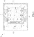
- FIG. 2 is a perspective top view of the PoP package showing side-by-side arrangement of an RF die and a SoC (system-on-a-chip) die and the arrangement of the connection elements disposed around the RF die and the SoC die in the bottom package of the exemplary PoP package in FIG. 1 .
- SoC system-on-a-chip
- the PoP package 1 comprises a bottom package 10 and a top package 20 stacked on the bottom package 10.
- the top package 20 may be a memory package such as a dynamic random access memory (DRAM) package having at least one encapsulated DRAM die such as double data rate 4 (DDR4), low-power DDR4 (LPDDR4), DDR5, LPDDR5 or the like.
- the bottom package 10 may comprise a package substrate 100 having a top surface 100a and a bottom surface 100b.
- an RF die D 1 and a SoC die D 2 are mounted on the top surface 100a of the package substrate 100 in a side-by-side manner.
- the package substrate 100 may be a multi-layer circuit board or a multi-layer wiring board.
- the package substrate 100 may be a two-layer, three-layer, or four-layer circuit board, but is not limited thereto.
- the RF die D 1 and the SoC die D 2 may be flipped chips and may be boned to the package substrate 100 in a flip-chip manner.
- the bumps B 1 on an active surface of the RF die D 1 are electrically connected to corresponding bonding pads 101 on the top surface 100a of the package substrate 100.
- an antenna (not shown) disposed in a printed circuit board or system board (not shown) may be electrically coupled to the RF die D 1 through the interconnect traces 103 and vias 104 in the package substrate 100 and the terminal balls TB disposed on the bottom surface 100b of the package substrate 100.
- the bumps B 2 on an active surface of the SoC die D 2 are electrically connected to corresponding bonding pads 102 on the top surface 100a of the package substrate 100.
- the signals from or to the SoC die D 2 may be transmitted through the interconnect traces 103 and vias 104 in the package substrate 100 and the terminal balls TB disposed on the bottom surface 100b of the package substrate 100.
- the RF die D 1 , the SoC die D 2 and the top surface 100a of the package substrate 100 are encapsulated by a molding compound 110.
- a plurality of connection elements C 1 ⁇ C 5 are disposed on the top surface 100a of the package substrate 100.
- the connection elements C 1 ⁇ C 5 may comprise Cu/Sn balls (Cu cored solder balls), Cu pillars, Cu bumps, Cu vias, through mold vias, or the like.
- the connection elements C 1 ⁇ C 5 are surrounded by the molding compound 110. It is to be understood that the number of rows/columns of the connection elements C 1 ⁇ C 5 in FIG. 2 is for illustration purposes only.
- the SoC die D 2 when viewed from the above, may have a rectangular shape and may have four edges E 1 ⁇ E 4 .
- the connection elements C 1 , C 2 , a portion of the connection elements C 4 and a portion of the connection elements C 5 are arranged around the RF die D 1 .
- the connection elements C 2 and C 3 , the rest of the connection elements C 4 and the rest of the connection elements C 5 are arranged around the SoC die D 2 .
- at least the connection elements C 2 disposed directly between the edge E 1 of the SoC die D 2 and the RF die D 1 are grounded, which may act as shielding balls.
- connection elements C 1 , C 2 and some of the connection elements C 3 may be electrically coupled to ground.
- some of the connection elements C 3 may be electrically coupled to power.
- the function of each of the connection elements C 1 ⁇ C 5 may be designated according design requirements and layout design.
- the connection elements near the central position of each row or column may be grounded.
- the column of the connection elements C 1 may be omitted. Therefore, in FIG. 3 , the PoP package 1a may comprise only connection elements C 2 ⁇ C 5 .
- connection elements C 4 and C 5 may be electrically coupled to the top package 20 through an interposer 120.
- the interposer 120 has re-routed traces 121 and/or fan-out/fan-in pads 122 that match with the ball map of the top package 20.
- the interposer 120 may comprise two or more than two metal layers such as copper layers.
- the interposer 120 may comprise laminate material.
- the interposer 120 may comprise BT (Bismaleimide/Triazine) laminate material.
- the interposer 120 may be a Si interposer and may comprise through silicon vias. It is to be understood that the structure of the interposer 120 shown in the figures is for illustration purposes only.
- the interposer 120 may be a re-distributed layer (RDL) interposer.
- RDL re-distributed layer
- the RF die D 1 may be a millimeter wave (mmw) intermediate-frequency (IF) RF die, but is not limited thereto.
- the SoC die D 2 may be a 5G processor die, but is not limited thereto.
- the SoC die D 2 may comprise interfaces such as Camera Serial Interface (CSI) 301 and/or Display Serial Interface (DSI) 302. These interfaces 301 and 302 are designed for high bandwidth video input (CSI) and output (DSI), which may be arranged on the edges E 3 and E 4 , respectively.
- the SoC die D 2 may further comprise Universal Flash Storage (UFS) interface 303, which is a JEDEC standard for high performance mobile storage devices suitable for next generation data storage.
- UFS Universal Flash Storage
- the UFS interface 303 may be arranged on the edge E 2 .
- the SoC die D 2 may further comprise ABB (analog baseband)/SerDes (Serializer and Deserializer) interface 304 and universal serial bus (USB) 2.0/3.0 interface 305, which may be arranged on the edge E 1 .
- the SoC die D 2 may further comprise DDR interfaces 311 ⁇ 314, which are arranged on the edges E 3 and E 4 , respectively.
- the RF die D 1 is disposed adjacent to the edge E 1 . Therefore, the DDR interfaces 311 ⁇ 314 are arranged on edges E 3 and E 4 that are different from the edge E 1 that is adjacent to and directly faces the RF die D 1 .
- the high-frequency digital signal traces 311a ⁇ 314a in the package substrate 100 which are electrically coupled to the DDR interfaces 311 ⁇ 314 on the edges E 3 and E 4 , respectively, do not intersect with the edge E 1 and do not overlap with the RF die D 1 , when viewed from the above.
- the potential digital signal interference from the high-frequency digital signal traces 311a ⁇ 314a can be blocked by the grounded connection elements C 2 disposed between the edge E 1 of the SoC die D 2 and the RF die D 1 .
- the column of grounded connection elements C 2 (signal interference shielding elements) interposed between the RF die D 1 and the SoC die D 2 can effectively reduce noise.
- FIG. 4 is a schematic partial top view showing a separated ground plane configuration of the exemplary PoP package in FIG. 1 .
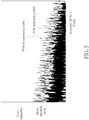
- FIG. 5 is a plot showing noise vs. frequency relationship of the PoP package in FIG. 1 with or without separated ground.
- the ground plane G 1 which may be disposed in the interposer 120, is electrically coupled to connection elements C 1a and is electrically coupled to the RF die D 1 .
- the ground plane G 1 is separated from the DRAM ground plane G 2 in the interposer 120.
- the package substrate 100 may have a separated ground plane for the RF die D 1 .
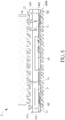
- FIG. 6 is a schematic, cross-sectional diagram showing a PoP package according to another embodiment of the present invention, wherein like numeral numbers designate like elements, regions or layers.
- the PoP package 2 comprises a bottom package 10a and a top package 20 stacked on the bottom package 10a.
- the bottom package 10a may comprise a re-distribution layer (RDL) 400 and the input/output pads on the RF die D 1 and the SoC die D 2 can be re-distributed through the RDL 400 to form bonding pads BP on the lower surface 400b of the RDL 400.
- Terminal balls TB such as ball grid array (BGA) balls are mounted on the respective bonding pads BP.
- BGA ball grid array
- the RF die D 1 and the SoC die D 2 are encapsulated by the molding compound 110 and copper vias V 1 ⁇ V 3 may be formed in the molding compound 110, which are electrically connected to over-mold RDL 420.
- the bonding pads 422 for the top package 20 is formed in the over-mold RDL 420.
- the top package 20 such as LPDDR4 or LPDDR5 DRAM package may be electrically connected to the DDR interface of the SoC die D 2 through the over-mold RDL 420, the copper vias V 1 ⁇ V 3 , and the RDL 400.
- the layout of the copper vias V 2 is similar to the connection elements C 2 as shown in FIG. 2 or FIG. 3 .
- the grounded copper vias V 2 may function as shielding elements that can block the potential digital signal interference from the high-frequency digital signals.
- FIG. 7 is a schematic, cross-sectional diagram showing a PoP package according to still another embodiment of the present invention, wherein like numeral numbers designate like elements, regions or layers.
- the PoP package 3 comprises a bottom package 10b and a top package 20 stacked on the bottom package 10b.
- the bottom package 10b may be an embedded die package.
- the RF die D 1 and the SoC die D 2 are embedded in the substrate and are interconnected through substrate processes so as to form a system-in-board package.
- the RF die D 1 and the SoC die D 2 may be embedded in a core substrate 500.
- the core substrate 500 may comprise copper clad laminate (CCL) substrates or organic laminate substrates known in the art.
- Build-up layers BL and interconnect structures Tr such as high-density interconnect (HDI) traces and laser-drilled vias may be formed on the core substrate 500.
- Through vias PTH 1 ⁇ PTH 3 may be formed in the core substrate 500 of the bottom package 10b and may be electrically coupled to the circuit layer 520.
- the bonding pads 522 for the top package 20 may be formed in the circuit layer 520.
- the top package 20 such as LPDDR4 or LPDDR5 DRAM package may be electrically connected to the DDR interface of the SoC die D 2 through the circuit layer 520, the through vias PTH 1 ⁇ PTH 3 , and the interconnect structures Tr of the substrate 500.
- the layout of the through vias PTH2 is similar to the connection elements C 2 as shown in FIG. 2 or FIG. 3 .
- the grounded through vias PTH2 may function as shielding elements that can block the potential digital signal interference from the high-frequency digital signals.
- FIG. 8 is a schematic, cross-sectional diagram showing a PoP package according to yet another embodiment of the present invention.
- FIG. 9 is a perspective top view of the PoP package showing side-by-side arrangement of the RF die and the SoC die and the arrangement of the connection elements disposed around the RF die and the SoC die in the bottom package of the exemplary PoP package in FIG. 8 .
- the PoP package 4 comprises a bottom package 10c and a top package 20 stacked on the bottom package 10c.
- the top package 20 may be a memory package such as a DRAM package having at least one encapsulated DRAM die such as DDR4, LPDDR4, DDR5, LPDDR5 or the like.
- the bottom package 10c may comprise a package substrate 100 having a top surface 100a and a bottom surface 100b.
- an RF die D 1 and a SoC die D 2 are mounted on the top surface 100a of the package substrate 100 in a side-by-side manner.
- the package substrate 100 may be a multi-layer circuit board or a multi-layer wiring board.
- the package substrate 100 may be a two-layer, three-layer, or four-layer circuit board, but is not limited thereto.
- the RF die D 1 and the SoC die D 2 may be flipped chips and may be boned to the package substrate 100 in a flip-chip manner.
- the RF die D 1 , the SoC die D 2 and the top surface 100a of the package substrate 100 are encapsulated by a molding compound 110.
- a plurality of connection elements C 2 ⁇ C 5 are disposed on the top surface 100a of the package substrate 100.
- the connection elements C 2 ⁇ C 5 may comprise Cu/Sn balls (Cu cored solder balls), Cu pillars, Cu bumps, Cu vias, through mold vias, or the like.
- the connection elements C 2 ⁇ C 5 are surrounded by the molding compound 110.
- the connection elements C 2 ⁇ C 5 may be electrically coupled to the top package 20 through an interposer 120.
- the interposer 120 has re-routed traces and/or fan-out/fan-in pads that match with the ball map of the top package 20.
- the interposer 120 may comprise two or more than two metal layers such as copper layers.
- the interposer 120 may comprise laminate material.
- the interposer 120 may comprise BT (Bismaleimide/Triazine) laminate material.
- the interposer 120 may be a Si interposer and may comprise through silicon vias. It is to be understood that the structure of the interposer 120 shown in the figures is for illustration purposes only.
- the size of the package substrate 100 is greater than the overlying interposer 120. Therefore, only the SoC die D 2 is completely surrounded by the connection elements C 2 ⁇ C 5 . In addition, only the SoC die D 2 is overlapped with the interposer 120.
- the high-frequency digital signal traces in the package substrate 100 which are electrically coupled to the DDR interfaces on the edges E 3 and E 4 , respectively, do not intersect with the edge E 1 and do not overlap with the RF die D 1 .
- the grounded connection elements C 2 may function as shielding elements that can block the potential digital signal interference from the high-frequency digital signals.
Landscapes
- Semiconductor Integrated Circuits (AREA)
- Semiconductor Memories (AREA)
- Physics & Mathematics (AREA)
- Health & Medical Sciences (AREA)
- Electromagnetism (AREA)
- Toxicology (AREA)
- Shielding Devices Or Components To Electric Or Magnetic Fields (AREA)
Abstract
Description
- This application claims benefits from
U.S. provisional application No. 62/719,825 filed August 20, 2018 - The present disclosure relates generally to the field of semiconductor packaging. More particularly, the present disclosure relates to an improved package-on-package (PoP) package with reduced noise to satisfy de-sense requirement, which is suited for the 5G or automotive applications.
- Semiconductor integrated circuit dies or chips are typically packaged for protection against an external environment. The package may provide physical protection, stability, external connections to the die inside the packages. In some cases, a DRAM package may be stacked on a bottom package so as to form a package-on-package (PoP) package.
- However, the interposer substrate, which is disposed between the top package (i.e. DRAM package) and the bottom package, and the high-frequency interconnect traces and/or vias for communication with the DRAM chip, adversely affect the performance of the PoP package, especially when the bottom package comprises a vulnerable radio-frequency (RF) chip.
- It is one object to provide an improved Package-on-Package (PoP) package structure with reduced noise to satisfy de-sense requirement.
- According to one embodiment, a semiconductor package includes a bottom package comprising a substrate, a radio-frequency (RF) die and a system-on-a-chip (SoC) die arranged on the substrate in a side-by-side manner, a molding compound covering the RF die and the SoC die, and an interposer over the molding compound.
- Connection elements and a column of signal interference shielding elements are disposed on the substrate. The connection elements surround the SoC die. The column of signal interference shielding elements is interposed between the RF die and the SoC die. A top package is mounted on the interposer.
- Preferably, the top package is a memory package. According to one embodiment, the memory package is a dynamic random access memory (DRAM) package having at least one encapsulated DRAM die.
- Preferably, the RF die is a millimeter wave (mmw) intermediate-frequency (IF) RF die.
- Preferably, the plurality of connection elements comprise Cu/Sn balls, Cu pillars, Cu bumps, Cu vias, or through mold vias.
- Preferably, the plurality of connection elements and the column of signal interference shielding elements are surrounded by the molding compound.
- Preferably, the plurality of connection elements is coplanar with the column of signal interference shielding elements within the molding compound.
- Preferably, the interposer comprises re-routed traces and/or fan-out/fan-in pads that match with a ball map of the top package.
- Preferably, the interposer comprises a Si interposer.
- Preferably, the interposer comprises a re-distributed layer (RDL) interposer.
- Preferably, the SoC die comprises double data rate (DDR) interfaces arranged on an edge that is different from an edge of the SoC die that is adjacent to and directly faces the RF die.
- Preferably, the SoC die (further) comprises Camera Serial Interface (CSI) and/or Display Serial Interface.
- Preferably, the SoC die (further) comprises Universal Flash Storage (UFS) interface.
- Preferably, the SoC die (further) comprises analog baseband (ABB)/ Serializer and Deserializer (SerDes) interface.
- Preferably, the SoC die (further) comprises universal serial bus (USB) interface.
- Preferably, the RF die is electrically coupled to a ground plane in the interposer that is physically separated from a DRAM ground plane.
- Preferably, the column of signal interference shielding elements are grounded elements.
- These and other objectives of the present invention will no doubt become obvious to those of ordinary skill in the art after reading the following detailed description of the preferred embodiment that is illustrated in the various figures and drawings.
- The accompanying drawings are included to provide a further understanding of the invention, and are incorporated in and constitute a part of this specification. The drawings illustrate embodiments of the invention and, together with the description, serve to explain the principles of the invention. In the drawings:
-
FIG. 1 is a schematic, cross-sectional diagram showing an exemplary PoP package according to one embodiment of the present invention; -
FIG. 2 is a perspective top view of the PoP package showing side-by-side arrangement of an RF die and a SoC die and the arrangement of the connection elements around the RF die and the SoC die in the bottom package of the exemplary PoP package inFIG. 1 ; -
FIG. 3 is a perspective top view of the PoP package showing the arrangement of the connection elements around the RF die and a SoC die according to another embodiment of the present invention; -
FIG. 4 is a schematic partial top view showing a separated ground plane configuration of the exemplary PoP package inFIG. 1 ; -
FIG. 5 is a plot showing noise vs. frequency relationship of the PoP package inFIG. 1 with or without separated ground; -
FIG. 6 is a schematic, cross-sectional diagram showing a PoP package according to another embodiment of the present invention; and -
FIG. 7 is a schematic, cross-sectional diagram showing a PoP package according to still another embodiment of the present invention; -
FIG. 8 is a schematic, cross-sectional diagram showing a PoP package according to yet another embodiment of the present invention; and -
FIG. 9 is a perspective top view of the PoP package showing side-by-side arrangement of the RF die and the SoC die and the arrangement of the connection elements disposed around the RF die and the SoC die in the bottom package of the exemplary PoP package inFIG. 8 . - In the following detailed description of embodiments of the invention, reference is made to the accompanying drawings, which form a part hereof, and in which is shown by way of illustration specific preferred embodiments in which the disclosure may be practiced. These embodiments are described in sufficient detail to enable those skilled in the art to practice them, and it is to be understood that other embodiments may be utilized and that mechanical, structural, and procedural changes may be made without departing from the spirit and scope of the present disclosure. The following detailed description is, therefore, not to be taken in a limiting sense, and the scope of embodiments of the present invention is defined only by the appended claims.
- It will be understood that, although the terms first, second, third, primary, secondary, etc. may be used herein to describe various elements, components, regions, layers and/or sections, these elements, components, regions, layers and/or sections should not be limited by these terms. These terms are only used to distinguish one element, component, region, layer or section from another region, layer or section. Thus, a first or primary element, component, region, layer or section discussed below could be termed a second or secondary element, component, region, layer or section without departing from the teachings of the present inventive concept.
- Spatially relative terms, such as "beneath", "below", "lower", "under", "above," "upper," "over" and the like, may be used herein for ease of description to describe one element or feature's relationship to another element(s) or feature(s) as illustrated in the figures. It will be understood that the spatially relative terms are intended to encompass different orientations of the device in use or operation in addition to the orientation depicted in the figures. For example, if the device in the figures is turned over, elements described as "below" or "beneath" or "under" other elements or features would then be oriented "above" or "over" the other elements or features. Thus, the exemplary terms "below" and "under" can encompass both an orientation of above and below. The device may be otherwise oriented (rotated 90 degrees or at other orientations) and the spatially relative descriptors used herein interpreted accordingly. In addition, it will also be understood that when a layer is referred to as being "between" two layers, it can be the only layer between the two layers, or one or more intervening layers may also be present.
- The terminology used herein is for the purpose of describing particular embodiments only and is not intended to be limiting of the inventive concept. As used herein, the singular forms "a", "an" and "the" are intended to include the plural forms as well, unless the context clearly indicates otherwise. It will be further understood that the terms "comprises" and/or "comprising," when used in this specification, specify the presence of stated features, integers, steps, operations, elements, and/or components, but do not preclude the presence or addition of one or more other features, integers, steps, operations, elements, components, and/or groups thereof. As used herein, the term "and/or" includes any and all combinations of one or more of the associated listed items, and may be abbreviated as "/".
- It will be understood that when an element or layer is referred to as being "on", "connected to", "coupled to", or "adjacent to" another element or layer, it can be directly on, connected, coupled, or adjacent to the other element or layer, or intervening elements or layers may be present. In contrast, when an element is referred to as being "directly on," "directly connected to", "directly coupled to", or "immediately adjacent to" another element or layer, there are no intervening elements or layers present.
- It is noted that: (i) same features throughout the drawing figures will be denoted by the same reference label and are not necessarily described in detail in every drawing that they appear in, and (ii) a sequence of drawings may show different aspects of a single item, each aspect associated with various reference labels that may appear throughout the sequence, or may appear only in selected drawings of the sequence.
- The present disclosure pertains to a semiconductor chip package with reduced noise (< noise threshold level) to satisfy de-sense requirement, which is suited for the 5G (fifth-generation of mobile communication) or automotive applications. Preferably, the semiconductor chip package may be a Package-on-Package (PoP) package including a DRAM package (top package) stacked on a RF-SiP package (bottom package), but is not limited thereto. The electromagnetic interference to the RF chip or die in the bottom RF-SiP package can be alleviated and the in-package noise originated from the high-frequency digital transmissions can be reduced.
- Please refer to
FIG. 1 andFIG. 2 .FIG. 1 is a schematic, cross-sectional diagram showing an exemplary PoP package according to one embodiment of the present invention.FIG. 2 is a perspective top view of the PoP package showing side-by-side arrangement of an RF die and a SoC (system-on-a-chip) die and the arrangement of the connection elements disposed around the RF die and the SoC die in the bottom package of the exemplary PoP package inFIG. 1 . - As shown in
FIG. 1 , according to one exemplary embodiment, thePoP package 1 comprises abottom package 10 and atop package 20 stacked on thebottom package 10. Preferably, thetop package 20 may be a memory package such as a dynamic random access memory (DRAM) package having at least one encapsulated DRAM die such as double data rate 4 (DDR4), low-power DDR4 (LPDDR4), DDR5, LPDDR5 or the like. Preferably, thebottom package 10 may comprise apackage substrate 100 having atop surface 100a and abottom surface 100b. Preferably, an RF die D1 and a SoC die D2 are mounted on thetop surface 100a of thepackage substrate 100 in a side-by-side manner. - Preferably, the
package substrate 100 may be a multi-layer circuit board or a multi-layer wiring board. For example, thepackage substrate 100 may be a two-layer, three-layer, or four-layer circuit board, but is not limited thereto. Preferably, the RF die D1 and the SoC die D2 may be flipped chips and may be boned to thepackage substrate 100 in a flip-chip manner. - For example, the bumps B1 on an active surface of the RF die D1 are electrically connected to
corresponding bonding pads 101 on thetop surface 100a of thepackage substrate 100. For example, an antenna (not shown) disposed in a printed circuit board or system board (not shown) may be electrically coupled to the RF die D1 through the interconnect traces 103 and vias 104 in thepackage substrate 100 and the terminal balls TB disposed on thebottom surface 100b of thepackage substrate 100. For example, the bumps B2 on an active surface of the SoC die D2 are electrically connected tocorresponding bonding pads 102 on thetop surface 100a of thepackage substrate 100. For example, the signals from or to the SoC die D2 may be transmitted through the interconnect traces 103 and vias 104 in thepackage substrate 100 and the terminal balls TB disposed on thebottom surface 100b of thepackage substrate 100. - Preferably, the RF die D1, the SoC die D2 and the
top surface 100a of thepackage substrate 100 are encapsulated by amolding compound 110. Preferably, as shown inFIG. 1 andFIG. 2 , a plurality of connection elements C1∼C5 are disposed on thetop surface 100a of thepackage substrate 100. For example, the connection elements C1∼C5 may comprise Cu/Sn balls (Cu cored solder balls), Cu pillars, Cu bumps, Cu vias, through mold vias, or the like. Preferably, the connection elements C1∼C5 are surrounded by themolding compound 110. It is to be understood that the number of rows/columns of the connection elements C1∼C5 inFIG. 2 is for illustration purposes only. - According to one exemplary embodiment, as shown in
FIG. 2 , when viewed from the above, the SoC die D2 may have a rectangular shape and may have four edges E1∼E4. The connection elements C1, C2, a portion of the connection elements C4 and a portion of the connection elements C5 are arranged around the RF die D1. The connection elements C2 and C3, the rest of the connection elements C4 and the rest of the connection elements C5 are arranged around the SoC die D2. Preferably, at least the connection elements C2 disposed directly between the edge E1 of the SoC die D2 and the RF die D1 are grounded, which may act as shielding balls. Preferably, the connection elements C1, C2 and some of the connection elements C3 may be electrically coupled to ground. Preferably, some of the connection elements C3 may be electrically coupled to power. It is to be understood that the function of each of the connection elements C1∼C5 may be designated according design requirements and layout design. Preferably, the connection elements near the central position of each row or column may be grounded. According to another embodiment, as shown inFIG. 3 , the column of the connection elements C1 may be omitted. Therefore, inFIG. 3 , the PoP package 1a may comprise only connection elements C2∼C5. - Preferably, the connection elements C4 and C5 may be electrically coupled to the
top package 20 through aninterposer 120. Theinterposer 120 has re-routedtraces 121 and/or fan-out/fan-inpads 122 that match with the ball map of thetop package 20. Theinterposer 120 may comprise two or more than two metal layers such as copper layers. Theinterposer 120 may comprise laminate material. For example, theinterposer 120 may comprise BT (Bismaleimide/Triazine) laminate material. Preferably, theinterposer 120 may be a Si interposer and may comprise through silicon vias. It is to be understood that the structure of theinterposer 120 shown in the figures is for illustration purposes only. Preferably, theinterposer 120 may be a re-distributed layer (RDL) interposer. - Preferably, the RF die D1 may be a millimeter wave (mmw) intermediate-frequency (IF) RF die, but is not limited thereto. Preferably, the SoC die D2 may be a 5G processor die, but is not limited thereto. For example, the SoC die D2 may comprise interfaces such as Camera Serial Interface (CSI) 301 and/or Display Serial Interface (DSI) 302. These
interfaces interface 303, which is a JEDEC standard for high performance mobile storage devices suitable for next generation data storage. According to a non-limiting, exemplary embodiment, theUFS interface 303 may be arranged on the edge E2. The SoC die D2 may further comprise ABB (analog baseband)/SerDes (Serializer and Deserializer)interface 304 and universal serial bus (USB) 2.0/3.0interface 305, which may be arranged on the edge E1. The SoC die D2 may further compriseDDR interfaces 311∼314, which are arranged on the edges E3 and E4, respectively. - It is noteworthy that the RF die D1 is disposed adjacent to the edge E1. Therefore, the DDR interfaces 311∼314 are arranged on edges E3 and E4 that are different from the edge E1 that is adjacent to and directly faces the RF die D1. Preferably, the high-frequency digital signal traces 311a∼314a in the
package substrate 100, which are electrically coupled to the DDR interfaces 311∼314 on the edges E3 and E4, respectively, do not intersect with the edge E1 and do not overlap with the RF die D1, when viewed from the above. In addition, the potential digital signal interference from the high-frequency digital signal traces 311a∼314a can be blocked by the grounded connection elements C2 disposed between the edge E1 of the SoC die D2 and the RF die D1. The column of grounded connection elements C2 (signal interference shielding elements) interposed between the RF die D1 and the SoC die D2 can effectively reduce noise. - Please refer to
FIG. 4 andFIG. 5 .FIG. 4 is a schematic partial top view showing a separated ground plane configuration of the exemplary PoP package inFIG. 1 .FIG. 5 is a plot showing noise vs. frequency relationship of the PoP package inFIG. 1 with or without separated ground. As shown inFIG. 4 , the ground plane G1, which may be disposed in theinterposer 120, is electrically coupled to connection elements C1a and is electrically coupled to the RF die D1. The ground plane G1 is separated from the DRAM ground plane G2 in theinterposer 120. By providing such configuration, the noise can be reduced to -170dBm/Hz or even lower as shown inFIG. 5 . In some embodiments, likewise, thepackage substrate 100 may have a separated ground plane for the RF die D1. -
FIG. 6 is a schematic, cross-sectional diagram showing a PoP package according to another embodiment of the present invention, wherein like numeral numbers designate like elements, regions or layers. As shown inFIG. 6 , thePoP package 2 comprises abottom package 10a and atop package 20 stacked on thebottom package 10a. Thebottom package 10a may comprise a re-distribution layer (RDL) 400 and the input/output pads on the RF die D1 and the SoC die D2 can be re-distributed through theRDL 400 to form bonding pads BP on thelower surface 400b of theRDL 400. Terminal balls TB such as ball grid array (BGA) balls are mounted on the respective bonding pads BP. Likewise, the RF die D1 and the SoC die D2 are encapsulated by themolding compound 110 and copper vias V1∼V3 may be formed in themolding compound 110, which are electrically connected to over-moldRDL 420. Thebonding pads 422 for thetop package 20 is formed in theover-mold RDL 420. Thetop package 20 such as LPDDR4 or LPDDR5 DRAM package may be electrically connected to the DDR interface of the SoC die D2 through theover-mold RDL 420, the copper vias V1∼V3, and theRDL 400. The layout of the copper vias V2 is similar to the connection elements C2 as shown inFIG. 2 orFIG. 3 . The grounded copper vias V2 may function as shielding elements that can block the potential digital signal interference from the high-frequency digital signals. -
FIG. 7 is a schematic, cross-sectional diagram showing a PoP package according to still another embodiment of the present invention, wherein like numeral numbers designate like elements, regions or layers. As shown inFIG. 7 , likewise, thePoP package 3 comprises abottom package 10b and atop package 20 stacked on thebottom package 10b. Thebottom package 10b may be an embedded die package. The RF die D1 and the SoC die D2 are embedded in the substrate and are interconnected through substrate processes so as to form a system-in-board package. For example, the RF die D1 and the SoC die D2 may be embedded in acore substrate 500. Thecore substrate 500 may comprise copper clad laminate (CCL) substrates or organic laminate substrates known in the art. Build-up layers BL and interconnect structures Tr such as high-density interconnect (HDI) traces and laser-drilled vias may be formed on thecore substrate 500. Through vias PTH1∼PTH3 may be formed in thecore substrate 500 of thebottom package 10b and may be electrically coupled to thecircuit layer 520. Thebonding pads 522 for thetop package 20 may be formed in thecircuit layer 520. Thetop package 20 such as LPDDR4 or LPDDR5 DRAM package may be electrically connected to the DDR interface of the SoC die D2 through thecircuit layer 520, the through vias PTH1∼PTH3, and the interconnect structures Tr of thesubstrate 500. The layout of the through vias PTH2 is similar to the connection elements C2 as shown inFIG. 2 orFIG. 3 . The grounded through vias PTH2 may function as shielding elements that can block the potential digital signal interference from the high-frequency digital signals. - Please refer to
FIG. 8 andFIG. 9 .FIG. 8 is a schematic, cross-sectional diagram showing a PoP package according to yet another embodiment of the present invention.FIG. 9 is a perspective top view of the PoP package showing side-by-side arrangement of the RF die and the SoC die and the arrangement of the connection elements disposed around the RF die and the SoC die in the bottom package of the exemplary PoP package inFIG. 8 . - As shown in
FIG. 8 , thePoP package 4 comprises abottom package 10c and atop package 20 stacked on thebottom package 10c. Preferably, thetop package 20 may be a memory package such as a DRAM package having at least one encapsulated DRAM die such as DDR4, LPDDR4, DDR5, LPDDR5 or the like. Preferably, thebottom package 10c may comprise apackage substrate 100 having atop surface 100a and abottom surface 100b. Preferably, an RF die D1 and a SoC die D2 are mounted on thetop surface 100a of thepackage substrate 100 in a side-by-side manner. - Preferably, likewise, the
package substrate 100 may be a multi-layer circuit board or a multi-layer wiring board. For example, thepackage substrate 100 may be a two-layer, three-layer, or four-layer circuit board, but is not limited thereto.Preferably, the RF die D1 and the SoC die D2 may be flipped chips and may be boned to thepackage substrate 100 in a flip-chip manner. - Preferably, the RF die D1, the SoC die D2 and the
top surface 100a of thepackage substrate 100 are encapsulated by amolding compound 110. Preferably, as shown inFIG. 8 andFIG. 9 , a plurality of connection elements C2∼C5 are disposed on thetop surface 100a of thepackage substrate 100. For example, the connection elements C2∼C5 may comprise Cu/Sn balls (Cu cored solder balls), Cu pillars, Cu bumps, Cu vias, through mold vias, or the like. Preferably, the connection elements C2∼C5 are surrounded by themolding compound 110. Preferably, the connection elements C2∼C5 may be electrically coupled to thetop package 20 through aninterposer 120. Theinterposer 120 has re-routed traces and/or fan-out/fan-in pads that match with the ball map of thetop package 20. Theinterposer 120 may comprise two or more than two metal layers such as copper layers. Theinterposer 120 may comprise laminate material. For example, theinterposer 120 may comprise BT (Bismaleimide/Triazine) laminate material. Preferably, theinterposer 120 may be a Si interposer and may comprise through silicon vias. It is to be understood that the structure of theinterposer 120 shown in the figures is for illustration purposes only. - The size of the
package substrate 100 is greater than theoverlying interposer 120. Therefore, only the SoC die D2 is completely surrounded by the connection elements C2∼C5. In addition, only the SoC die D2 is overlapped with theinterposer 120. The high-frequency digital signal traces in thepackage substrate 100, which are electrically coupled to the DDR interfaces on the edges E3 and E4, respectively, do not intersect with the edge E1 and do not overlap with the RF die D1. The grounded connection elements C2 may function as shielding elements that can block the potential digital signal interference from the high-frequency digital signals. - Those skilled in the art will readily observe that numerous modifications and alterations of the device and method may be made while retaining the teachings of the invention. Accordingly, the above disclosure should be construed as limited only by the metes and bounds of the appended claims.
Claims (14)
- A semiconductor package, comprising:a bottom package (10) comprising a substrate (100), a radio-frequency, in the following also referred to as RF, die (D1) and a system-on-a-chip, in the following also referred to as SoC, die (D2) arranged on said substrate (100) in a side-by-side manner, a molding compound (110) covering said RF die (D1) and said SoC die (D2), and an interposer (120) over said molding compound (110);a plurality of connection elements (C1∼C5) disposed on a top surface (100a) of said substrate (100), wherein said plurality of connection elements (C1∼C5) surrounds said SoC die (D2);a column of signal interference shielding elements (C2) interposed between said RF die (D1) and said SoC die (D2); anda top package (20) mounted on the interposer (120).
- The semiconductor package according to claim 1, wherein said top package (20) is a memory package.
- The semiconductor package according to claim 2, wherein said memory package is a dynamic random access memory, in the following also referred to as DRAM, package having at least one encapsulated DRAM die.
- The semiconductor package according to any one of claims 1 to 3, wherein said RF die (D1) is a millimeter wave, in the following also referred to as mmw, intermediate-frequency, in the following also referred to as IF, RF die.
- The semiconductor package according to any one of claims 1 to 4, wherein said plurality of connection elements (C1∼C5) comprise Cu/Sn balls, Cu pillars, Cu bumps, Cu vias, or through mold vias.
- The semiconductor package according to any one of claims 1 to 5, wherein said plurality of connection elements (C1∼C5) and said column of signal interference shielding elements (C2) are surrounded by the molding compound (110).
- The semiconductor package according to claim 6, wherein said plurality of connection elements (C1∼C5) is coplanar with said column of signal interference shielding elements (C2) within said molding compound (110).
- The semiconductor package according to any one of claims 1 to 7, wherein said interposer (120) comprises re-routed traces (121) and/or fan-out/fan-in pads (122) that match with a ball map of said top package (20).
- The semiconductor package according to any one of claims 1 to 8, wherein said interposer (120) comprises a Si interposer.
- The semiconductor package according to any one of claims 1 to 9, wherein said interposer (120) comprises a re-distributed layer, in the following also referred to as RDL, interposer.
- The semiconductor package according to any one of claims 1 to 10, wherein said SoC die (D2) comprises double data rate, in the following also referred to as DDR, interfaces (311∼314) arranged on an edge (E3, E4) that is different from an edge (E1) of said SoC die (D2) that is adjacent to and directly faces said RF die (D1).
- The semiconductor package according to any one of claims 1 to 11, wherein said RF die (D1) is electrically coupled to a ground plane (G1) in the interposer (120) that is physically separated from a DRAM ground plane (G2).
- The semiconductor package according to any one of claims 1 to 12, wherein said column of signal interference shielding elements (C2) are grounded elements.
- The semiconductor package according to any one of claims 1 to 13, wherein the signal interference shielding elements (C2) are coupled to ground.
Applications Claiming Priority (2)
| Application Number | Priority Date | Filing Date | Title |
|---|---|---|---|
| US201862719825P | 2018-08-20 | 2018-08-20 | |
| US16/535,019 US10910323B2 (en) | 2018-08-20 | 2019-08-07 | Semiconductor package with reduced noise |
Publications (2)
| Publication Number | Publication Date |
|---|---|
| EP3614427A1 true EP3614427A1 (en) | 2020-02-26 |
| EP3614427B1 EP3614427B1 (en) | 2024-06-19 |
Family
ID=67659252
Family Applications (1)
| Application Number | Title | Priority Date | Filing Date |
|---|---|---|---|
| EP19192261.6A Active EP3614427B1 (en) | 2018-08-20 | 2019-08-19 | Semiconductor package with reduced noise |
Country Status (2)
| Country | Link |
|---|---|
| US (1) | US10910323B2 (en) |
| EP (1) | EP3614427B1 (en) |
Families Citing this family (2)
| Publication number | Priority date | Publication date | Assignee | Title |
|---|---|---|---|---|
| CN114759015B (en) * | 2022-03-02 | 2023-06-02 | 中国电子科技集团公司第二十九研究所 | Three-dimensional stacking integrated structure of high-power radio frequency chip and preparation method thereof |
| CN115274632B (en) * | 2022-07-01 | 2025-12-09 | 北京遥测技术研究所 | Multichannel receiving and transmitting integrated high-density inner bump sip device |
Citations (7)
| Publication number | Priority date | Publication date | Assignee | Title |
|---|---|---|---|---|
| US20090284947A1 (en) * | 2008-05-19 | 2009-11-19 | Stanley Craig Beddingfield | Integrated circuit package having integrated faraday shield |
| US20120086109A1 (en) * | 2010-10-07 | 2012-04-12 | Samsung Electronics Co., Ltd. | Semiconductor Device Including Shielding Layer And Fabrication Method Thereof |
| US20150333401A1 (en) * | 2013-06-26 | 2015-11-19 | Saravana Maruthamuthu | Bulk acoustic wave resonator tuner circuits |
| US20170243858A1 (en) * | 2013-10-04 | 2017-08-24 | Mediatek Inc. | Semiconductor package incorporating redistribution layer interposer |
| US20180076175A1 (en) * | 2016-09-09 | 2018-03-15 | Taiwan Semiconductor Manufacturing Company, Ltd. | Redistribution Layers in Semiconductor Packages and Methods of Forming Same |
| US20180115051A1 (en) * | 2016-10-21 | 2018-04-26 | Echostar Technologies L.L.C. | Rf antenna arrangement configured to be a part of a lid to an apparatus |
| US20180166405A1 (en) * | 2016-12-13 | 2018-06-14 | Taiwan Semiconductor Manufacturing Co. Ltd. | Structure and formation method of chip package with antenna element |
Family Cites Families (4)
| Publication number | Priority date | Publication date | Assignee | Title |
|---|---|---|---|---|
| SG2013083258A (en) | 2013-11-06 | 2015-06-29 | Thales Solutions Asia Pte Ltd | A guard structure for signal isolation |
| US10418332B2 (en) * | 2017-03-13 | 2019-09-17 | STATS ChipPAC Pte. Ltd. | Semiconductor device and method of forming partition fence and shielding layer around semiconductor components |
| US11322449B2 (en) * | 2017-10-31 | 2022-05-03 | Taiwan Semiconductor Manufacturing Co., Ltd. | Package with fan-out structures |
| US10468355B2 (en) | 2017-12-08 | 2019-11-05 | Taiwan Semiconductor Manufacturing Company, Ltd. | EMI Shielding structure in InFO package |
-
2019
- 2019-08-07 US US16/535,019 patent/US10910323B2/en active Active
- 2019-08-19 EP EP19192261.6A patent/EP3614427B1/en active Active
Patent Citations (7)
| Publication number | Priority date | Publication date | Assignee | Title |
|---|---|---|---|---|
| US20090284947A1 (en) * | 2008-05-19 | 2009-11-19 | Stanley Craig Beddingfield | Integrated circuit package having integrated faraday shield |
| US20120086109A1 (en) * | 2010-10-07 | 2012-04-12 | Samsung Electronics Co., Ltd. | Semiconductor Device Including Shielding Layer And Fabrication Method Thereof |
| US20150333401A1 (en) * | 2013-06-26 | 2015-11-19 | Saravana Maruthamuthu | Bulk acoustic wave resonator tuner circuits |
| US20170243858A1 (en) * | 2013-10-04 | 2017-08-24 | Mediatek Inc. | Semiconductor package incorporating redistribution layer interposer |
| US20180076175A1 (en) * | 2016-09-09 | 2018-03-15 | Taiwan Semiconductor Manufacturing Company, Ltd. | Redistribution Layers in Semiconductor Packages and Methods of Forming Same |
| US20180115051A1 (en) * | 2016-10-21 | 2018-04-26 | Echostar Technologies L.L.C. | Rf antenna arrangement configured to be a part of a lid to an apparatus |
| US20180166405A1 (en) * | 2016-12-13 | 2018-06-14 | Taiwan Semiconductor Manufacturing Co. Ltd. | Structure and formation method of chip package with antenna element |
Non-Patent Citations (1)
| Title |
|---|
| KIM SEIL ET AL: "Simulation-based analysis on EMI effect in LPDDR interface for mitigating RFI in a mobile environment", 2016 IEEE 20TH WORKSHOP ON SIGNAL AND POWER INTEGRITY (SPI), IEEE, 8 May 2016 (2016-05-08), pages 1 - 4, XP032914971, DOI: 10.1109/SAPIW.2016.7496263 * |
Also Published As
| Publication number | Publication date |
|---|---|
| US10910323B2 (en) | 2021-02-02 |
| US20200058633A1 (en) | 2020-02-20 |
| EP3614427B1 (en) | 2024-06-19 |
Similar Documents
| Publication | Publication Date | Title |
|---|---|---|
| US9811122B2 (en) | Package on packages and mobile computing devices having the same | |
| US6734539B2 (en) | Stacked module package | |
| US10943878B2 (en) | Semiconductor package | |
| TWI699864B (en) | Antenna module | |
| KR102627223B1 (en) | Antenna module and electronic system including the same | |
| US20140124907A1 (en) | Semiconductor packages | |
| US12021068B2 (en) | Semiconductor device with dummy thermal features on interposer | |
| US20140021591A1 (en) | Emi shielding semiconductor element and semiconductor stack structure | |
| US10332821B2 (en) | Partially molded direct chip attach package structures for connectivity module solutions | |
| US9431361B2 (en) | Ball arrangement for integrated circuit package devices | |
| US20150282367A1 (en) | Electronic assembly that includes stacked electronic components | |
| US10872880B2 (en) | Land grid array package extension | |
| US10103088B1 (en) | Integrated antenna for direct chip attach connectivity module package structures | |
| US20200098727A1 (en) | Stacked wire-bond dice attached by pillars or bumps above a flip-chip die on a semiconductor package substrate | |
| US20140374900A1 (en) | Semiconductor package and method of fabricating the same | |
| EP4135032A1 (en) | Semiconductor package with reduced connection length | |
| WO2018174869A1 (en) | Multiple die package using an embedded bridge connecting dies | |
| US10910323B2 (en) | Semiconductor package with reduced noise | |
| US11227854B2 (en) | Semiconductor package | |
| CN112349702B (en) | Semiconductor packaging | |
| US20140146507A1 (en) | Circuit board and semiconductor device including the same | |
| US9508690B2 (en) | Semiconductor TSV device package for circuit board connection | |
| US11322474B2 (en) | Semiconductor package | |
| EP4343843A1 (en) | Multi-die package on package | |
| US20240339436A1 (en) | Stack packages |
Legal Events
| Date | Code | Title | Description |
|---|---|---|---|
| PUAI | Public reference made under article 153(3) epc to a published international application that has entered the european phase |
Free format text: ORIGINAL CODE: 0009012 |
|
| STAA | Information on the status of an ep patent application or granted ep patent |
Free format text: STATUS: THE APPLICATION HAS BEEN PUBLISHED |
|
| AK | Designated contracting states |
Kind code of ref document: A1 Designated state(s): AL AT BE BG CH CY CZ DE DK EE ES FI FR GB GR HR HU IE IS IT LI LT LU LV MC MK MT NL NO PL PT RO RS SE SI SK SM TR |
|
| AX | Request for extension of the european patent |
Extension state: BA ME |
|
| STAA | Information on the status of an ep patent application or granted ep patent |
Free format text: STATUS: REQUEST FOR EXAMINATION WAS MADE |
|
| 17P | Request for examination filed |
Effective date: 20200724 |
|
| RBV | Designated contracting states (corrected) |
Designated state(s): AL AT BE BG CH CY CZ DE DK EE ES FI FR GB GR HR HU IE IS IT LI LT LU LV MC MK MT NL NO PL PT RO RS SE SI SK SM TR |
|
| STAA | Information on the status of an ep patent application or granted ep patent |
Free format text: STATUS: EXAMINATION IS IN PROGRESS |
|
| 17Q | First examination report despatched |
Effective date: 20230103 |
|
| P01 | Opt-out of the competence of the unified patent court (upc) registered |
Effective date: 20230607 |
|
| RIC1 | Information provided on ipc code assigned before grant |
Ipc: H01L 25/10 20060101ALI20231121BHEP Ipc: H01L 25/18 20060101ALI20231121BHEP Ipc: H01L 23/538 20060101ALI20231121BHEP Ipc: H01L 23/552 20060101ALI20231121BHEP Ipc: H01L 23/66 20060101AFI20231121BHEP |
|
| GRAP | Despatch of communication of intention to grant a patent |
Free format text: ORIGINAL CODE: EPIDOSNIGR1 |
|
| STAA | Information on the status of an ep patent application or granted ep patent |
Free format text: STATUS: GRANT OF PATENT IS INTENDED |
|
| INTG | Intention to grant announced |
Effective date: 20240117 |
|
| GRAS | Grant fee paid |
Free format text: ORIGINAL CODE: EPIDOSNIGR3 |
|
| GRAA | (expected) grant |
Free format text: ORIGINAL CODE: 0009210 |
|
| STAA | Information on the status of an ep patent application or granted ep patent |
Free format text: STATUS: THE PATENT HAS BEEN GRANTED |
|
| AK | Designated contracting states |
Kind code of ref document: B1 Designated state(s): AL AT BE BG CH CY CZ DE DK EE ES FI FR GB GR HR HU IE IS IT LI LT LU LV MC MK MT NL NO PL PT RO RS SE SI SK SM TR |
|
| REG | Reference to a national code |
Ref country code: GB Ref legal event code: FG4D |
|
| REG | Reference to a national code |
Ref country code: CH Ref legal event code: EP |
|
| REG | Reference to a national code |
Ref country code: DE Ref legal event code: R096 Ref document number: 602019053820 Country of ref document: DE |
|
| PG25 | Lapsed in a contracting state [announced via postgrant information from national office to epo] |
Ref country code: BG Free format text: LAPSE BECAUSE OF FAILURE TO SUBMIT A TRANSLATION OF THE DESCRIPTION OR TO PAY THE FEE WITHIN THE PRESCRIBED TIME-LIMIT Effective date: 20240619 |
|
| PG25 | Lapsed in a contracting state [announced via postgrant information from national office to epo] |
Ref country code: FI Free format text: LAPSE BECAUSE OF FAILURE TO SUBMIT A TRANSLATION OF THE DESCRIPTION OR TO PAY THE FEE WITHIN THE PRESCRIBED TIME-LIMIT Effective date: 20240619 Ref country code: HR Free format text: LAPSE BECAUSE OF FAILURE TO SUBMIT A TRANSLATION OF THE DESCRIPTION OR TO PAY THE FEE WITHIN THE PRESCRIBED TIME-LIMIT Effective date: 20240619 |
|
| REG | Reference to a national code |
Ref country code: LT Ref legal event code: MG9D |
|
| PG25 | Lapsed in a contracting state [announced via postgrant information from national office to epo] |
Ref country code: GR Free format text: LAPSE BECAUSE OF FAILURE TO SUBMIT A TRANSLATION OF THE DESCRIPTION OR TO PAY THE FEE WITHIN THE PRESCRIBED TIME-LIMIT Effective date: 20240920 |
|
| REG | Reference to a national code |
Ref country code: NL Ref legal event code: MP Effective date: 20240619 |
|
| PG25 | Lapsed in a contracting state [announced via postgrant information from national office to epo] |
Ref country code: LV Free format text: LAPSE BECAUSE OF FAILURE TO SUBMIT A TRANSLATION OF THE DESCRIPTION OR TO PAY THE FEE WITHIN THE PRESCRIBED TIME-LIMIT Effective date: 20240619 |
|
| PG25 | Lapsed in a contracting state [announced via postgrant information from national office to epo] |
Ref country code: NO Free format text: LAPSE BECAUSE OF FAILURE TO SUBMIT A TRANSLATION OF THE DESCRIPTION OR TO PAY THE FEE WITHIN THE PRESCRIBED TIME-LIMIT Effective date: 20240919 Ref country code: LV Free format text: LAPSE BECAUSE OF FAILURE TO SUBMIT A TRANSLATION OF THE DESCRIPTION OR TO PAY THE FEE WITHIN THE PRESCRIBED TIME-LIMIT Effective date: 20240619 Ref country code: HR Free format text: LAPSE BECAUSE OF FAILURE TO SUBMIT A TRANSLATION OF THE DESCRIPTION OR TO PAY THE FEE WITHIN THE PRESCRIBED TIME-LIMIT Effective date: 20240619 Ref country code: GR Free format text: LAPSE BECAUSE OF FAILURE TO SUBMIT A TRANSLATION OF THE DESCRIPTION OR TO PAY THE FEE WITHIN THE PRESCRIBED TIME-LIMIT Effective date: 20240920 Ref country code: FI Free format text: LAPSE BECAUSE OF FAILURE TO SUBMIT A TRANSLATION OF THE DESCRIPTION OR TO PAY THE FEE WITHIN THE PRESCRIBED TIME-LIMIT Effective date: 20240619 Ref country code: BG Free format text: LAPSE BECAUSE OF FAILURE TO SUBMIT A TRANSLATION OF THE DESCRIPTION OR TO PAY THE FEE WITHIN THE PRESCRIBED TIME-LIMIT Effective date: 20240619 Ref country code: RS Free format text: LAPSE BECAUSE OF FAILURE TO SUBMIT A TRANSLATION OF THE DESCRIPTION OR TO PAY THE FEE WITHIN THE PRESCRIBED TIME-LIMIT Effective date: 20240919 |
|
| PG25 | Lapsed in a contracting state [announced via postgrant information from national office to epo] |
Ref country code: NL Free format text: LAPSE BECAUSE OF FAILURE TO SUBMIT A TRANSLATION OF THE DESCRIPTION OR TO PAY THE FEE WITHIN THE PRESCRIBED TIME-LIMIT Effective date: 20240619 |
|
| REG | Reference to a national code |
Ref country code: AT Ref legal event code: MK05 Ref document number: 1696518 Country of ref document: AT Kind code of ref document: T Effective date: 20240619 |
|
| PG25 | Lapsed in a contracting state [announced via postgrant information from national office to epo] |
Ref country code: NL Free format text: LAPSE BECAUSE OF FAILURE TO SUBMIT A TRANSLATION OF THE DESCRIPTION OR TO PAY THE FEE WITHIN THE PRESCRIBED TIME-LIMIT Effective date: 20240619 |
|
| PG25 | Lapsed in a contracting state [announced via postgrant information from national office to epo] |
Ref country code: PT Free format text: LAPSE BECAUSE OF FAILURE TO SUBMIT A TRANSLATION OF THE DESCRIPTION OR TO PAY THE FEE WITHIN THE PRESCRIBED TIME-LIMIT Effective date: 20241021 |
|
| PG25 | Lapsed in a contracting state [announced via postgrant information from national office to epo] |
Ref country code: PT Free format text: LAPSE BECAUSE OF FAILURE TO SUBMIT A TRANSLATION OF THE DESCRIPTION OR TO PAY THE FEE WITHIN THE PRESCRIBED TIME-LIMIT Effective date: 20241021 |
|
| PG25 | Lapsed in a contracting state [announced via postgrant information from national office to epo] |
Ref country code: PL Free format text: LAPSE BECAUSE OF FAILURE TO SUBMIT A TRANSLATION OF THE DESCRIPTION OR TO PAY THE FEE WITHIN THE PRESCRIBED TIME-LIMIT Effective date: 20240619 |
|
| PG25 | Lapsed in a contracting state [announced via postgrant information from national office to epo] |
Ref country code: EE Free format text: LAPSE BECAUSE OF FAILURE TO SUBMIT A TRANSLATION OF THE DESCRIPTION OR TO PAY THE FEE WITHIN THE PRESCRIBED TIME-LIMIT Effective date: 20240619 |
|
| PG25 | Lapsed in a contracting state [announced via postgrant information from national office to epo] |
Ref country code: AT Free format text: LAPSE BECAUSE OF FAILURE TO SUBMIT A TRANSLATION OF THE DESCRIPTION OR TO PAY THE FEE WITHIN THE PRESCRIBED TIME-LIMIT Effective date: 20240619 Ref country code: IS Free format text: LAPSE BECAUSE OF FAILURE TO SUBMIT A TRANSLATION OF THE DESCRIPTION OR TO PAY THE FEE WITHIN THE PRESCRIBED TIME-LIMIT Effective date: 20241019 |
|
| PG25 | Lapsed in a contracting state [announced via postgrant information from national office to epo] |
Ref country code: CZ Free format text: LAPSE BECAUSE OF FAILURE TO SUBMIT A TRANSLATION OF THE DESCRIPTION OR TO PAY THE FEE WITHIN THE PRESCRIBED TIME-LIMIT Effective date: 20240619 |
|
| PG25 | Lapsed in a contracting state [announced via postgrant information from national office to epo] |
Ref country code: SK Free format text: LAPSE BECAUSE OF FAILURE TO SUBMIT A TRANSLATION OF THE DESCRIPTION OR TO PAY THE FEE WITHIN THE PRESCRIBED TIME-LIMIT Effective date: 20240619 Ref country code: RO Free format text: LAPSE BECAUSE OF FAILURE TO SUBMIT A TRANSLATION OF THE DESCRIPTION OR TO PAY THE FEE WITHIN THE PRESCRIBED TIME-LIMIT Effective date: 20240619 |
|
| PG25 | Lapsed in a contracting state [announced via postgrant information from national office to epo] |
Ref country code: ES Free format text: LAPSE BECAUSE OF FAILURE TO SUBMIT A TRANSLATION OF THE DESCRIPTION OR TO PAY THE FEE WITHIN THE PRESCRIBED TIME-LIMIT Effective date: 20240619 Ref country code: SM Free format text: LAPSE BECAUSE OF FAILURE TO SUBMIT A TRANSLATION OF THE DESCRIPTION OR TO PAY THE FEE WITHIN THE PRESCRIBED TIME-LIMIT Effective date: 20240619 |
|
| PG25 | Lapsed in a contracting state [announced via postgrant information from national office to epo] |
Ref country code: SM Free format text: LAPSE BECAUSE OF FAILURE TO SUBMIT A TRANSLATION OF THE DESCRIPTION OR TO PAY THE FEE WITHIN THE PRESCRIBED TIME-LIMIT Effective date: 20240619 Ref country code: SK Free format text: LAPSE BECAUSE OF FAILURE TO SUBMIT A TRANSLATION OF THE DESCRIPTION OR TO PAY THE FEE WITHIN THE PRESCRIBED TIME-LIMIT Effective date: 20240619 Ref country code: RO Free format text: LAPSE BECAUSE OF FAILURE TO SUBMIT A TRANSLATION OF THE DESCRIPTION OR TO PAY THE FEE WITHIN THE PRESCRIBED TIME-LIMIT Effective date: 20240619 Ref country code: PL Free format text: LAPSE BECAUSE OF FAILURE TO SUBMIT A TRANSLATION OF THE DESCRIPTION OR TO PAY THE FEE WITHIN THE PRESCRIBED TIME-LIMIT Effective date: 20240619 Ref country code: IS Free format text: LAPSE BECAUSE OF FAILURE TO SUBMIT A TRANSLATION OF THE DESCRIPTION OR TO PAY THE FEE WITHIN THE PRESCRIBED TIME-LIMIT Effective date: 20241019 Ref country code: ES Free format text: LAPSE BECAUSE OF FAILURE TO SUBMIT A TRANSLATION OF THE DESCRIPTION OR TO PAY THE FEE WITHIN THE PRESCRIBED TIME-LIMIT Effective date: 20240619 Ref country code: EE Free format text: LAPSE BECAUSE OF FAILURE TO SUBMIT A TRANSLATION OF THE DESCRIPTION OR TO PAY THE FEE WITHIN THE PRESCRIBED TIME-LIMIT Effective date: 20240619 Ref country code: CZ Free format text: LAPSE BECAUSE OF FAILURE TO SUBMIT A TRANSLATION OF THE DESCRIPTION OR TO PAY THE FEE WITHIN THE PRESCRIBED TIME-LIMIT Effective date: 20240619 Ref country code: AT Free format text: LAPSE BECAUSE OF FAILURE TO SUBMIT A TRANSLATION OF THE DESCRIPTION OR TO PAY THE FEE WITHIN THE PRESCRIBED TIME-LIMIT Effective date: 20240619 |
|
| PG25 | Lapsed in a contracting state [announced via postgrant information from national office to epo] |
Ref country code: IT Free format text: LAPSE BECAUSE OF FAILURE TO SUBMIT A TRANSLATION OF THE DESCRIPTION OR TO PAY THE FEE WITHIN THE PRESCRIBED TIME-LIMIT Effective date: 20240619 |
|
| REG | Reference to a national code |
Ref country code: DE Ref legal event code: R097 Ref document number: 602019053820 Country of ref document: DE |
|
| REG | Reference to a national code |
Ref country code: CH Ref legal event code: PL |
|
| PG25 | Lapsed in a contracting state [announced via postgrant information from national office to epo] |
Ref country code: DK Free format text: LAPSE BECAUSE OF FAILURE TO SUBMIT A TRANSLATION OF THE DESCRIPTION OR TO PAY THE FEE WITHIN THE PRESCRIBED TIME-LIMIT Effective date: 20240619 |
|
| PG25 | Lapsed in a contracting state [announced via postgrant information from national office to epo] |
Ref country code: LU Free format text: LAPSE BECAUSE OF NON-PAYMENT OF DUE FEES Effective date: 20240819 |
|
| PG25 | Lapsed in a contracting state [announced via postgrant information from national office to epo] |
Ref country code: CH Free format text: LAPSE BECAUSE OF NON-PAYMENT OF DUE FEES Effective date: 20240831 Ref country code: MC Free format text: LAPSE BECAUSE OF FAILURE TO SUBMIT A TRANSLATION OF THE DESCRIPTION OR TO PAY THE FEE WITHIN THE PRESCRIBED TIME-LIMIT Effective date: 20240619 |
|
| PLBE | No opposition filed within time limit |
Free format text: ORIGINAL CODE: 0009261 |
|
| STAA | Information on the status of an ep patent application or granted ep patent |
Free format text: STATUS: NO OPPOSITION FILED WITHIN TIME LIMIT |
|
| 26N | No opposition filed |
Effective date: 20250320 |
|
| REG | Reference to a national code |
Ref country code: BE Ref legal event code: MM Effective date: 20240831 |
|
| PGFP | Annual fee paid to national office [announced via postgrant information from national office to epo] |
Ref country code: GB Payment date: 20250626 Year of fee payment: 7 |
|
| PG25 | Lapsed in a contracting state [announced via postgrant information from national office to epo] |
Ref country code: BE Free format text: LAPSE BECAUSE OF NON-PAYMENT OF DUE FEES Effective date: 20240831 |
|
| PGFP | Annual fee paid to national office [announced via postgrant information from national office to epo] |
Ref country code: FR Payment date: 20250610 Year of fee payment: 7 |
|
| PG25 | Lapsed in a contracting state [announced via postgrant information from national office to epo] |
Ref country code: IE Free format text: LAPSE BECAUSE OF NON-PAYMENT OF DUE FEES Effective date: 20240819 |
|
| PG25 | Lapsed in a contracting state [announced via postgrant information from national office to epo] |
Ref country code: SE Free format text: LAPSE BECAUSE OF FAILURE TO SUBMIT A TRANSLATION OF THE DESCRIPTION OR TO PAY THE FEE WITHIN THE PRESCRIBED TIME-LIMIT Effective date: 20240619 |
|
| PGFP | Annual fee paid to national office [announced via postgrant information from national office to epo] |
Ref country code: DE Payment date: 20250624 Year of fee payment: 7 |
|
| REG | Reference to a national code |
Ref country code: DE Ref legal event code: R079 Ref document number: 602019053820 Country of ref document: DE Free format text: PREVIOUS MAIN CLASS: H01L0023660000 Ipc: H10W0044200000 |
|
| PG25 | Lapsed in a contracting state [announced via postgrant information from national office to epo] |
Ref country code: CY Free format text: LAPSE BECAUSE OF FAILURE TO SUBMIT A TRANSLATION OF THE DESCRIPTION OR TO PAY THE FEE WITHIN THE PRESCRIBED TIME-LIMIT; INVALID AB INITIO Effective date: 20190819 |
|
| PG25 | Lapsed in a contracting state [announced via postgrant information from national office to epo] |
Ref country code: HU Free format text: LAPSE BECAUSE OF FAILURE TO SUBMIT A TRANSLATION OF THE DESCRIPTION OR TO PAY THE FEE WITHIN THE PRESCRIBED TIME-LIMIT; INVALID AB INITIO Effective date: 20190819 |