EP3614413A1 - Silicon carbide detectors with improved reliability for photon and/or ion beams - Google Patents
Silicon carbide detectors with improved reliability for photon and/or ion beams Download PDFInfo
- Publication number
- EP3614413A1 EP3614413A1 EP18190666.0A EP18190666A EP3614413A1 EP 3614413 A1 EP3614413 A1 EP 3614413A1 EP 18190666 A EP18190666 A EP 18190666A EP 3614413 A1 EP3614413 A1 EP 3614413A1
- Authority
- EP
- European Patent Office
- Prior art keywords
- electrically active
- photon
- ion beam
- active membrane
- electrodes
- Prior art date
- Legal status (The legal status is an assumption and is not a legal conclusion. Google has not performed a legal analysis and makes no representation as to the accuracy of the status listed.)
- Withdrawn
Links
- HBMJWWWQQXIZIP-UHFFFAOYSA-N silicon carbide Chemical compound [Si+]#[C-] HBMJWWWQQXIZIP-UHFFFAOYSA-N 0.000 title claims abstract description 23
- 229910010271 silicon carbide Inorganic materials 0.000 title claims abstract description 23
- 238000010884 ion-beam technique Methods 0.000 title claims abstract description 15
- OKTJSMMVPCPJKN-UHFFFAOYSA-N Carbon Chemical compound [C] OKTJSMMVPCPJKN-UHFFFAOYSA-N 0.000 claims abstract description 33
- 239000012528 membrane Substances 0.000 claims abstract description 29
- 229910052799 carbon Inorganic materials 0.000 claims abstract description 22
- 239000000758 substrate Substances 0.000 claims abstract description 16
- 230000004913 activation Effects 0.000 claims abstract description 4
- 229910003460 diamond Inorganic materials 0.000 claims description 17
- 239000010432 diamond Substances 0.000 claims description 17
- 229910002804 graphite Inorganic materials 0.000 claims description 7
- 239000010439 graphite Substances 0.000 claims description 7
- 230000017525 heat dissipation Effects 0.000 claims description 6
- 229910003481 amorphous carbon Inorganic materials 0.000 claims description 2
- 238000012544 monitoring process Methods 0.000 claims description 2
- 230000008901 benefit Effects 0.000 abstract description 5
- 230000009467 reduction Effects 0.000 abstract description 5
- 241001507928 Aria Species 0.000 abstract description 2
- 235000004494 Sorbus aria Nutrition 0.000 abstract description 2
- 238000000926 separation method Methods 0.000 abstract description 2
- 239000010410 layer Substances 0.000 description 26
- 239000000463 material Substances 0.000 description 6
- 229910052751 metal Inorganic materials 0.000 description 6
- 239000002184 metal Substances 0.000 description 6
- 229910021389 graphene Inorganic materials 0.000 description 5
- PXHVJJICTQNCMI-UHFFFAOYSA-N Nickel Chemical compound [Ni] PXHVJJICTQNCMI-UHFFFAOYSA-N 0.000 description 4
- 229910052782 aluminium Inorganic materials 0.000 description 3
- XAGFODPZIPBFFR-UHFFFAOYSA-N aluminium Chemical compound [Al] XAGFODPZIPBFFR-UHFFFAOYSA-N 0.000 description 3
- 230000005540 biological transmission Effects 0.000 description 3
- 239000013078 crystal Substances 0.000 description 3
- 150000002500 ions Chemical class 0.000 description 3
- 230000003287 optical effect Effects 0.000 description 3
- 238000010521 absorption reaction Methods 0.000 description 2
- 230000008021 deposition Effects 0.000 description 2
- 238000000151 deposition Methods 0.000 description 2
- 229910052759 nickel Inorganic materials 0.000 description 2
- 239000011241 protective layer Substances 0.000 description 2
- 230000004044 response Effects 0.000 description 2
- 238000004088 simulation Methods 0.000 description 2
- 235000012431 wafers Nutrition 0.000 description 2
- 230000015556 catabolic process Effects 0.000 description 1
- 238000006731 degradation reaction Methods 0.000 description 1
- 230000001419 dependent effect Effects 0.000 description 1
- 230000006866 deterioration Effects 0.000 description 1
- 238000009792 diffusion process Methods 0.000 description 1
- 238000006073 displacement reaction Methods 0.000 description 1
- 230000005684 electric field Effects 0.000 description 1
- 238000000407 epitaxy Methods 0.000 description 1
- 238000005530 etching Methods 0.000 description 1
- 230000004907 flux Effects 0.000 description 1
- 239000003574 free electron Substances 0.000 description 1
- 230000008018 melting Effects 0.000 description 1
- 238000002844 melting Methods 0.000 description 1
- 238000000034 method Methods 0.000 description 1
- 230000008569 process Effects 0.000 description 1
- 230000001681 protective effect Effects 0.000 description 1
- 229920006395 saturated elastomer Polymers 0.000 description 1
Images


Classifications
-
- H—ELECTRICITY
- H01—ELECTRIC ELEMENTS
- H01J—ELECTRIC DISCHARGE TUBES OR DISCHARGE LAMPS
- H01J37/00—Discharge tubes with provision for introducing objects or material to be exposed to the discharge, e.g. for the purpose of examination or processing thereof
- H01J37/02—Details
- H01J37/244—Detectors; Associated components or circuits therefor
-
- G—PHYSICS
- G01—MEASURING; TESTING
- G01T—MEASUREMENT OF NUCLEAR OR X-RADIATION
- G01T1/00—Measuring X-radiation, gamma radiation, corpuscular radiation, or cosmic radiation
- G01T1/16—Measuring radiation intensity
- G01T1/26—Measuring radiation intensity with resistance detectors
-
- G—PHYSICS
- G01—MEASURING; TESTING
- G01T—MEASUREMENT OF NUCLEAR OR X-RADIATION
- G01T1/00—Measuring X-radiation, gamma radiation, corpuscular radiation, or cosmic radiation
- G01T1/29—Measurement performed on radiation beams, e.g. position or section of the beam; Measurement of spatial distribution of radiation
-
- H—ELECTRICITY
- H10—SEMICONDUCTOR DEVICES; ELECTRIC SOLID-STATE DEVICES NOT OTHERWISE PROVIDED FOR
- H10F—INORGANIC SEMICONDUCTOR DEVICES SENSITIVE TO INFRARED RADIATION, LIGHT, ELECTROMAGNETIC RADIATION OF SHORTER WAVELENGTH OR CORPUSCULAR RADIATION
- H10F30/00—Individual radiation-sensitive semiconductor devices in which radiation controls the flow of current through the devices, e.g. photodetectors
- H10F30/301—Individual radiation-sensitive semiconductor devices in which radiation controls the flow of current through the devices, e.g. photodetectors the devices being sensitive to very short wavelength, e.g. being sensitive to X-rays, gamma-rays or corpuscular radiation
-
- H—ELECTRICITY
- H10—SEMICONDUCTOR DEVICES; ELECTRIC SOLID-STATE DEVICES NOT OTHERWISE PROVIDED FOR
- H10F—INORGANIC SEMICONDUCTOR DEVICES SENSITIVE TO INFRARED RADIATION, LIGHT, ELECTROMAGNETIC RADIATION OF SHORTER WAVELENGTH OR CORPUSCULAR RADIATION
- H10F77/00—Constructional details of devices covered by this subclass
- H10F77/10—Semiconductor bodies
- H10F77/12—Active materials
- H10F77/122—Active materials comprising only Group IV materials
- H10F77/1226—Active materials comprising only Group IV materials comprising multiple Group IV elements, e.g. SiC
-
- H—ELECTRICITY
- H10—SEMICONDUCTOR DEVICES; ELECTRIC SOLID-STATE DEVICES NOT OTHERWISE PROVIDED FOR
- H10F—INORGANIC SEMICONDUCTOR DEVICES SENSITIVE TO INFRARED RADIATION, LIGHT, ELECTROMAGNETIC RADIATION OF SHORTER WAVELENGTH OR CORPUSCULAR RADIATION
- H10F77/00—Constructional details of devices covered by this subclass
- H10F77/30—Coatings
-
- H—ELECTRICITY
- H10—SEMICONDUCTOR DEVICES; ELECTRIC SOLID-STATE DEVICES NOT OTHERWISE PROVIDED FOR
- H10F—INORGANIC SEMICONDUCTOR DEVICES SENSITIVE TO INFRARED RADIATION, LIGHT, ELECTROMAGNETIC RADIATION OF SHORTER WAVELENGTH OR CORPUSCULAR RADIATION
- H10F77/00—Constructional details of devices covered by this subclass
- H10F77/60—Arrangements for cooling, heating, ventilating or compensating for temperature fluctuations
Definitions
- the present invention relates to improved designs for Silicon Carbide photons and/or ions beams detectors.
- Diamond is the material of choice for detectors thanks, among others, to its high melting point, high required energy for atoms displacement, wide band gap and low beam absorption.
- Diamond x-ray beam position detectors are currently used for the control of the beam position in experimental beam lines at Synchrotron Light Sources. These detectors are referred as "intercepting four-quadrant X-ray beam position detectors" (XBPM).
- an XBPM comprises a substrate 2 and an electrically active membrane, i.e. a centrally placed free standing region, 4 being supported by the substrate 2.
- a number of electrodes 8, 10, 12 being disposed on the substrate 2 and on the electrically active membrane 4; said electrodes 8 to 12 being connected to a driving and current measuring circuitry 14, thereby allowing a current to flow upon activation by the x-ray and/or the ion beam through the electrically active membrane 4.
- the electrically active membrane 4 is operated by the circuitry 14 like a solid-state ion chamber, typically at electric fields of around 10 kV/cm. The measured currents allow to determine the position of the x-ray beam.
- Such detectors are for example disclosed under www.dectris.com (RIGI® detector), www.cividec.at and www.synchrotron-soleil.fr
- SiC XBPMs obtained thanks to a newly developed doping selective electrochemical etching process, filed the 29/03/2018 to the European Patent Office under the application number EP 18165088.8 , showed superior characteristics when compared to both polycrystalline and single crystal Diamond ones, specifically showing:
- XBPMs X-ray beam position monitors
- the present invention proposes to separate the electrically active part of the XBPM (4) from the heat sinks (18) as presented schematically in Fig. 4 as compared to the standard design of Fig.1 .
- Fig.5 which shows the two most critical optical properties of different materials, namely the attenuation length and the thermal conductivity, we identify Aluminum as best metal layer (as compared to the normally used Nickel) and Diamond Like Carbon, DLC, as possible heat sink (or alternatively other carbon based ones).
- Fig. 6 (a) depicts the maximal operating temperature and (b) the transmitted beam for a 1.2um SiC XBPM with 50nm Al and different protective layers thicknesses.
- Figure 1 shows a standard XBPM detector.
- the standard XBPM detector comprises a substrate 2 and an electrically active/transparent membrane 4.
- Said electrodes 8 to 12 are connected to a driving and measuring circuitry 14.
- Fig.4 shows an improved XBPM design which, as compared to the standard design, contains additional layers, here a Diamond like carbon layer 18, 20 disposed at least partially on the surface of the electrically active membrane 4 and/or at least partially on the surface of the number of electrodes 8 to 12.
- Upper DLC layer 18 covers in this embodiment the upper part of the XBPM while a lower DLC layer 20 covers the bottom part of the XBPM.
- Fig.5 shows the two most critical optical properties of different materials, namely the attenuation length and the thermal conductivity. Best materials for X-ray beam monitor will show large attenuation length and high thermal conductivities. From it we identify Aluminum as best metal layer (as compared to the normally used Nickel) and Diamond Like Carbon, DLC, as possible best heat sink (or alternatively other carbon based ones).
- Fig.7 (a) shows an alternative design which avoids to use Aluminum as metal contact, using instead graphene/graphite, this will result improved beam transmission.
- Fig.7(b) shows a combination of graphite/graphene and DLC layers for improved reliability and beam transmission.
Landscapes
- Physics & Mathematics (AREA)
- Health & Medical Sciences (AREA)
- Life Sciences & Earth Sciences (AREA)
- General Physics & Mathematics (AREA)
- High Energy & Nuclear Physics (AREA)
- Molecular Biology (AREA)
- Spectroscopy & Molecular Physics (AREA)
- Chemical & Material Sciences (AREA)
- Analytical Chemistry (AREA)
- Measurement Of Radiation (AREA)
- Exposure And Positioning Against Photoresist Photosensitive Materials (AREA)
Abstract
It is the objective of the present invention to achieve a reduction of the heat load (i.e. operating temperature) of Silicon Carbide X-ray detectors, more specifically of X-ray beam position monitors (XBPMs), under high intensity beams, e.g. pink and white beams at SLS.This objective is achieved according to the present invention by a photon and/or ion beam position detector (XBPM), comprising:a) a substrate (2);b) an electrically active membrane (4) being supported by the substrate (2) wherein the electrically active membrane (4) is substantially made from Silicon Carbide;c) a number of electrodes (8 to 12) being disposed on the substrate (4) and on the electrically active membrane (4); the electrodes (8to 12) being connected to a driving and current measuring circuitry (14), thereby allowing a current to flow upon activation by the x-ray and/or the ion beam through the electrically active membrane (4);andd) a carbon based layer (18, 20) that is disposed at least partially on the surface of the electrically active membrane (4) and/or at least partially on the surface of the number of electrodes (8 to 12).By the separation of the electrically active area of the XBPM from the heat sink regions realized with the carbon based layer, the detector achieves a reduction of the heat load and maintains the advantages provided by the use of a SiC electrically active membrane.
Description
- The present invention relates to improved designs for Silicon Carbide photons and/or ions beams detectors.
- Currently, in the case of very intense photons and/or ions beams, Diamond is the material of choice for detectors thanks, among others, to its high melting point, high required energy for atoms displacement, wide band gap and low beam absorption.
- As a specific example Diamond x-ray beam position detectors are currently used for the control of the beam position in experimental beam lines at Synchrotron Light Sources. These detectors are referred as "intercepting four-quadrant X-ray beam position detectors" (XBPM).
- As shown in
Figure 1 , an XBPM comprises asubstrate 2 and an electrically active membrane, i.e. a centrally placed free standing region, 4 being supported by thesubstrate 2. A number ofelectrodes substrate 2 and on the electricallyactive membrane 4; saidelectrodes 8 to 12 being connected to a driving andcurrent measuring circuitry 14, thereby allowing a current to flow upon activation by the x-ray and/or the ion beam through the electricallyactive membrane 4. The electricallyactive membrane 4 is operated by thecircuitry 14 like a solid-state ion chamber, typically at electric fields of around 10 kV/cm. The measured currents allow to determine the position of the x-ray beam. Such detectors are for example disclosed under www.dectris.com (RIGI® detector), www.cividec.at and www.synchrotron-soleil.fr - Recently Silicon Carbide was tested as an alternative to Diamond for XBPM usage in synchrotron facilities. The first realized SiC XBPMs, obtained thanks to a newly developed doping selective electrochemical etching process, filed the 29/03/2018 to the European Patent Office under the application number
EP 18165088.8 - a) Transparencies equivalent to commercial polycrystalline XBPM devices (RIGI, from DECTRIS) and more than 5 times superior transparencies as compared to single-crystal ones (from CIVITEC), >98% at 12.4keV, see
Fig.2A - b) Superior and higher (x4.38) signal uniformity when compared to RIGI devices, see
Fig.2B and2C . - c) Saturated charge collection efficiency already at zero external bias,
Fig.2D , thanks to the internal built-in voltage of the p-n diode. - d) Linearity of the electrical response over more than 4 orders of magnitude,
Fig.2E . - e) Faster electrical response to beam variations, below micro seconds. More than 3 orders of magnitude better as compared to RIGI devices.
- Given the obtained results and availability of electronic grade epitaxies on up to 6-inch wafers, as compared to few mm2 and cm2 for single crystal and polycrystalline diamond respectively, Silicon Carbide will most likely substitute diamond XBPMs in most beam monitoring applications.
- The current limit on the applications of this material comes from its higher (x10) X-ray absorption when compared to Diamond. This difference induces higher operating temperatures when compared to Diamond ones. This limitation becomes important in the case of high-energy X-ray beams (e.g. synchrotron pinkbeams) as it can rise the operating temperature above the device critical one (around 1200°C for SiC). As can be seen in
Fig.3(b) , the operating temperature, obtained by Finite Element Simulations, under a typical pinkbeam and for properly cooled devices is around ∼1350°C, i.e. well above the one of Diamond (around 40°C) and above the critical operating temperature. Preliminary experimental tests supported these theoretical results by showing a very fast degradation of the devices. - It is therefore the objective of the present invention to achieve a reduction of the heat load (i.e. operating temperature) of Silicon Carbide detectors, more specifically of X-ray beam position monitors (XBPMs), under high intensity beams, e.g. pink and white beams at SLS.
- To take advantage of the superior electrical properties of Silicon Carbide, and in the same time avoid thermal runaways under high intense beams the present invention proposes to separate the electrically active part of the XBPM (4) from the heat sinks (18) as presented schematically in
Fig. 4 as compared to the standard design ofFig.1 . - By the separation of the electrically active area of the XBPM from the heat sink regions the detector achieves a reduction of the heat load and maintains the advantages provided by the use of Silicon Carbide as electrically active detector. Based on
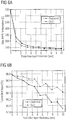
Fig.5 , which shows the two most critical optical properties of different materials, namely the attenuation length and the thermal conductivity, we identify Aluminum as best metal layer (as compared to the normally used Nickel) and Diamond Like Carbon, DLC, as possible heat sink (or alternatively other carbon based ones). - This improved design has been simulated, obtaining, in the case of 1.2um SiC XBPM with 50nm Al contacts, observing a strong decrease of the operating temperature already for thin, 1um, layers (
Fig.6). Fig. 6 (a) depicts the maximal operating temperature and (b) the transmitted beam for a 1.2um SiC XBPM with 50nm Al and different protective layers thicknesses. - Furthermore, the usage of such design and DLC as protective heat sink layer has also other benefits besides the temperature reduction of the XBPM, namely:
- The DLC protects the metal contacts from deterioration.
- The deposition of DLC is cheaper and can be performed on large wafers, as compared to the CVD deposition of Diamond.
- The DLC can be of any type, allowing for very low densities layers, resulting in very high attenuation lengths (
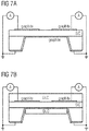
Fig. 5 ) and thus allowing for overall higher XBPM transparencies (seeFig. 7b ). - Finally, in Silicon Carbide is possible to epitaxially grow high quality graphene/graphite layers. Such layers could be used instead of the DLC one not only heat diffusion but also as substitute for metal layers, as this is shown in
Fig.7 (a) or in combination to DLC to achieve even higher transparencies and lower operating temperatures (seeFig.7(b) ). - Embodiments of the present invention will comprise:
- a) A substrate.
- b) An electrically active membrane, i.e. a centrally placed free standing region, being supported by the substrate and wherein the electrically active membrane is substantially made from Silicon Carbide.
- c) A number of electrodes being disposed on the substrate and on the electrically active membrane; each electrode being connected to a separate driving and measuring circuitry, thereby allowing a current to flow upon activation by the x-ray and/or the ion beam through the electrically active membrane.
- d) A heat sink layer that is disposed at least partially on the surface of the electrically active membrane and/or at least partially on the surface of the number of electrodes.
- Preferred embodiments of the present invention may comprise one or more of the following features:
- a) The carbon based layers are made of Diamond like carbon and/or amorphous Carbon and/or graphite.
- b) The carbon based layer is dielectric and used for heat dissipation and as protection layer.
- c) The carbon based layer is conductive and used for heat dissipation and currents flow.
- d) The thickness of the electrically active membrane and the carbon based layer is chosen to allow x-ray beams and/or high energy/high fluxes photons, such as generated by synchrotrons and/or free electron lasers, to go through at least at a level of 80%.
- e) The thickness of the electrically active membrane and the carbon based layer is chosen to allow ion beams, such as generated by cyclotrons, to go through at least at a level of 80%.
- f) The electrically active membrane is built as a thin freestanding layer to achieve high beam transparency, such layer preferably having a thickness in range of a few microns or even in nano-range.
- Preferred embodiment of the present invention are hereinafter described in more detail with reference to the attached drawing that depicts in:
- Figure 1
- A standard XBPM detector comprising a
substrate 2 and an electrically active/transparent membrane 4. A number ofelectrodes substrate 2 and on the electricallyactive membrane 4; saidelectrodes 8 to 12 being connected to a driving andcurrent measuring circuitry 14. - Figure 2
- Overall experimental results on SiC XBPMs.
- Figure 3
- (a) elements composing a full SiC XBPM chip and (b) simulated temperature profiles across the SiC XBMP; Finite element thermal simulations were performed considering the focused pinkbeam setup at the OPTICS beamline at the SWISS LIGHT SOURCE at Paul Scherrer Institute, Villigen, Switzerland (SLS). The considered beamline, in the focused pinkbeam configuration, has a averaged power density of 18kW/cm2, photon energies from 4keV to 20keV with maximum at 10keV and a spot of 100um FWHM.
- Figure 4
- An improved design using DLC or Diamond only as heat sink regions and the thin SiC layer as only electrically active layer.
- Figure 5
- Optical and thermal properties for different materials; properties of Diamond like Carbon (DLC) are strongly dependent on the specific growth, and have been thus averaged.
- Figure 6
- (a) The maximal operating temperature and (b) the transmitted beam for a 1.2um SiC XBPM with 50nm Al and different protective layers
- Figure 7
- (a) An improved design using graphite/graphene layers as heat sink regions and as substitute to metal contacts (b) Combination of graphite/graphene and DLC layers for improved reliability and beam transmission.
-
Figure 1 shows a standard XBPM detector. The standard XBPM detector comprises asubstrate 2 and an electrically active/transparent membrane 4. A number ofelectrodes substrate 2 and on the electricallyactive membrane 4. Saidelectrodes 8 to 12 are connected to a driving and measuringcircuitry 14. -
Fig.4 shows an improved XBPM design which, as compared to the standard design, contains additional layers, here a Diamond likecarbon layer active membrane 4 and/or at least partially on the surface of the number ofelectrodes 8 to 12.Upper DLC layer 18 covers in this embodiment the upper part of the XBPM while alower DLC layer 20 covers the bottom part of the XBPM. This solution allows to take advantage of the superior electrical properties of Silicon Carbide but use the DLC as heat sink, avoiding thermal runaways under high intense beams. -
Fig.5 shows the two most critical optical properties of different materials, namely the attenuation length and the thermal conductivity. Best materials for X-ray beam monitor will show large attenuation length and high thermal conductivities. From it we identify Aluminum as best metal layer (as compared to the normally used Nickel) and Diamond Like Carbon, DLC, as possible best heat sink (or alternatively other carbon based ones). -
Fig.7 (a) shows an alternative design which avoids to use Aluminum as metal contact, using instead graphene/graphite, this will result improved beam transmission.Fig.7(b) shows a combination of graphite/graphene and DLC layers for improved reliability and beam transmission.
Claims (8)
- Photon and/or ion beam position detector (XBPM), comprising:a) a substrate (2);b) an electrically active membrane, i.e. an electrically active free standing region, (4) being supported by the substrate (2), wherein the membrane (4) is substantially made from Silicon Carbide;c) a number of electrodes (8 to 12) being disposed on the substrate (4) and on the electrically active membrane (4); the electrodes (8 to 12) being connected to a measuring circuitry (14), thereby allowing a current to flow upon activation by the x-ray and/or the ion beam through the electrically active membrane (4);d) a carbon based layer (18, 20) that is disposed at least partially on the surface of the electrically active membrane (4) and/or at least partially on the surface of the number of electrodes (8 to 12).
- Photon and/or ion beam detector according to claim 1, wherein the carbon based layers (18, 20) are made of Diamond like carbon and/or amorphous Carbon and/or graphite.
- Photon and/or ion beam detector according to claim 1 or 2, wherein the carbon based layer (18, 20) is dielectric and used for heat dissipation and as protection layer.
- Photon and/or ion beam detector according to claim 1 or 2, wherein the carbon based layer (18, 20) is conductive and used for heat dissipation and currents flow.
- Photon and/or ion beam detector according to claim 1 or 2, wherein the carbon based layer (18, 20) is for some part conductive and used for heat dissipation and currents flow and for some part dielectric and used for heat dissipation and as protection layer.
- Photon and/or ion beam detector according to any of the preceding claims 1 to 4, wherein the thickness of the electrically active membrane (4) and the carbon based layer (18, 20) is chosen to allow beams to go through at least at a level of 60%, preferably at least at a level of 95%.
- Photon and/or ion beam detector according to any of the preceding claims, wherein the electrically active free standing layer (4), built to achieve high beam transparency, has preferably a thickness in range of a few microns or even in nano-range.
- Photon and/or ion beam detector according to any of the preceding claims, wherein the detector, having a multiplicity of electrodes, allows determining not only the beam intensity but also its position (beam monitoring position).
Priority Applications (2)
| Application Number | Priority Date | Filing Date | Title |
|---|---|---|---|
| EP18190666.0A EP3614413A1 (en) | 2018-08-24 | 2018-08-24 | Silicon carbide detectors with improved reliability for photon and/or ion beams |
| PCT/EP2019/071108 WO2020038713A1 (en) | 2018-08-24 | 2019-08-06 | Silicon carbide detectors with improved reliability for photon and/or ion beams |
Applications Claiming Priority (1)
| Application Number | Priority Date | Filing Date | Title |
|---|---|---|---|
| EP18190666.0A EP3614413A1 (en) | 2018-08-24 | 2018-08-24 | Silicon carbide detectors with improved reliability for photon and/or ion beams |
Publications (1)
| Publication Number | Publication Date |
|---|---|
| EP3614413A1 true EP3614413A1 (en) | 2020-02-26 |
Family
ID=63405035
Family Applications (1)
| Application Number | Title | Priority Date | Filing Date |
|---|---|---|---|
| EP18190666.0A Withdrawn EP3614413A1 (en) | 2018-08-24 | 2018-08-24 | Silicon carbide detectors with improved reliability for photon and/or ion beams |
Country Status (2)
| Country | Link |
|---|---|
| EP (1) | EP3614413A1 (en) |
| WO (1) | WO2020038713A1 (en) |
Citations (1)
| Publication number | Priority date | Publication date | Assignee | Title |
|---|---|---|---|---|
| EP1207407A2 (en) * | 1995-04-07 | 2002-05-22 | Rikagaku Kenkyusho | Radiation beam position monitor and position measurement method |
-
2018
- 2018-08-24 EP EP18190666.0A patent/EP3614413A1/en not_active Withdrawn
-
2019
- 2019-08-06 WO PCT/EP2019/071108 patent/WO2020038713A1/en not_active Ceased
Patent Citations (1)
| Publication number | Priority date | Publication date | Assignee | Title |
|---|---|---|---|---|
| EP1207407A2 (en) * | 1995-04-07 | 2002-05-22 | Rikagaku Kenkyusho | Radiation beam position monitor and position measurement method |
Non-Patent Citations (3)
| Title |
|---|
| BERGONZO P ET AL: "Semitransparent CVD diamond detectors for in situ synchrotron radiation beam monitoring", DIAMOND AND RELATED MATERI, ELSEVIER SCIENCE PUBLISHERS, AMSTERDAM, NL, vol. 8, no. 2-5, 1 March 1999 (1999-03-01), pages 920 - 926, XP004365015, ISSN: 0925-9635, DOI: 10.1016/S0925-9635(98)00342-2 * |
| DESJARDINS K ET AL: "Ultra-thin optical grade scCVD diamond as X-ray beam position monitor", JOURNAL OF SYNCHROTRON RADIATION IUCR - INTERNATIONAL UNION OF CRYSTALLOGRAPHY UK, vol. 21, no. 6, 1 November 2014 (2014-11-01), pages 1217 - 1223, XP055551783, ISSN: 0909-0495 * |
| PALLON J ET AL: "Ion beam evaluation of silicon carbide membrane structures intended for particle detectors", NUCLEAR INSTRUMENTS & METHODS IN PHYSICS RESEARCH. SECTION B: BEAM INTERACTIONS WITH MATERIALS AND ATOMS, vol. 371, 30 October 2015 (2015-10-30), pages 132 - 136, XP029462667, ISSN: 0168-583X, DOI: 10.1016/J.NIMB.2015.10.045 * |
Also Published As
| Publication number | Publication date |
|---|---|
| WO2020038713A1 (en) | 2020-02-27 |
Similar Documents
| Publication | Publication Date | Title |
|---|---|---|
| Nida et al. | Silicon carbide X-ray beam position monitors for synchrotron applications | |
| US9281158B2 (en) | X-ray emitting target and X-ray emitting device | |
| US9349891B2 (en) | Submicron gap thermophotovoltaic structure and fabrication method | |
| US20080203397A1 (en) | Switching Device | |
| AU2015346007B2 (en) | Electrical generator system | |
| US7081677B2 (en) | Thermoelectric module | |
| RU2218631C2 (en) | INFRARED RADIATION CONTROLLED CIRCUIT ( VARIANTS ), INFRARED RADIATION DETECTOR AND METHOD OF EMPLOYMENT OF INFRARED RADIATION BASED ON SiC | |
| KR102562059B1 (en) | Thermally insulated electrical contact probe and heated platen assembly | |
| KR20010083046A (en) | Planar electron emitrer (pee) | |
| EP3614413A1 (en) | Silicon carbide detectors with improved reliability for photon and/or ion beams | |
| US20100078558A1 (en) | Infra-red light stimulated cdZnTe spectroscopic semiconductor x-ray and gamma-ray radiation detector | |
| CN110914712B (en) | Radiation detector with built-in depolarization device | |
| EP3719542B1 (en) | Device for non-fully intercepting sensor monitors for ionizing beams | |
| KR101045685B1 (en) | Thermoelectric semiconductor device and its manufacturing method | |
| CN112864005B (en) | Methods for processing semiconductor substrates | |
| US9484474B1 (en) | Ultrananocrystalline diamond contacts for electronic devices | |
| Borges et al. | Testing an indirectly heated cathode ion source: Temperature and thermionic emission | |
| JP2022155345A (en) | Power semiconductor and manufacturing method thereof | |
| US20260004988A1 (en) | X-ray tube with a cooled gate electrode | |
| Lewis et al. | Emission current enhancement from quasi-freestanding epitaxial graphene microstructure electron emitters through surface layered silicon dioxide | |
| US20240047601A1 (en) | Particle detector comprising a porous region made of a semiconductor material, and associated manufacturing method | |
| JP2001358306A (en) | Current limiting device | |
| RU2394306C2 (en) | Device for releasing or absorbing heat | |
| C'TORS | LAWRENCI: RADIATION LABORATORY | |
| Guo et al. | High-temperature Power Electronics: A |
Legal Events
| Date | Code | Title | Description |
|---|---|---|---|
| PUAI | Public reference made under article 153(3) epc to a published international application that has entered the european phase |
Free format text: ORIGINAL CODE: 0009012 |
|
| AK | Designated contracting states |
Kind code of ref document: A1 Designated state(s): AL AT BE BG CH CY CZ DE DK EE ES FI FR GB GR HR HU IE IS IT LI LT LU LV MC MK MT NL NO PL PT RO RS SE SI SK SM TR |
|
| AX | Request for extension of the european patent |
Extension state: BA ME |
|
| STAA | Information on the status of an ep patent application or granted ep patent |
Free format text: STATUS: THE APPLICATION IS DEEMED TO BE WITHDRAWN |
|
| 18D | Application deemed to be withdrawn |
Effective date: 20200827 |