EP3614103B1 - Sensor packages - Google Patents
Sensor packages Download PDFInfo
- Publication number
- EP3614103B1 EP3614103B1 EP19193483.5A EP19193483A EP3614103B1 EP 3614103 B1 EP3614103 B1 EP 3614103B1 EP 19193483 A EP19193483 A EP 19193483A EP 3614103 B1 EP3614103 B1 EP 3614103B1
- Authority
- EP
- European Patent Office
- Prior art keywords
- sensor
- interposer
- package
- external wall
- sensor package
- Prior art date
- Legal status (The legal status is an assumption and is not a legal conclusion. Google has not performed a legal analysis and makes no representation as to the accuracy of the status listed.)
- Active
Links
Images


Classifications
-
- H—ELECTRICITY
- H10—SEMICONDUCTOR DEVICES; ELECTRIC SOLID-STATE DEVICES NOT OTHERWISE PROVIDED FOR
- H10W—GENERIC PACKAGES, INTERCONNECTIONS, CONNECTORS OR OTHER CONSTRUCTIONAL DETAILS OF DEVICES COVERED BY CLASS H10
- H10W72/00—Interconnections or connectors in packages
- H10W72/01—Manufacture or treatment
- H10W72/0198—Manufacture or treatment batch processes
-
- G—PHYSICS
- G01—MEASURING; TESTING
- G01C—MEASURING DISTANCES, LEVELS OR BEARINGS; SURVEYING; NAVIGATION; GYROSCOPIC INSTRUMENTS; PHOTOGRAMMETRY OR VIDEOGRAMMETRY
- G01C19/00—Gyroscopes; Turn-sensitive devices using vibrating masses; Turn-sensitive devices without moving masses; Measuring angular rate using gyroscopic effects
- G01C19/56—Turn-sensitive devices using vibrating masses, e.g. vibratory angular rate sensors based on Coriolis forces
- G01C19/5783—Mountings or housings not specific to any of the devices covered by groups G01C19/5607 - G01C19/5719
-
- B—PERFORMING OPERATIONS; TRANSPORTING
- B81—MICROSTRUCTURAL TECHNOLOGY
- B81B—MICROSTRUCTURAL DEVICES OR SYSTEMS, e.g. MICROMECHANICAL DEVICES
- B81B7/00—Microstructural systems ; Auxiliary parts of microstructural devices or systems
- B81B7/0032—Packages or encapsulation
- B81B7/0058—Packages or encapsulation for protecting against damages due to external chemical or mechanical influences, e.g. shocks or vibrations
-
- B—PERFORMING OPERATIONS; TRANSPORTING
- B81—MICROSTRUCTURAL TECHNOLOGY
- B81B—MICROSTRUCTURAL DEVICES OR SYSTEMS, e.g. MICROMECHANICAL DEVICES
- B81B7/00—Microstructural systems ; Auxiliary parts of microstructural devices or systems
- B81B7/0032—Packages or encapsulation
- B81B7/007—Interconnections between the MEMS and external electrical signals
-
- B—PERFORMING OPERATIONS; TRANSPORTING
- B81—MICROSTRUCTURAL TECHNOLOGY
- B81C—PROCESSES OR APPARATUS SPECIALLY ADAPTED FOR THE MANUFACTURE OR TREATMENT OF MICROSTRUCTURAL DEVICES OR SYSTEMS
- B81C1/00—Manufacture or treatment of devices or systems in or on a substrate
- B81C1/00015—Manufacture or treatment of devices or systems in or on a substrate for manufacturing microsystems
- B81C1/00261—Processes for packaging MEMS devices
- B81C1/00301—Connecting electric signal lines from the MEMS device with external electrical signal lines, e.g. through vias
-
- G—PHYSICS
- G01—MEASURING; TESTING
- G01L—MEASURING FORCE, STRESS, TORQUE, WORK, MECHANICAL POWER, MECHANICAL EFFICIENCY, OR FLUID PRESSURE
- G01L19/00—Details of, or accessories for, apparatus for measuring steady or quasi-steady pressure of a fluent medium insofar as such details or accessories are not special to particular types of pressure gauges
- G01L19/0061—Electrical connection means
- G01L19/0069—Electrical connection means from the sensor to its support
-
- G—PHYSICS
- G01—MEASURING; TESTING
- G01L—MEASURING FORCE, STRESS, TORQUE, WORK, MECHANICAL POWER, MECHANICAL EFFICIENCY, OR FLUID PRESSURE
- G01L19/00—Details of, or accessories for, apparatus for measuring steady or quasi-steady pressure of a fluent medium insofar as such details or accessories are not special to particular types of pressure gauges
- G01L19/0061—Electrical connection means
- G01L19/0084—Electrical connection means to the outside of the housing
-
- G—PHYSICS
- G01—MEASURING; TESTING
- G01L—MEASURING FORCE, STRESS, TORQUE, WORK, MECHANICAL POWER, MECHANICAL EFFICIENCY, OR FLUID PRESSURE
- G01L19/00—Details of, or accessories for, apparatus for measuring steady or quasi-steady pressure of a fluent medium insofar as such details or accessories are not special to particular types of pressure gauges
- G01L19/06—Means for preventing overload or deleterious influence of the measured medium on the measuring device or vice versa
- G01L19/0627—Protection against aggressive medium in general
- G01L19/0645—Protection against aggressive medium in general using isolation membranes, specially adapted for protection
-
- G—PHYSICS
- G01—MEASURING; TESTING
- G01P—MEASURING LINEAR OR ANGULAR SPEED, ACCELERATION, DECELERATION, OR SHOCK; INDICATING PRESENCE, ABSENCE, OR DIRECTION, OF MOVEMENT
- G01P1/00—Details of instruments
- G01P1/02—Housings
- G01P1/023—Housings for acceleration measuring devices
-
- H—ELECTRICITY
- H10—SEMICONDUCTOR DEVICES; ELECTRIC SOLID-STATE DEVICES NOT OTHERWISE PROVIDED FOR
- H10W—GENERIC PACKAGES, INTERCONNECTIONS, CONNECTORS OR OTHER CONSTRUCTIONAL DETAILS OF DEVICES COVERED BY CLASS H10
- H10W72/00—Interconnections or connectors in packages
- H10W72/50—Bond wires
-
- H—ELECTRICITY
- H10—SEMICONDUCTOR DEVICES; ELECTRIC SOLID-STATE DEVICES NOT OTHERWISE PROVIDED FOR
- H10W—GENERIC PACKAGES, INTERCONNECTIONS, CONNECTORS OR OTHER CONSTRUCTIONAL DETAILS OF DEVICES COVERED BY CLASS H10
- H10W74/00—Encapsulations, e.g. protective coatings
- H10W74/10—Encapsulations, e.g. protective coatings characterised by their shape or disposition
-
- B—PERFORMING OPERATIONS; TRANSPORTING
- B81—MICROSTRUCTURAL TECHNOLOGY
- B81B—MICROSTRUCTURAL DEVICES OR SYSTEMS, e.g. MICROMECHANICAL DEVICES
- B81B2207/00—Microstructural systems or auxiliary parts thereof
- B81B2207/07—Interconnects
Definitions
- the present disclosure relates to the packaging of sensors, and maximising sensor package resilience under high stress. There is disclosed a sensor package and methods of making a sensor package.
- Sensors for example pressure sensors or inertial sensors (such as accelerometers and gyroscopes) are used in many applications, including inertial navigation, robotics, avionics, and automobiles. In inertial navigation applications, such sensors may be found in self-contained systems known as "inertial measurement units" (IMUs). IMUs typically contain a plurality of accelerometers and/or gyroscopes, and provide an estimate of an object's travel parameters such as angular rate, acceleration, altitude, position, attitude and velocity, based on the outputs of gyroscope(s) and/or accelerometer(s). Each inertial sensor in an IMU is a self-contained package.
- IMUs inertial measurement units
- US2014/072151 describes a microphone package comprising a MEMS microphone mounted on a substrate and sealed within a cavity using a thermoplastic lid, connected by conductive trace to an electrical component mounted on the thermoplastic lid.
- US9932221 describes a multi-layered packaged semiconductor device having fluidically sealable and fluidically exposed compartments.
- US2006/130582 describes a resin-sealed semiconductor device comprising a semiconductor chip mounted on a chip mounting section of a lead frame.
- US2003/177831 describes a dynamic sensor such as an acceleration sensor comprising a sensor chip and a circuit chip mounted within a common package, in which a mounting surface and an adhesive film are used to reduce thermal stress transfer to the circuit chip.
- Microelectromechanical systems (MEMS)-based sensors can be used e.g. to measure pressure or temperature, or linear or angular motion without a fixed point of reference.
- MEMS pressure sensors often work on the principle of mechanical deformation of a MEMS structure due to fluid pressure.
- MEMS gyroscopes, or strictly speaking MEMS angular rate sensors can measure angular rate by observing the response of a vibrating MEMS structure to Coriolis force.
- MEMS accelerometers can measure linear acceleration by observing the response of a proof mass suspended on a spring in a MEMS structure.
- High performance MEMS inertial sensors are defined by their bias and scale factor stability.
- the sensors may on occasion be subject to extremely high forces e.g. accelerations on the order of >20,000G. Under such conditions, components within the sensor package may begin to fail.
- the first failure within the sensor package occurs due to the wire bonds connecting the package to the sensor.
- the wire bonds may short circuit one another, or experience a joint break at the place where the wire bond is joined to the pad of the sensor or package. This is obviously undesirable as it decreases the functional range of the sensor, and furthermore requires replacement of the unit in either breakage scenario described above.
- the present disclosure seeks to address at least some of these shortcomings.
- the present disclosure relates to a sensor package and a method of making a sensor package. It will be appreciated that using an interposer, wire bonded to both the sensor and the at least one external wall, is an improved approach to electrically connecting a sensor and a sensor package as compared to the prior art.
- the interposer allows for short wire bonds from the sensor and the at least one external wall to the interposer, replacing the single, long wire bond from the sensor to the at least one external wall in the prior art. This provides improved resilience of the sensor package under high stress. Furthermore, it allows an existing sensor and package combination to be improved without needing to redesign either component.
- a sensor package and a method of making a sensor package are described in further detail below.
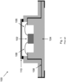
- Fig. 1 shows a cross sectional schematic of a prior art sensor package assembly 100.
- the sensor package comprises a sensor 102, package 104, wire bonds 106, conductive tracking 108, and a lid 110.
- the sensor 102 In order to protect a sensor 102 from external influences that may damage or destroy it when in use, the sensor 102 is placed in a protective package 104 that surrounds the sensor 102.
- the sensor 102 after being placed in the package 104, is wire bonded to the package 104, in order for electrical connections to be made from the sensor 102 to the external world.
- the protective package 104 comprises conductive tracking 108 which allows an electrical connection to be made from outside the package 104 to the sensor 102.
- a lid 110 is bonded to the package 104. This sealing of the internal space in the package 104 prevents any external influence directly affecting the sensor 102.
- the first failure within the sensor package assembly 100 due to such high stress events is a failure of one or more wire bonds 106.
- the failure of a wire bond 106 may occur as a short circuit of one wire bond 106 to another, or the entire wire bond 106 may collapse.
- a collapse may occur as a joint failure, i.e. where the wire bond 106 is joined to the sensor 102 or the metal tracking 108.
- Fig. 2 shows a cross sectional schematic of a sensor package 200 in accordance with an example of the present disclosure.
- the sensor package 200 comprises a sensor 202, a base 204, an interposer 206, wire bonds 208, conductive tracking 210, 212, a lid 214, sealed to the external walls 213 and optional adhesive 216 between the interposer 206 and the external walls 213.
- an interposer 206 is inserted between the sensor 202 and the external walls 213, resting on the package base 204.
- Conductive tracking 210 is deposited on the interposer 206 before it is added to the sensor package 200 to allow an electrical connection to be made from one side of the interposer 206 to the other.
- the sensor 202 can then be wire bonded 208 to the conductive tracking 210 of the interposer 206, and the conductive tracking 210 of the interposer 206 can be wire bonded 208 to the conductive tracking 212 on the external walls 213. This creates an electrical connection from the sensor 202 to the outside of the package 200, via the interposer 206.
- the present inventors have discovered that the failure rate of a wire bond 208 is correlated to the weight of the wire bond 208, and therefore its length. Whilst it is envisaged that other changes such as reducing wire bond 208 diameter or changing the wire bond 208 material may also affect the wire bond 208 weight, the present disclosure is focused on wire bond 208 length, as this approach also provides other effects explained in more detail below.
- the insertion and fit of the interposer 206 in this example allows for extremely short wire bonds 208 within the package 204, whilst maintaining the electrical connection between the sensor 202 and the conductive tracking 212 on the package 204.
- These short wire bonds 208 are significantly more resilient to high stresses than the long wire bonds 106 of Fig. 1 . This allows the sensor package 200 to be more resilient to shocks and/or damage, and maintain an increased operating range.
- an interposer 206 allows use of a pre-existing package 204 design, together with the pre-existing package 204 manufacturing method.
- the interposer 206 can be retrofitted into such packages 204, removing the need to redesign the entire package 204 to achieve the same reduced wire bond 208 length.
- the interposer 206 is adhesively bonded to the package 204 by an adhesive layer 216. This may increase the resilience of the sensor package 200 by ensuring that the interposer 206 stays in place under high stress.
- Figs. 3a and 3b show perspective views of an interposer 300, and a sensor package 310, respectively, in accordance with examples of the present disclosure.
- Fig. 3a shows an interposer 300 in accordance with an example of the present disclosure.
- the interposer 300 is patterned with conductive tracking 302, which allow for connections, for example wire bonds, to be made to it.
- the interposer 300 comprises cut-outs 304 which allow adhesive to be dispensed without the adhesive coming into contact with the conductive tracking 302. This prevents any potential contamination of the conductive tracking 302, which could further prevent any potential wire bonding process from taking place.
- the adhesive also bonds the interposer 300 to one or more externals walls of a package, increasing the resilience of a sensor package , as mentioned above.
- Fig. 3b shows a sensor package 310 in accordance with an example of the present disclosure.
- the sensor package 310 comprises the interposer 300 of Fig. 3a fitted inside its external walls 313 and a sensor 316 fitted inside or surrounded by the interposer 300.
- the package 310 is of a pre-existing, mass produced design, and so the interposer 300 is designed to fit specifically within the package 310. As mentioned above, this avoids a redesign of the package 310.
- the interposer 300 is inserted into the package 310, surrounding the sensor 316, occupying the majority of the space between the sensor 316 and the package 310. It can be seen how the interposer 300 is shaped to fit the geometry defined by the external walls 313 of the package 310 and sits in contact with the external walls 313 at least in the corners of the square geometry in this example.
- Adhesive may be dispensed into the cut-outs 304 as described above to secure the interposer 300 in place within the package 310.
- the cut-outs 304 prevent the interposer 300 from moving up past the cured adhesive, which increases the resilience of the sensor package 310.
- the sensor 316 is wire bonded 318 to the conductive tracking 302 on the interposer 300.
- the conductive tracking 302 on the interposer 300 is further wire bonded 320 to the conductive tracking 314 carried by the external walls 313 of the package 310. As described above, this enables an electrical connection to be made between the sensor 316 and the package 310.
- the decreased length of the wire bonds 318, 320 increases the resilience of the sensor package 310 under high stress.
- a sensor package may facilitate wire bonds of a decreased length.
- the present inventors have realised that a decreased wire bond length corresponds to a reduced chance of breakage under high stresses.
- the interposer is disposed in the space between the external wall and the sensor, the wire bonds typically joining the sensor directly to the external wall can be shortened into two wire bonds between the sensor and the interposer, and the interposer and the external wall.
- These shortened wire bonds may be less susceptible to high g-force impacts or shocks, increasing the resilience and operating range of the sensor package.
- the present inventors have realised that there is a correlation between the weight of a wire bond, and its susceptibility to breaking under high stress.
- Use of the present disclosure may further enable the use of a pre-existing package design, together with a pre-existing package manufacturing method.
- the interposer can be retrofitted into such pre-existing packages, without any need to redesign an entire package. This saves both the costs and time of such a redesign.
- Use of the present disclosure may also allow for existing sensors to be used in emerging markets that require extreme robustness, where such devices may not previously have been suitable.
- the interposer comprises conductive tracking, the sensor is wired bonded to the conductive tracking, and the conductive tracking is wire bonded to the at least one external wall. This may allow the sensor to be electrically connected to the at least one external wall, via the conductive tracking of the interposer. This may allow signals from the sensor to be accessed from outside the package. This may also allow for further reduction in the length of the wire bonds, as the conductive tracking may span the width of the interposer. The wire bonds may then be joined to the interposer at the edges. Furthermore, the tracking may be designed to optimise the distance between where a connection is made from the sensor and where a connection is made from the interposer. The tracking may also be designed to optimise the distance between where a connection is made from the package and where a connection is made from the interposer.
- the first or second material is ceramic, for example alumina.
- the second material is plastic.
- the second material is FR-4.
- the interposer is formed by injection moulding. This may allow for existing manufacturing techniques to be utilised, for example Moulded Interconnect Device technology, streamlining manufacture and reducing costs.
- the interposer is a Moulded Interconnect Device (MID).
- the interposer is in contact with the at least one external wall.
- the interposer may be in physical contact with the at least one external wall as well as being wire bonded to the at least one external wall for electrical contact.
- This physical contact of the interposer and the at least one external wall may increase the robustness of the package, by reducing the chance of the interposer moving or becoming misaligned within the sensor package during use.
- the interposer may be fitted inside the package in contact with the at least one external wall.
- the interposer is shaped to fit the geometry defined by the at least one external wall.
- the sensor package comprises at least four external walls forming a square, rectangular or polygonal geometry.
- the interposer may be shaped to have a corresponding square, rectangular or polygonal geometry such that the interposer fits inside the package at least partially in contact with the at least four external walls.
- the interposer is preferably in contact with the external walls at least in the corners of the square, rectangular or polygonal geometry.
- the interposer is adhesively bonded to the at least one external wall. This adhesion may further improve the stability and resilience of the sensor package under stress.
- the interposer is shaped to accommodate the adhesive used to adhesively bonded the interposer to the at least one external wall.
- the interposer may comprise cut-outs which are shaped to accommodate the adhesive.
- the adhesive accommodated by the cut-outs may increase the resilience of the sensor package under stress.
- the cut-outs may be arranged between areas of contact, for example between the corners. In such examples the sensor package can benefit from a robust fit with the interposer and the bonding provided by the adhesive.
- At least two of the interposer, the sensor, and the at least one external wall are in the same plane. This may allow for a further reduced wire bond length between the sensor and the interposer. This may also allow for a further reduced wire bond length between the interposer and the at least one external wall. In some examples, the interposer, the external wall and the sensor will all be in the same plane.
- the interposer surrounds the sensor. This may allow for decreased length wire bonds to be made between the interposer and the sensor.
- the at least one external wall surrounds the interposer. This may allow for decreased length wire bonds to be made between the at least one external wall and the interposer.
- the interposer fills at least 50% of the space between the sensor and the at least one external wall. This may allow a decreased length wire bond to connect the interposer and the sensor, and/or the interposer and the at least one external wall. In some examples the interposer fills at least 75% of the space between the sensor and the at least one external wall.
- the senor is a MEMS sensor.
- the MEMS sensor is silicon-based.
- the MEMS sensor is an inertial sensor.
- the MEMS sensor is an accelerometer, a gyroscope, or a pressure sensor.
- the sensor package further comprises potting or a lid to seal the package.
- the interposer does not seal the package.
- the sealing of the sensor package by potting or a lid may protect the sensor from any direct external influences that may damage or destroy the sensor. Sealing of the sensor package further allows control of the internal environment of the package, which may be optimised depending on the sensor.
- the method mentioned above further comprises: arranging at least two of the interposer, the sensor, and the at least one external wall in the same plane.
- the method mentioned above further comprises: adhesively bonding the interposer to the at least one external wall.
Landscapes
- Engineering & Computer Science (AREA)
- Microelectronics & Electronic Packaging (AREA)
- General Physics & Mathematics (AREA)
- Physics & Mathematics (AREA)
- Manufacturing & Machinery (AREA)
- Computer Hardware Design (AREA)
- Toxicology (AREA)
- General Health & Medical Sciences (AREA)
- Health & Medical Sciences (AREA)
- Chemical & Material Sciences (AREA)
- Analytical Chemistry (AREA)
- Radar, Positioning & Navigation (AREA)
- Remote Sensing (AREA)
- Pressure Sensors (AREA)
- Measuring Fluid Pressure (AREA)
- Gyroscopes (AREA)
Description
- The present disclosure relates to the packaging of sensors, and maximising sensor package resilience under high stress. There is disclosed a sensor package and methods of making a sensor package.
- Sensors, for example pressure sensors or inertial sensors (such as accelerometers and gyroscopes) are used in many applications, including inertial navigation, robotics, avionics, and automobiles. In inertial navigation applications, such sensors may be found in self-contained systems known as "inertial measurement units" (IMUs). IMUs typically contain a plurality of accelerometers and/or gyroscopes, and provide an estimate of an object's travel parameters such as angular rate, acceleration, altitude, position, attitude and velocity, based on the outputs of gyroscope(s) and/or accelerometer(s). Each inertial sensor in an IMU is a self-contained package.
US2014/072151 describes a microphone package comprising a MEMS microphone mounted on a substrate and sealed within a cavity using a thermoplastic lid, connected by conductive trace to an electrical component mounted on the thermoplastic lid.US9932221 US2006/130582 describes a resin-sealed semiconductor device comprising a semiconductor chip mounted on a chip mounting section of a lead frame.US2003/177831 describes a dynamic sensor such as an acceleration sensor comprising a sensor chip and a circuit chip mounted within a common package, in which a mounting surface and an adhesive film are used to reduce thermal stress transfer to the circuit chip. - Microelectromechanical systems (MEMS)-based sensors can be used e.g. to measure pressure or temperature, or linear or angular motion without a fixed point of reference. MEMS pressure sensors often work on the principle of mechanical deformation of a MEMS structure due to fluid pressure. MEMS gyroscopes, or strictly speaking MEMS angular rate sensors, can measure angular rate by observing the response of a vibrating MEMS structure to Coriolis force. MEMS accelerometers can measure linear acceleration by observing the response of a proof mass suspended on a spring in a MEMS structure. High performance MEMS inertial sensors are defined by their bias and scale factor stability.
- Due to the applications of such sensors, they may on occasion be subject to extremely high forces e.g. accelerations on the order of >20,000G. Under such conditions, components within the sensor package may begin to fail. Typically, the first failure within the sensor package occurs due to the wire bonds connecting the package to the sensor. The wire bonds may short circuit one another, or experience a joint break at the place where the wire bond is joined to the pad of the sensor or package. This is obviously undesirable as it decreases the functional range of the sensor, and furthermore requires replacement of the unit in either breakage scenario described above.
- The present disclosure seeks to address at least some of these shortcomings.
- According to a first aspect of this disclosure, there is provided a sensor package according to claim 1.
- According to a second aspect of this disclosure, there is provided a method of making a sensor package according to claim 10
-
-
Fig. 1 shows a cross sectional schematic of a prior art sensor package. -
Fig. 2 shows a cross sectional schematic of a sensor package in accordance with an example of the present disclosure. -
Figs. 3a and 3b show perspective views of an interposer, and a sensor package, respectively, in accordance with examples of the present disclosure. - The present disclosure relates to a sensor package and a method of making a sensor package. It will be appreciated that using an interposer, wire bonded to both the sensor and the at least one external wall, is an improved approach to electrically connecting a sensor and a sensor package as compared to the prior art. The interposer allows for short wire bonds from the sensor and the at least one external wall to the interposer, replacing the single, long wire bond from the sensor to the at least one external wall in the prior art. This provides improved resilience of the sensor package under high stress. Furthermore, it allows an existing sensor and package combination to be improved without needing to redesign either component.
- Some non-limiting examples of a sensor package and a method of making a sensor package are described in further detail below.
-
Fig. 1 shows a cross sectional schematic of a prior artsensor package assembly 100. The sensor package comprises asensor 102,package 104,wire bonds 106,conductive tracking 108, and alid 110. - In order to protect a
sensor 102 from external influences that may damage or destroy it when in use, thesensor 102 is placed in aprotective package 104 that surrounds thesensor 102. Thesensor 102, after being placed in thepackage 104, is wire bonded to thepackage 104, in order for electrical connections to be made from thesensor 102 to the external world. Theprotective package 104 comprisesconductive tracking 108 which allows an electrical connection to be made from outside thepackage 104 to thesensor 102. In order to fully seal thepackage 104 from external influences, alid 110 is bonded to thepackage 104. This sealing of the internal space in thepackage 104 prevents any external influence directly affecting thesensor 102. - However, extremely stressful events, for example very high accelerations, may cause failures or malfunctions within the
sensor package assembly 100. Typically, the first failure within thesensor package assembly 100 due to such high stress events is a failure of one ormore wire bonds 106. The failure of awire bond 106 may occur as a short circuit of onewire bond 106 to another, or theentire wire bond 106 may collapse. A collapse may occur as a joint failure, i.e. where thewire bond 106 is joined to thesensor 102 or themetal tracking 108. -
Fig. 2 shows a cross sectional schematic of asensor package 200 in accordance with an example of the present disclosure. Thesensor package 200 comprises asensor 202, abase 204, aninterposer 206,wire bonds 208,conductive tracking lid 214, sealed to theexternal walls 213 andoptional adhesive 216 between theinterposer 206 and theexternal walls 213. - In this example, an
interposer 206 is inserted between thesensor 202 and theexternal walls 213, resting on thepackage base 204.Conductive tracking 210 is deposited on theinterposer 206 before it is added to thesensor package 200 to allow an electrical connection to be made from one side of theinterposer 206 to the other. Thesensor 202 can then be wire bonded 208 to theconductive tracking 210 of theinterposer 206, and theconductive tracking 210 of theinterposer 206 can be wire bonded 208 to theconductive tracking 212 on theexternal walls 213. This creates an electrical connection from thesensor 202 to the outside of thepackage 200, via theinterposer 206. - The present inventors have discovered that the failure rate of a
wire bond 208 is correlated to the weight of thewire bond 208, and therefore its length. Whilst it is envisaged that other changes such as reducingwire bond 208 diameter or changing thewire bond 208 material may also affect thewire bond 208 weight, the present disclosure is focused onwire bond 208 length, as this approach also provides other effects explained in more detail below. - The insertion and fit of the
interposer 206 in this example allows for extremelyshort wire bonds 208 within thepackage 204, whilst maintaining the electrical connection between thesensor 202 and theconductive tracking 212 on thepackage 204. Theseshort wire bonds 208 are significantly more resilient to high stresses than thelong wire bonds 106 ofFig. 1 . This allows thesensor package 200 to be more resilient to shocks and/or damage, and maintain an increased operating range. - Furthermore, the addition of an
interposer 206 allows use of apre-existing package 204 design, together with thepre-existing package 204 manufacturing method. Thus, theinterposer 206 can be retrofitted intosuch packages 204, removing the need to redesign theentire package 204 to achieve the same reducedwire bond 208 length. In this example theinterposer 206 is adhesively bonded to thepackage 204 by anadhesive layer 216. This may increase the resilience of thesensor package 200 by ensuring that theinterposer 206 stays in place under high stress. -
Figs. 3a and 3b show perspective views of aninterposer 300, and asensor package 310, respectively, in accordance with examples of the present disclosure. -
Fig. 3a shows aninterposer 300 in accordance with an example of the present disclosure. Theinterposer 300 is patterned withconductive tracking 302, which allow for connections, for example wire bonds, to be made to it. As shown, theinterposer 300 comprises cut-outs 304 which allow adhesive to be dispensed without the adhesive coming into contact with theconductive tracking 302. This prevents any potential contamination of theconductive tracking 302, which could further prevent any potential wire bonding process from taking place. The adhesive also bonds theinterposer 300 to one or more externals walls of a package, increasing the resilience of a sensor package , as mentioned above. -
Fig. 3b shows asensor package 310 in accordance with an example of the present disclosure. Thesensor package 310 comprises theinterposer 300 ofFig. 3a fitted inside itsexternal walls 313 and asensor 316 fitted inside or surrounded by theinterposer 300. - The
package 310 is of a pre-existing, mass produced design, and so theinterposer 300 is designed to fit specifically within thepackage 310. As mentioned above, this avoids a redesign of thepackage 310. - As shown, the
interposer 300 is inserted into thepackage 310, surrounding thesensor 316, occupying the majority of the space between thesensor 316 and thepackage 310. It can be seen how theinterposer 300 is shaped to fit the geometry defined by theexternal walls 313 of thepackage 310 and sits in contact with theexternal walls 313 at least in the corners of the square geometry in this example. - Adhesive may be dispensed into the cut-
outs 304 as described above to secure theinterposer 300 in place within thepackage 310. The cut-outs 304 prevent theinterposer 300 from moving up past the cured adhesive, which increases the resilience of thesensor package 310. - As shown, the
sensor 316 is wire bonded 318 to theconductive tracking 302 on theinterposer 300. Theconductive tracking 302 on theinterposer 300 is further wire bonded 320 to theconductive tracking 314 carried by theexternal walls 313 of thepackage 310. As described above, this enables an electrical connection to be made between thesensor 316 and thepackage 310. As previously mentioned, the decreased length of thewire bonds sensor package 310 under high stress. - Thus it will be seen that, in accordance with the present disclosure, a sensor package is provided that may facilitate wire bonds of a decreased length. The present inventors have realised that a decreased wire bond length corresponds to a reduced chance of breakage under high stresses. As the interposer is disposed in the space between the external wall and the sensor, the wire bonds typically joining the sensor directly to the external wall can be shortened into two wire bonds between the sensor and the interposer, and the interposer and the external wall. These shortened wire bonds may be less susceptible to high g-force impacts or shocks, increasing the resilience and operating range of the sensor package. The present inventors have realised that there is a correlation between the weight of a wire bond, and its susceptibility to breaking under high stress. Thus, by reducing the length of a wire bond, its weight is also decreased, and therefore its chance of breakage under high stress. Whilst it is envisaged that other changes such as reducing wire bond diameter or changing the wire bond material may also affect the wire bond weight, the present disclosure is focused on wire bond length.
- Use of the present disclosure may further enable the use of a pre-existing package design, together with a pre-existing package manufacturing method. Thus, the interposer can be retrofitted into such pre-existing packages, without any need to redesign an entire package. This saves both the costs and time of such a redesign.
- Use of the present disclosure may also allow for existing sensors to be used in emerging markets that require extreme robustness, where such devices may not previously have been suitable.
- The interposer comprises conductive tracking, the sensor is wired bonded to the conductive tracking, and the conductive tracking is wire bonded to the at least one external wall. This may allow the sensor to be electrically connected to the at least one external wall, via the conductive tracking of the interposer. This may allow signals from the sensor to be accessed from outside the package. This may also allow for further reduction in the length of the wire bonds, as the conductive tracking may span the width of the interposer. The wire bonds may then be joined to the interposer at the edges. Furthermore, the tracking may be designed to optimise the distance between where a connection is made from the sensor and where a connection is made from the interposer. The tracking may also be designed to optimise the distance between where a connection is made from the package and where a connection is made from the interposer.
- In some examples, the first or second material is ceramic, for example alumina. In some examples, the second material is plastic. In some examples, the second material is FR-4.
- According to one or more examples of the present disclosure, in addition or alternatively, the interposer is formed by injection moulding. This may allow for existing manufacturing techniques to be utilised, for example Moulded Interconnect Device technology, streamlining manufacture and reducing costs. In some examples, the interposer is a Moulded Interconnect Device (MID).
- According to one or more examples of the present disclosure, in addition or alternatively, the interposer is in contact with the at least one external wall. This means that the interposer may be in physical contact with the at least one external wall as well as being wire bonded to the at least one external wall for electrical contact. This physical contact of the interposer and the at least one external wall may increase the robustness of the package, by reducing the chance of the interposer moving or becoming misaligned within the sensor package during use. For example, the interposer may be fitted inside the package in contact with the at least one external wall. Preferably, the interposer is shaped to fit the geometry defined by the at least one external wall. In some examples, the sensor package comprises at least four external walls forming a square, rectangular or polygonal geometry. In such examples, the interposer may be shaped to have a corresponding square, rectangular or polygonal geometry such that the interposer fits inside the package at least partially in contact with the at least four external walls. In such examples, the interposer is preferably in contact with the external walls at least in the corners of the square, rectangular or polygonal geometry.
- According to one or more examples of the present disclosure, in addition or alternatively, the interposer is adhesively bonded to the at least one external wall. This adhesion may further improve the stability and resilience of the sensor package under stress.
- According to one or more examples of the present disclosure, in addition or alternatively, the interposer is shaped to accommodate the adhesive used to adhesively bonded the interposer to the at least one external wall. In some examples, the interposer may comprise cut-outs which are shaped to accommodate the adhesive. In some examples, the adhesive accommodated by the cut-outs may increase the resilience of the sensor package under stress. In those examples wherein the interposer is fitted inside the package in contact with the at least one external wall, for example fitted in contact with the corners defined by the external walls, the cut-outs may be arranged between areas of contact, for example between the corners. In such examples the sensor package can benefit from a robust fit with the interposer and the bonding provided by the adhesive.
- According to one or more examples of the present disclosure, in addition or alternatively, at least two of the interposer, the sensor, and the at least one external wall are in the same plane. This may allow for a further reduced wire bond length between the sensor and the interposer. This may also allow for a further reduced wire bond length between the interposer and the at least one external wall. In some examples, the interposer, the external wall and the sensor will all be in the same plane.
- According to one or more examples of the present disclosure, in addition or alternatively, the interposer surrounds the sensor. This may allow for decreased length wire bonds to be made between the interposer and the sensor. In some examples, the at least one external wall surrounds the interposer. This may allow for decreased length wire bonds to be made between the at least one external wall and the interposer.
- According to one or more examples of the present disclosure, in addition or alternatively, the interposer fills at least 50% of the space between the sensor and the at least one external wall. This may allow a decreased length wire bond to connect the interposer and the sensor, and/or the interposer and the at least one external wall. In some examples the interposer fills at least 75% of the space between the sensor and the at least one external wall.
- According to one or more examples of the present disclosure, in addition or alternatively, the sensor is a MEMS sensor. In some examples, the MEMS sensor is silicon-based. In some examples, the MEMS sensor is an inertial sensor. In some examples, the MEMS sensor is an accelerometer, a gyroscope, or a pressure sensor.
- According to one or more examples of the present disclosure, the sensor package further comprises potting or a lid to seal the package. In this way, the interposer does not seal the package. The sealing of the sensor package by potting or a lid may protect the sensor from any direct external influences that may damage or destroy the sensor. Sealing of the sensor package further allows control of the internal environment of the package, which may be optimised depending on the sensor.
- In one or more examples the method mentioned above further comprises: arranging at least two of the interposer, the sensor, and the at least one external wall in the same plane.
- In one or more examples the method mentioned above further comprises: adhesively bonding the interposer to the at least one external wall.
- It will be appreciated by those skilled in the art that the present disclosure has been illustrated by describing one or more specific examples thereof, but is not limited to these examples; many variations and modifications are possible, within the scope of the accompanying claims. Features of any aspect or example described herein may, wherever appropriate, be applied to any other aspect or example described herein.
- Where reference is made to different examples or sets of examples, it should be understood that these are not necessarily distinct but may overlap.
Claims (12)
- A sensor package (200; 310) comprising:a sensor (202; 316);at least one external wall (213; 313);an interposer (206; 300), arranged between the sensor (202; 316) and the at least one external wall (213; 313);wherein the interposer (206; 300) comprises conductive tracking (210; 302);wherein the sensor (202; 316) is wire bonded (208; 318) to the conductive tracking (210; 302);wherein the at least one external wall (213; 313) is made from a first material, the interposer (206; 300) is made from a second material, and the first and second materials are different; characterized in thatthe conductive tracking (210; 302) is wire bonded (208; 320) to the at least one external wall (213; 313) and in thatthe second material is plastic.
- The sensor package (200; 310) of claim 1, wherein the interposer (206; 300) is formed by injection moulding.
- The sensor package (200; 310) of claim 1 or 2, wherein the interposer (206; 300) is a Moulded Interconnect Device (MID).
- The sensor package (200; 310) of any preceding claim, wherein the interposer (206; 300) is fitted inside the package (200; 310) in contact with the at least one external wall (213; 313).
- The sensor package (200; 310) of any preceding claim, wherein the interposer (206; 300) is adhesively bonded to the at least one external wall (213; 313).
- The sensor package (200; 310) of claim 5, wherein the interposer (206; 300) is shaped to accommodate the adhesive.
- The sensor package (200; 310) of any preceding claim, wherein at least two of the interposer (206; 300), the sensor (202; 316), and the at least one external wall (213; 313) are in the same plane.
- The sensor package (200; 310) of any preceding claim, wherein the interposer (206; 300) fills at least 50% of the space between the sensor (202; 316) and the at least one external wall (213; 313).
- The sensor package (200; 310) of any preceding claim, wherein the sensor package (200; 310) further comprises potting or a lid to seal the package (200; 310).
- A method of making a sensor package (200; 310), the sensor package (200; 310) comprising:a sensor (202; 316); andat least one external wall (213; 313);wherein the method comprises:inserting an interposer (206; 300) comprising conductive tracking (210; 302) into the sensor package (200; 310) between the sensor (202; 316) and the at least one external wall (213; 313);wire bonding (208; 318) the sensor (202; 316) to the conductive tracking (210; 302);wherein the at least one external wall (213; 313) is made from a first material, the interposer (206; 300) is made from a second material, and the first and second materials are different; characterized in thatthe method further comprises wire bonding (208;320) the conductive tracking (210;302) to the at least one external wall (213;313)and in that the second material is plastic.
- The method of claim 10, further comprising:
arranging at least two of the interposer (206; 300), the sensor (202; 316), and the at least one external wall (213; 313) in the same plane. - The method of claim 10 or 11, further comprising:
adhesively bonding the interposer (206; 300) to the at least one external wall (213; 313).
Applications Claiming Priority (1)
| Application Number | Priority Date | Filing Date | Title |
|---|---|---|---|
| GB1813815.6A GB2582238A (en) | 2018-08-24 | 2018-08-24 | Sensor packages |
Publications (2)
| Publication Number | Publication Date |
|---|---|
| EP3614103A1 EP3614103A1 (en) | 2020-02-26 |
| EP3614103B1 true EP3614103B1 (en) | 2025-01-08 |
Family
ID=63715279
Family Applications (1)
| Application Number | Title | Priority Date | Filing Date |
|---|---|---|---|
| EP19193483.5A Active EP3614103B1 (en) | 2018-08-24 | 2019-08-23 | Sensor packages |
Country Status (5)
| Country | Link |
|---|---|
| US (1) | US11401158B2 (en) |
| EP (1) | EP3614103B1 (en) |
| JP (1) | JP7616820B2 (en) |
| KR (1) | KR102719250B1 (en) |
| GB (1) | GB2582238A (en) |
Families Citing this family (1)
| Publication number | Priority date | Publication date | Assignee | Title |
|---|---|---|---|---|
| CN111735982A (en) * | 2020-06-30 | 2020-10-02 | 上海矽睿科技有限公司 | A method of packaging an accelerometer |
Family Cites Families (22)
| Publication number | Priority date | Publication date | Assignee | Title |
|---|---|---|---|---|
| US5223741A (en) * | 1989-09-01 | 1993-06-29 | Tactical Fabs, Inc. | Package for an integrated circuit structure |
| US5146303A (en) * | 1990-04-05 | 1992-09-08 | General Electric Company | Compact, thermally efficient focal plane array and testing and repair thereof |
| US5157255A (en) * | 1990-04-05 | 1992-10-20 | General Electric Company | Compact, thermally efficient focal plane array and testing and repair thereof |
| JPH0424929A (en) * | 1990-05-15 | 1992-01-28 | Shinko Electric Ind Co Ltd | Ceramic package |
| JPH07130902A (en) * | 1993-10-30 | 1995-05-19 | Ngk Spark Plug Co Ltd | Ceramic package body for integrated circuits |
| JP4174979B2 (en) * | 2001-07-13 | 2008-11-05 | 松下電工株式会社 | Acceleration sensor |
| JP2003270264A (en) * | 2002-03-20 | 2003-09-25 | Denso Corp | Semiconductor type dynamic quantity sensor |
| JP4204440B2 (en) * | 2003-10-29 | 2009-01-07 | 新光電気工業株式会社 | Metal package and manufacturing method thereof |
| JP4553720B2 (en) * | 2004-12-21 | 2010-09-29 | Okiセミコンダクタ株式会社 | Semiconductor device and manufacturing method thereof |
| JP4492432B2 (en) * | 2005-05-13 | 2010-06-30 | 株式会社デンソー | Manufacturing method of physical quantity sensor device |
| JP5732203B2 (en) * | 2010-05-21 | 2015-06-10 | 日立オートモティブシステムズ株式会社 | Manufacturing method of composite sensor |
| JP4947191B2 (en) * | 2010-06-01 | 2012-06-06 | オムロン株式会社 | microphone |
| TWI606731B (en) * | 2012-09-10 | 2017-11-21 | 博世股份有限公司 | Microphone package and method of manufacturing the same |
| JP6258724B2 (en) * | 2013-02-27 | 2018-01-10 | 京セラ株式会社 | Electronic component mounting package and electronic device using the same |
| US20140374847A1 (en) | 2013-06-20 | 2014-12-25 | Honeywell International Inc. | Packaging method for mems devices |
| US9591758B2 (en) * | 2014-03-27 | 2017-03-07 | Intel Corporation | Flexible electronic system with wire bonds |
| US9781519B2 (en) | 2014-10-29 | 2017-10-03 | Akustica, Inc. | Molded interconnect mircoelectromechanical system (MEMS) device package |
| WO2016204693A1 (en) * | 2015-06-17 | 2016-12-22 | Agency For Science, Technology And Research | Semiconductor packages and methods for fabricating semiconductor packages |
| US20170047271A1 (en) | 2015-08-10 | 2017-02-16 | Freescale Semiconductor, Inc. | Method for making a semiconductor device having an interposer |
| JP2017126627A (en) * | 2016-01-13 | 2017-07-20 | セイコーエプソン株式会社 | Electronic device, method for manufacturing electronic device, electronic apparatus, and moving body |
| US9932221B1 (en) * | 2017-03-02 | 2018-04-03 | Amkor Technology, Inc. | Semiconductor package with multiple compartments |
| US20190241428A1 (en) * | 2018-02-06 | 2019-08-08 | Epack, Inc. | Space-efficient planar interposer for environment-resistant packaging |
-
2018
- 2018-08-24 GB GB1813815.6A patent/GB2582238A/en not_active Withdrawn
-
2019
- 2019-08-21 KR KR1020190102078A patent/KR102719250B1/en active Active
- 2019-08-23 US US16/549,003 patent/US11401158B2/en active Active
- 2019-08-23 JP JP2019152470A patent/JP7616820B2/en active Active
- 2019-08-23 EP EP19193483.5A patent/EP3614103B1/en active Active
Also Published As
| Publication number | Publication date |
|---|---|
| GB201813815D0 (en) | 2018-10-10 |
| JP2020030212A (en) | 2020-02-27 |
| KR102719250B1 (en) | 2024-10-21 |
| US20200062585A1 (en) | 2020-02-27 |
| JP7616820B2 (en) | 2025-01-17 |
| EP3614103A1 (en) | 2020-02-26 |
| KR20200023214A (en) | 2020-03-04 |
| GB2582238A (en) | 2020-09-23 |
| US11401158B2 (en) | 2022-08-02 |
Similar Documents
| Publication | Publication Date | Title |
|---|---|---|
| US7370530B2 (en) | Package for MEMS devices | |
| US9095072B2 (en) | Multi-die MEMS package | |
| KR101317727B1 (en) | Structure having chip mounted thereon and module provided with the structure | |
| US20130205899A1 (en) | Combo Transducer and Combo Transducer Package | |
| EP2816005A2 (en) | Packaging method for MEMS devices for reducing thermal stress | |
| EP2840375A1 (en) | Device with a micro- or nanoscale structure | |
| US20220260606A1 (en) | Sensor packages | |
| JP2009241164A (en) | Semiconductor sensor apparatus and manufacturing method therefor | |
| JP2016149539A (en) | Packaged microchip with patterned interposer | |
| CN108450008A (en) | Inertia force sensor | |
| EP3614103B1 (en) | Sensor packages | |
| US20160146849A1 (en) | Resin-Sealed Sensor Device | |
| US7540193B2 (en) | Triaxial acceleration sensor module and method of manufacturing the same | |
| US20170305740A1 (en) | Micromechanical device having a decoupled micromechanical structure | |
| JP6462128B2 (en) | Semiconductor device | |
| US20150355219A1 (en) | Multi-axis sensor | |
| Schubring et al. | Ceramic package solutions for MEMS sensors | |
| JP2009122000A (en) | Sensor having movable part and method for manufacturing the same | |
| JP2014128842A (en) | Semiconductor package having mems element | |
| Wilde | 30 Years of Sensors' Assembly and Packaging 1988 to 2018. |
Legal Events
| Date | Code | Title | Description |
|---|---|---|---|
| PUAI | Public reference made under article 153(3) epc to a published international application that has entered the european phase |
Free format text: ORIGINAL CODE: 0009012 |
|
| STAA | Information on the status of an ep patent application or granted ep patent |
Free format text: STATUS: THE APPLICATION HAS BEEN PUBLISHED |
|
| AK | Designated contracting states |
Kind code of ref document: A1 Designated state(s): AL AT BE BG CH CY CZ DE DK EE ES FI FR GB GR HR HU IE IS IT LI LT LU LV MC MK MT NL NO PL PT RO RS SE SI SK SM TR |
|
| AX | Request for extension of the european patent |
Extension state: BA ME |
|
| STAA | Information on the status of an ep patent application or granted ep patent |
Free format text: STATUS: REQUEST FOR EXAMINATION WAS MADE |
|
| 17P | Request for examination filed |
Effective date: 20200826 |
|
| RBV | Designated contracting states (corrected) |
Designated state(s): AL AT BE BG CH CY CZ DE DK EE ES FI FR GB GR HR HU IE IS IT LI LT LU LV MC MK MT NL NO PL PT RO RS SE SI SK SM TR |
|
| STAA | Information on the status of an ep patent application or granted ep patent |
Free format text: STATUS: EXAMINATION IS IN PROGRESS |
|
| 17Q | First examination report despatched |
Effective date: 20221214 |
|
| RIC1 | Information provided on ipc code assigned before grant |
Ipc: G01L 19/00 20060101ALI20240614BHEP Ipc: B81B 7/00 20060101ALI20240614BHEP Ipc: G01P 1/02 20060101ALI20240614BHEP Ipc: G01L 19/06 20060101ALI20240614BHEP Ipc: G01C 19/5783 20120101AFI20240614BHEP |
|
| GRAP | Despatch of communication of intention to grant a patent |
Free format text: ORIGINAL CODE: EPIDOSNIGR1 |
|
| STAA | Information on the status of an ep patent application or granted ep patent |
Free format text: STATUS: GRANT OF PATENT IS INTENDED |
|
| INTG | Intention to grant announced |
Effective date: 20240808 |
|
| GRAS | Grant fee paid |
Free format text: ORIGINAL CODE: EPIDOSNIGR3 |
|
| GRAA | (expected) grant |
Free format text: ORIGINAL CODE: 0009210 |
|
| STAA | Information on the status of an ep patent application or granted ep patent |
Free format text: STATUS: THE PATENT HAS BEEN GRANTED |
|
| AK | Designated contracting states |
Kind code of ref document: B1 Designated state(s): AL AT BE BG CH CY CZ DE DK EE ES FI FR GB GR HR HU IE IS IT LI LT LU LV MC MK MT NL NO PL PT RO RS SE SI SK SM TR |
|
| REG | Reference to a national code |
Ref country code: GB Ref legal event code: FG4D |
|
| REG | Reference to a national code |
Ref country code: CH Ref legal event code: EP |
|
| REG | Reference to a national code |
Ref country code: DE Ref legal event code: R096 Ref document number: 602019064536 Country of ref document: DE |
|
| REG | Reference to a national code |
Ref country code: IE Ref legal event code: FG4D |
|
| REG | Reference to a national code |
Ref country code: LT Ref legal event code: MG9D |
|
| REG | Reference to a national code |
Ref country code: NL Ref legal event code: MP Effective date: 20250108 |
|
| REG | Reference to a national code |
Ref country code: AT Ref legal event code: MK05 Ref document number: 1758580 Country of ref document: AT Kind code of ref document: T Effective date: 20250108 |
|
| PG25 | Lapsed in a contracting state [announced via postgrant information from national office to epo] |
Ref country code: NL Free format text: LAPSE BECAUSE OF FAILURE TO SUBMIT A TRANSLATION OF THE DESCRIPTION OR TO PAY THE FEE WITHIN THE PRESCRIBED TIME-LIMIT Effective date: 20250108 |
|
| PG25 | Lapsed in a contracting state [announced via postgrant information from national office to epo] |
Ref country code: RS Free format text: LAPSE BECAUSE OF FAILURE TO SUBMIT A TRANSLATION OF THE DESCRIPTION OR TO PAY THE FEE WITHIN THE PRESCRIBED TIME-LIMIT Effective date: 20250408 |
|
| PG25 | Lapsed in a contracting state [announced via postgrant information from national office to epo] |
Ref country code: FI Free format text: LAPSE BECAUSE OF FAILURE TO SUBMIT A TRANSLATION OF THE DESCRIPTION OR TO PAY THE FEE WITHIN THE PRESCRIBED TIME-LIMIT Effective date: 20250108 |
|
| PG25 | Lapsed in a contracting state [announced via postgrant information from national office to epo] |
Ref country code: PL Free format text: LAPSE BECAUSE OF FAILURE TO SUBMIT A TRANSLATION OF THE DESCRIPTION OR TO PAY THE FEE WITHIN THE PRESCRIBED TIME-LIMIT Effective date: 20250108 |
|
| PG25 | Lapsed in a contracting state [announced via postgrant information from national office to epo] |
Ref country code: ES Free format text: LAPSE BECAUSE OF FAILURE TO SUBMIT A TRANSLATION OF THE DESCRIPTION OR TO PAY THE FEE WITHIN THE PRESCRIBED TIME-LIMIT Effective date: 20250108 |
|
| PG25 | Lapsed in a contracting state [announced via postgrant information from national office to epo] |
Ref country code: IS Free format text: LAPSE BECAUSE OF FAILURE TO SUBMIT A TRANSLATION OF THE DESCRIPTION OR TO PAY THE FEE WITHIN THE PRESCRIBED TIME-LIMIT Effective date: 20250508 Ref country code: NO Free format text: LAPSE BECAUSE OF FAILURE TO SUBMIT A TRANSLATION OF THE DESCRIPTION OR TO PAY THE FEE WITHIN THE PRESCRIBED TIME-LIMIT Effective date: 20250408 |
|
| PG25 | Lapsed in a contracting state [announced via postgrant information from national office to epo] |
Ref country code: HR Free format text: LAPSE BECAUSE OF FAILURE TO SUBMIT A TRANSLATION OF THE DESCRIPTION OR TO PAY THE FEE WITHIN THE PRESCRIBED TIME-LIMIT Effective date: 20250108 |
|
| PG25 | Lapsed in a contracting state [announced via postgrant information from national office to epo] |
Ref country code: LV Free format text: LAPSE BECAUSE OF FAILURE TO SUBMIT A TRANSLATION OF THE DESCRIPTION OR TO PAY THE FEE WITHIN THE PRESCRIBED TIME-LIMIT Effective date: 20250108 Ref country code: PT Free format text: LAPSE BECAUSE OF FAILURE TO SUBMIT A TRANSLATION OF THE DESCRIPTION OR TO PAY THE FEE WITHIN THE PRESCRIBED TIME-LIMIT Effective date: 20250508 |
|
| PG25 | Lapsed in a contracting state [announced via postgrant information from national office to epo] |
Ref country code: BG Free format text: LAPSE BECAUSE OF FAILURE TO SUBMIT A TRANSLATION OF THE DESCRIPTION OR TO PAY THE FEE WITHIN THE PRESCRIBED TIME-LIMIT Effective date: 20250108 Ref country code: GR Free format text: LAPSE BECAUSE OF FAILURE TO SUBMIT A TRANSLATION OF THE DESCRIPTION OR TO PAY THE FEE WITHIN THE PRESCRIBED TIME-LIMIT Effective date: 20250409 |
|
| PG25 | Lapsed in a contracting state [announced via postgrant information from national office to epo] |
Ref country code: AT Free format text: LAPSE BECAUSE OF FAILURE TO SUBMIT A TRANSLATION OF THE DESCRIPTION OR TO PAY THE FEE WITHIN THE PRESCRIBED TIME-LIMIT Effective date: 20250108 |
|
| PG25 | Lapsed in a contracting state [announced via postgrant information from national office to epo] |
Ref country code: SE Free format text: LAPSE BECAUSE OF FAILURE TO SUBMIT A TRANSLATION OF THE DESCRIPTION OR TO PAY THE FEE WITHIN THE PRESCRIBED TIME-LIMIT Effective date: 20250108 |
|
| PG25 | Lapsed in a contracting state [announced via postgrant information from national office to epo] |
Ref country code: SM Free format text: LAPSE BECAUSE OF FAILURE TO SUBMIT A TRANSLATION OF THE DESCRIPTION OR TO PAY THE FEE WITHIN THE PRESCRIBED TIME-LIMIT Effective date: 20250108 |
|
| REG | Reference to a national code |
Ref country code: DE Ref legal event code: R097 Ref document number: 602019064536 Country of ref document: DE |
|
| PG25 | Lapsed in a contracting state [announced via postgrant information from national office to epo] |
Ref country code: DK Free format text: LAPSE BECAUSE OF FAILURE TO SUBMIT A TRANSLATION OF THE DESCRIPTION OR TO PAY THE FEE WITHIN THE PRESCRIBED TIME-LIMIT Effective date: 20250108 |
|
| PGFP | Annual fee paid to national office [announced via postgrant information from national office to epo] |
Ref country code: GB Payment date: 20250725 Year of fee payment: 7 |
|
| PG25 | Lapsed in a contracting state [announced via postgrant information from national office to epo] |
Ref country code: CZ Free format text: LAPSE BECAUSE OF FAILURE TO SUBMIT A TRANSLATION OF THE DESCRIPTION OR TO PAY THE FEE WITHIN THE PRESCRIBED TIME-LIMIT Effective date: 20250108 Ref country code: EE Free format text: LAPSE BECAUSE OF FAILURE TO SUBMIT A TRANSLATION OF THE DESCRIPTION OR TO PAY THE FEE WITHIN THE PRESCRIBED TIME-LIMIT Effective date: 20250108 |
|
| PG25 | Lapsed in a contracting state [announced via postgrant information from national office to epo] |
Ref country code: RO Free format text: LAPSE BECAUSE OF FAILURE TO SUBMIT A TRANSLATION OF THE DESCRIPTION OR TO PAY THE FEE WITHIN THE PRESCRIBED TIME-LIMIT Effective date: 20250108 |
|
| PG25 | Lapsed in a contracting state [announced via postgrant information from national office to epo] |
Ref country code: SK Free format text: LAPSE BECAUSE OF FAILURE TO SUBMIT A TRANSLATION OF THE DESCRIPTION OR TO PAY THE FEE WITHIN THE PRESCRIBED TIME-LIMIT Effective date: 20250108 |
|
| PLBE | No opposition filed within time limit |
Free format text: ORIGINAL CODE: 0009261 |
|
| STAA | Information on the status of an ep patent application or granted ep patent |
Free format text: STATUS: NO OPPOSITION FILED WITHIN TIME LIMIT |
|
| REG | Reference to a national code |
Ref country code: CH Ref legal event code: L10 Free format text: ST27 STATUS EVENT CODE: U-0-0-L10-L00 (AS PROVIDED BY THE NATIONAL OFFICE) Effective date: 20251119 |
|
| 26N | No opposition filed |
Effective date: 20251009 |
|
| PG25 | Lapsed in a contracting state [announced via postgrant information from national office to epo] |
Ref country code: IT Free format text: LAPSE BECAUSE OF FAILURE TO SUBMIT A TRANSLATION OF THE DESCRIPTION OR TO PAY THE FEE WITHIN THE PRESCRIBED TIME-LIMIT Effective date: 20250108 |
|
| REG | Reference to a national code |
Ref country code: DE Ref legal event code: R119 Ref document number: 602019064536 Country of ref document: DE |
|
| REG | Reference to a national code |
Ref country code: CH Ref legal event code: H13 Free format text: ST27 STATUS EVENT CODE: U-0-0-H10-H13 (AS PROVIDED BY THE NATIONAL OFFICE) Effective date: 20260324 |
|
| PG25 | Lapsed in a contracting state [announced via postgrant information from national office to epo] |
Ref country code: MC Free format text: LAPSE BECAUSE OF FAILURE TO SUBMIT A TRANSLATION OF THE DESCRIPTION OR TO PAY THE FEE WITHIN THE PRESCRIBED TIME-LIMIT Effective date: 20250108 |
|
| PG25 | Lapsed in a contracting state [announced via postgrant information from national office to epo] |
Ref country code: LU Free format text: LAPSE BECAUSE OF NON-PAYMENT OF DUE FEES Effective date: 20250823 |
|
| PG25 | Lapsed in a contracting state [announced via postgrant information from national office to epo] |
Ref country code: CH Free format text: LAPSE BECAUSE OF NON-PAYMENT OF DUE FEES Effective date: 20250831 |