EP3613085B1 - Détecteur de rayonnement à semi-conducteur et méthode de fabrication - Google Patents
Détecteur de rayonnement à semi-conducteur et méthode de fabrication Download PDFInfo
- Publication number
- EP3613085B1 EP3613085B1 EP17906435.7A EP17906435A EP3613085B1 EP 3613085 B1 EP3613085 B1 EP 3613085B1 EP 17906435 A EP17906435 A EP 17906435A EP 3613085 B1 EP3613085 B1 EP 3613085B1
- Authority
- EP
- European Patent Office
- Prior art keywords
- single crystal
- radiation
- voltage
- semiconductor single
- chunks
- Prior art date
- Legal status (The legal status is an assumption and is not a legal conclusion. Google has not performed a legal analysis and makes no representation as to the accuracy of the status listed.)
- Active
Links
- 230000005855 radiation Effects 0.000 title claims description 159
- 239000004065 semiconductor Substances 0.000 title claims description 132
- 238000004519 manufacturing process Methods 0.000 title description 2
- 239000013078 crystal Substances 0.000 claims description 76
- 239000002245 particle Substances 0.000 claims description 65
- 239000002800 charge carrier Substances 0.000 claims description 38
- 230000008859 change Effects 0.000 claims description 36
- 238000010521 absorption reaction Methods 0.000 claims description 32
- 238000000034 method Methods 0.000 claims description 29
- QWUZMTJBRUASOW-UHFFFAOYSA-N cadmium tellanylidenezinc Chemical compound [Zn].[Cd].[Te] QWUZMTJBRUASOW-UHFFFAOYSA-N 0.000 claims description 13
- 239000003990 capacitor Substances 0.000 claims description 12
- 238000002601 radiography Methods 0.000 claims description 9
- 230000005670 electromagnetic radiation Effects 0.000 claims description 5
- 210000001015 abdomen Anatomy 0.000 claims description 3
- 238000005498 polishing Methods 0.000 claims description 3
- 238000000151 deposition Methods 0.000 claims description 2
- 230000002123 temporal effect Effects 0.000 description 22
- 238000007689 inspection Methods 0.000 description 12
- 238000009826 distribution Methods 0.000 description 11
- 230000008569 process Effects 0.000 description 11
- 238000002591 computed tomography Methods 0.000 description 8
- 238000001514 detection method Methods 0.000 description 4
- 230000005251 gamma ray Effects 0.000 description 4
- 239000000463 material Substances 0.000 description 4
- 238000004458 analytical method Methods 0.000 description 3
- 230000002238 attenuated effect Effects 0.000 description 3
- 238000002059 diagnostic imaging Methods 0.000 description 3
- 238000002149 energy-dispersive X-ray emission spectroscopy Methods 0.000 description 3
- 230000007246 mechanism Effects 0.000 description 3
- 229910004613 CdTe Inorganic materials 0.000 description 2
- 229910001218 Gallium arsenide Inorganic materials 0.000 description 2
- 230000003187 abdominal effect Effects 0.000 description 2
- 238000002583 angiography Methods 0.000 description 2
- 238000005266 casting Methods 0.000 description 2
- 230000007547 defect Effects 0.000 description 2
- 238000010586 diagram Methods 0.000 description 2
- 230000005684 electric field Effects 0.000 description 2
- 229910052732 germanium Inorganic materials 0.000 description 2
- GNPVGFCGXDBREM-UHFFFAOYSA-N germanium atom Chemical compound [Ge] GNPVGFCGXDBREM-UHFFFAOYSA-N 0.000 description 2
- 239000003292 glue Substances 0.000 description 2
- 230000010354 integration Effects 0.000 description 2
- 238000009607 mammography Methods 0.000 description 2
- 238000010137 moulding (plastic) Methods 0.000 description 2
- 230000003287 optical effect Effects 0.000 description 2
- 238000012216 screening Methods 0.000 description 2
- 229910052710 silicon Inorganic materials 0.000 description 2
- 239000010703 silicon Substances 0.000 description 2
- 239000000758 substrate Substances 0.000 description 2
- 238000003963 x-ray microscopy Methods 0.000 description 2
- RYGMFSIKBFXOCR-UHFFFAOYSA-N Copper Chemical compound [Cu] RYGMFSIKBFXOCR-UHFFFAOYSA-N 0.000 description 1
- 241000124008 Mammalia Species 0.000 description 1
- 230000008901 benefit Effects 0.000 description 1
- 210000000988 bone and bone Anatomy 0.000 description 1
- 238000012512 characterization method Methods 0.000 description 1
- 238000011976 chest X-ray Methods 0.000 description 1
- 229910052802 copper Inorganic materials 0.000 description 1
- 239000010949 copper Substances 0.000 description 1
- 208000002925 dental caries Diseases 0.000 description 1
- 238000000921 elemental analysis Methods 0.000 description 1
- 230000005669 field effect Effects 0.000 description 1
- 239000012467 final product Substances 0.000 description 1
- 230000004907 flux Effects 0.000 description 1
- 230000006870 function Effects 0.000 description 1
- 208000015181 infectious disease Diseases 0.000 description 1
- 230000003993 interaction Effects 0.000 description 1
- 230000001788 irregular Effects 0.000 description 1
- 210000004373 mandible Anatomy 0.000 description 1
- 210000002050 maxilla Anatomy 0.000 description 1
- 210000003205 muscle Anatomy 0.000 description 1
- 239000004081 narcotic agent Substances 0.000 description 1
- 238000009659 non-destructive testing Methods 0.000 description 1
- 229910052755 nonmetal Inorganic materials 0.000 description 1
- 210000000056 organ Anatomy 0.000 description 1
- 210000003254 palate Anatomy 0.000 description 1
- 210000002379 periodontal ligament Anatomy 0.000 description 1
- 210000002381 plasma Anatomy 0.000 description 1
- 230000010287 polarization Effects 0.000 description 1
- 230000002441 reversible effect Effects 0.000 description 1
- 238000009738 saturating Methods 0.000 description 1
- 239000000126 substance Substances 0.000 description 1
- 230000001225 therapeutic effect Effects 0.000 description 1
Images


Classifications
-
- H—ELECTRICITY
- H01—ELECTRIC ELEMENTS
- H01L—SEMICONDUCTOR DEVICES NOT COVERED BY CLASS H10
- H01L31/00—Semiconductor devices sensitive to infrared radiation, light, electromagnetic radiation of shorter wavelength or corpuscular radiation and specially adapted either for the conversion of the energy of such radiation into electrical energy or for the control of electrical energy by such radiation; Processes or apparatus specially adapted for the manufacture or treatment thereof or of parts thereof; Details thereof
- H01L31/18—Processes or apparatus specially adapted for the manufacture or treatment of these devices or of parts thereof
- H01L31/1828—Processes or apparatus specially adapted for the manufacture or treatment of these devices or of parts thereof the active layers comprising only AIIBVI compounds, e.g. CdS, ZnS, CdTe
- H01L31/1832—Processes or apparatus specially adapted for the manufacture or treatment of these devices or of parts thereof the active layers comprising only AIIBVI compounds, e.g. CdS, ZnS, CdTe comprising ternary compounds, e.g. Hg Cd Te
-
- G—PHYSICS
- G01—MEASURING; TESTING
- G01T—MEASUREMENT OF NUCLEAR OR X-RADIATION
- G01T1/00—Measuring X-radiation, gamma radiation, corpuscular radiation, or cosmic radiation
- G01T1/16—Measuring radiation intensity
- G01T1/24—Measuring radiation intensity with semiconductor detectors
-
- A—HUMAN NECESSITIES
- A61—MEDICAL OR VETERINARY SCIENCE; HYGIENE
- A61B—DIAGNOSIS; SURGERY; IDENTIFICATION
- A61B6/00—Apparatus or devices for radiation diagnosis; Apparatus or devices for radiation diagnosis combined with radiation therapy equipment
- A61B6/02—Arrangements for diagnosis sequentially in different planes; Stereoscopic radiation diagnosis
- A61B6/03—Computed tomography [CT]
- A61B6/032—Transmission computed tomography [CT]
- A61B6/035—Mechanical aspects of CT
-
- A—HUMAN NECESSITIES
- A61—MEDICAL OR VETERINARY SCIENCE; HYGIENE
- A61B—DIAGNOSIS; SURGERY; IDENTIFICATION
- A61B6/00—Apparatus or devices for radiation diagnosis; Apparatus or devices for radiation diagnosis combined with radiation therapy equipment
- A61B6/50—Apparatus or devices for radiation diagnosis; Apparatus or devices for radiation diagnosis combined with radiation therapy equipment specially adapted for specific body parts; specially adapted for specific clinical applications
- A61B6/51—Apparatus or devices for radiation diagnosis; Apparatus or devices for radiation diagnosis combined with radiation therapy equipment specially adapted for specific body parts; specially adapted for specific clinical applications for dentistry
-
- G—PHYSICS
- G01—MEASURING; TESTING
- G01T—MEASUREMENT OF NUCLEAR OR X-RADIATION
- G01T1/00—Measuring X-radiation, gamma radiation, corpuscular radiation, or cosmic radiation
- G01T1/16—Measuring radiation intensity
- G01T1/24—Measuring radiation intensity with semiconductor detectors
- G01T1/241—Electrode arrangements, e.g. continuous or parallel strips or the like
-
- H—ELECTRICITY
- H01—ELECTRIC ELEMENTS
- H01J—ELECTRIC DISCHARGE TUBES OR DISCHARGE LAMPS
- H01J37/00—Discharge tubes with provision for introducing objects or material to be exposed to the discharge, e.g. for the purpose of examination or processing thereof
- H01J37/02—Details
- H01J37/244—Detectors; Associated components or circuits therefor
-
- H—ELECTRICITY
- H01—ELECTRIC ELEMENTS
- H01L—SEMICONDUCTOR DEVICES NOT COVERED BY CLASS H10
- H01L27/00—Devices consisting of a plurality of semiconductor or other solid-state components formed in or on a common substrate
- H01L27/14—Devices consisting of a plurality of semiconductor or other solid-state components formed in or on a common substrate including semiconductor components sensitive to infrared radiation, light, electromagnetic radiation of shorter wavelength or corpuscular radiation and specially adapted either for the conversion of the energy of such radiation into electrical energy or for the control of electrical energy by such radiation
- H01L27/144—Devices controlled by radiation
- H01L27/146—Imager structures
- H01L27/14601—Structural or functional details thereof
- H01L27/14634—Assemblies, i.e. Hybrid structures
-
- H—ELECTRICITY
- H01—ELECTRIC ELEMENTS
- H01L—SEMICONDUCTOR DEVICES NOT COVERED BY CLASS H10
- H01L27/00—Devices consisting of a plurality of semiconductor or other solid-state components formed in or on a common substrate
- H01L27/14—Devices consisting of a plurality of semiconductor or other solid-state components formed in or on a common substrate including semiconductor components sensitive to infrared radiation, light, electromagnetic radiation of shorter wavelength or corpuscular radiation and specially adapted either for the conversion of the energy of such radiation into electrical energy or for the control of electrical energy by such radiation
- H01L27/144—Devices controlled by radiation
- H01L27/146—Imager structures
- H01L27/14601—Structural or functional details thereof
- H01L27/14636—Interconnect structures
-
- H—ELECTRICITY
- H01—ELECTRIC ELEMENTS
- H01L—SEMICONDUCTOR DEVICES NOT COVERED BY CLASS H10
- H01L27/00—Devices consisting of a plurality of semiconductor or other solid-state components formed in or on a common substrate
- H01L27/14—Devices consisting of a plurality of semiconductor or other solid-state components formed in or on a common substrate including semiconductor components sensitive to infrared radiation, light, electromagnetic radiation of shorter wavelength or corpuscular radiation and specially adapted either for the conversion of the energy of such radiation into electrical energy or for the control of electrical energy by such radiation
- H01L27/144—Devices controlled by radiation
- H01L27/146—Imager structures
- H01L27/14665—Imagers using a photoconductor layer
- H01L27/14676—X-ray, gamma-ray or corpuscular radiation imagers
-
- H—ELECTRICITY
- H01—ELECTRIC ELEMENTS
- H01L—SEMICONDUCTOR DEVICES NOT COVERED BY CLASS H10
- H01L27/00—Devices consisting of a plurality of semiconductor or other solid-state components formed in or on a common substrate
- H01L27/14—Devices consisting of a plurality of semiconductor or other solid-state components formed in or on a common substrate including semiconductor components sensitive to infrared radiation, light, electromagnetic radiation of shorter wavelength or corpuscular radiation and specially adapted either for the conversion of the energy of such radiation into electrical energy or for the control of electrical energy by such radiation
- H01L27/144—Devices controlled by radiation
- H01L27/146—Imager structures
- H01L27/14683—Processes or apparatus peculiar to the manufacture or treatment of these devices or parts thereof
- H01L27/1469—Assemblies, i.e. hybrid integration
-
- H—ELECTRICITY
- H01—ELECTRIC ELEMENTS
- H01L—SEMICONDUCTOR DEVICES NOT COVERED BY CLASS H10
- H01L27/00—Devices consisting of a plurality of semiconductor or other solid-state components formed in or on a common substrate
- H01L27/14—Devices consisting of a plurality of semiconductor or other solid-state components formed in or on a common substrate including semiconductor components sensitive to infrared radiation, light, electromagnetic radiation of shorter wavelength or corpuscular radiation and specially adapted either for the conversion of the energy of such radiation into electrical energy or for the control of electrical energy by such radiation
- H01L27/144—Devices controlled by radiation
- H01L27/146—Imager structures
- H01L27/14683—Processes or apparatus peculiar to the manufacture or treatment of these devices or parts thereof
- H01L27/14696—The active layers comprising only AIIBVI compounds, e.g. CdS, ZnS, CdTe
-
- H—ELECTRICITY
- H01—ELECTRIC ELEMENTS
- H01L—SEMICONDUCTOR DEVICES NOT COVERED BY CLASS H10
- H01L31/00—Semiconductor devices sensitive to infrared radiation, light, electromagnetic radiation of shorter wavelength or corpuscular radiation and specially adapted either for the conversion of the energy of such radiation into electrical energy or for the control of electrical energy by such radiation; Processes or apparatus specially adapted for the manufacture or treatment thereof or of parts thereof; Details thereof
- H01L31/02—Details
- H01L31/02002—Arrangements for conducting electric current to or from the device in operations
-
- H—ELECTRICITY
- H01—ELECTRIC ELEMENTS
- H01L—SEMICONDUCTOR DEVICES NOT COVERED BY CLASS H10
- H01L31/00—Semiconductor devices sensitive to infrared radiation, light, electromagnetic radiation of shorter wavelength or corpuscular radiation and specially adapted either for the conversion of the energy of such radiation into electrical energy or for the control of electrical energy by such radiation; Processes or apparatus specially adapted for the manufacture or treatment thereof or of parts thereof; Details thereof
- H01L31/02—Details
- H01L31/02016—Circuit arrangements of general character for the devices
-
- H—ELECTRICITY
- H01—ELECTRIC ELEMENTS
- H01L—SEMICONDUCTOR DEVICES NOT COVERED BY CLASS H10
- H01L31/00—Semiconductor devices sensitive to infrared radiation, light, electromagnetic radiation of shorter wavelength or corpuscular radiation and specially adapted either for the conversion of the energy of such radiation into electrical energy or for the control of electrical energy by such radiation; Processes or apparatus specially adapted for the manufacture or treatment thereof or of parts thereof; Details thereof
- H01L31/02—Details
- H01L31/0224—Electrodes
-
- H—ELECTRICITY
- H01—ELECTRIC ELEMENTS
- H01L—SEMICONDUCTOR DEVICES NOT COVERED BY CLASS H10
- H01L31/00—Semiconductor devices sensitive to infrared radiation, light, electromagnetic radiation of shorter wavelength or corpuscular radiation and specially adapted either for the conversion of the energy of such radiation into electrical energy or for the control of electrical energy by such radiation; Processes or apparatus specially adapted for the manufacture or treatment thereof or of parts thereof; Details thereof
- H01L31/0248—Semiconductor devices sensitive to infrared radiation, light, electromagnetic radiation of shorter wavelength or corpuscular radiation and specially adapted either for the conversion of the energy of such radiation into electrical energy or for the control of electrical energy by such radiation; Processes or apparatus specially adapted for the manufacture or treatment thereof or of parts thereof; Details thereof characterised by their semiconductor bodies
- H01L31/0256—Semiconductor devices sensitive to infrared radiation, light, electromagnetic radiation of shorter wavelength or corpuscular radiation and specially adapted either for the conversion of the energy of such radiation into electrical energy or for the control of electrical energy by such radiation; Processes or apparatus specially adapted for the manufacture or treatment thereof or of parts thereof; Details thereof characterised by their semiconductor bodies characterised by the material
- H01L31/0264—Inorganic materials
- H01L31/0296—Inorganic materials including, apart from doping material or other impurities, only AIIBVI compounds, e.g. CdS, ZnS, HgCdTe
- H01L31/02966—Inorganic materials including, apart from doping material or other impurities, only AIIBVI compounds, e.g. CdS, ZnS, HgCdTe including ternary compounds, e.g. HgCdTe
-
- H—ELECTRICITY
- H01—ELECTRIC ELEMENTS
- H01L—SEMICONDUCTOR DEVICES NOT COVERED BY CLASS H10
- H01L31/00—Semiconductor devices sensitive to infrared radiation, light, electromagnetic radiation of shorter wavelength or corpuscular radiation and specially adapted either for the conversion of the energy of such radiation into electrical energy or for the control of electrical energy by such radiation; Processes or apparatus specially adapted for the manufacture or treatment thereof or of parts thereof; Details thereof
- H01L31/08—Semiconductor devices sensitive to infrared radiation, light, electromagnetic radiation of shorter wavelength or corpuscular radiation and specially adapted either for the conversion of the energy of such radiation into electrical energy or for the control of electrical energy by such radiation; Processes or apparatus specially adapted for the manufacture or treatment thereof or of parts thereof; Details thereof in which radiation controls flow of current through the device, e.g. photoresistors
- H01L31/085—Semiconductor devices sensitive to infrared radiation, light, electromagnetic radiation of shorter wavelength or corpuscular radiation and specially adapted either for the conversion of the energy of such radiation into electrical energy or for the control of electrical energy by such radiation; Processes or apparatus specially adapted for the manufacture or treatment thereof or of parts thereof; Details thereof in which radiation controls flow of current through the device, e.g. photoresistors the device being sensitive to very short wavelength, e.g. X-ray, Gamma-rays
-
- H—ELECTRICITY
- H01—ELECTRIC ELEMENTS
- H01L—SEMICONDUCTOR DEVICES NOT COVERED BY CLASS H10
- H01L31/00—Semiconductor devices sensitive to infrared radiation, light, electromagnetic radiation of shorter wavelength or corpuscular radiation and specially adapted either for the conversion of the energy of such radiation into electrical energy or for the control of electrical energy by such radiation; Processes or apparatus specially adapted for the manufacture or treatment thereof or of parts thereof; Details thereof
- H01L31/18—Processes or apparatus specially adapted for the manufacture or treatment of these devices or of parts thereof
- H01L31/186—Particular post-treatment for the devices, e.g. annealing, impurity gettering, short-circuit elimination, recrystallisation
-
- A—HUMAN NECESSITIES
- A61—MEDICAL OR VETERINARY SCIENCE; HYGIENE
- A61B—DIAGNOSIS; SURGERY; IDENTIFICATION
- A61B6/00—Apparatus or devices for radiation diagnosis; Apparatus or devices for radiation diagnosis combined with radiation therapy equipment
- A61B6/50—Apparatus or devices for radiation diagnosis; Apparatus or devices for radiation diagnosis combined with radiation therapy equipment specially adapted for specific body parts; specially adapted for specific clinical applications
- A61B6/502—Apparatus or devices for radiation diagnosis; Apparatus or devices for radiation diagnosis combined with radiation therapy equipment specially adapted for specific body parts; specially adapted for specific clinical applications for diagnosis of breast, i.e. mammography
-
- A—HUMAN NECESSITIES
- A61—MEDICAL OR VETERINARY SCIENCE; HYGIENE
- A61B—DIAGNOSIS; SURGERY; IDENTIFICATION
- A61B6/00—Apparatus or devices for radiation diagnosis; Apparatus or devices for radiation diagnosis combined with radiation therapy equipment
- A61B6/50—Apparatus or devices for radiation diagnosis; Apparatus or devices for radiation diagnosis combined with radiation therapy equipment specially adapted for specific body parts; specially adapted for specific clinical applications
- A61B6/504—Apparatus or devices for radiation diagnosis; Apparatus or devices for radiation diagnosis combined with radiation therapy equipment specially adapted for specific body parts; specially adapted for specific clinical applications for diagnosis of blood vessels, e.g. by angiography
-
- H—ELECTRICITY
- H01—ELECTRIC ELEMENTS
- H01J—ELECTRIC DISCHARGE TUBES OR DISCHARGE LAMPS
- H01J2237/00—Discharge tubes exposing object to beam, e.g. for analysis treatment, etching, imaging
- H01J2237/244—Detection characterized by the detecting means
- H01J2237/24475—Scattered electron detectors
-
- H—ELECTRICITY
- H01—ELECTRIC ELEMENTS
- H01J—ELECTRIC DISCHARGE TUBES OR DISCHARGE LAMPS
- H01J37/00—Discharge tubes with provision for introducing objects or material to be exposed to the discharge, e.g. for the purpose of examination or processing thereof
- H01J37/26—Electron or ion microscopes; Electron or ion diffraction tubes
Definitions
- the disclosure herein relates to radiation detectors, particularly relates to methods of making semiconductor radiation detectors.
- a radiation detector is a device that measures a property of a radiation. Examples of the property may include a spatial distribution of the intensity, phase, and polarization of the radiation.
- the radiation may be one that has interacted with a subject.
- the radiation measured by the radiation detector may be a radiation that has penetrated or reflected from the subject.
- the radiation may be an electromagnetic radiation such as infrared light, visible light, ultraviolet light, X-ray or ⁇ -ray.
- the radiation may be of other types such as ⁇ -rays and ⁇ -rays.
- a radiation detector of this type may have a semiconductor layer that absorbs the radiation and generate charge carriers (e.g., electrons and holes) and circuitry for detecting the charge carriers.
- WO 2017/063159 discloses a method to measure an intensity distribution of X-rays by determining values of dark current at at least three locations on the X-ray detector, wherein the three locations are not on a straight line; determining a spatial variation of absorptance of the X-ray using the values of the dark current; measuring an apparent intensity distribution of the X-ray; determining the intensity distribution by removing a contribution of the spatial variation the absorptance from the apparent intensity distribution.
- the document US2015276945 discloses a radiation detector in which conductive pillars are used for interconnecting the radiation detection substrate to the readout substrate.
- a method of making an apparatus suitable for detecting radiation may comprises: obtaining a plurality of semiconductor single crystal chunks each having a first surface and a second surface, the second surface being opposite to the first surface; bonding the plurality of semiconductor single crystal chunks by respective first surfaces to a first semiconductor wafer, the plurality of semiconductor single crystal chunks forming a radiation absorption layer and the plurality of semiconductor single crystal chunks having different sizes and gaps in between; forming a plurality of electrodes on respective second surfaces of each of the plurality of semiconductor single crystal chunks; depositing pillars on each of the plurality of semiconductor single crystal chunks; and bonding the plurality of semiconductor single crystal chunks to a second semiconductor wafer by the pillars.
- the plurality of semiconductor single crystal chunks are cadmium zinc telluride (CdZnTe) chunks.
- the plurality of semiconductor single crystal chunks are bonded to the first semiconductor wafer by glue or plastic molding.
- the first semiconductor wafer is conductive and serve as a common electrode for the plurality of semiconductor single crystals chunks.
- the plurality of electrodes on the plurality of semiconductor single crystal chunks are formed by semiconductor wafer processes.
- the pillars are conductive pillar bumps.
- the pillars are deposited using semiconductor wafer processes.
- the method may further comprises polishing the second surfaces of the plurality of semiconductor single crystal chunks so that the plurality of semiconductor single crystal chunks are of the same thickness.
- the first semiconductor wafer forms a common electrode for the plurality of semiconductor single crystal chunks.
- the plurality of semiconductor single crystal chunks form resistors between the common electrode at the first surfaces and the plurality of electrodes on the second surfaces.
- the radiation absorption layer is configured to detect one of electromagnetic radiation including ultraviolet (UV), X-ray, gamma ray.
- electromagnetic radiation including ultraviolet (UV), X-ray, gamma ray.
- the radiation absorption layer is configured to detect one of particle radiation including alpha particles, beta particles and neutron particles.
- bonding of the plurality of semiconductor single crystal chunks to the second semiconductor wafer is performed by wafer level room temperature bonding.
- the second semiconductor wafer comprises an electronics layer for processing signals generated in the radiation absorption layer.
- the electronics layer comprises an electronics system connected to one of the plurality of electrodes of the plurality of semiconductor single crystal chunks, the electronics system comprises: a first voltage comparator configured to compare a voltage of at least one of the electrodes to a first threshold; a second voltage comparator configured to compare the voltage to a second threshold; a counter configured to register a number of radiation photons or particles reaching the radiation absorption layer; a controller; wherein the controller is configured to start a time delay from a time at which the first voltage comparator determines that an absolute value of the voltage equals or exceeds an absolute value of the first threshold; wherein the controller is configured to activate the second voltage comparator during the time delay; wherein the controller is configured to cause the number registered by the counter to increase by one, if the second voltage comparator determines that an absolute value of the voltage equals or exceeds an absolute value of the second threshold.
- the electronics system further comprises a capacitor module electrically connected to the electrode, and the capacitor module is configured to collect charge carriers from the electrode.
- the controller is configured to activate the second voltage comparator at a beginning or expiration of the time delay.
- the electronics system further comprises a voltmeter, wherein the controller is configured to cause the voltmeter to measure the voltage upon expiration of the time delay.
- the controller is configured to determine a radiation particle energy based on a value of the voltage measured upon expiration of the time delay.
- the controller is configured to connect the electrode to an electrical ground.
- a rate of change of the voltage is substantially zero at expiration of the time delay.
- a rate of change of the voltage is substantially non-zero at expiration of the time delay.
- an apparatus for detecting radiation comprising: a radiation absorption layer comprising: a first semiconductor wafer, a second semiconductor wafer and a plurality of semiconductor single crystal chunks, the plurality of semiconductor single crystal chunks forming a radiation absorption layer; wherein each of the plurality of semiconductor single crystal chunks has a first surface and a second surface, the second surface being opposite to the first surface, and the plurality of semiconductor single crystal chunks have different sizes and gaps in between, and are bonded by respective first surfaces to the first semiconductor wafer, wherein a plurality of electrodes are formed on respective second surfaces of each of the plurality of semiconductor single crystal chunks; and wherein the plurality of semiconductor single crystal chunks are bonded to the second semiconductor wafer by pillars.
- the plurality of semiconductor single crystal chunks are cadmium zinc telluride (CdZnTe) chunks.
- Disclosed herein is a system comprising the apparatus disclosed herein and a radiation source, wherein the system is configured to perform radiography on human chest or abdomen.
- Disclosed herein is a system comprising the apparatus disclosed herein and a radiation source, wherein the system is configured to perform radiography on human mouth.
- a cargo scanning or non-intrusive inspection (NII) system comprising the apparatus disclosed herein and a radiation source, wherein the cargo scanning or non-intrusive inspection (NII) system is configured to form an image using backscattered radiation.
- NII cargo scanning or non-intrusive inspection
- a cargo scanning or non-intrusive inspection (NII) system comprising the apparatus disclosed herein and a radiation source, wherein the cargo scanning or non-intrusive inspection (NII) system is configured to form an image using radiation transmitted through an object inspected.
- NII cargo scanning or non-intrusive inspection
- a full-body scanner system comprising the apparatus disclosed herein and a radiation source.
- CT computed tomography
- an electron microscope comprising the apparatus disclosed herein, an electron source and an electronic optical system.
- Disclosed herein is a system comprising the apparatus disclosed herein, wherein the system is an X-ray telescope, or an X-ray microscopy, or wherein the system is configured to perform mammography, industrial defect detection, microradiography, casting inspection, weld inspection, or digital subtraction angiography.
- Fig. 1A schematically shows a cross-sectional view of a radiation detector 100, according to an embodiment.
- the detector 100 may include a radiation absorption layer 110 and an electronics layer 120 (e.g., an ASIC) for processing or analyzing electrical signals incident radiation generates in the radiation absorption layer 110.
- the detector 100 does not comprise a scintillator.
- the radiation absorption layer 110 may include a semiconductor material such as, silicon, germanium, GaAs, CdTe, CdZnTe, or a combination thereof.
- the semiconductor may have a high mass attenuation coefficient for the radiation energy of interest.
- the radiation may be an electromagnetic radiation such as infrared light, visible light, ultraviolet light, X-ray or ⁇ -ray, and the radiation particles may be photons.
- the radiation may be charged particles such as ⁇ and ⁇ particles or non-charged particles such as neutrons.
- X-ray is used as an example for various types of radiation described herein.
- the radiation absorption layer 110 may include a resistor of a semiconductor material such as, silicon, germanium, GaAs, CdTe, CdZnTe, or a combination thereof, but does not include a diode.
- a radiation particle When radiation particle hits the radiation absorption layer 110 including a resistor, it may be absorbed and generate one or more charge carriers by a number of mechanisms.
- a radiation particle may generate 10 to 100000 charge carriers.
- the charge carriers may drift to the electrical contacts 119A and 119B under an electric field.
- the field may be an external electric field.
- the electrical contact 119B includes discrete portions.
- the charge carriers may drift in directions such that the charge carriers generated by a single radiation particle are not substantially shared by two different discrete portions of the electrical contact 119B ("not substantially shared” here means less than 5%, less than 2% or less than 1% of these charge carriers flow to a different one of the discrete portions than the rest of the charge carriers).
- the charge carriers generated by a single radiation particle can be shared by two different discrete portions of the electrical contact 119B.
- Charge carriers generated by a radiation particle incident around the footprint of one of these discrete portions of the electrical contact 119B are not substantially shared with another of these discrete portions of the electrical contact 119B.
- the area around a discrete portion of the electrical contact 119B in which substantially all (more than 95%, more than 98% or more than 99% of) charge carriers generated by a radiation particle incident therein flow to the discrete portion of the electrical contact 119B is called a pixel associated with the discrete portion of the electrical contact 119B.
- the number of radiation particles absorbed (which relates to the incident radiation intensity) and/or the energies thereof in the pixels associated with the discrete portions of the electrical contact 119B may be determined.
- the spatial distribution (e.g., an image) of incident radiation intensity may be determined by individually measuring the drift current into each one of an array of discrete portions of the electrical contact 119B or measuring the rate of change of the voltage of each one of an array of discrete portions of the electrical contact 119B.
- the pixels may be organized in any suitable array, such as, a square array, a triangular array and a honeycomb array.
- the pixels may have any suitable shape, such as, circular, triangular, square, rectangular, and hexangular.
- the pixels may be individually addressable.
- the electronics layer 120 may include an electronics system 121 suitable for processing or interpreting signals generated by radiation particles incident on the radiation absorption layer 110.
- the electronics system 121 may include an analog circuitry such as a filter network, amplifiers, integrators, and comparators, or a digital circuitry such as a microprocessors, and memory.
- the electronics system 121 may include components shared by the pixels or components dedicated to a single pixel.
- the electronics system 121 may include an amplifier dedicated to each pixel and a microprocessor shared among all the pixels.
- Fig. 2 schematically shows that the detector 100 may have an array of pixels 150.
- the array may be a rectangular array, a honeycomb array, a hexagonal array or any other suitable array.
- Each pixel 150 may be configured to detect a radiation particle incident thereon, measure the energy of the radiation particle, or both.
- each pixel 150 may be configured to count numbers of radiation particles incident thereon whose energy falls in a plurality of bins, within a period of time. All the pixels 150 may be configured to count the numbers of radiation particles incident thereon within a plurality of bins of energy within the same period of time.
- Each pixel 150 may have its own analog-to-digital converter (ADC) configured to digitize an analog signal representing the energy of an incident radiation particle into a digital signal.
- ADC analog-to-digital converter
- the ADC may have a resolution of 10 bits or higher.
- Each pixel 150 may be configured to measure its dark current, such as before or concurrently with each radiation particle incident thereon.
- Each pixel 150 may be configured to deduct the contribution of the dark current from the energy of the radiation particle photon incident thereon.
- the pixels 150 may be configured to operate in parallel. For example, when one pixel 150 measures an incident radiation particle, another pixel 150 may be waiting for a radiation particle to arrive.
- the pixels 150 may be but do not have to be individually addressable.
- Fig. 3A and Fig. 3B each show a component diagram of the electronics system 121, according to an embodiment.
- the electronics system 121 may include a first voltage comparator 301, a second voltage comparator 302, a counter 320, a switch 305, a voltmeter 306 and a controller 310.
- the first voltage comparator 301 is configured to compare the voltage of an electrode or electrical contact of a resistor 300 to a first threshold.
- the resistor 300 may be formed by semiconductor material in the absorption layer 110.
- the first voltage comparator 301 is configured to compare the voltage of an electrical contact (e.g., a discrete portion of electrical contact 119B) to a first threshold.
- the first voltage comparator 301 may be configured to monitor the voltage directly, or calculate the voltage by integrating an electric current flowing through the resistor or electrical contact over a period of time.
- the first voltage comparator 301 may be controllably activated or deactivated by the controller 310.
- the first voltage comparator 301 may be a continuous comparator.
- the first voltage comparator 301 may be configured to be activated continuously, and monitor the voltage continuously.
- the first voltage comparator 301 configured as a continuous comparator reduces the chance that the system 121 misses signals generated by an incident radiation particle.
- the first voltage comparator 301 configured as a continuous comparator is especially suitable when the incident radiation intensity is relatively high.
- the first voltage comparator 301 may be a clocked comparator, which has the benefit of lower power consumption.
- the first voltage comparator 301 configured as a clocked comparator may cause the system 121 to miss signals generated by some incident radiation particles. When the incident radiation intensity is low, the chance of missing an incident radiation particle is low because the time interval between two successive photons is relatively long.
- the first voltage comparator 301 configured as a clocked comparator is especially suitable when the incident radiation intensity is relatively low.
- the first threshold may be 5-10%, 10%-20%, 20-30%, 30-40% or 40-50% of the maximum voltage one incident radiation particle may generate in the resistor.
- the maximum voltage may depend on the energy of the incident radiation particle (e.g., the wavelength of the incident X-ray), the material of the radiation absorption layer 110, and other factors.
- the first threshold may be 50 mV, 100 mV, 150 mV, or 200 mV.
- the second voltage comparator 302 is configured to compare the voltage to a second threshold.
- the second voltage comparator 302 may be configured to monitor the voltage directly, or calculate the voltage by integrating an electric current flowing through the resistor or the electrical contact over a period of time.
- the second voltage comparator 302 may be a continuous comparator.
- the second voltage comparator 302 may be controllably activate or deactivated by the controller 310. When the second voltage comparator 302 is deactivated, the power consumption of the second voltage comparator 302 may be less than 1%, less than 5%, less than 10% or less than 20% of the power consumption when the second voltage comparator 302 is activated.
- the absolute value of the second threshold is greater than the absolute value of the first threshold.
- the second threshold may be 200%-300% of the first threshold.
- the second threshold may be at least 50% of the maximum voltage one incident radiation particle may generate in the resistor.
- the second threshold may be 100 mV, 150 mV, 200 mV, 250 mV or 300 mV.
- the second voltage comparator 302 and the first voltage comparator 301 may be the same component. Namely, the system 121 may have one voltage comparator that can compare a voltage with two different thresholds at different times.
- the first voltage comparator 301 or the second voltage comparator 302 may include one or more op-amps or any other suitable circuitry.
- the first voltage comparator 301 or the second voltage comparator 302 may have a high speed to allow the system 121 to operate under a high flux of incident radiation. However, having a high speed is often at the cost of power consumption.
- the counter 320 is configured to register a number of radiation particles reaching the resistor.
- the counter 320 may be a software component (e.g., a number stored in a computer memory) or a hardware component (e.g., a 4017 IC and a 7490 IC).
- the controller 310 may be a hardware component such as a microcontroller and a microprocessor.
- the controller 310 is configured to start a time delay from a time at which the first voltage comparator 301 determines that the absolute value of the voltage equals or exceeds the absolute value of the first threshold (e.g., the absolute value of the voltage increases from below the absolute value of the first threshold to a value equal to or above the absolute value of the first threshold).
- the absolute value is used here because the voltage may be negative or positive, depending on which side of the resistor's electrical contact is used.
- the controller 310 may be configured to keep deactivated the second voltage comparator 302, the counter 320 and any other circuits the operation of the first voltage comparator 301 does not require, before the time at which the first voltage comparator 301 determines that the absolute value of the voltage equals or exceeds the absolute value of the first threshold.
- the time delay may expire before or after the voltage becomes stable, i.e., the rate of change of the voltage is substantially zero.
- the phase "the rate of change of the voltage is substantially zero” means that temporal change of the voltage is less than 0.1%/ns.
- the phase "the rate of change of the voltage is substantially non-zero" means that temporal change of the voltage is at least 0.1%/ns.
- the controller 310 may be configured to activate the second voltage comparator during (including the beginning and the expiration) the time delay. In an embodiment, the controller 310 is configured to activate the second voltage comparator at the beginning of the time delay.
- activate means causing the component to enter an operational state (e.g., by sending a signal such as a voltage pulse or a logic level, by providing power, etc.).
- deactivate means causing the component to enter a non-operational state (e.g., by sending a signal such as a voltage pulse or a logic level, by cut off power, etc.).
- the operational state may have higher power consumption (e.g., 10 times higher, 100 times higher, 1000 times higher) than the non-operational state.
- the controller 310 itself may be deactivated until the output of the first voltage comparator 301 activates the controller 310 when the absolute value of the voltage equals or exceeds the absolute value of the first threshold.
- the controller 310 may be configured to cause the number registered by the counter 320 to increase by one, if, during the time delay, the second voltage comparator 302 determines that the absolute value of the voltage equals or exceeds the absolute value of the second threshold.
- the controller 310 may be configured to cause the voltmeter 306 to measure the voltage upon expiration of the time delay.
- the controller 310 may be configured to connect the electrode to an electrical ground, so as to reset the voltage and discharge any charge carriers accumulated on the electrode.
- the electrode is connected to an electrical ground after the expiration of the time delay.
- the electrode is connected to an electrical ground for a finite reset time period.
- the controller 310 may connect the electrode to the electrical ground by controlling the switch 305.
- the switch may be a transistor such as a field-effect transistor (FET).
- the system 121 has no analog filter network (e.g., a RC network). In an embodiment, the system 121 has no analog circuitry.
- analog filter network e.g., a RC network. In an embodiment, the system 121 has no analog circuitry.
- the voltmeter 306 may feed the voltage it measures to the controller 310 as an analog or digital signal.
- the system 121 may include a capacitor module 309 electrically connected to the electrode or electrical contact of the resistor 300, wherein the capacitor module is configured to collect charge carriers from the electrode.
- the capacitor module can include a capacitor in the feedback path of an amplifier.
- the amplifier configured as such is called a capacitive transimpedance amplifier (CTIA).
- CTIA has high dynamic range by keeping the amplifier from saturating and improves the signal-to-noise ratio by limiting the bandwidth in the signal path.
- Charge carriers from the electrode accumulate on the capacitor over a period of time ("integration period") (e.g., as shown in Fig. 4 , between t 0 to t 1 , or t 1 -t 2 ). After the integration period has expired, the capacitor voltage is sampled and then reset by a reset switch.
- the capacitor module can include a capacitor directly connected to the electrode.
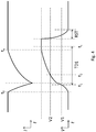
- Fig. 4 schematically shows a temporal change of the electric current flowing through the electrode (upper curve) caused by charge carriers generated by a radiation particle incident on the resistor, and a corresponding temporal change of the voltage of the electrode (lower curve).
- the voltage may be an integral of the electric current with respect to time.
- the radiation particle hits the resistor, charge carriers start being generated in the resistor, electric current starts to flow through the electrode of the resistor, and the absolute value of the voltage of the electrode or electrical contact starts to increase.
- the first voltage comparator 301 determines that the absolute value of the voltage equals or exceeds the absolute value of the first threshold V1, and the controller 310 starts the time delay TD1 and the controller 310 may deactivate the first voltage comparator 301 at the beginning of TD1. If the controller 310 is deactivated before t 1 , the controller 310 is activated at t 1 . During TD1, the controller 310 activates the second voltage comparator 302. The term "during" a time delay as used here means the beginning and the expiration (i.e., the end) and any time in between. For example, the controller 310 may activate the second voltage comparator 302 at the expiration of TD1.
- the controller 310 causes the number registered by the counter 320 to increase by one.
- time t e all charge carriers generated by the radiation particle drift out of the radiation absorption layer 110.
- time t s the time delay TD1 expires.
- time t s is after time t e ; namely TD1 expires after all charge carriers generated by the radiation particle drift out of the radiation absorption layer 110.
- the rate of change of the voltage is thus substantially zero at t s .
- the controller 310 may be configured to deactivate the second voltage comparator 302 at expiration of TD1 or at t 2 , or any time in between.
- the controller 310 may be configured to cause the voltmeter 306 to measure the voltage upon expiration of the time delay TD1. In an embodiment, the controller 310 causes the voltmeter 306 to measure the voltage after the rate of change of the voltage becomes substantially zero after the expiration of the time delay TD1. The voltage at this moment is proportional to the amount of charge carriers generated by a radiation particle, which relates to the energy of the X-ray photon. The controller 310 may be configured to determine the energy of the radiation particle based on voltage the voltmeter 306 measures. One way to determine the energy is by binning the voltage. The counter 320 may have a sub-counter for each bin.
- the controller 310 may cause the number registered in the sub-counter for that bin to increase by one. Therefore, the system 121 may be able to detect a radiation image and may be able to resolve energies of each radiation particle.
- the controller 310 After TD1 expires, the controller 310 connects the electrode to an electric ground for a reset period RST to allow charge carriers accumulated on the electrode to flow to the ground and reset the voltage. After RST, the system 121 is ready to detect another incident radiation particle. Implicitly, the rate of incident radiation particles the system 121 can handle in the example of Fig. 4 is limited by 1/(TD1+RST). If the first voltage comparator 301 has been deactivated, the controller 310 can activate it at any time before RST expires. If the controller 310 has been deactivated, it may be activated before RST expires.
- Fig. 5 schematically shows a temporal change of the electric current flowing through the electrode (upper curve) caused by noise (e.g., dark current, background radiation, scattered radiation, fluorescent X-rays, shared charges from adjacent pixels), and a corresponding temporal change of the voltage of the electrode (lower curve), in the system 121 operating in the way shown in Fig. 4 .
- noise e.g., dark current, background radiation, scattered radiation, fluorescent X-rays, shared charges from adjacent pixels
- the noise e.g., dark current, background radiation, scattered radiation, fluorescent X-rays, shared charges from adjacent pixels
- the controller 310 If the noise is large enough to cause the absolute value of the voltage to exceed the absolute value of V1 at time t 1 as determined by the first voltage comparator 301, the controller 310 starts the time delay TD1 and the controller 310 may deactivate the first voltage comparator 301 at the beginning of TD1. During TD1 (e.g., at expiration of TD1), the controller 310 activates the second voltage comparator 302. The noise is very unlikely large enough to cause the absolute value of the voltage to exceed the absolute value of V2 during TD1. Therefore, the controller 310 does not cause the number registered by the counter 320 to increase. At time t e , the noise ends. At time t s , the time delay TD1 expires.
- the controller 310 may be configured to deactivate the second voltage comparator 302 at expiration of TD1.
- the controller 310 may be configured not to cause the voltmeter 306 to measure the voltage if the absolute value of the voltage does not exceed the absolute value of V2 during TD1.
- the controller 310 connects the electrode to an electric ground for a reset period RST to allow charge carriers accumulated on the electrode as a result of the noise to flow to the ground and reset the voltage. Therefore, the system 121 may be very effective in noise rejection.
- Fig. 6 schematically shows a temporal change of the electric current flowing through the electrode (upper curve) caused by charge carriers generated by a radiation particle incident on the resistor, and a corresponding temporal change of the voltage of the electrode (lower curve), when the system 121 operates to detect incident radiation particles at a rate higher than 1/(TD1+RST).
- the voltage may be an integral of the electric current with respect to time.
- the radiation particle hits the resistor, charge carriers start being generated in the resistor, electric current starts to flow through the electrical contact of resistor, and the absolute value of the voltage of the electrode or the electrical contact starts to increase.
- the first voltage comparator 301 determines that the absolute value of the voltage equals or exceeds the absolute value of the first threshold V1, and the controller 310 starts a time delay TD2 shorter than TD1, and the controller 310 may deactivate the first voltage comparator 301 at the beginning of TD2. If the controller 310 is deactivated before t 1 , the controller 310 is activated at t 1 . During TD2 (e.g., at expiration of TD2), the controller 310 activates the second voltage comparator 302.
- the controller 310 causes the number registered by the counter 320 to increase by one.
- time t e all charge carriers generated by the radiation particle drift out of the radiation absorption layer 110.
- time t h the time delay TD2 expires.
- time t h is before time t e ; namely TD2 expires before all charge carriers generated by the radiation particle drift out of the radiation absorption layer 110.
- the rate of change of the voltage is thus substantially non-zero at t h .
- the controller 310 may be configured to deactivate the second voltage comparator 302 at expiration of TD2 or at t 2 , or any time in between.
- the controller 310 may be configured to extrapolate the voltage at t e from the voltage as a function of time during TD2 and use the extrapolated voltage to determine the energy of the radiation particle.
- the controller 310 connects the electrode to an electric ground for a reset period RST to allow charge carriers accumulated on the electrode to flow to the ground and reset the voltage.
- RST expires before t e .
- the rate of change of the voltage after RST may be substantially non-zero because all charge carriers generated by the radiation particle have not drifted out of the radiation absorption layer 110 upon expiration of RST before t e .
- the rate of change of the voltage becomes substantially zero after t e and the voltage stabilized to a residue voltage VR after t e .
- RST expires at or after t e , and the rate of change of the voltage after RST may be substantially zero because all charge carriers generated by the radiation particle drift out of the radiation absorption layer 110 at t e .
- the system 121 is ready to detect another incident radiation particle. If the first voltage comparator 301 has been deactivated, the controller 310 can activate it at any time before RST expires. If the controller 310 has been deactivated, it may be activated before RST expires.
- Fig. 7 schematically shows a temporal change of the electric current flowing through the electrode (upper curve) caused by noise (e.g., dark current, background radiation, scattered radiation, fluorescent X-rays, shared charges from adjacent pixels), and a corresponding temporal change of the voltage of the electrode (lower curve), in the system 121 operating in the way shown in Fig. 6 .
- noise e.g., dark current, background radiation, scattered radiation, fluorescent X-rays, shared charges from adjacent pixels
- the noise e.g., dark current, background radiation, scattered radiation, fluorescent X-rays, shared charges from adjacent pixels
- the controller 310 If the noise is large enough to cause the absolute value of the voltage to exceed the absolute value of V1 at time t 1 as determined by the first voltage comparator 301, the controller 310 starts the time delay TD2 and the controller 310 may deactivate the first voltage comparator 301 at the beginning of TD2. During TD2 (e.g., at expiration of TD2), the controller 310 activates the second voltage comparator 302. The noise is very unlikely large enough to cause the absolute value of the voltage to exceed the absolute value of V2 during TD2. Therefore, the controller 310 does not cause the number registered by the counter 320 to increase. At time t e , the noise ends. At time t h , the time delay TD2 expires.
- the controller 310 may be configured to deactivate the second voltage comparator 302 at expiration of TD2. After TD2 expires, the controller 310 connects the electrode to an electric ground for a reset period RST to allow charge carriers accumulated on the electrode as a result of the noise to flow to the ground and reset the voltage. Therefore, the system 121 may be very effective in noise rejection.
- Fig. 8 schematically shows a temporal change of the electric current flowing through the electrode (upper curve) caused by charge carriers generated by a series of radiation particles incident on the resistor, and a corresponding temporal change of the voltage of the electrode (lower curve), in the system 121 operating in the way shown in Fig. 6 with RST expires before t e .
- the voltage curve caused by charge carriers generated by each incident radiation particle is offset by the residue voltage before that radiation particle.
- the absolute value of the residue voltage successively increases with each incident photon. When the absolute value of the residue voltage exceeds V1 (see the dotted rectangle in Fig. 8 ), the controller starts the time delay TD2 and the controller 310 may deactivate the first voltage comparator 301 at the beginning of TD2.
- the controller connects the electrode to the electrical ground during the reset time period RST at the end of TD2, thereby resetting the residue voltage.
- the residue voltage thus does not cause an increase of the number registered by the counter 320.
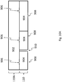
- Fig. 9A schematically shows a bottom view of a semiconductor wafer 902 with a plurality of semiconductor single crystal chunks 904 bonded thereon.
- the semiconductor single crystal chunks 904 may be cut from one or more manufactured semiconductor single crystals. They may be arranged on the semiconductor wafer 902 and fixed thereon. The arrangement need not have a high precision.
- the bonding may be by glue, plastic molding, or other known mechanism or techniques to be developed.
- there may be gaps between neighboring single crystal chunks 904 on the semiconductor wafer 902 and the widths of the gaps may not be the same.
- This bonding of semiconductor single crystals to a wafer may be referred to as wafer reconstruction.
- the semiconductor single crystal chunks may be CdZnTe chunks that are suitable to make radiation detectors.
- the CdZnTe chunks may have size of less than 1 cm, around 1 cm or larger than 1 cm.
- the semiconductor single crystal chunks 904 as shown in Fig. 9A are rectangular or square, but in some embodiments, some of the chunks 904 may have various other shapes, such as but not limited to, round, parallelogram, or irregular shapes.
- the semiconductor wafer 902 may be conductive.
- the size of the wafer 902 may be any suitable size, for example, 4 inches, 5 inches, 6 inches, 8 inches, 12 inches, or 18 inches.
- Fig. 9B schematically shows a cross-sectional view of the semiconductor wafer 902 and the plurality of semiconductor single crystal chunks 904 according to one embodiment.
- each semiconductor single crystal chunks 904 may have a first surface 906 bonded to the semiconductor wafer 902 and a second surface 908 opposite to the first surface 906.
- a gap 910 is shown in Fig. 9B to illustrate that there may be gaps between neighboring chunks 904.
- the semiconductor wafer 902 may be conductive and form a common electrode for the plurality of semiconductor single crystal chunks 904, while the plurality of semiconductor single crystal chunks 904 may for a radiation absorption layer 110. That is, the semiconductor wafer 902 may be an embodiment of the electrical contact 119A shown in Fig. 1B .
- the semiconductor single crystal chunks 904 may have a thickness of around 1 to 2 mm before being polished. As shown in Fig. 9B , the semiconductor single crystal chunks 904 may have different thicknesses.
- Fig. 10A schematically shows a semiconductor wafer 902 with a plurality of semiconductor single crystal chunks 904 bonded thereon, according to an embodiment.
- the plurality of semiconductor single crystal chunks 904 may have the same thickness.
- the same thickness of the plurality of semiconductor single crystal chunks 904 may be obtained by polishing after they have been bonded on the semiconductor wafer 902.
- Fig. 10B schematically shows electrodes 912 on the plurality of semiconductor single crystal chunks 904 of Fig. 10A , according to an embodiment.
- Each of the chunks 904 may have a plurality of electrodes 912.
- the electrodes 912 may be obtained using semiconductor wafer processes.
- the electrodes 912 may be generated using known or yet to be developed semiconductor wafer processes.
- Each chunk 904 may have a plurality of electrodes, for example, hundreds or thousands of electrodes. In one embodiment, each chunk 904 may have about 5000 electrodes.
- Fig. 10C schematically shows pillars 914 deposited on the plurality of semiconductor single crystal chunks 904.
- the pillars 914 may be conductive, for example, made of copper.
- the pillars 914 may be deposited using semiconductor wafer processes.
- the pillars 914 may be obtained using known or to be developed semiconductor wafer processes.
- Fig. 10D schematically shows that the plurality of semiconductor single crystal chunks 904 may be bonded to a second semiconductor wafer 920 by the pillars 914, according to an embodiment.
- the semiconductor wafer 920 may comprise the electronics layer 120 as described herein.
- the semiconductor wafer 920 may comprise a plurality of ASIC to read out and process the signals from the plurality of semiconductor single crystal chunks.
- the bonding may be a wafer level bonding and performed using room temperature bonding.
- the final product of the processes 9A-9B and 10A-10D may be used as one radiation detector 100 or may be cut into smaller modules such that each smaller module may be used as a radiation detector 100.
- Fig. 11 shows a flow chart of a process 1100 of making a semiconductor radiation detector (e.g., detector 100) as described herein.
- the process 1100 may start at block 1102, in which a plurality of semiconductor single crystal chunks (e.g., chunks 904) may be obtained.
- a plurality of semiconductor single crystal chunks e.g., chunks 904
- Each of the plurality of semiconductor single crystal chunk may have a first surface and a second surface, and the second surface may be on an opposite side to the first surface.
- the plurality of semiconductor single crystal chunks may be bonded to a first semiconductor wafer (e.g., wafer 902) by respective first surfaces.
- a plurality of electrodes may be formed on respective second surfaces of each of the plurality of semiconductor single crystal chunks.
- pillars e.g., pillars 914
- the semiconductor single crystal chunks may be CdZnTe chunks.
- Figs. 12-18 schematically show various systems each comprising an image sensor 9000.
- the image sensor 9000 may be an embodiment of an image sensor comprising one or more semiconductor radiation detectors described herein.
- a radiation detector according to an embodiment may be used to detect one or more types of radiation and X-ray is just one example.
- the radiation may be an electromagnetic radiation such as infrared light, visible light, ultraviolet light, X-ray or ⁇ -ray.
- the radiation may be of other types such as charged and non-charged particles as described herein.
- Fig. 12 schematically shows a system comprising the image sensor 9000 described herein.
- the system may be used for medical imaging such as chest X-ray radiography, abdominal X-ray radiography, etc.
- the system comprises an X-ray source 1201.
- X-ray emitted from the X-ray source 1201 penetrates an object 1202 (e.g., a human body part such as chest, limb, abdomen), is attenuated by different degrees by the internal structures of the object 1202 (e.g., bones, muscle, fat and organs, etc.), and is projected to the image sensor 9000.
- the image sensor 9000 forms an image by detecting the intensity distribution of the X-ray.
- Fig. 13 schematically shows a system comprising the image sensor 9000 described herein.
- the system may be used for medical imaging such as dental X-ray radiography.
- the system comprises an X-ray source 1301.
- X-ray emitted from the X-ray source 1301 penetrates an object 1302 that is part of a mammal (e.g., human) mouth.
- the object 1302 may include a maxilla bone, a palate bone, a tooth, the mandible, or the tongue.
- the X-ray is attenuated by different degrees by the different structures of the object 1302 and is projected to the image sensor 9000.
- the image sensor 9000 forms an image by detecting the intensity distribution of the X-ray. Teeth absorb X-ray more than dental caries, infections, periodontal ligament.
- the dosage of X-ray radiation received by a dental patient is typically small (around 0.150 mSv for a full mouth series).
- Fig. 14 schematically shows a cargo scanning or non-intrusive inspection (NII) system comprising the image sensor 9000 described herein.
- the system may be used for inspecting and identifying goods in transportation systems such as shipping containers, vehicles, ships, luggage, etc.
- the system comprises an X-ray source 1401.
- X-ray emitted from the X-ray source 1401 may backscatter from an object 1402 (e.g., shipping containers, vehicles, ships, etc.) and be projected to the image sensor 9000.
- object 1402 e.g., shipping containers, vehicles, ships, etc.
- Different internal structures of the object 1402 may backscatter X-ray differently.
- the image sensor 9000 forms an image by detecting the intensity distribution of the backscattered X-ray and/or energies of the backscattered X-ray photons.
- Fig. 15 schematically shows another cargo scanning or non-intrusive inspection (NII) system comprising the image sensor 9000 described herein.
- the system may be used for luggage screening at public transportation stations and airports.
- the system comprises an X-ray source 1501. X-ray emitted from the X-ray source 1501 may penetrate a piece of luggage 1502, be differently attenuated by the contents of the luggage, and projected to the image sensor 9000.
- the image sensor 9000 forms an image by detecting the intensity distribution of the transmitted X-ray.
- the system may reveal contents of luggage and identify items forbidden on public transportation, such as firearms, narcotics, edged weapons, flammables.
- Fig. 16 schematically shows a full-body scanner system comprising the image sensor 9000 described herein.
- the full-body scanner system may detect objects on a person's body for security screening purposes, without physically removing clothes or making physical contact.
- the full-body scanner system may be able to detect non-metal objects.
- the full-body scanner system comprises an X-ray source 1601. X-ray emitted from the X-ray source 1601 may backscatter from a human 1602 being screened and objects thereon, and be projected to the image sensor 9000. The objects and the human body may backscatter X-ray differently.
- the image sensor 9000 forms an image by detecting the intensity distribution of the backscattered X-ray.
- the image sensor 9000 and the X-ray source 1601 may be configured to scan the human in a linear or rotational direction.
- Fig. 17 schematically shows an X-ray computed tomography (X-ray CT) system.
- the X-ray CT system uses computer-processed X-rays to produce tomographic images (virtual "slices") of specific areas of a scanned object.
- the tomographic images may be used for diagnostic and therapeutic purposes in various medical disciplines, or for flaw detection, failure analysis, metrology, assembly analysis and reverse engineering.
- the X-ray CT system comprises the image sensor 9000 described herein and an X-ray source 1701.
- the image sensor 9000 and the X-ray source 1701 may be configured to rotate synchronously along one or more circular or spiral paths.
- Fig. 18 schematically shows an electron microscope.
- the electron microscope comprises an electron source 1801 (also called an electron gun) that is configured to emit electrons.
- the electron source 1801 may have various emission mechanisms such as thermionic, photocathode, cold emission, or plasmas source.
- the emitted electrons pass through an electronic optical system 1803, which may be configured to shape, accelerate, or focus the electrons.
- the electrons then reach a sample 1802 and an image detector may form an image therefrom.
- the electron microscope may comprise the image sensor 9000 described herein, for performing energy-dispersive X-ray spectroscopy (EDS).
- EDS is an analytical technique used for the elemental analysis or chemical characterization of a sample.
- the electrons incident on a sample they cause emission of characteristic X-rays from the sample.
- the incident electrons may excite an electron in an inner shell of an atom in the sample, ejecting it from the shell while creating an electron hole where the electron was.
- An electron from an outer, higher-energy shell then fills the hole, and the difference in energy between the higher-energy shell and the lower energy shell may be released in the form of an X-ray.
- the number and energy of the X-rays emitted from the sample can be measured by the image sensor 9000.
- the image sensor 9000 described here may have other applications such as in an X-ray telescope, X-ray mammography, industrial X-ray defect detection, X-ray microscopy or microradiography, X-ray casting inspection, X-ray non-destructive testing, X-ray weld inspection, X-ray digital subtraction angiography, etc. It may be suitable to use this image sensor 9000 in place of a photographic plate, a photographic film, a PSP plate, an X-ray image intensifier, a scintillator, or another semiconductor X-ray detector.
Landscapes
- Engineering & Computer Science (AREA)
- Physics & Mathematics (AREA)
- Power Engineering (AREA)
- General Physics & Mathematics (AREA)
- Electromagnetism (AREA)
- Condensed Matter Physics & Semiconductors (AREA)
- Computer Hardware Design (AREA)
- Microelectronics & Electronic Packaging (AREA)
- Health & Medical Sciences (AREA)
- Life Sciences & Earth Sciences (AREA)
- Medical Informatics (AREA)
- High Energy & Nuclear Physics (AREA)
- Molecular Biology (AREA)
- Chemical & Material Sciences (AREA)
- Manufacturing & Machinery (AREA)
- Biomedical Technology (AREA)
- Animal Behavior & Ethology (AREA)
- Biophysics (AREA)
- Toxicology (AREA)
- Nuclear Medicine, Radiotherapy & Molecular Imaging (AREA)
- Optics & Photonics (AREA)
- Pathology (AREA)
- Radiology & Medical Imaging (AREA)
- Spectroscopy & Molecular Physics (AREA)
- Heart & Thoracic Surgery (AREA)
- Surgery (AREA)
- Veterinary Medicine (AREA)
- General Health & Medical Sciences (AREA)
- Public Health (AREA)
- Theoretical Computer Science (AREA)
- Pulmonology (AREA)
- Inorganic Chemistry (AREA)
- Analytical Chemistry (AREA)
- Dentistry (AREA)
- Oral & Maxillofacial Surgery (AREA)
- Measurement Of Radiation (AREA)
- Solid State Image Pick-Up Elements (AREA)
- Light Receiving Elements (AREA)
Claims (15)
- Procédé de fabrication d'un appareil adapté à la détection de rayons X, le procédé comprenant :l'obtention d'une pluralité de fragments monocristallins semi-conducteurs (904) ayant chacun une première surface (906) et une seconde surface (908), la seconde surface étant opposée à la première surface ;la liaison de la pluralité de fragments monocristallins semi-conducteurs par des premières surfaces respectives à une première tranche de semi-conducteur (902), la pluralité de fragments monocristallins semi-conducteurs formant une couche d'absorption de rayonnement (110), formant une pluralité d'électrodes (912) sur des secondes surfaces respectives de chacun de la pluralité de fragments monocristallins semi-conducteurs ;le dépôt des piliers (914) sur chacun de la pluralité de fragments monocristallins semi-conducteurs ; etla liaison de la pluralité de blocs monocristallins semi-conducteurs à une seconde tranche de semi-conducteur (920) par les piliers, caractérisé en ce que la pluralité de fragments monocristallins semi-conducteurs ont des tailles et des espaces différents entre eux.
- Procédé selon la revendication 1, dans lequel la pluralité de fragments monocristallins semi-conducteurs sont des fragments de tellurure de cadmium-zinc (CdZnTe).
- Procédé selon la revendication 1, comprenant en outre le polissage des secondes surfaces de la pluralité de fragments monocristallins semi-conducteurs de sorte que la pluralité de fragments monocristallins semi-conducteurs soient de la même épaisseur.
- Procédé selon la revendication 1, dans lequel la première tranche de semi-conducteur forme une électrode commune pour la pluralité de fragments monocristallins semi-conducteurs.
- Procédé selon la revendication 1, dans lequel la couche d'absorption de rayonnement est configurée pour absorber un rayonnement électromagnétique ou un rayonnement de particules.
- Procédé selon la revendication 1, dans lequel la seconde tranche de semi-conducteur comprend une couche électronique permettant de traiter des signaux générés dans la couche d'absorption de rayonnement, la couche électronique comprenant un système électronique connecté à l'une de la pluralité d'électrodes de la pluralité de fragments monocristallins semi-conducteurs, le système électronique comprend :un premier comparateur de tension configuré pour comparer une tension d'au moins une des électrodes à un premier seuil ;un second comparateur de tension configuré pour comparer la tension à un second seuil ;un compteur configuré pour enregistrer un certain nombre de photons de rayonnement ou de particules atteignant la couche d'absorption de rayonnement ;un dispositif de commande ;le dispositif de commande étant configuré pour démarrer une temporisation à partir d'un moment auquel le premier comparateur de tension détermine qu'une valeur absolue de la tension est égale ou supérieure à une valeur absolue du premier seuil ;le dispositif de commande étant configuré pour activer le second comparateur de tension pendant la temporisation ;le dispositif de commande étant configuré pour amener le nombre enregistré par le compteur à augmenter d'un, si le second comparateur de tension détermine qu'une valeur absolue de la tension est égale ou supérieure à une valeur absolue du second seuil.
- Procédé selon la revendication 6, dans lequel le système électronique comprend en outre un module de condensateur connecté électriquement à l'électrode, dans lequel le module de condensateur est configuré pour collecter des supports de charge à partir de l'électrode.
- Procédé selon la revendication 6, le dispositif de commande étant configuré pour activer le second comparateur de tensions au début ou à l'expiration de la temporisation.
- Procédé selon la revendication 6, dans lequel le système électronique comprend en outre un voltmètre, dans lequel le dispositif de commande est configuré pour amener le voltmètre à mesurer la tension à l'expiration de la temporisation.
- Procédé selon la revendication 6, dans lequel le dispositif de commande est configuré pour déterminer une énergie de particules de rayonnement sur la base d'une valeur de la tension mesurée à l'expiration de la temporisation.
- Procédé selon la revendication 6, dans lequel le dispositif de commande est configuré pour connecter l'électrode à une mise électrique à la terre.
- Procédé selon la revendication 6, dans lequel une vitesse de changement de la tension est sensiblement nulle à l'expiration de la temporisation.
- Dispositif (100) de détection d'un rayonnement, comprenant :une première tranche de semi-conducteur (902), une seconde tranche de semi-conducteur (920) et une pluralité de fragments monocristallins semi-conducteurs (904), la pluralité de fragments monocristallins semi-conducteurs formant une couche d'absorption de rayonnement (110) ;dans lequel chacun de la pluralité de fragments monocristallins semi-conducteurs a une première surface (906) et une seconde surface (908), la seconde surface étant opposée à la première surface, et la pluralité de fragments cristallins semi-conducteurs étant liés par des premières surfaces respectives à la première tranche de semi-conducteur,dans lequel une pluralité d'électrodes (912) sont formées sur des secondes surfaces respectives de chacun de la pluralité de fragments monocristallins semi-conducteurs ;et dans lequel la pluralité de fragments monocristallins semi-conducteurs sont liés à la seconde tranche de semi-conducteur par des piliers (912), caractérisé en ce que la pluralité de fragments cristallins semi-conducteurs ont des tailles et des espaces différents entre eux.
- Dispositif selon la revendication 13, dans lequel la pluralité de fragments monocristallins semi-conducteurs sont des fragments de tellurure de cadmium-zinc (CdZnTe).
- Système comprenant l'appareil selon l'une quelconque des revendications 13 à 14 et une source de rayonnement, dans lequel le système est configuré pour effectuer une radiographie sur la poitrine, l'abdomen ou la bouche humaine.
Applications Claiming Priority (1)
| Application Number | Priority Date | Filing Date | Title |
|---|---|---|---|
| PCT/CN2017/081400 WO2018191943A1 (fr) | 2017-04-21 | 2017-04-21 | Procédés de fabrication de détecteur de rayonnement à semi-conducteur |
Publications (3)
| Publication Number | Publication Date |
|---|---|
| EP3613085A1 EP3613085A1 (fr) | 2020-02-26 |
| EP3613085A4 EP3613085A4 (fr) | 2020-12-16 |
| EP3613085B1 true EP3613085B1 (fr) | 2021-11-24 |
Family
ID=63856452
Family Applications (1)
| Application Number | Title | Priority Date | Filing Date |
|---|---|---|---|
| EP17906435.7A Active EP3613085B1 (fr) | 2017-04-21 | 2017-04-21 | Détecteur de rayonnement à semi-conducteur et méthode de fabrication |
Country Status (5)
| Country | Link |
|---|---|
| US (2) | US10833217B2 (fr) |
| EP (1) | EP3613085B1 (fr) |
| CN (1) | CN110494989B (fr) |
| TW (1) | TWI813565B (fr) |
| WO (1) | WO2018191943A1 (fr) |
Families Citing this family (5)
| Publication number | Priority date | Publication date | Assignee | Title |
|---|---|---|---|---|
| CN108449982B (zh) * | 2015-08-27 | 2020-12-15 | 深圳帧观德芯科技有限公司 | 利用能够分辨光子能量的检测器的x射线成像 |
| EP3482231B1 (fr) * | 2016-07-05 | 2022-09-07 | Shenzhen Xpectvision Technology Co., Ltd. | Collage de matériaux à coefficients de dilatation thermique différents |
| EP3743738A4 (fr) * | 2018-01-24 | 2021-07-28 | Shenzhen Xpectvision Technology Co., Ltd. | Détecteur de pixels en bande |
| EP3909234A4 (fr) * | 2019-01-10 | 2022-06-15 | Shenzhen Xpectvision Technology Co., Ltd. | Capteur d'image comportant des détecteurs de rayonnement de différentes orientations |
| US11610757B2 (en) * | 2019-08-28 | 2023-03-21 | Kla Corporation | Sensor module for scanning electron microscopy applications |
Citations (1)
| Publication number | Priority date | Publication date | Assignee | Title |
|---|---|---|---|---|
| US20150276945A1 (en) * | 2014-03-25 | 2015-10-01 | Oy Ajat Ltd. | Semiconductor bump-bonded x-ray imaging device |
Family Cites Families (14)
| Publication number | Priority date | Publication date | Assignee | Title |
|---|---|---|---|---|
| US5368882A (en) * | 1993-08-25 | 1994-11-29 | Minnesota Mining And Manufacturing Company | Process for forming a radiation detector |
| EP1443569A2 (fr) * | 2003-01-30 | 2004-08-04 | Postech Foundation | Dispositif supraconducteur à radiation des ondes électromagnétiques |
| US8178422B2 (en) * | 2009-03-31 | 2012-05-15 | Taiwan Semiconductor Manufacturing Company, Ltd. | Method of measurement in semiconductor fabrication |
| JP2011086828A (ja) * | 2009-10-16 | 2011-04-28 | Sumco Corp | 半導体装置およびその製造方法 |
| CN103119929B (zh) * | 2010-09-13 | 2016-08-03 | 雷湾地区研究所 | 重置光导x射线成像检测器的系统和方法 |
| US20130026380A1 (en) * | 2011-07-26 | 2013-01-31 | General Electric Company | Radiation detector with angled surfaces and method of fabrication |
| US9337229B2 (en) * | 2013-12-26 | 2016-05-10 | Taiwan Semiconductor Manufacturing Company Ltd. | Semiconductor device and manufacturing method thereof |
| US20150243825A1 (en) * | 2014-02-27 | 2015-08-27 | Raytheon Company | Simultaneous dual-band detector |
| CN107735869A (zh) * | 2015-02-17 | 2018-02-23 | 瑞德兰科技有限公司 | 高性能辐射检测器和其制造方法 |
| WO2016161544A1 (fr) * | 2015-04-07 | 2016-10-13 | Shenzhen Xpectvision Technology Co.,Ltd. | Détecteur de rayons x à semi-conducteurs |
| JP6356351B2 (ja) * | 2015-05-26 | 2018-07-11 | シーメンス ヘルスケア ゲゼルシヤフト ミツト ベシユレンクテル ハフツング | 放射線検出装置 |
| WO2017041221A1 (fr) * | 2015-09-08 | 2017-03-16 | Shenzhen Xpectvision Technology Co., Ltd. | Procédés de fabrication d'un détecteur de rayons x |
| US10139500B2 (en) * | 2015-10-14 | 2018-11-27 | Shenzhen Xpectvision Technology Co., Ltd. | Semiconductor X-ray detector capable of dark current correction |
| WO2018133093A1 (fr) * | 2017-01-23 | 2018-07-26 | Shenzhen Xpectvision Technology Co., Ltd. | Procédés de fabrication de détecteur de rayons x à semi-conducteurs |
-
2017
- 2017-04-21 CN CN201780089443.4A patent/CN110494989B/zh active Active
- 2017-04-21 WO PCT/CN2017/081400 patent/WO2018191943A1/fr active Application Filing
- 2017-04-21 EP EP17906435.7A patent/EP3613085B1/fr active Active
-
2018
- 2018-04-17 TW TW107112963A patent/TWI813565B/zh active
-
2019
- 2019-09-09 US US16/565,458 patent/US10833217B2/en active Active
-
2020
- 2020-09-30 US US17/039,059 patent/US11380812B2/en active Active
Patent Citations (1)
| Publication number | Priority date | Publication date | Assignee | Title |
|---|---|---|---|---|
| US20150276945A1 (en) * | 2014-03-25 | 2015-10-01 | Oy Ajat Ltd. | Semiconductor bump-bonded x-ray imaging device |
Also Published As
| Publication number | Publication date |
|---|---|
| US20210013362A1 (en) | 2021-01-14 |
| EP3613085A4 (fr) | 2020-12-16 |
| US11380812B2 (en) | 2022-07-05 |
| TW201839424A (zh) | 2018-11-01 |
| US20200013919A1 (en) | 2020-01-09 |
| CN110494989A (zh) | 2019-11-22 |
| WO2018191943A1 (fr) | 2018-10-25 |
| EP3613085A1 (fr) | 2020-02-26 |
| CN110494989B (zh) | 2022-08-26 |
| TWI813565B (zh) | 2023-09-01 |
| US10833217B2 (en) | 2020-11-10 |
Similar Documents
| Publication | Publication Date | Title |
|---|---|---|
| US11013479B2 (en) | Semiconductor X-ray detector | |
| US11380812B2 (en) | Methods of making semiconductor radiation detector | |
| US10945688B2 (en) | X-ray imaging system and a method of X-ray imaging | |
| US20210185203A1 (en) | Image sensor having radiation detectors of different orientations | |
| US20210325319A1 (en) | Imaging system having radiation detectors of different orientations | |
| US11520064B2 (en) | X-ray detectors capable of identifying and managing charge sharing | |
| US20210321962A1 (en) | Image sensor having radiation detectors of different orientations | |
| EP3658961B1 (fr) | Détecteur de rayonnement et procédés de production de données par celui-ci | |
| US11032500B2 (en) | Dark noise compensation in a radiation detector | |
| WO2018053774A1 (fr) | Mise sous boîtier de détecteurs de rayons x à semiconducteurs | |
| US20210173104A1 (en) | Radiation detector with subpixels operating in different modes | |
| US11947059B2 (en) | Semiconductor x-ray detector |
Legal Events
| Date | Code | Title | Description |
|---|---|---|---|
| STAA | Information on the status of an ep patent application or granted ep patent |
Free format text: STATUS: THE INTERNATIONAL PUBLICATION HAS BEEN MADE |
|
| PUAI | Public reference made under article 153(3) epc to a published international application that has entered the european phase |
Free format text: ORIGINAL CODE: 0009012 |
|
| STAA | Information on the status of an ep patent application or granted ep patent |
Free format text: STATUS: REQUEST FOR EXAMINATION WAS MADE |
|
| 17P | Request for examination filed |
Effective date: 20191023 |
|
| AK | Designated contracting states |
Kind code of ref document: A1 Designated state(s): AL AT BE BG CH CY CZ DE DK EE ES FI FR GB GR HR HU IE IS IT LI LT LU LV MC MK MT NL NO PL PT RO RS SE SI SK SM TR |
|
| AX | Request for extension of the european patent |
Extension state: BA ME |
|
| RAP1 | Party data changed (applicant data changed or rights of an application transferred) |
Owner name: SHENZHEN XPECTVISION TECHNOLOGY CO., LTD. |
|
| DAV | Request for validation of the european patent (deleted) | ||
| DAX | Request for extension of the european patent (deleted) | ||
| A4 | Supplementary search report drawn up and despatched |
Effective date: 20201117 |
|
| RIC1 | Information provided on ipc code assigned before grant |
Ipc: G01T 1/24 20060101ALI20201111BHEP Ipc: H01L 31/08 20060101AFI20201111BHEP |
|
| REG | Reference to a national code |
Ref country code: DE Ref legal event code: R079 Ref document number: 602017050014 Country of ref document: DE Free format text: PREVIOUS MAIN CLASS: H01L0031080000 Ipc: H01L0031180000 |
|
| GRAP | Despatch of communication of intention to grant a patent |
Free format text: ORIGINAL CODE: EPIDOSNIGR1 |
|
| STAA | Information on the status of an ep patent application or granted ep patent |
Free format text: STATUS: GRANT OF PATENT IS INTENDED |
|
| RIC1 | Information provided on ipc code assigned before grant |
Ipc: H01L 27/146 20060101ALI20210730BHEP Ipc: H01L 31/18 20060101AFI20210730BHEP |
|
| INTG | Intention to grant announced |
Effective date: 20210831 |
|
| GRAA | (expected) grant |
Free format text: ORIGINAL CODE: 0009210 |
|
| STAA | Information on the status of an ep patent application or granted ep patent |
Free format text: STATUS: THE PATENT HAS BEEN GRANTED |
|
| GRAS | Grant fee paid |
Free format text: ORIGINAL CODE: EPIDOSNIGR3 |
|
| AK | Designated contracting states |
Kind code of ref document: B1 Designated state(s): AL AT BE BG CH CY CZ DE DK EE ES FI FR GB GR HR HU IE IS IT LI LT LU LV MC MK MT NL NO PL PT RO RS SE SI SK SM TR |
|
| REG | Reference to a national code |
Ref country code: GB Ref legal event code: FG4D |
|
| RIN1 | Information on inventor provided before grant (corrected) |
Inventor name: LIU, YURUN Inventor name: CAO, PEIYAN |
|
| REG | Reference to a national code |
Ref country code: AT Ref legal event code: REF Ref document number: 1450533 Country of ref document: AT Kind code of ref document: T Effective date: 20211215 |
|
| REG | Reference to a national code |
Ref country code: DE Ref legal event code: R096 Ref document number: 602017050014 Country of ref document: DE |
|
| REG | Reference to a national code |
Ref country code: IE Ref legal event code: FG4D |
|
| REG | Reference to a national code |
Ref country code: LT Ref legal event code: MG9D |
|
| REG | Reference to a national code |
Ref country code: NL Ref legal event code: MP Effective date: 20211124 |
|
| RAP4 | Party data changed (patent owner data changed or rights of a patent transferred) |
Owner name: SHENZHEN XPECTVISION TECHNOLOGY CO., LTD. |
|
| REG | Reference to a national code |
Ref country code: AT Ref legal event code: MK05 Ref document number: 1450533 Country of ref document: AT Kind code of ref document: T Effective date: 20211124 |
|
| PG25 | Lapsed in a contracting state [announced via postgrant information from national office to epo] |
Ref country code: RS Free format text: LAPSE BECAUSE OF FAILURE TO SUBMIT A TRANSLATION OF THE DESCRIPTION OR TO PAY THE FEE WITHIN THE PRESCRIBED TIME-LIMIT Effective date: 20211124 Ref country code: LT Free format text: LAPSE BECAUSE OF FAILURE TO SUBMIT A TRANSLATION OF THE DESCRIPTION OR TO PAY THE FEE WITHIN THE PRESCRIBED TIME-LIMIT Effective date: 20211124 Ref country code: FI Free format text: LAPSE BECAUSE OF FAILURE TO SUBMIT A TRANSLATION OF THE DESCRIPTION OR TO PAY THE FEE WITHIN THE PRESCRIBED TIME-LIMIT Effective date: 20211124 Ref country code: BG Free format text: LAPSE BECAUSE OF FAILURE TO SUBMIT A TRANSLATION OF THE DESCRIPTION OR TO PAY THE FEE WITHIN THE PRESCRIBED TIME-LIMIT Effective date: 20220224 Ref country code: AT Free format text: LAPSE BECAUSE OF FAILURE TO SUBMIT A TRANSLATION OF THE DESCRIPTION OR TO PAY THE FEE WITHIN THE PRESCRIBED TIME-LIMIT Effective date: 20211124 |
|
| PG25 | Lapsed in a contracting state [announced via postgrant information from national office to epo] |
Ref country code: IS Free format text: LAPSE BECAUSE OF FAILURE TO SUBMIT A TRANSLATION OF THE DESCRIPTION OR TO PAY THE FEE WITHIN THE PRESCRIBED TIME-LIMIT Effective date: 20220324 Ref country code: SE Free format text: LAPSE BECAUSE OF FAILURE TO SUBMIT A TRANSLATION OF THE DESCRIPTION OR TO PAY THE FEE WITHIN THE PRESCRIBED TIME-LIMIT Effective date: 20211124 Ref country code: PT Free format text: LAPSE BECAUSE OF FAILURE TO SUBMIT A TRANSLATION OF THE DESCRIPTION OR TO PAY THE FEE WITHIN THE PRESCRIBED TIME-LIMIT Effective date: 20220324 Ref country code: PL Free format text: LAPSE BECAUSE OF FAILURE TO SUBMIT A TRANSLATION OF THE DESCRIPTION OR TO PAY THE FEE WITHIN THE PRESCRIBED TIME-LIMIT Effective date: 20211124 Ref country code: NO Free format text: LAPSE BECAUSE OF FAILURE TO SUBMIT A TRANSLATION OF THE DESCRIPTION OR TO PAY THE FEE WITHIN THE PRESCRIBED TIME-LIMIT Effective date: 20220224 Ref country code: NL Free format text: LAPSE BECAUSE OF FAILURE TO SUBMIT A TRANSLATION OF THE DESCRIPTION OR TO PAY THE FEE WITHIN THE PRESCRIBED TIME-LIMIT Effective date: 20211124 Ref country code: LV Free format text: LAPSE BECAUSE OF FAILURE TO SUBMIT A TRANSLATION OF THE DESCRIPTION OR TO PAY THE FEE WITHIN THE PRESCRIBED TIME-LIMIT Effective date: 20211124 Ref country code: HR Free format text: LAPSE BECAUSE OF FAILURE TO SUBMIT A TRANSLATION OF THE DESCRIPTION OR TO PAY THE FEE WITHIN THE PRESCRIBED TIME-LIMIT Effective date: 20211124 Ref country code: GR Free format text: LAPSE BECAUSE OF FAILURE TO SUBMIT A TRANSLATION OF THE DESCRIPTION OR TO PAY THE FEE WITHIN THE PRESCRIBED TIME-LIMIT Effective date: 20220225 Ref country code: ES Free format text: LAPSE BECAUSE OF FAILURE TO SUBMIT A TRANSLATION OF THE DESCRIPTION OR TO PAY THE FEE WITHIN THE PRESCRIBED TIME-LIMIT Effective date: 20211124 |
|
| PG25 | Lapsed in a contracting state [announced via postgrant information from national office to epo] |
Ref country code: SM Free format text: LAPSE BECAUSE OF FAILURE TO SUBMIT A TRANSLATION OF THE DESCRIPTION OR TO PAY THE FEE WITHIN THE PRESCRIBED TIME-LIMIT Effective date: 20211124 Ref country code: SK Free format text: LAPSE BECAUSE OF FAILURE TO SUBMIT A TRANSLATION OF THE DESCRIPTION OR TO PAY THE FEE WITHIN THE PRESCRIBED TIME-LIMIT Effective date: 20211124 Ref country code: RO Free format text: LAPSE BECAUSE OF FAILURE TO SUBMIT A TRANSLATION OF THE DESCRIPTION OR TO PAY THE FEE WITHIN THE PRESCRIBED TIME-LIMIT Effective date: 20211124 Ref country code: EE Free format text: LAPSE BECAUSE OF FAILURE TO SUBMIT A TRANSLATION OF THE DESCRIPTION OR TO PAY THE FEE WITHIN THE PRESCRIBED TIME-LIMIT Effective date: 20211124 Ref country code: DK Free format text: LAPSE BECAUSE OF FAILURE TO SUBMIT A TRANSLATION OF THE DESCRIPTION OR TO PAY THE FEE WITHIN THE PRESCRIBED TIME-LIMIT Effective date: 20211124 Ref country code: CZ Free format text: LAPSE BECAUSE OF FAILURE TO SUBMIT A TRANSLATION OF THE DESCRIPTION OR TO PAY THE FEE WITHIN THE PRESCRIBED TIME-LIMIT Effective date: 20211124 |
|
| REG | Reference to a national code |
Ref country code: DE Ref legal event code: R097 Ref document number: 602017050014 Country of ref document: DE |
|
| PLBE | No opposition filed within time limit |
Free format text: ORIGINAL CODE: 0009261 |
|
| STAA | Information on the status of an ep patent application or granted ep patent |
Free format text: STATUS: NO OPPOSITION FILED WITHIN TIME LIMIT |
|
| PG25 | Lapsed in a contracting state [announced via postgrant information from national office to epo] |
Ref country code: AL Free format text: LAPSE BECAUSE OF FAILURE TO SUBMIT A TRANSLATION OF THE DESCRIPTION OR TO PAY THE FEE WITHIN THE PRESCRIBED TIME-LIMIT Effective date: 20211124 |
|
| 26N | No opposition filed |
Effective date: 20220825 |
|
| PG25 | Lapsed in a contracting state [announced via postgrant information from national office to epo] |
Ref country code: SI Free format text: LAPSE BECAUSE OF FAILURE TO SUBMIT A TRANSLATION OF THE DESCRIPTION OR TO PAY THE FEE WITHIN THE PRESCRIBED TIME-LIMIT Effective date: 20211124 |
|
| REG | Reference to a national code |
Ref country code: CH Ref legal event code: PL |
|
| REG | Reference to a national code |
Ref country code: BE Ref legal event code: MM Effective date: 20220430 |
|
| PG25 | Lapsed in a contracting state [announced via postgrant information from national office to epo] |
Ref country code: MC Free format text: LAPSE BECAUSE OF FAILURE TO SUBMIT A TRANSLATION OF THE DESCRIPTION OR TO PAY THE FEE WITHIN THE PRESCRIBED TIME-LIMIT Effective date: 20211124 Ref country code: LU Free format text: LAPSE BECAUSE OF NON-PAYMENT OF DUE FEES Effective date: 20220421 Ref country code: LI Free format text: LAPSE BECAUSE OF NON-PAYMENT OF DUE FEES Effective date: 20220430 Ref country code: CH Free format text: LAPSE BECAUSE OF NON-PAYMENT OF DUE FEES Effective date: 20220430 |
|
| PG25 | Lapsed in a contracting state [announced via postgrant information from national office to epo] |
Ref country code: BE Free format text: LAPSE BECAUSE OF NON-PAYMENT OF DUE FEES Effective date: 20220430 |
|
| PG25 | Lapsed in a contracting state [announced via postgrant information from national office to epo] |
Ref country code: IE Free format text: LAPSE BECAUSE OF NON-PAYMENT OF DUE FEES Effective date: 20220421 |
|
| PG25 | Lapsed in a contracting state [announced via postgrant information from national office to epo] |
Ref country code: IT Free format text: LAPSE BECAUSE OF FAILURE TO SUBMIT A TRANSLATION OF THE DESCRIPTION OR TO PAY THE FEE WITHIN THE PRESCRIBED TIME-LIMIT Effective date: 20211124 |
|
| P01 | Opt-out of the competence of the unified patent court (upc) registered |
Effective date: 20230522 |
|
| PGFP | Annual fee paid to national office [announced via postgrant information from national office to epo] |
Ref country code: FR Payment date: 20230425 Year of fee payment: 7 Ref country code: DE Payment date: 20230412 Year of fee payment: 7 |
|
| PGFP | Annual fee paid to national office [announced via postgrant information from national office to epo] |
Ref country code: GB Payment date: 20230424 Year of fee payment: 7 |
|
| PG25 | Lapsed in a contracting state [announced via postgrant information from national office to epo] |
Ref country code: MK Free format text: LAPSE BECAUSE OF FAILURE TO SUBMIT A TRANSLATION OF THE DESCRIPTION OR TO PAY THE FEE WITHIN THE PRESCRIBED TIME-LIMIT Effective date: 20211124 Ref country code: CY Free format text: LAPSE BECAUSE OF FAILURE TO SUBMIT A TRANSLATION OF THE DESCRIPTION OR TO PAY THE FEE WITHIN THE PRESCRIBED TIME-LIMIT Effective date: 20211124 |