EP3613074B1 - Method for joining a microelectronic chip to a wire element - Google Patents
Method for joining a microelectronic chip to a wire element Download PDFInfo
- Publication number
- EP3613074B1 EP3613074B1 EP18719983.1A EP18719983A EP3613074B1 EP 3613074 B1 EP3613074 B1 EP 3613074B1 EP 18719983 A EP18719983 A EP 18719983A EP 3613074 B1 EP3613074 B1 EP 3613074B1
- Authority
- EP
- European Patent Office
- Prior art keywords
- face
- chip
- cover
- wire element
- joining method
- Prior art date
- Legal status (The legal status is an assumption and is not a legal conclusion. Google has not performed a legal analysis and makes no representation as to the accuracy of the status listed.)
- Active
Links
- 238000004377 microelectronic Methods 0.000 title claims description 68
- 238000000034 method Methods 0.000 title claims description 59
- 238000005304 joining Methods 0.000 title claims description 21
- 239000000463 material Substances 0.000 claims description 27
- 239000000853 adhesive Substances 0.000 claims description 16
- 230000001070 adhesive effect Effects 0.000 claims description 16
- 238000003780 insertion Methods 0.000 claims description 14
- 230000037431 insertion Effects 0.000 claims description 14
- 238000010438 heat treatment Methods 0.000 claims description 13
- 239000004020 conductor Substances 0.000 claims description 9
- 230000003014 reinforcing effect Effects 0.000 claims description 2
- 239000000126 substance Substances 0.000 description 13
- RYGMFSIKBFXOCR-UHFFFAOYSA-N Copper Chemical compound [Cu] RYGMFSIKBFXOCR-UHFFFAOYSA-N 0.000 description 6
- 239000010949 copper Substances 0.000 description 6
- 229910052802 copper Inorganic materials 0.000 description 6
- 238000004519 manufacturing process Methods 0.000 description 6
- 230000008018 melting Effects 0.000 description 6
- 238000002844 melting Methods 0.000 description 6
- 239000000758 substrate Substances 0.000 description 6
- 238000005538 encapsulation Methods 0.000 description 5
- 229910045601 alloy Inorganic materials 0.000 description 4
- 239000000956 alloy Substances 0.000 description 4
- 229910052751 metal Inorganic materials 0.000 description 4
- 239000002184 metal Substances 0.000 description 4
- 239000004753 textile Substances 0.000 description 4
- 238000011282 treatment Methods 0.000 description 4
- 230000008901 benefit Effects 0.000 description 3
- 230000002787 reinforcement Effects 0.000 description 3
- 238000005476 soldering Methods 0.000 description 3
- BQCADISMDOOEFD-UHFFFAOYSA-N Silver Chemical compound [Ag] BQCADISMDOOEFD-UHFFFAOYSA-N 0.000 description 2
- ATJFFYVFTNAWJD-UHFFFAOYSA-N Tin Chemical compound [Sn] ATJFFYVFTNAWJD-UHFFFAOYSA-N 0.000 description 2
- 239000011248 coating agent Substances 0.000 description 2
- 238000000576 coating method Methods 0.000 description 2
- 230000000295 complement effect Effects 0.000 description 2
- 238000005520 cutting process Methods 0.000 description 2
- 238000005516 engineering process Methods 0.000 description 2
- 238000005530 etching Methods 0.000 description 2
- 230000006698 induction Effects 0.000 description 2
- 230000010354 integration Effects 0.000 description 2
- 239000007788 liquid Substances 0.000 description 2
- 230000005226 mechanical processes and functions Effects 0.000 description 2
- 150000002739 metals Chemical class 0.000 description 2
- 229920000642 polymer Polymers 0.000 description 2
- 230000005855 radiation Effects 0.000 description 2
- 230000002040 relaxant effect Effects 0.000 description 2
- 229910052709 silver Inorganic materials 0.000 description 2
- 239000004332 silver Substances 0.000 description 2
- 239000010935 stainless steel Substances 0.000 description 2
- 229910001220 stainless steel Inorganic materials 0.000 description 2
- 239000011135 tin Substances 0.000 description 2
- 229910052718 tin Inorganic materials 0.000 description 2
- VYZAMTAEIAYCRO-UHFFFAOYSA-N Chromium Chemical compound [Cr] VYZAMTAEIAYCRO-UHFFFAOYSA-N 0.000 description 1
- VYPSYNLAJGMNEJ-UHFFFAOYSA-N Silicium dioxide Chemical compound O=[Si]=O VYPSYNLAJGMNEJ-UHFFFAOYSA-N 0.000 description 1
- 230000005540 biological transmission Effects 0.000 description 1
- 230000015572 biosynthetic process Effects 0.000 description 1
- 239000000919 ceramic Substances 0.000 description 1
- 239000011651 chromium Substances 0.000 description 1
- 229910052804 chromium Inorganic materials 0.000 description 1
- 150000001875 compounds Chemical class 0.000 description 1
- 230000008021 deposition Effects 0.000 description 1
- 239000000835 fiber Substances 0.000 description 1
- 239000012530 fluid Substances 0.000 description 1
- 230000004907 flux Effects 0.000 description 1
- 238000002372 labelling Methods 0.000 description 1
- 238000003698 laser cutting Methods 0.000 description 1
- 239000010410 layer Substances 0.000 description 1
- 238000012423 maintenance Methods 0.000 description 1
- 238000005259 measurement Methods 0.000 description 1
- 229910001092 metal group alloy Inorganic materials 0.000 description 1
- 229910044991 metal oxide Inorganic materials 0.000 description 1
- 150000004706 metal oxides Chemical class 0.000 description 1
- 238000012544 monitoring process Methods 0.000 description 1
- 229910000498 pewter Inorganic materials 0.000 description 1
- 239000010957 pewter Substances 0.000 description 1
- 238000006116 polymerization reaction Methods 0.000 description 1
- 239000011241 protective layer Substances 0.000 description 1
- 239000011347 resin Substances 0.000 description 1
- 229920005989 resin Polymers 0.000 description 1
- 239000004065 semiconductor Substances 0.000 description 1
- 238000010008 shearing Methods 0.000 description 1
- 229910052814 silicon oxide Inorganic materials 0.000 description 1
- 229910000679 solder Inorganic materials 0.000 description 1
- 239000007787 solid Substances 0.000 description 1
- 238000003860 storage Methods 0.000 description 1
- 238000005728 strengthening Methods 0.000 description 1
- 230000007704 transition Effects 0.000 description 1
- 239000011345 viscous material Substances 0.000 description 1
Images


Classifications
-
- H—ELECTRICITY
- H01—ELECTRIC ELEMENTS
- H01L—SEMICONDUCTOR DEVICES NOT COVERED BY CLASS H10
- H01L24/00—Arrangements for connecting or disconnecting semiconductor or solid-state bodies; Methods or apparatus related thereto
- H01L24/80—Methods for connecting semiconductor or other solid state bodies using means for bonding being attached to, or being formed on, the surface to be connected
- H01L24/85—Methods for connecting semiconductor or other solid state bodies using means for bonding being attached to, or being formed on, the surface to be connected using a wire connector
-
- H—ELECTRICITY
- H01—ELECTRIC ELEMENTS
- H01L—SEMICONDUCTOR DEVICES NOT COVERED BY CLASS H10
- H01L21/00—Processes or apparatus adapted for the manufacture or treatment of semiconductor or solid state devices or of parts thereof
- H01L21/02—Manufacture or treatment of semiconductor devices or of parts thereof
- H01L21/04—Manufacture or treatment of semiconductor devices or of parts thereof the devices having at least one potential-jump barrier or surface barrier, e.g. PN junction, depletion layer or carrier concentration layer
- H01L21/50—Assembly of semiconductor devices using processes or apparatus not provided for in a single one of the subgroups H01L21/06 - H01L21/326, e.g. sealing of a cap to a base of a container
-
- D—TEXTILES; PAPER
- D02—YARNS; MECHANICAL FINISHING OF YARNS OR ROPES; WARPING OR BEAMING
- D02G—CRIMPING OR CURLING FIBRES, FILAMENTS, THREADS, OR YARNS; YARNS OR THREADS
- D02G3/00—Yarns or threads, e.g. fancy yarns; Processes or apparatus for the production thereof, not otherwise provided for
- D02G3/44—Yarns or threads characterised by the purpose for which they are designed
- D02G3/441—Yarns or threads with antistatic, conductive or radiation-shielding properties
-
- H—ELECTRICITY
- H01—ELECTRIC ELEMENTS
- H01L—SEMICONDUCTOR DEVICES NOT COVERED BY CLASS H10
- H01L23/00—Details of semiconductor or other solid state devices
- H01L23/48—Arrangements for conducting electric current to or from the solid state body in operation, e.g. leads, terminal arrangements ; Selection of materials therefor
- H01L23/488—Arrangements for conducting electric current to or from the solid state body in operation, e.g. leads, terminal arrangements ; Selection of materials therefor consisting of soldered or bonded constructions
- H01L23/498—Leads, i.e. metallisations or lead-frames on insulating substrates, e.g. chip carriers
- H01L23/49811—Additional leads joined to the metallisation on the insulating substrate, e.g. pins, bumps, wires, flat leads
-
- D—TEXTILES; PAPER
- D10—INDEXING SCHEME ASSOCIATED WITH SUBLASSES OF SECTION D, RELATING TO TEXTILES
- D10B—INDEXING SCHEME ASSOCIATED WITH SUBLASSES OF SECTION D, RELATING TO TEXTILES
- D10B2401/00—Physical properties
- D10B2401/18—Physical properties including electronic components
-
- H—ELECTRICITY
- H01—ELECTRIC ELEMENTS
- H01L—SEMICONDUCTOR DEVICES NOT COVERED BY CLASS H10
- H01L21/00—Processes or apparatus adapted for the manufacture or treatment of semiconductor or solid state devices or of parts thereof
- H01L21/67—Apparatus specially adapted for handling semiconductor or electric solid state devices during manufacture or treatment thereof; Apparatus specially adapted for handling wafers during manufacture or treatment of semiconductor or electric solid state devices or components ; Apparatus not specifically provided for elsewhere
- H01L21/67005—Apparatus not specifically provided for elsewhere
- H01L21/67011—Apparatus for manufacture or treatment
- H01L21/67138—Apparatus for wiring semiconductor or solid state device
-
- H—ELECTRICITY
- H01—ELECTRIC ELEMENTS
- H01L—SEMICONDUCTOR DEVICES NOT COVERED BY CLASS H10
- H01L21/00—Processes or apparatus adapted for the manufacture or treatment of semiconductor or solid state devices or of parts thereof
- H01L21/67—Apparatus specially adapted for handling semiconductor or electric solid state devices during manufacture or treatment thereof; Apparatus specially adapted for handling wafers during manufacture or treatment of semiconductor or electric solid state devices or components ; Apparatus not specifically provided for elsewhere
- H01L21/683—Apparatus specially adapted for handling semiconductor or electric solid state devices during manufacture or treatment thereof; Apparatus specially adapted for handling wafers during manufacture or treatment of semiconductor or electric solid state devices or components ; Apparatus not specifically provided for elsewhere for supporting or gripping
- H01L21/6838—Apparatus specially adapted for handling semiconductor or electric solid state devices during manufacture or treatment thereof; Apparatus specially adapted for handling wafers during manufacture or treatment of semiconductor or electric solid state devices or components ; Apparatus not specifically provided for elsewhere for supporting or gripping with gripping and holding devices using a vacuum; Bernoulli devices
-
- H—ELECTRICITY
- H01—ELECTRIC ELEMENTS
- H01L—SEMICONDUCTOR DEVICES NOT COVERED BY CLASS H10
- H01L2224/00—Indexing scheme for arrangements for connecting or disconnecting semiconductor or solid-state bodies and methods related thereto as covered by H01L24/00
- H01L2224/01—Means for bonding being attached to, or being formed on, the surface to be connected, e.g. chip-to-package, die-attach, "first-level" interconnects; Manufacturing methods related thereto
- H01L2224/42—Wire connectors; Manufacturing methods related thereto
- H01L2224/47—Structure, shape, material or disposition of the wire connectors after the connecting process
- H01L2224/48—Structure, shape, material or disposition of the wire connectors after the connecting process of an individual wire connector
-
- H—ELECTRICITY
- H01—ELECTRIC ELEMENTS
- H01L—SEMICONDUCTOR DEVICES NOT COVERED BY CLASS H10
- H01L2224/00—Indexing scheme for arrangements for connecting or disconnecting semiconductor or solid-state bodies and methods related thereto as covered by H01L24/00
- H01L2224/80—Methods for connecting semiconductor or other solid state bodies using means for bonding being attached to, or being formed on, the surface to be connected
- H01L2224/85—Methods for connecting semiconductor or other solid state bodies using means for bonding being attached to, or being formed on, the surface to be connected using a wire connector
- H01L2224/85001—Methods for connecting semiconductor or other solid state bodies using means for bonding being attached to, or being formed on, the surface to be connected using a wire connector involving a temporary auxiliary member not forming part of the bonding apparatus, e.g. removable or sacrificial coating, film or substrate
- H01L2224/85005—Methods for connecting semiconductor or other solid state bodies using means for bonding being attached to, or being formed on, the surface to be connected using a wire connector involving a temporary auxiliary member not forming part of the bonding apparatus, e.g. removable or sacrificial coating, film or substrate being a temporary or sacrificial substrate
-
- H—ELECTRICITY
- H01—ELECTRIC ELEMENTS
- H01L—SEMICONDUCTOR DEVICES NOT COVERED BY CLASS H10
- H01L2224/00—Indexing scheme for arrangements for connecting or disconnecting semiconductor or solid-state bodies and methods related thereto as covered by H01L24/00
- H01L2224/80—Methods for connecting semiconductor or other solid state bodies using means for bonding being attached to, or being formed on, the surface to be connected
- H01L2224/85—Methods for connecting semiconductor or other solid state bodies using means for bonding being attached to, or being formed on, the surface to be connected using a wire connector
- H01L2224/852—Applying energy for connecting
- H01L2224/8521—Applying energy for connecting with energy being in the form of electromagnetic radiation
-
- H—ELECTRICITY
- H01—ELECTRIC ELEMENTS
- H01L—SEMICONDUCTOR DEVICES NOT COVERED BY CLASS H10
- H01L2224/00—Indexing scheme for arrangements for connecting or disconnecting semiconductor or solid-state bodies and methods related thereto as covered by H01L24/00
- H01L2224/80—Methods for connecting semiconductor or other solid state bodies using means for bonding being attached to, or being formed on, the surface to be connected
- H01L2224/85—Methods for connecting semiconductor or other solid state bodies using means for bonding being attached to, or being formed on, the surface to be connected using a wire connector
- H01L2224/852—Applying energy for connecting
- H01L2224/85234—Applying energy for connecting using means for applying energy being within the device, e.g. integrated heater
-
- H—ELECTRICITY
- H01—ELECTRIC ELEMENTS
- H01L—SEMICONDUCTOR DEVICES NOT COVERED BY CLASS H10
- H01L2224/00—Indexing scheme for arrangements for connecting or disconnecting semiconductor or solid-state bodies and methods related thereto as covered by H01L24/00
- H01L2224/80—Methods for connecting semiconductor or other solid state bodies using means for bonding being attached to, or being formed on, the surface to be connected
- H01L2224/85—Methods for connecting semiconductor or other solid state bodies using means for bonding being attached to, or being formed on, the surface to be connected using a wire connector
- H01L2224/858—Bonding techniques
- H01L2224/85801—Soldering or alloying
- H01L2224/85815—Reflow soldering
-
- H—ELECTRICITY
- H01—ELECTRIC ELEMENTS
- H01L—SEMICONDUCTOR DEVICES NOT COVERED BY CLASS H10
- H01L2224/00—Indexing scheme for arrangements for connecting or disconnecting semiconductor or solid-state bodies and methods related thereto as covered by H01L24/00
- H01L2224/80—Methods for connecting semiconductor or other solid state bodies using means for bonding being attached to, or being formed on, the surface to be connected
- H01L2224/85—Methods for connecting semiconductor or other solid state bodies using means for bonding being attached to, or being formed on, the surface to be connected using a wire connector
- H01L2224/85909—Post-treatment of the connector or wire bonding area
- H01L2224/8592—Applying permanent coating, e.g. protective coating
-
- H—ELECTRICITY
- H01—ELECTRIC ELEMENTS
- H01L—SEMICONDUCTOR DEVICES NOT COVERED BY CLASS H10
- H01L24/00—Arrangements for connecting or disconnecting semiconductor or solid-state bodies; Methods or apparatus related thereto
- H01L24/74—Apparatus for manufacturing arrangements for connecting or disconnecting semiconductor or solid-state bodies
- H01L24/78—Apparatus for connecting with wire connectors
Definitions
- the present invention relates to a method for assembling a microelectronic chip on a wire element. It finds an example of application in the field of RFID electronic labeling ("Radiofrequency Identification” according to the Anglo-Saxon terminology) to directly associate an antenna with a transmission-reception chip and to provide a radiofrequency device which is particularly small in size. and easy to manufacture.
- This device can be integrated into a textile thread and this thread itself integrated into a wide variety of objects for their identification, their monitoring, and their administration.
- an electronic chip such as a sensor, an actuator, a light-emitting diode, or a solar cell with a wired element such as a wire textile or a conductive yarn with a view to its integration into an object.
- the electronic chip may be electrically connected to the wire, which is itself an electrical conductor.
- the electrical conductor wire may be coupled by induction to an inductor housed in the electronic chip, without direct electrical contact between the chip and the wire.
- at least one wire can be of various nature (not necessarily electrically conductive) can ensure the mechanical maintenance of the electronic chip comprising an autonomous component (for example self-powered by an integrated microcapacitor to said chip).
- the chip is provided with a lateral groove and a longitudinal section of the wire is inserted into this groove.
- the assembly can be obtained by embedding the wire in the groove, the dimensions of the wire and of the groove then being sufficiently adjusted to mechanically fasten the two elements to one another.
- the assembly can also be obtained or reinforced by adding an adhesive material between the wire and the chip, or by soldering or soldering the wire and the chip.
- the lateral groove can in particular be obtained by assembling two elementary chips each comprising a small base and a large parallel base connected by at least one inclined side face; the assembly of the elementary chips by their small bases makes it possible to constitute the lateral groove of the chip.
- the assembly of a chip and a cover made from a stack of electrically insulating layers also makes it possible to form at least one lateral groove.
- EP 2 390 194 A1 describes a method for assembling a chip on a wire by inserting the wire into a groove present in the chip.
- An object of the present invention is to propose a solution obviating all or part of the drawbacks of the state of the art.
- An object of the invention is in particular to propose a method for assembling a microelectronic chip on a wire element, relaxing the constraints on the shape of the chip and allowing precise and reliable fixing of the wire element on said chip.
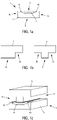
- FIG. 1a represents a microelectronic chip 1 (also referred to as a “chip” in the remainder of this description) comprising a microelectronic component, compatible with the assembly method in accordance with the invention.
- the microelectronic chip 1 comprises a substrate 3 comprising a microelectronic component 4, such as a transmission/reception circuit, a computing device, a sensor, an LED or any other form of integrated circuit produced on the substrate 3, for example using techniques known in the semiconductor field.
- the microelectronic component 4 is located on the upper face of the chip 1, called the first face 11 of the microelectronic chip 1.
- a protective layer is advantageously placed on the surface of the substrate 3.
- the lower face of chip 1 is called second face 12.
- the microelectronic component 4 can be electrically connected to one or a plurality of terminals of connection 4a leading to the first face 11 of the microelectronic chip 1, using conductive tracks or vias formed on or in the substrate 3. Alternatively, the connection terminals could be present on the second face 12 of the chip 1 .
- connection terminals 4a on their first face 11; recall that the presence of these connection terminals 4a is optional.
- the assembly method according to the invention makes it possible to assemble the microelectronic chip 1 with at least one wire element 7a, 7b.
- the assembly of the chip 1 with the wired element 7a, 7b can have a purely mechanical function: the wired element 7a, 7b then constitutes a mechanical support for the chip 1. In such a case, it is not not useful to provide one or more connection terminal(s) 4a on the first face 11 of the chip 1, the wired element 7a, 7b not being intended to establish electrical contact with the chip 1.
- the wired element 7a, 7b may be of any kind, in particular textile, polymer, metal, etc.
- connection terminals 4a of chip 1 and wire element 7a, 7b it may be advantageous for many applications to make electrical contact between connection terminals 4a of chip 1 and wire element 7a, 7b.
- the connection terminals 4a are advantageously placed on the first face 11 of the chip 1 and the wire element 7a, 7b is an electrical conductor.
- the microelectronic chip 1 can be assembled with two wired elements 7a, 7b, one of which is electrically conductive to establish electrical contact with a connection terminal 4a and the other of any kind to provide purely mechanical support. of chip 1.
- the wired element 7a, 7b can be of any type (subject to the scenarios stated above) insofar as it is sufficiently resistant to the mechanical and potentially chemical treatments to which it is likely to be exposed.
- the wire element 7a, 7b is a conductive electrical wire, as required by the invention, for example stainless steel or a copper-based alloy or copper.
- the wired element 7a, 7b may also be constituted by any type of conductive textile fibers.
- the assembly method comprises several steps, and in the first place a step of applying a removable cover 5 on a first face 11 of the microelectronic chip 1, the cover 5 being configured to form with the first face 11 at least one lateral temporary groove 2a, 2b, along at least one side face 1a, 1b of the microelectronic chip 1.
- the cover 5 comprises a contact face 51 intended to be applied to the first face 11 and having at least one shoulder 5a, 5b ( figure 1b ).
- This shoulder 5a, 5b makes it possible to form the temporary lateral groove 2a, 2b with the first face 11 of the microelectronic chip 1, when the cover 5 is applied thereto ( figure 1c ).
- the first face 11 is flat (or substantially flat after the manufacturing steps of the microelectronic component) and it is not necessary to create a specific groove.
- the contact face 51 of the cover 5, applied to the first face 11 has two shoulders 5a, 5b to form two grooves side temporary 2a, 2b parallel, with said first flat face 11 of the microelectronic chip 1.
- the contact face 51 of the cover 5 may include any number of shoulders, capable of forming temporary grooves, each arranged in any orientation, without departing from the scope of the invention.
- the geometric shape of the groove 2a, 2b is not limited to a generally parallelepipedal shape; indeed, the shoulder 5a, 5b of the cover 5 can have the shape of a slot ( figure 1b ) but also a bevel or have a concave rounded blank, which can generate a groove 2a, 2b of different shape.
- the cover 5 has a flat contact face 51 and the first face 11 of the microelectronic chip 1 has at least one shoulder 11a, to form the temporary lateral groove 2a with the flat contact face 51 of the cover 5.
- the terminal connection 4a can, in this embodiment, be made so as to open onto the first blank, in the plane of the first face 11, of the shoulder 11a (not shown) or onto the other substantially vertical blank of the shoulder 11a (as shown in figure 2b ).
- the first face 11 of the microelectronic chip 1 has two shoulders along each of its side faces 1a, 1b, to form two temporary side grooves 2a, 2b parallel, with the contact face 51 cover plane 5.
- first face 11 of the chip 1 may alternatively comprise any number of shoulders, capable of forming temporary grooves, each arranged in any orientation.
- cover 5 and chip 1 each comprise at least one shoulder to form at least one temporary lateral groove 2a, 2b when cover 5 is applied to first face 11 of chip 1 .
- the three embodiments exposed for the implementation of the method make it possible to relax the shape constraints of the microelectronic chip 1 to be assembled on the wire element 7a, 7b, because it is not necessary to form a specific groove on the chip itself.
- a chip 1 as it emerges from the manufacturing steps of the microelectronic component is compatible.
- a simple etching at the level of the first face 11 is required to create the shoulder.
- the step of applying the assembly method advantageously comprises maintaining contact between the contact face 51 of the cover 5 and the first face 11 of the chip 1, for example by vacuum.
- the cover 5 comprises at least one channel 52 capable of connecting its contact face 51 to a suction system 53 ( picture 3 ).
- the suction system 53 may for example include a vacuum pump.
- the invention is in no way limited to this mode of implementation, and any technique making it possible to maintain contact between the cover 5 and the chip 1 may be suitable.
- the cover 5 can be kept in contact with the first face 11 of chip 1 by the presence of a substance with low adhesive power on its contact face 51.
- the assembly method according to the present invention then comprises a step of inserting the wire element 7a, 7b into the temporary groove 2a, 2b, as illustrated in the figures 4a and 4b .
- a longitudinal portion of the wire element 7a, 7b is inserted into the temporary lateral groove 2a, 2b.
- the assembly method can include a second step of applying a support 20 to the second face 12 of the microelectronic chip 1, before the insertion step.
- the presence of the support 20 makes it possible to support and stiffen the chip 1, at least during the step of inserting the wired element 7a, 7b ( figure 4c ).
- the support 20 could for example be kept in contact with the second face 12 of the chip 1 by suction, or by the presence of a substance with low adhesive power, or even by the simple bearing pressure applied by the cover 5.
- the height and depth dimensions of the temporary grooves 2a, 2b which depend on the structural configuration of the cover 5 (first or third embodiment) and/or on the structural configuration of the chip 1 (second or third embodiment), are chosen large enough so that each wire element to be assembled can be housed in a temporary groove 2a, 2b without mechanically forcing its embedding. It is generally preferable, in order to promote the securing of the wire element 7a, 7b to the chip 1, that the longitudinal section of the wire element can be entirely housed in the grooves 2a, 2b, that is to say that the housed portion of each wire does not protrude from the side face 1a, 1b of the chip 1 at which the temporary groove 2a, 2b is located.
- the microelectronic chip 1 comprises at least one pad 6a, 6b on its first face 11, located in the area forming a first blank of the temporary groove 2a, 2b, when the cover 5 is applied to the first face 11.
- This pad 6a, 6b consisting of a connecting material, is intended to fix the wired element 7a, 7b on the chip 1, during the fixing step of the assembly method which will be described in the following description .
- the studs 6a, 6b are arranged over the entire length of the zone forming a first blank of each temporary groove 2a, 2b.
- the stud 6a, 6b may extend over at least part of the length of the first blank of the temporary lateral groove 2a, 2b.
- each stud 6a, 6b from a plurality of elementary studs, distinct from each other, arranged over a more or less extended length of the zone of the first face 11 forming a first blank of the temporary groove 2a ,2b.
- Each stud 6a, 6b forms a reserve of a bonding material which will allow the fixing on the chip 1 of the wire element 7a, 7b housed in a temporary groove 2a, 2b.
- the assembly of the chip 1 on the wired element 7a, 7b can only have a mechanical function.
- the connecting material forming the pads 6a, 6b can be a simple adhesive substance, for example made of polymer. It can be a viscous substance, which can be treated to harden during the next fixing step and thus ensure the connection between the wire element 7a, 7b and the chip 1.
- the pads 6a, 6b are advantageously deposited prior to the step of applying the cover 5 to the first face 11 of the chip 1.
- the connecting material of the pad 6a, 6b is chosen from electrically conductive materials. It can comprise a plurality of elemental compounds. It may for example be an alloy of metals, for example tin, silver and copper.
- the material constituting each stud 6a, 6b is chosen so that its melting temperature is relatively low. This melting temperature is lower than the maximum temperature to which the microelectronic component 4 of chip 1 can be exposed without being damaged. If, for example, this maximum temperature is 350°C, the material of the pads 6a, 6b will be chosen so that its melting temperature is less than 350°C, for example 300°C.
- this material is chosen so that its melting temperature is between 80°C and 100°C or 150°C, or 250°C. Furthermore, it is not necessary for all the studs 6a, 6b or all the elementary studs to be made of the same material.
- the pads 6a, 6b can be produced during the manufacture of the chip 1, for example by forming them by deposition on the substrate 3, in contact with the connection terminals 4a.
- the pads 6a, 6b are advantageously formed before the step of applying the cover 5 to the first face 11 of the chip 1.
- a longitudinal portion of at least one wire element 7a, 7b is placed along the (at least one) temporary groove 2a, 2b. Limited forces are then exerted on the wire element 7a, 7b to press it against the stud 6a, 6b.
- the assembly method according to the invention also comprises a step of fixing the wire element 7a, 7b to the microelectronic chip 1.
- the fixing step implements a bonding material or a substance adhesive making it possible to maintain contact between the wired element 7a, 7b and the chip 1, even when the temporary cover 5 is no longer in contact with the chip 1.
- the fixing step can be done by injecting an adhesive substance along the wire close to the first face 11 of the chip 1, after its insertion into the temporary groove 2a, 2b; the fixing step can also provide for the application of a bonding material, for example by soldering.
- the stud 6a, 6b has been formed beforehand in the groove 2a, 2b.
- the fixing step leads to the securing of all or part of the longitudinal portion of the wire element 7a, 7b inserted into the temporary groove 2a, 2b, on the first face 11 via the studs 6a, 6b.
- the pads 6a, 6b are formed by an adhesive substance that has not yet hardened, said substance will collapse during the insertion of the wire element 7a, 7b and partially surround it.
- the fixing step ends as soon as the adhesive substance has hardened so as to ensure the joining.
- This hardening may require treating the adhesive substance, for example by ultraviolet radiation.
- the material constituting the cover 5 or at least the material disposed on the surface of the cover 5 is chosen so that the adhesive substance does not adhere to it or hardly adheres to it, in order to avoid its joining to the cover 5, the latter being intended to be removed from the first face 11 of the chip 1.
- the fixing step comprises a sequence of localized heating near the temporary groove 2a, 2b, to melt the pad 6a ,6b against the wire element 7a,7b ( figure 6b ).
- the heating sequence can be implemented with a heating means, for example a flow generator of air or other heated fluid, by induction, or by light irradiation such as laser irradiation or ultra-light radiation. -violet, leading to the generation of a heat flux defining the heated zone at the level of chip 1.
- the heating can alternatively be obtained by thermal conduction, for example by raising the temperature of the cover 5 by means of heating resistors incorporated in the mass of this cover 5. In this case, the heating means is integrated into the cover 5 itself. .
- the studs 6a, 6b are brought to a treatment temperature higher than the melting temperature of the bonding material of which they are made, and for a time sufficient to melt it.
- the transition to the liquid state of the bonding material, combined with the modest holding forces against the temporary groove 2a, 2b, exerted on the wire element 7a, 7b leads to the partial coating of the latter in the temporary groove 2a, 2b as seen in the figure 6c .
- the wire element 7a, 7b is secured to the first face 11 and can make electrical contact with the connection terminals 4a of chip 1.
- the cover is formed, in this second case, of a material on which the conductive material of the pad 6a, 6b does not adhere in order to avoid adhesion of said pad 6a, 6b on the cover 5, which is intended, as as we have seen, to be removed from the first face 11 of chip 1.
- pad 6a, 6b, deposited and fixed on a connection terminal 4a of chip 1 may be composed of an alloy of metals, for example tin, silver and copper.
- the fixing step allows the attachment of the wire element 7a, 7b, for example consisting of a stainless steel, an alloy based copper or copper, on the pad 6a, 6b.
- the cover 5 may be composed of a type of ceramic, silicon oxide, a metal oxide or metal alloy, for example coated with chromium, material on which the solder (conductive material of the pad 6a, 6b) based on pewter does not adhere.
- the fixing step can be carried out successively or simultaneously for each of the wire elements 7a, 7b.
- the area exposed to the treatment temperature can be large enough to at least partially encompass all the pads 6a, 6b.
- the insertion step can comprise the exposure of several distinct zones, simultaneously or successively, each encompassing at least part of the pads 6a, 6b.
- the assembly method according to the invention finally comprises a step of removing the cover 5 of the microelectronic chip 1 ( figure 6d ), after the fixing step which has just been described.
- the contact face 51 is then separated from the first face 11 of the chip 1.
- the removal step can include interrupting the depressurization of the channels 52, which causes the contact to cease by suction between the contact face 51 and the first face 1.
- Cover 5 can be attached to the end of an articulated arm of a chip handling device such as an automatic “Pick and Place” machine according to English terminology.
- the articulated arm provided with a suction nozzle can pick up a chip 1 in a storage area and place it precisely in an assembly position, for example on a support 20, to successively carry out the steps of application then of removal of the cover 5 vis-à-vis the first face 11.
- the present invention takes advantage of the respective configurations of the cover 5 and of the microelectronic chip 1 to form at least one temporary groove 2a, 2b in which a wire element 7a, 7b can be easily and precisely positioned.
- the fixing of the wired element 7a, 7b on the chip 1, for example by means of a pad 6a, 6b arranged on the first face 11 of the chip 1, allows the joining and the mechanical strength of the assembly chip / wire.
- the cover 5 can then be removed from the chip 1 and be applied to another chip 1.
- the method according to the invention can be repeated and allow the assembly of a plurality of microelectronic chips 1 on at least one wired element 7a, 7b, to form a chain of chips 1.
- the assembly method according to the invention proposes a solution relaxing the constraints on the shape of the chip (and in particular on the presence of grooves) and allowing precise and reliable fixing of the wire element 7a, 7b on the chip 1 , due to the presence of the temporary groove 2a, 2b.
- the assembly method according to the invention may also comprise additional steps, after the wired element(s) 7a, 7b have been assembled to the chip 1 and the cover 5 removed.
- the method can provide for a step of strengthening the assembly formed by the chip 1 and the wired element(s) 7a, 7b.
- the reinforcement step can comprise the dispensing of an adhesive 18 at least on a part of the wired element fixed on the microelectronic chip 1, as illustrated on the figure 7a .
- the dispensing of the adhesive 18 can be completed by its polymerization, for example by UV treatment, which can be of a very short duration, of the order of a second or a few seconds, to stiffen the adhesive and promote its bonding to the elements with which it is in contact.
- the method can also comprise, as a complementary step, a step of encapsulating the microelectronic chip 1 and the longitudinal portion of the wired element 7a, 7b fixed on said chip, in a material 19 that is sufficiently rigid and impermeable, such as resin, making it possible to protect the assembled assembly from mechanical or chemical stresses in its final application ( figure 7b ).
- this encapsulation is such that all the faces of the chip 1 are well covered with the encapsulating material.
- the encapsulation step can be done with or without a prior reinforcement step.
- the method can also comprise, as an additional step, a step of cutting the wire element 7a, 7b.
- a step of cutting the wire element 7a, 7b This may involve taking a segment of the chain, with a view to integrating it into an object. It may also be a question of cutting out a portion of the wire element 7a, 7b in order to form a dipole antenna connected to a chip 1 constituting a transmission-reception circuit as is taught in the document US8471773 .
- the wire element 7a, 7b can be cut by any means known per se, for example using a mechanical shearing tool or by laser cutting.
Description
La présente invention concerne un procédé d'assemblage d'une puce microélectronique sur un élément filaire. Elle trouve un exemple d'application dans le domaine de l'étiquetage électronique RFID (« Radiofrequency Identification » selon la terminologie anglo-saxonne) pour associer directement une antenne à une puce d'émission-réception et fournir un dispositif radiofréquence particulièrement petit en taille et simple de fabrication. Ce dispositif peut être intégré dans un fil textile et ce fil lui-même intégré à une grande variété d'objets pour leurs identifications, leurs suivis, et leurs administrations. Plus généralement, elle peut trouver son application dans tous les domaines pouvant bénéficier de l'intégration d'une puce électronique, tel qu'un capteur, un actionneur, une diode électroluminescente, ou une cellule solaire à un élément filaire tel qu'un fil textile ou un fil conducteur en vue de son intégration dans un objet.The present invention relates to a method for assembling a microelectronic chip on a wire element. It finds an example of application in the field of RFID electronic labeling ("Radiofrequency Identification" according to the Anglo-Saxon terminology) to directly associate an antenna with a transmission-reception chip and to provide a radiofrequency device which is particularly small in size. and easy to manufacture. This device can be integrated into a textile thread and this thread itself integrated into a wide variety of objects for their identification, their monitoring, and their administration. More generally, it can find its application in all fields that can benefit from the integration of an electronic chip, such as a sensor, an actuator, a light-emitting diode, or a solar cell with a wired element such as a wire textile or a conductive yarn with a view to its integration into an object.
Dans certains cas, la puce électronique pourra être connectée électriquement au fil lui-même conducteur électrique. Dans d'autres cas, le fil conducteur électrique pourra être couplé par induction à une inductance logée dans la puce électronique, sans contact électrique direct entre la puce et le fil. Dans un exemple ne faisant pas partie de l'invention, au moins un fil peut être de nature variée (pas nécessairement conducteur électrique) pourra assurer le maintien mécanique de la puce électronique comprenant un composant autonome (par exemple autoalimenté par une micro-capacité intégrée à ladite puce).In some cases, the electronic chip may be electrically connected to the wire, which is itself an electrical conductor. In other cases, the electrical conductor wire may be coupled by induction to an inductor housed in the electronic chip, without direct electrical contact between the chip and the wire. In an example not forming part of the invention, at least one wire can be of various nature (not necessarily electrically conductive) can ensure the mechanical maintenance of the electronic chip comprising an autonomous component (for example self-powered by an integrated microcapacitor to said chip).
On connaît par exemple des documents
Selon cette technologie, la puce est munie d'une rainure latérale et on insère une section longitudinale du fil dans cette rainure. L'assemblage peut être obtenu par encastrement du fil dans la rainure, les dimensions du fil et de la rainure étant alors suffisamment ajustées pour solidariser mécaniquement les deux éléments l'un à l'autre. L'assemblage peut également être obtenu ou renforcé par l'ajout d'une matière adhésive entre le fil et la puce, ou par soudure ou brasage du fil et de la puce.According to this technology, the chip is provided with a lateral groove and a longitudinal section of the wire is inserted into this groove. The assembly can be obtained by embedding the wire in the groove, the dimensions of the wire and of the groove then being sufficiently adjusted to mechanically fasten the two elements to one another. The assembly can also be obtained or reinforced by adding an adhesive material between the wire and the chip, or by soldering or soldering the wire and the chip.
Dans le document
Les documents
La formation de rainures par assemblage ou par gravure sur les faces latérales d'une puce est une opération délicate mais également contraignante en terme de configuration structurelle de la puce. Pour autant, l'absence de rainures au niveau de la puce rend difficile le positionnement précis des fils et leur assemblage fiable sur la puce, notamment dans un contexte industriel où il est nécessaire de tenir une cadence de fabrication importante.The formation of grooves by assembly or by etching on the side faces of a chip is a delicate operation but also restrictive in terms of the structural configuration of the chip. However, the absence of grooves at the chip level makes it difficult to precisely position the wires and to assemble them reliably on the chip, in particular in an industrial context where it is necessary to maintain a high manufacturing rate.
Un objet de la présente invention est de proposer une solution obviant tout ou partie des inconvénients de l'état de l'art. Un objet de l'invention est notamment de proposer un procédé d'assemblage d'une puce microélectronique sur un élément filaire, relaxant les contraintes sur la forme de la puce et permettant une fixation précise et fiable de l'élément filaire sur ladite puce.An object of the present invention is to propose a solution obviating all or part of the drawbacks of the state of the art. An object of the invention is in particular to propose a method for assembling a microelectronic chip on a wire element, relaxing the constraints on the shape of the chip and allowing precise and reliable fixing of the wire element on said chip.
En vue de la réalisation de l'un de ces buts, l'objet de l'invention propose un procédé d'assemblage d'une puce microélectronique sur au moins un élément filaire conducteur électrique ; le procédé d'assemblage comprend :
- Une première étape d'application d'un capot sur une première face de la puce microélectronique, le capot étant configuré pour former avec la première face au moins une rainure temporaire latérale ;
- Une étape d'insertion de l'élément filaire dans la rainure temporaire ;
- Une étape de fixation de l'élément filaire sur la puce microélectronique ;
- Une étape de retrait du capot de la puce microélectronique.
- A first step of applying a cover to a first face of the microelectronic chip, the cover being configured to form with the first face at least one temporary lateral groove;
- A step of inserting the wire element into the temporary groove;
- A step of fixing the wire element to the microelectronic chip;
- A step for removing the microelectronic chip cover.
Selon d'autres caractéristiques avantageuses et non limitatives de l'invention, prises seules ou selon toute combinaison techniquement réalisable :
- le capot comporte une face de contact appliquée sur la première face de la puce microélectronique et présentant au moins un épaulement pour former la rainure temporaire latérale avec ladite première face ;
- la face de contact appliquée sur la première face présente deux épaulements pour former deux rainures temporaires latérales parallèles, avec ladite première face ;
- la première face de la puce microélectronique présente au moins un épaulement, pour former la rainure temporaire latérale avec une face de contact du capot ;
- la première face de la puce microélectronique présente deux épaulements, pour former deux rainures temporaires latérales parallèles, avec la face de contact du capot ;
- la première étape d'application du capot sur la première face de la puce microélectronique comprend un maintien en contact entre la face de contact du capot et ladite première face, par dépression ;
- lors de l'étape d'insertion, une portion longitudinale de l'élément filaire est insérée au moins en partie dans la rainure temporaire latérale ;
- le procédé d'assemblage comprend une deuxième étape d'application d'un support sur une deuxième face de la puce microélectronique, pour rigidifier ladite puce microélectronique au moins pendant l'étape d'insertion de l'élément filaire ;
- la puce microélectronique comprend au moins un plot sur sa première face, localisé dans la zone formant un premier flan de la rainure temporaire quand le capot est appliqué sur la première face ;
- l'étape de fixation s'opère entre l'élément filaire et le plot ;
- le capot est formé en un matériau sur lequel le matériau dont est formé le plot n'adhère pas ;
- l'élément filaire et le plot comprennent au moins un matériau conducteur électrique ;
- l'étape de fixation comprend une séquence de chauffage localisé à proximité de la rainure temporaire, pour faire fondre le plot contre l'élément filaire ;
- le capot comprend un moyen de chauffage pour la mise en œuvre de la séquence de chauffage ;
- le capot est fixé à l'extrémité d'un bras articulé d'un dispositif de manipulation de puce ;
- le procédé d'assemblage comprend, après l'étape de retrait du capot, une étape de renforcement comportant la dispense d'un adhésif au moins sur une partie de l'élément filaire fixé sur la puce microélectronique ;
- le procédé d'assemblage comprend, après l'étape de retrait du capot, une étape d'encapsulation de la puce microélectronique et au moins de la portion longitudinale de l'élément filaire fixée sur ladite puce.
- the cover comprises a contact face applied to the first face of the microelectronic chip and presenting at least one shoulder to form the temporary lateral groove with said first face;
- the contact face applied to the first face has two shoulders to form two parallel lateral temporary grooves, with said first face;
- the first face of the microelectronic chip has at least one shoulder, to form the temporary lateral groove with a contact face of the cover;
- the first face of the microelectronic chip has two shoulders, to form two parallel lateral temporary grooves, with the contact face of the cover;
- the first step of applying the cover to the first face of the microelectronic chip comprises maintaining contact between the contact face of the cover and said first face, by vacuum;
- during the insertion step, a longitudinal portion of the wire element is inserted at least partially into the temporary lateral groove;
- the assembly method comprises a second step of applying a support to a second face of the microelectronic chip, to stiffen said microelectronic chip at least during the step of inserting the wire element;
- the microelectronic chip comprises at least one pad on its first face, located in the area forming a first blank of the temporary groove when the cover is applied to the first face;
- the fixing step takes place between the wire element and the pad;
- the cover is formed from a material on which the material from which the pad is formed does not adhere;
- the wire element and the stud comprise at least one electrically conductive material;
- the fixing step comprises a sequence of localized heating near the temporary groove, to melt the stud against the wire element;
- the cover comprises a heating means for the implementation of the heating sequence;
- the cover is attached to the end of an articulated arm of a chip handling device;
- the assembly method comprises, after the step of removing the cover, a reinforcing step comprising the dispensing of an adhesive at least on a part of the wire element fixed on the microelectronic chip;
- the assembly method comprises, after the step of removing the cover, a step of encapsulating the microelectronic chip and at least the longitudinal portion of the wire element fixed on said chip.
D'autres caractéristiques et avantages de l'invention ressortiront de la description détaillée qui va suivre en référence aux figures annexées. Les figures sont des représentations schématiques qui, dans un objectif de lisibilité, ne sont pas nécessairement à l'échelle.
- la figure la présente une puce microélectronique compatible avec le procédé d'assemblage conforme à l'invention ;
- la
figure 1b présente des capots amovibles, selon un premier mode de réalisation, compatibles avec le procédé d'assemblage conforme à l'invention ; - la
figure 1c présente une étape d'application d'un capot sur une puce microélectronique, du procédé d'assemblage conforme à l'invention ; - la
figure 2a présente une autre puce microélectronique et un capot amovible, selon un deuxième mode de réalisation, compatible avec le procédé d'assemblage conforme à l'invention ; - la
figure 2b présente une étape d'application d'un capot sur une puce microélectronique, du procédé d'assemblage conforme à l'invention ; - la
figure 3 présente une étape d'application d'un capot sur une puce microélectronique, du procédé d'assemblage conforme à l'invention ; - les
figures 4a et 4b présentent une étape d'insertion d'un élément filaire dans une rainure temporaire, du procédé d'assemblage conforme à l'invention, respectivement en vue en coupe et en perspective ; - la
figure 4c présente une étape d'insertion d'un élément filaire dans une rainure temporaire, du procédé d'assemblage conforme à l'invention ; - la
figure 5 présente une étape d'application d'un capot sur une puce microélectronique, du procédé d'assemblage conforme à l'invention ; - les
figures 6a, 6b et 6c présentent des variantes de l'étape de fixation d'au moins un élément filaire sur une puce microélectronique, du procédé d'assemblage conforme à l'invention ; - la
figure 6d présente une étape de retrait d'un capot, du procédé d'assemblage conforme à l'invention ; - les
figures présentent des étapes complémentaires respectivement de renforcement et d'encapsulation d'un ensemble puce et élément filaire assemblé.7a et 7b
- FIG. 1a shows a microelectronic chip compatible with the assembly method according to the invention;
- the
figure 1b has removable covers, according to a first embodiment, compatible with the assembly method according to the invention; - the
figure 1c presents a step of applying a cover to a microelectronic chip, of the assembly method in accordance with the invention; - the
figure 2a presents another microelectronic chip and a removable cover, according to a second embodiment, compatible with the assembly method according to the invention; - the
figure 2b presents a step of applying a cover to a microelectronic chip, of the assembly method in accordance with the invention; - the
picture 3 - them
figures 4a and 4b present a step of inserting a wire element into a temporary groove, of the assembly method according to the invention, respectively in sectional view and in perspective; - the
figure 4c presents a step of inserting a wire element into a temporary groove, of the assembly method according to the invention; - the
figure 5 presents a step of applying a cover to a microelectronic chip, of the assembly method in accordance with the invention; - them
figures 6a, 6b and 6c present variants of the step of fixing at least one wire element on a microelectronic chip, of the assembly method in accordance with the invention; - the
figure 6d presents a step for removing a cover from the assembly method according to the invention; - them
figures 7a and 7b present complementary steps respectively of reinforcement and encapsulation of a chip assembly and assembled wire element.
Par souci de clarté, seules les étapes et éléments utiles à la compréhension de l'invention ont été représentés et seront décrits. En particulier, les composants (d'émission-réception radiofréquences, par exemple) élaborés sur les puces microélectroniques n'ont pas été détaillés, l'invention étant compatible avec les dispositifs usuels (capteurs de mesure, identifiants d'objets, par exemple), en fonction de l'application visée. Les étapes de fabrication collectives des puces microélectroniques sur un substrat n'ont pas non plus été détaillées, l'invention étant là encore compatible avec des puces microélectroniques élaborées avec les techniques usuelles.For the sake of clarity, only the steps and elements useful for understanding the invention have been shown and will be described. In particular, the components (for radiofrequency transmission-reception, for example) developed on the microelectronic chips have not been detailed, the invention being compatible with the usual devices (measurement sensors, object identifiers, for example) , depending on the intended application. The collective manufacturing steps of the microelectronic chips on a substrate have not been detailed either, the invention being here again compatible with microelectronic chips developed with the usual techniques.
La figure la représente une puce microélectronique 1 (également désignée « puce » dans la suite de cette description) comprenant un composant microélectronique, compatible avec le procédé d'assemblage conforme à l'invention.FIG. 1a represents a microelectronic chip 1 (also referred to as a “chip” in the remainder of this description) comprising a microelectronic component, compatible with the assembly method in accordance with the invention.
La puce microélectronique 1 comprend un substrat 3 comportant un composant microélectronique 4, tel qu'un circuit d'émission réception, un dispositif de calcul, un capteur, une LED ou tout autre forme de circuit intégré réalisé sur le substrat 3, par exemple à l'aide de techniques connues dans le domaine du semi-conducteur. Le composant microélectronique 4 se trouve sur la face supérieure de la puce 1, appelée première face 11 de la puce microélectronique 1. Pour protéger le composant microélectronique 4, une couche de protection est avantageusement disposée sur la surface du substrat 3.The
La face inférieure de la puce 1 est appelée deuxième face 12.The lower face of
Le composant microélectronique 4 peut être électriquement relié à une ou une pluralité de bornes de connexion 4a débouchant sur la première face 11 de la puce microélectronique 1, à l'aide de pistes ou de vias conducteurs formés sur ou dans le substrat 3. Alternativement, les bornes de connexion pourraient être présentes sur la deuxième face 12 de la puce 1.The
Les figures, par souci de simplicité, représentent des puces 1 comportant deux bornes de connexion 4a sur leur première face 11 ; rappelons que la présence de ces bornes de connexion 4a est optionnelle.The figures, for the sake of simplicity, represent
Le procédé d'assemblage selon l'invention permet d'assembler la puce microélectronique 1 avec au moins un élément filaire 7a,7b.The assembly method according to the invention makes it possible to assemble the
L'assemblage de la puce 1 avec l'élément filaire 7a,7b peut avoir une fonction uniquement mécanique : l'élément filaire 7a,7b constitue alors un support mécanique pour la puce 1. Dans un tel cas de figure, il n'est pas utile de prévoir une ou des borne (s) de connexion 4a sur la première face 11 de la puce 1, l'élément filaire 7a,7b n'ayant pas vocation à établir un contact électrique avec la puce 1. L'élément filaire 7a,7b pourra être de nature quelconque, notamment textile, polymère, métallique, etc.The assembly of the
Alternativement, il peut être avantageux pour de nombreuses applications, de réaliser un contact électrique entre les bornes de connexion 4a de la puce 1 et l'élément filaire 7a,7b. Dans ce cas de figure, les bornes de connexion 4a sont avantageusement placées sur la première face 11 de la puce 1 et l'élément filaire 7a,7b est un conducteur électrique.Alternatively, it may be advantageous for many applications to make electrical contact between
Selon encore une autre alternative, la puce microélectronique 1 peut être assemblée à deux éléments filaires 7a,7b, l'un conducteur électrique pour établir un contact électrique avec une borne de connexion 4a et l'autre de nature quelconque pour assurer un support uniquement mécanique de la puce 1.According to yet another alternative, the
L'élément filaire 7a,7b peut être de nature quelconque (sous réserve des cas de figure énoncés ci-dessus) dans la mesure où il est suffisamment résistant aux traitements mécaniques et potentiellement chimiques auxquels il est susceptible d'être exposé.The
Notamment dans le cas de figure dans lequel on souhaite mettre en liaison électrique le fil avec une borne 4a du composant microélectronique 4 de la puce 1, l'élément filaire 7a,7b est un fil électrique conducteur, comme l'exige l'invention, par exemple en acier inoxydable ou en un alliage à base de cuivre ou en cuivre. L'élément filaire 7a,7b pourra encore être constitué par tout type de fibres textiles conductrices.In particular in the case in which it is desired to electrically connect the wire with a terminal 4a of the
Le procédé d'assemblage comprend plusieurs étapes, et en premier lieu une étape d'application d'un capot 5 amovible sur une première face 11 de la puce microélectronique 1, le capot 5 étant configuré pour former avec la première face 11 au moins une rainure temporaire latérale 2a,2b, le long d'au moins une face latérale la, 1b de la puce microélectronique 1.The assembly method comprises several steps, and in the first place a step of applying a
Selon un premier mode de réalisation, le capot 5 comporte une face de contact 51 destinée à être appliquée sur la première face 11 et présentant au moins un épaulement 5a,5b (
Bien sur, la face de contact 51 du capot 5 pourra comporter un nombre quelconque d'épaulements, aptes à former des rainures temporaires, chacune disposée selon une orientation quelconque, sans sortir du cadre de l'invention.Of course, the
La forme géométrique de la rainure 2a,2b n'est pas limitée à une forme générale parallélépipédique ; en effet, l'épaulement 5a,5b du capot 5 peut avoir la forme d'un créneau (
Selon un deuxième mode de réalisation de l'invention, illustré sur les
Selon une variante avantageuse (non représentée), la première face 11 de la puce microélectronique 1 présente deux épaulements le long de chacune de ses faces latérales 1a,1b, pour former deux rainures temporaires latérales 2a,2b parallèles, avec la face de contact 51 plane du capot 5.According to an advantageous variant (not shown), the
Bien sur, la première face 11 de la puce 1 pourra alternativement comporter un nombre quelconque d'épaulements, aptes à former des rainures temporaires, chacune disposée selon une orientation quelconque.Of course, the
Selon un troisième mode de réalisation (non représenté), le capot 5 et la puce 1 comportent chacun au moins un épaulement pour former au moins une rainure temporaire latérale 2a,2b lorsque le capot 5 est appliqué sur la première face 11 de la puce 1.According to a third embodiment (not shown),
Les trois modes de réalisation exposés pour la mise en œuvre du procédé permettent de relaxer les contraintes de forme de la puce microélectronique 1 à assembler sur l'élément filaire 7a,7b, car il n'est pas nécessaire de former une rainure spécifique sur la puce elle-même. Selon le premier mode de réalisation, une puce 1 telle que sortie des étapes de fabrication du composant microélectronique est compatible. Selon les deuxième et troisième modes de réalisation, une gravure simple au niveau de la première face 11 est requise pour créer l'épaulement.The three embodiments exposed for the implementation of the method make it possible to relax the shape constraints of the
Dans la suite de la description et des figures, nous nous placerons dans le premier mode de réalisation énoncé. Les caractéristiques qui vont être exposées peuvent néanmoins s'appliquer à tous les modes de réalisation du procédé selon la présente invention.In the rest of the description and the figures, we will place ourselves in the first embodiment stated. The characteristics which will be explained can nevertheless be applied to all the embodiments of the method according to the present invention.
L'étape d'application du procédé d'assemblage comprend avantageusement le maintien en contact entre la face de contact 51 du capot 5 et la première face 11 de la puce 1, par exemple par dépression. Pour cela, le capot 5 comprend au moins un canal 52 apte à relier sa face de contact 51 à un système d'aspiration 53 (
Le procédé d'assemblage selon la présente invention comprend ensuite une étape d'insertion de l'élément filaire 7a,7b dans la rainure temporaire 2a,2b, comme illustré sur les
Optionnellement, le procédé d'assemblage peut comprendre une deuxième étape d'application d'un support 20 sur la deuxième face 12 de la puce microélectronique 1, avant l'étape d'insertion. La présence du support 20 permet de soutenir et rigidifier la puce 1, au moins pendant l'étape d'insertion de l'élément filaire 7a,7b (
Selon l'invention, les dimensions en hauteur et en profondeur des rainures temporaires 2a, 2b, qui dépendent de la configuration structurelle du capot 5 (premier ou troisième mode de réalisation) et/ou de la configuration structurelle de la puce 1 (deuxième ou troisième mode de réalisation), sont choisies suffisamment grandes pour que chaque élément filaire à assembler puisse être logé dans une rainure temporaire 2a, 2b sans mécaniquement forcer son encastrement. Il est généralement préférable, pour favoriser la solidarisation de l'élément filaire 7a,7b à la puce 1, que la section longitudinale de l'élément filaire puisse être entièrement logée dans les rainures 2a,2b, c'est-à-dire que la portion logée de chaque fil ne déborde pas de la face latérale 1a,1b de la puce 1 au niveau de laquelle se trouve la rainure temporaire 2a,2b.According to the invention, the height and depth dimensions of the
Lorsque une pluralité de rainures temporaires 2a, 2b, sont présentes, celles-ci ne sont pas nécessairement de mêmes dimensions. Similairement, les éléments filaires 7a,7b destinés à être logés dans les rainures temporaires 2a,2b ne sont pas nécessairement de même nature et ne présentent pas nécessairement des sections transversales de dimensions identiques.When a plurality of
Avantageusement, la puce microélectronique 1 comprend au moins un plot 6a, 6b sur sa première face 11, localisé dans la zone formant un premier flan de la rainure temporaire 2a,2b, quand le capot 5 est appliqué sur la première face 11. Ce plot 6a,6b, constitué d'un matériau de liaison, est destiné à fixer l'élément filaire 7a,7b sur la puce 1, lors de l'étape de fixation du procédé d'assemblage qui va être décrite dans la suite de la description.Advantageously, the
Dans l'exemple représenté sur la
On pourra également choisir de constituer chaque plot 6a, 6b d'une pluralité de plots élémentaires, distincts les uns des autres, disposés sur une longueur plus ou moins étendue de la zone de la première face 11 formant un premier flan de la rainure temporaire 2a,2b.It is also possible to choose to form each
Quelle que soient la forme, le volume, la disposition occupée par les plots 6a, 6b dans les rainures temporaires 2a, 2b, ceux-ci présentent avantageusement une dimension telle, qu'en leur présence il n'est pas possible de loger les éléments filaires dans les rainures temporaires 2a, 2b sans que les fils entrent en contact avec les plots 6a,6b. Chaque plot 6a, 6b forme une réserve d'un matériau de liaison qui permettra la fixation sur la puce 1, de l'élément filaire 7a,7b logé dans une rainure temporaire 2a, 2b.Whatever the shape, the volume, the arrangement occupied by the
Comme énoncé précédemment, selon un premier cas de figure, l'assemblage de la puce 1 sur l'élément filaire 7a,7b peut n'avoir qu'une fonction mécanique. Dans ce cas, le matériau de liaison formant les plots 6a,6b peut être une simple substance adhésive par exemple en polymère. Il peut s'agir d'une substance visqueuse, qui peut être traitée pour durcir au cours de l'étape suivante de fixation et ainsi assurer la solidarisation entre l'élément filaire 7a,7b et la puce 1.As stated previously, according to a first scenario, the assembly of the
Les plots 6a, 6b sont avantageusement déposés préalablement à l'étape d'application du capot 5 sur la première face 11 de la puce 1.The
Selon un deuxième cas de figure, dans lequel on souhaite établir une connexion électrique entre la puce 1 et l'élément filaire 7a,7b, le matériau de liaison du plot 6a,6b est choisi parmi les matériaux conducteurs électriques. Il peut comprendre une pluralité de composés élémentaires. Il peut par exemple s'agir d'un alliage de métaux, par exemple d'étain, d'argent et de cuivre. Le matériau constituant chaque plot 6a, 6b est choisi pour que sa température de fusion soit relativement peu élevée. Cette température de fusion est inférieure à la température maximale à laquelle le composant microélectronique 4 de la puce 1 peut-être exposé sans être endommagé. Si, par exemple cette température maximale est de 350°C, on choisira le matériau des plots 6a, 6b pour que sa température de fusion soit inférieure à 350°C, par exemple 300°C. Avantageusement, pour des raisons de simplicité de mise en œuvre du procédé d'assemblage, ce matériau est choisi pour que sa température de fusion soit comprise entre 80°C et 100°C ou 150°C, ou 250°C. Par ailleurs, il n'est pas nécessaire que tous les plots 6a, 6b ou tous les plots élémentaires soient constitués du même matériau.According to a second scenario, in which it is desired to establish an electrical connection between the
Les plots 6a, 6b peuvent être élaborés au cours de la fabrication de la puce 1, par exemple en les formant par dépôt sur le substrat 3, en contact avec les bornes de connexions 4a. Les plots 6a,6b sont avantageusement formés avant l'étape d'application du capot 5 sur la première face 11 de la puce 1.The
Au cours de l'étape d'insertion, on dispose une portion longitudinale d'au moins un élément filaire 7a, 7b le long de la (au moins une) rainure temporaire 2a, 2b. On exerce alors des efforts limités sur l'élément filaire 7a, 7b pour le plaquer contre le plot 6a, 6b.During the insertion step, a longitudinal portion of at least one
Le procédé d'assemblage selon l'invention comprend également une étape de fixation de l'élément filaire 7a,7b sur la puce microélectronique 1. D'une manière générale, l'étape de fixation met en œuvre un matériau de liaison ou une substance adhésive permettant de maintenir le contact entre l'élément filaire 7a, 7b et la puce 1, même lorsque le capot temporaire 5 n'est plus en contact avec la puce 1.The assembly method according to the invention also comprises a step of fixing the
Ce matériau de liaison ou cette substance adhésive peut avoir été dispensé(e) avant l'application du capot 5 et l'insertion de l'élément filaire 7a,7b, comme précédemment énoncé, ou après ces étapes. Ainsi, l'étape de fixation peut se faire par injection d'une substance adhésive le long du fil à proximité de la première face 11 de la puce 1, après son insertion dans la rainure temporaire 2a,2b ; l'étape de fixation peut également prévoir l'application d'un matériau de liaison, par exemple par brasure.This bonding material or this adhesive substance may have been dispensed before the application of the
Dans le mode de mise en œuvre préféré, le plot 6a, 6b a été préalablement constitué dans la rainure 2a, 2b. Comme cela est présenté sur la
Dans le premier cas de figure où les plots 6a,6b sont formés par une substance adhésive non encore durcie, ladite substance va s'affaisser lors de l'insertion de l'élément filaire 7a,7b et l'entourer partiellement. L'étape de fixation aboutit dès que la substance adhésive a durci de manière à assurer la solidarisation. Ce durcissement peut nécessiter de traiter la substance adhésive, par exemple par un rayonnement ultra-violet.In the first case where the
Le matériau constituant le capot 5 ou tout au moins le matériau disposé à la surface du capot 5 est choisi de manière à ce que la substance adhésive n'y adhère pas ou peu, afin d'éviter sa solidarisation au capot 5, ce dernier étant destiné à être retiré de la première face 11 de la puce 1.The material constituting the
Dans le deuxième cas de figure où les plots 6a,6b sont formés par un matériau conducteur, par exemple métallique, l'étape de fixation comprend une séquence de chauffage localisé à proximité de la rainure temporaire 2a,2b, pour faire fondre le plot 6a,6b contre l'élément filaire 7a,7b (
La séquence de chauffage peut être mise en œuvre avec un moyen de chauffage, par exemple un générateur de flux d'air ou d'un autre fluide chauffé, par induction, ou par une irradiation lumineuse telle qu'une irradiation laser ou un rayonnement ultra-violet, conduisant à générer un flux de chaleur définissant la zone chauffée au niveau de la puce 1. Le chauffage peut alternativement être obtenu par conduction thermique, par exemple en portant en température le capot 5 par l'intermédiaire de résistances chauffantes incorporées dans la masse de ce capot 5. Dans ce cas, le moyen chauffage est intégré au capot 5 lui-même.The heating sequence can be implemented with a heating means, for example a flow generator of air or other heated fluid, by induction, or by light irradiation such as laser irradiation or ultra-light radiation. -violet, leading to the generation of a heat flux defining the heated zone at the level of
Ainsi, on porte les plots 6a, 6b à une température de traitement supérieure à la température de fusion du matériau de liaison les composant, et pendant une durée suffisante pour le faire fondre. Le passage à l'état liquide du matériau de liaison, combiné aux efforts modestes de maintien contre la rainure temporaire 2a,2b, exercés sur l'élément filaire 7a, 7b conduit à l'enrobage partiel de ce dernier dans la rainure temporaire 2a, 2b comme cela est visible sur la
La séquence de chauffage terminée, une température inférieure à la température de fusion du matériau de liaison est restaurée, typiquement la température ambiante, ce qui conduit à redonner au matériau de liaison une constitution solide : l'élément filaire 7a,7b est rendu solidaire de la première face 11 et peut établir un contact électrique avec les bornes de connexion 4a de la puce 1.Once the heating sequence is complete, a temperature below the melting point of the bonding material is restored, typically room temperature, which results in restoring the bonding material to a solid constitution: the
Le capot est formé, dans ce deuxième cas de figure, en un matériau sur lequel le matériau conducteur du plot 6a,6b n'adhère pas afin d'éviter une adhésion dudit plot 6a,6b sur le capot 5, lequel est destiné, comme on l'a vu, à être retiré de la première face 11 de la puce 1. A titre d'exemple, le plot 6a,6b, déposé et fixé sur une borne de connexion 4a de la puce 1, pourra être composé d'un alliage de métaux, par exemple d'étain, d'argent et de cuivre. L'étape de fixation permet la solidarisation de l'élément filaire 7a,7b, par exemple constitué d'un acier inoxydable, d'un alliage à base de cuivre ou de cuivre, sur le plot 6a,6b. Le capot 5 pourra être composé d'un type de céramique, d'oxyde de silicium, d'un oxyde métallique ou alliage métallique par exemple revêtu de chrome, matériau sur lequel la brasure (matériau conducteur du plot 6a,6b) à base d'étain n'adhère pas.The cover is formed, in this second case, of a material on which the conductive material of the
Lorsque la puce 1 présente plusieurs rainures temporaires 2a, 2b pour accueillir plusieurs éléments filaires 7a, 7b, l'étape de fixation peut être réalisée successivement ou simultanément pour chacun des éléments filaires 7a,7b. La zone exposée à la température de traitement peut être suffisamment large pour englober au moins en partie tous les plots 6a, 6b. Alternativement, l'étape d'insertion peut comprendre l'exposition de plusieurs zones distinctes, simultanément ou successivement, chacune englobant une partie au moins des plots 6a, 6b.When
Le procédé d'assemblage selon l'invention comprend enfin une étape de retrait du capot 5 de la puce microélectronique 1 (
Le capot 5 peut être fixé à l'extrémité d'un bras articulé d'un dispositif de manipulation de puce tel qu'une machine automatique de « Pick and Place » selon la terminologie anglo-saxonne. Le bras articulé muni d'une buse d'aspiration pourra saisir une puce 1 dans une zone de stockage et la placer avec précision dans une position d'assemblage, par exemple sur un support 20, pour successivement opérer les étapes d'application puis de retrait du capot 5 vis-à-vis de la première face 11.
La présente invention met à profit les configurations respectives du capot 5 et de la puce microélectronique 1 pour former au moins une rainure temporaire 2a,2b dans laquelle un élément filaire 7a,7b peut être facilement et précisément positionné. La fixation de l'élément filaire 7a,7b sur la puce 1, par exemple par l'intermédiaire d'un plot 6a,6b disposé sur la première face 11 de la puce 1, permet la solidarisation et la tenue mécanique de l'ensemble puce / fil. Le capot 5 peut alors être retiré de la puce 1 et être appliqué sur une autre puce 1. Le procédé selon l'invention peut être répété et permettre l'assemblage d'une pluralité de puces microélectroniques 1 sur au moins un élément filaire 7a,7b, pour former une chaîne de puces 1.The present invention takes advantage of the respective configurations of the
Le procédé d'assemblage selon l'invention propose une solution relaxant les contraintes sur la forme de la puce (et en particulier sur la présence de rainures) et permettant une fixation précise et fiable de l'élément filaire 7a,7b sur la puce 1, du fait de la présence de la rainure temporaire 2a,2b.The assembly method according to the invention proposes a solution relaxing the constraints on the shape of the chip (and in particular on the presence of grooves) and allowing precise and reliable fixing of the
Le procédé d'assemblage selon l'invention peut également comprendre des étapes complémentaires, après que le (s) élément(s) filaire(s) 7a, 7b ai(en)t été assemblé(s) à la puce 1 et le capot 5 retiré.The assembly method according to the invention may also comprise additional steps, after the wired element(s) 7a, 7b have been assembled to the
Ainsi, le procédé peut prévoir une étape de renforcement de l'assemblage formé par la puce 1 et le (ou les) élément(s) filaire(s) 7a, 7b. L'étape de renforcement peut comprendre la dispense d'un adhésif 18 au moins sur une partie de l'élément filaire fixé sur la puce microélectronique 1, comme illustré sur le
Le procédé peut également comprendre, comme étape complémentaire, une étape d'encapsulation de la puce microélectronique 1 et de la portion longitudinale de l'élément filaire 7a,7b fixé sur ladite puce, dans un matériau 19 suffisamment rigide et étanche, comme de la résine, permettant de protéger l'ensemble assemblé des sollicitations mécaniques ou chimiques dans son application finale (
L'étape d'encapsulation peut être faite avec ou sans étape de renforcement préalable.The encapsulation step can be done with or without a prior reinforcement step.
Le procédé peut également comprendre comme étape complémentaire, une étape de découpe de l'élément filaire 7a, 7b. Il peut s'agir de prélever un segment de la chaine, en vue de son intégration dans un objet. Il peut également s'agir de découper une portion de l'élément filaire 7a, 7b afin de former une antenne dipôle reliée à une puce 1 constituant un circuit d'émission réception comme cela est enseigné dans le document
Bien entendu l'invention n'est pas limitée au mode de mise en œuvre décrit et on peut y apporter des variantes de réalisation sans sortir du cadre de l'invention tel que défini par les revendications.Of course, the invention is not limited to the mode of implementation described and variant embodiments can be added thereto without departing from the scope of the invention as defined by the claims.
Claims (15)
- Method for joining a microelectronic chip (1) to at least one electrically conductive wire element (7a, 7b); the joining method comprising:- a first step of applying a cover (5) to a first face (11) of the microelectronic chip (1), the cover (5) being configured to form at least one temporary side groove (2a, 2b) with the first face (11);- a step of inserting the wire element (7a, 7b) into the temporary groove (2a, 2b);- a step of attaching the wire element (7a, 7b) to the microelectronic chip (1);the joining method being characterized in that it subsequently comprises:- a step of removing the cover (5) from the microelectronic chip (1).
- Joining method according to the preceding claim, wherein the cover (5) comprises a contact face (51) which is applied to the first face (11) of the microelectronic chip (1) and has at least one shoulder (5a, 5b) for forming the temporary side groove (2a, 2b) with said first face (11).
- Joining method according to either of the preceding claims, wherein the first face (11) of the microelectronic chip (1) has at least one shoulder (11a) for forming the temporary side groove (2a) with a contact face (51) of the cover (5).
- Joining method according to either of the two preceding claims, wherein the first step of applying the cover (5) to the first face (11) of the microelectronic chip (1) comprises maintaining contact between the contact face (51) of the cover (5) and said first face (11) by negative pressure.
- Joining method according to any of the preceding claims, wherein, during the insertion step, a longitudinal portion of the wire element (7a, 7b) is inserted at least partially into the temporary side groove (2a, 2b).
- Joining method according to any of the preceding claims, comprising a second step of applying a support (20) to a second face (12) of the microelectronic chip (1) so as to stiffen said microelectronic chip (1) at least during the step of inserting the wire element (7a, 7b).
- Joining method according to any of the preceding claims, wherein the microelectronic chip (1) comprises at least one contact pad (6a, 6b) on its first face (11), which contact pad is located in the region which forms a first flank of the temporary groove (2a, 2b) when the cover (5) is applied to the first face (11).
- Joining method according to the preceding claim, wherein the attaching step takes place between the wire element (7a, 7b) and the contact pad (6a, 6b).
- Joining method according to either of the two preceding claims, wherein the cover (5) is formed from a material to which the material from which the contact pad (6a, 6b) is formed does not adhere.
- Joining method according to any of the three preceding claims, wherein the wire element (7a, 7b) and the contact pad (6a, 6b) comprise at least one electrically conductive material.
- Joining method according to any of the four preceding claims, wherein the attaching step comprises a sequence of localized heating near the temporary groove (2a, 2b) so as to melt the contact pad (6a, 6b) against the wire element (7a, 7b).
- Joining method according to the preceding claim, wherein the cover (5) comprises a heating means for implementing the heating sequence.
- Joining method according to any of the preceding claims, wherein the cover (5) is attached to the end of an articulated arm of a chip handling device.
- Joining method according to any of the preceding claims, comprising, after the step of removing the cover (5), a reinforcing step comprising dispensing an adhesive (18) at least on a part of the wire element (7a, 7b) which is attached to the microelectronic chip (1).
- Joining method according to any of the preceding claims, comprising, after the step of removing the cover (5), a step of encapsulating the microelectronic chip (1) and at least the longitudinal portion of the wire element (7a, 7b) attached to said chip (1).
Applications Claiming Priority (2)
| Application Number | Priority Date | Filing Date | Title |
|---|---|---|---|
| FR1753404A FR3065578B1 (en) | 2017-04-19 | 2017-04-19 | METHOD FOR ASSEMBLING A MICROELECTRONIC CHIP ON A WIRED ELEMENT |
| PCT/FR2018/050955 WO2018193198A1 (en) | 2017-04-19 | 2018-04-16 | Method for joining a microelectronic chip to a wire element |
Publications (2)
| Publication Number | Publication Date |
|---|---|
| EP3613074A1 EP3613074A1 (en) | 2020-02-26 |
| EP3613074B1 true EP3613074B1 (en) | 2022-06-22 |
Family
ID=59521013
Family Applications (1)
| Application Number | Title | Priority Date | Filing Date |
|---|---|---|---|
| EP18719983.1A Active EP3613074B1 (en) | 2017-04-19 | 2018-04-16 | Method for joining a microelectronic chip to a wire element |
Country Status (5)
| Country | Link |
|---|---|
| US (1) | US11081466B2 (en) |
| EP (1) | EP3613074B1 (en) |
| CN (1) | CN110520978B (en) |
| FR (1) | FR3065578B1 (en) |
| WO (1) | WO2018193198A1 (en) |
Families Citing this family (10)
| Publication number | Priority date | Publication date | Assignee | Title |
|---|---|---|---|---|
| US11443160B2 (en) | 2019-09-18 | 2022-09-13 | Sensormatic Electronics, LLC | Systems and methods for laser tuning and attaching RFID tags to products |
| US10783424B1 (en) | 2019-09-18 | 2020-09-22 | Sensormatic Electronics, LLC | Systems and methods for providing tags adapted to be incorporated with or in items |
| FR3103043B1 (en) | 2019-11-08 | 2022-08-05 | Primo1D | ELECTRONIC IDENTIFICATION TAG COMPRISING A WIRED ELECTRONIC IDENTIFICATION DEVICE, METHOD FOR MANUFACTURING SUCH A LABEL AND TEXTILE PART PROVIDED WITH SUCH A LABEL. |
| FR3103293B1 (en) * | 2019-11-19 | 2022-07-08 | Commissariat Energie Atomique | RFID Tag |
| US11055588B2 (en) | 2019-11-27 | 2021-07-06 | Sensormatic Electronics, LLC | Flexible water-resistant sensor tag |
| EP3923195B1 (en) | 2020-06-11 | 2023-08-23 | Primo1D | Electronic label with a flexible and deformable nature |
| FR3119944B1 (en) | 2021-02-15 | 2023-02-10 | Primo1D | Radiofrequency transmission-reception device using an antenna composed of a textile yarn and a conductive tape and associated electronic tag |
| US11755874B2 (en) | 2021-03-03 | 2023-09-12 | Sensormatic Electronics, LLC | Methods and systems for heat applied sensor tag |
| US11869324B2 (en) | 2021-12-23 | 2024-01-09 | Sensormatic Electronics, LLC | Securing a security tag into an article |
| FR3131253B1 (en) | 2021-12-23 | 2024-01-05 | Primo1D | Pneumatic equipped with a radio frequency transmission-reception device |
Citations (7)
| Publication number | Priority date | Publication date | Assignee | Title |
|---|---|---|---|---|
| WO2008080245A2 (en) * | 2006-12-28 | 2008-07-10 | Gerhard Staufert | Filament |
| WO2009112644A1 (en) * | 2008-03-06 | 2009-09-17 | Commissariat A L'energie Atomique | Assembly including a wire member and a microelectronic chip with a notch, including at least one stud for holding the wire member |
| EP2339618A2 (en) * | 2009-12-23 | 2011-06-29 | Commissariat à l'Énergie Atomique et aux Énergies Alternatives | Method for assembling at least one chip with a wired element, electronic chip with deformable connection element, method for manufacturing a plurality of chips and assembly of at least one chip with a wired element |
| EP2390194A1 (en) * | 2010-05-25 | 2011-11-30 | Commissariat à l'Énergie Atomique et aux Énergies Alternatives | Apparatus for assembling chip devices on wires |
| EP2429006A2 (en) * | 2010-09-09 | 2012-03-14 | Commissariat à l'Énergie Atomique et aux Énergies Alternatives | Method for manufacturing chip elements provided with wire insertion grooves |
| WO2014041107A1 (en) * | 2012-09-17 | 2014-03-20 | Commissariat A L'energie Atomique Et Aux Energies Alternatives | Cap for a chip device having a groove, device provided with said cap, assembly consisting of the device and a wire element, and manufacturing method thereof |
| EP2897084A1 (en) * | 2014-01-20 | 2015-07-22 | King's Metal Fiber Technologies Co., Ltd. | Structure of textile |
Family Cites Families (10)
| Publication number | Priority date | Publication date | Assignee | Title |
|---|---|---|---|---|
| US7023093B2 (en) * | 2002-10-24 | 2006-04-04 | International Business Machines Corporation | Very low effective dielectric constant interconnect Structures and methods for fabricating the same |
| DE102005055280B3 (en) * | 2005-11-17 | 2007-04-12 | Infineon Technologies Ag | Connecting elements for semiconductor components have mushroom shape with first metal area filling out indentations on top of insulating layer and with second metal area on containing refractory inter-metallic phases of metals of solder |
| JP4855849B2 (en) * | 2006-06-30 | 2012-01-18 | 富士通株式会社 | RFID tag manufacturing method and RFID tag |
| FR2905518B1 (en) | 2006-08-29 | 2008-12-26 | Commissariat Energie Atomique | LATERAL FACED MICROELECTRONIC CHIP WITH GROOVES AND METHOD OF MANUFACTURE |
| FR2917895B1 (en) | 2007-06-21 | 2010-04-09 | Commissariat Energie Atomique | METHOD FOR MANUFACTURING AN ASSEMBLY OF MECHANICALLY CONNECTED CHIPS USING A FLEXIBLE CONNECTION |
| JP5498751B2 (en) * | 2009-10-05 | 2014-05-21 | ルネサスエレクトロニクス株式会社 | Manufacturing method of semiconductor device |
| WO2011070240A1 (en) | 2009-12-09 | 2011-06-16 | Commissariat A L'energie Atomique Et Aux Energies Alternatives | Photovoltaic cell, method for assembling plurality of cells, and assembly of a plurality of photovoltaic cells |
| FR2960339B1 (en) * | 2010-05-18 | 2012-05-18 | Commissariat Energie Atomique | METHOD FOR PRODUCING CHIP ELEMENTS WITH WIRE INSERTION GROOVES |
| FR2961947B1 (en) | 2010-06-24 | 2013-03-15 | Commissariat Energie Atomique | INCORPORATION OF CHIP ELEMENTS IN A GUIPE WIRE |
| JP2013077631A (en) * | 2011-09-29 | 2013-04-25 | Ulvac Japan Ltd | Manufacturing method of semiconductor device and semiconductor device |
-
2017
- 2017-04-19 FR FR1753404A patent/FR3065578B1/en not_active Expired - Fee Related
-
2018
- 2018-04-16 WO PCT/FR2018/050955 patent/WO2018193198A1/en unknown
- 2018-04-16 EP EP18719983.1A patent/EP3613074B1/en active Active
- 2018-04-16 CN CN201880024863.9A patent/CN110520978B/en active Active
- 2018-04-16 US US16/606,684 patent/US11081466B2/en active Active
Patent Citations (7)
| Publication number | Priority date | Publication date | Assignee | Title |
|---|---|---|---|---|
| WO2008080245A2 (en) * | 2006-12-28 | 2008-07-10 | Gerhard Staufert | Filament |
| WO2009112644A1 (en) * | 2008-03-06 | 2009-09-17 | Commissariat A L'energie Atomique | Assembly including a wire member and a microelectronic chip with a notch, including at least one stud for holding the wire member |
| EP2339618A2 (en) * | 2009-12-23 | 2011-06-29 | Commissariat à l'Énergie Atomique et aux Énergies Alternatives | Method for assembling at least one chip with a wired element, electronic chip with deformable connection element, method for manufacturing a plurality of chips and assembly of at least one chip with a wired element |
| EP2390194A1 (en) * | 2010-05-25 | 2011-11-30 | Commissariat à l'Énergie Atomique et aux Énergies Alternatives | Apparatus for assembling chip devices on wires |
| EP2429006A2 (en) * | 2010-09-09 | 2012-03-14 | Commissariat à l'Énergie Atomique et aux Énergies Alternatives | Method for manufacturing chip elements provided with wire insertion grooves |
| WO2014041107A1 (en) * | 2012-09-17 | 2014-03-20 | Commissariat A L'energie Atomique Et Aux Energies Alternatives | Cap for a chip device having a groove, device provided with said cap, assembly consisting of the device and a wire element, and manufacturing method thereof |
| EP2897084A1 (en) * | 2014-01-20 | 2015-07-22 | King's Metal Fiber Technologies Co., Ltd. | Structure of textile |
Also Published As
| Publication number | Publication date |
|---|---|
| US20200335475A1 (en) | 2020-10-22 |
| US11081466B2 (en) | 2021-08-03 |
| FR3065578A1 (en) | 2018-10-26 |
| FR3065578B1 (en) | 2019-05-03 |
| WO2018193198A1 (en) | 2018-10-25 |
| EP3613074A1 (en) | 2020-02-26 |
| CN110520978A (en) | 2019-11-29 |
| CN110520978B (en) | 2023-08-15 |
Similar Documents
| Publication | Publication Date | Title |
|---|---|---|
| EP3613074B1 (en) | Method for joining a microelectronic chip to a wire element | |
| EP3574521B1 (en) | Method for inserting a wire into a groove of a semiconductor chip, and piece of equipment for implementing such a method | |
| EP2339618B1 (en) | Method for assembling at least one chip with a wired element, electronic chip with deformable connection element, method for manufacturing a plurality of chips and assembly of at least one chip with a wired element | |
| EP0128822B1 (en) | Method of producing memory cards, and cards obtained thereby | |
| EP2649566B1 (en) | Electronic card having an external connector | |
| EP2737781B1 (en) | Method for assembling microelectronic-chip device in fabric, chip device, and fabric containing a crimped chip device | |
| FR2917895A1 (en) | METHOD FOR MANUFACTURING AN ASSEMBLY OF MECHANICALLY CONNECTED CHIPS USING A FLEXIBLE CONNECTION | |
| FR2705832A1 (en) | A method of producing a sealing bead and mechanical strength between a substrate and a chip hybridized by beads on the substrate. | |
| EP2057687A1 (en) | Bare microelectronic chip provided with a recess forming a housing for a wire element constituting a flexible mechanical support, fabrication process and microstructure | |
| WO2021099713A1 (en) | Method for manufacturing a functional chip suitable for being assembled to wire elements | |
| EP2807681B1 (en) | Method for producing a microelectronic device comprising a plurality of wire light-emitting diodes and corresponding set of multilayer assemblies | |
| WO2014147355A1 (en) | Flip-chip assembly process comprising pre-coating interconnect elements | |
| EP2002384B1 (en) | Radiofrequency device | |
| EP1192592B1 (en) | Device and method for making devices comprising at least a chip fixed on a support | |
| EP1427008B1 (en) | Process of manufacturing an electronic module comprising an active component on a substrate | |
| WO2000077731A1 (en) | Device and method for making devices comprising at least a chip mounted on a support | |
| EP3171395B1 (en) | Formation of interconnections by curving conductive elements under a microelectronic device such as a chip | |
| EP3571718A1 (en) | Method for manufacturing an electronic device, and electronic device | |
| FR2781068A1 (en) | PROCESS FOR MANUFACTURING A MICROCIRCUIT CARD ALLOWING TO LIMIT THE MECHANICAL CONSTRAINTS TRANSMITTED TO THIS CARD AND THUS OBTAINED CARD | |
| EP2009697B1 (en) | Fabrication process of a matrix-shaped radiation detector and process for exchanging single detection modules of this matrix | |
| WO1997042657A1 (en) | Electric component in integrated circuit form for hot insertion in a substrate and methods for manufacturing same | |
| FR2833754A1 (en) | Production of electronic component uses film handle fixed permanently to rear surface of semiconductor wafer for manipulating it | |
| WO2008107274A1 (en) | Process for manufacturing a device comprising an integrated circuit and an antenna coil connected to it | |
| FR2906644A1 (en) | Optoelectronic and/or electronic circuits connecting device for optical fiber telecommunication field, has conductive tracks provided with respect to junction line, on circuits, and conductive bridge provided between tracks |
Legal Events
| Date | Code | Title | Description |
|---|---|---|---|
| STAA | Information on the status of an ep patent application or granted ep patent |
Free format text: STATUS: UNKNOWN |
|
| STAA | Information on the status of an ep patent application or granted ep patent |
Free format text: STATUS: THE INTERNATIONAL PUBLICATION HAS BEEN MADE |
|
| PUAI | Public reference made under article 153(3) epc to a published international application that has entered the european phase |
Free format text: ORIGINAL CODE: 0009012 |
|
| STAA | Information on the status of an ep patent application or granted ep patent |
Free format text: STATUS: REQUEST FOR EXAMINATION WAS MADE |
|
| 17P | Request for examination filed |
Effective date: 20190919 |
|
| AK | Designated contracting states |
Kind code of ref document: A1 Designated state(s): AL AT BE BG CH CY CZ DE DK EE ES FI FR GB GR HR HU IE IS IT LI LT LU LV MC MK MT NL NO PL PT RO RS SE SI SK SM TR |
|
| AX | Request for extension of the european patent |
Extension state: BA ME |
|
| RIN1 | Information on inventor provided before grant (corrected) |
Inventor name: MACKANIC, CHRISTOPHER Inventor name: ROLLAND, DELPHINE Inventor name: ARENE, EMMANUEL Inventor name: ANDIA VERA, GIANFRANCO |
|
| DAV | Request for validation of the european patent (deleted) | ||
| DAX | Request for extension of the european patent (deleted) | ||
| RIC1 | Information provided on ipc code assigned before grant |
Ipc: D02G 3/44 20060101ALN20211130BHEP Ipc: H01L 21/50 20060101ALI20211130BHEP Ipc: H01L 23/498 20060101ALI20211130BHEP Ipc: G06K 19/077 20060101ALI20211130BHEP Ipc: H01L 21/60 20060101AFI20211130BHEP |
|
| REG | Reference to a national code |
Ref country code: DE Ref legal event code: R079 Ref document number: 602018037001 Country of ref document: DE Free format text: PREVIOUS MAIN CLASS: H01L0023000000 Ipc: H01L0021600000 |
|
| RIC1 | Information provided on ipc code assigned before grant |
Ipc: D02G 3/44 20060101ALN20211207BHEP Ipc: H01L 21/50 20060101ALI20211207BHEP Ipc: H01L 23/498 20060101ALI20211207BHEP Ipc: G06K 19/077 20060101ALI20211207BHEP Ipc: H01L 21/60 20060101AFI20211207BHEP |
|
| GRAP | Despatch of communication of intention to grant a patent |
Free format text: ORIGINAL CODE: EPIDOSNIGR1 |
|
| STAA | Information on the status of an ep patent application or granted ep patent |
Free format text: STATUS: GRANT OF PATENT IS INTENDED |
|
| INTG | Intention to grant announced |
Effective date: 20220121 |
|
| RIC1 | Information provided on ipc code assigned before grant |
Ipc: D02G 3/44 20060101ALN20220112BHEP Ipc: H01L 21/50 20060101ALI20220112BHEP Ipc: H01L 23/498 20060101ALI20220112BHEP Ipc: G06K 19/077 20060101ALI20220112BHEP Ipc: H01L 21/60 20060101AFI20220112BHEP |
|
| GRAS | Grant fee paid |
Free format text: ORIGINAL CODE: EPIDOSNIGR3 |
|
| GRAA | (expected) grant |
Free format text: ORIGINAL CODE: 0009210 |
|
| STAA | Information on the status of an ep patent application or granted ep patent |
Free format text: STATUS: THE PATENT HAS BEEN GRANTED |
|
| AK | Designated contracting states |
Kind code of ref document: B1 Designated state(s): AL AT BE BG CH CY CZ DE DK EE ES FI FR GB GR HR HU IE IS IT LI LT LU LV MC MK MT NL NO PL PT RO RS SE SI SK SM TR |
|
| REG | Reference to a national code |
Ref country code: GB Ref legal event code: FG4D Free format text: NOT ENGLISH |
|
| REG | Reference to a national code |
Ref country code: CH Ref legal event code: EP |
|
| REG | Reference to a national code |
Ref country code: DE Ref legal event code: R096 Ref document number: 602018037001 Country of ref document: DE |
|
| REG | Reference to a national code |
Ref country code: AT Ref legal event code: REF Ref document number: 1500336 Country of ref document: AT Kind code of ref document: T Effective date: 20220715 |
|
| REG | Reference to a national code |
Ref country code: IE Ref legal event code: FG4D Free format text: LANGUAGE OF EP DOCUMENT: FRENCH |
|
| REG | Reference to a national code |
Ref country code: LT Ref legal event code: MG9D |
|
| REG | Reference to a national code |
Ref country code: NL Ref legal event code: MP Effective date: 20220622 |
|
| PG25 | Lapsed in a contracting state [announced via postgrant information from national office to epo] |
Ref country code: SE Free format text: LAPSE BECAUSE OF FAILURE TO SUBMIT A TRANSLATION OF THE DESCRIPTION OR TO PAY THE FEE WITHIN THE PRESCRIBED TIME-LIMIT Effective date: 20220622 Ref country code: NO Free format text: LAPSE BECAUSE OF FAILURE TO SUBMIT A TRANSLATION OF THE DESCRIPTION OR TO PAY THE FEE WITHIN THE PRESCRIBED TIME-LIMIT Effective date: 20220922 Ref country code: LT Free format text: LAPSE BECAUSE OF FAILURE TO SUBMIT A TRANSLATION OF THE DESCRIPTION OR TO PAY THE FEE WITHIN THE PRESCRIBED TIME-LIMIT Effective date: 20220622 Ref country code: HR Free format text: LAPSE BECAUSE OF FAILURE TO SUBMIT A TRANSLATION OF THE DESCRIPTION OR TO PAY THE FEE WITHIN THE PRESCRIBED TIME-LIMIT Effective date: 20220622 Ref country code: GR Free format text: LAPSE BECAUSE OF FAILURE TO SUBMIT A TRANSLATION OF THE DESCRIPTION OR TO PAY THE FEE WITHIN THE PRESCRIBED TIME-LIMIT Effective date: 20220923 Ref country code: FI Free format text: LAPSE BECAUSE OF FAILURE TO SUBMIT A TRANSLATION OF THE DESCRIPTION OR TO PAY THE FEE WITHIN THE PRESCRIBED TIME-LIMIT Effective date: 20220622 Ref country code: BG Free format text: LAPSE BECAUSE OF FAILURE TO SUBMIT A TRANSLATION OF THE DESCRIPTION OR TO PAY THE FEE WITHIN THE PRESCRIBED TIME-LIMIT Effective date: 20220922 |
|
| REG | Reference to a national code |
Ref country code: AT Ref legal event code: MK05 Ref document number: 1500336 Country of ref document: AT Kind code of ref document: T Effective date: 20220622 |
|
| PG25 | Lapsed in a contracting state [announced via postgrant information from national office to epo] |
Ref country code: RS Free format text: LAPSE BECAUSE OF FAILURE TO SUBMIT A TRANSLATION OF THE DESCRIPTION OR TO PAY THE FEE WITHIN THE PRESCRIBED TIME-LIMIT Effective date: 20220622 Ref country code: LV Free format text: LAPSE BECAUSE OF FAILURE TO SUBMIT A TRANSLATION OF THE DESCRIPTION OR TO PAY THE FEE WITHIN THE PRESCRIBED TIME-LIMIT Effective date: 20220622 |
|
| PG25 | Lapsed in a contracting state [announced via postgrant information from national office to epo] |
Ref country code: NL Free format text: LAPSE BECAUSE OF FAILURE TO SUBMIT A TRANSLATION OF THE DESCRIPTION OR TO PAY THE FEE WITHIN THE PRESCRIBED TIME-LIMIT Effective date: 20220622 |
|
| PG25 | Lapsed in a contracting state [announced via postgrant information from national office to epo] |
Ref country code: SM Free format text: LAPSE BECAUSE OF FAILURE TO SUBMIT A TRANSLATION OF THE DESCRIPTION OR TO PAY THE FEE WITHIN THE PRESCRIBED TIME-LIMIT Effective date: 20220622 Ref country code: SK Free format text: LAPSE BECAUSE OF FAILURE TO SUBMIT A TRANSLATION OF THE DESCRIPTION OR TO PAY THE FEE WITHIN THE PRESCRIBED TIME-LIMIT Effective date: 20220622 Ref country code: RO Free format text: LAPSE BECAUSE OF FAILURE TO SUBMIT A TRANSLATION OF THE DESCRIPTION OR TO PAY THE FEE WITHIN THE PRESCRIBED TIME-LIMIT Effective date: 20220622 Ref country code: PT Free format text: LAPSE BECAUSE OF FAILURE TO SUBMIT A TRANSLATION OF THE DESCRIPTION OR TO PAY THE FEE WITHIN THE PRESCRIBED TIME-LIMIT Effective date: 20221024 Ref country code: ES Free format text: LAPSE BECAUSE OF FAILURE TO SUBMIT A TRANSLATION OF THE DESCRIPTION OR TO PAY THE FEE WITHIN THE PRESCRIBED TIME-LIMIT Effective date: 20220622 Ref country code: EE Free format text: LAPSE BECAUSE OF FAILURE TO SUBMIT A TRANSLATION OF THE DESCRIPTION OR TO PAY THE FEE WITHIN THE PRESCRIBED TIME-LIMIT Effective date: 20220622 Ref country code: CZ Free format text: LAPSE BECAUSE OF FAILURE TO SUBMIT A TRANSLATION OF THE DESCRIPTION OR TO PAY THE FEE WITHIN THE PRESCRIBED TIME-LIMIT Effective date: 20220622 Ref country code: AT Free format text: LAPSE BECAUSE OF FAILURE TO SUBMIT A TRANSLATION OF THE DESCRIPTION OR TO PAY THE FEE WITHIN THE PRESCRIBED TIME-LIMIT Effective date: 20220622 |
|
| PG25 | Lapsed in a contracting state [announced via postgrant information from national office to epo] |
Ref country code: PL Free format text: LAPSE BECAUSE OF FAILURE TO SUBMIT A TRANSLATION OF THE DESCRIPTION OR TO PAY THE FEE WITHIN THE PRESCRIBED TIME-LIMIT Effective date: 20220622 Ref country code: IS Free format text: LAPSE BECAUSE OF FAILURE TO SUBMIT A TRANSLATION OF THE DESCRIPTION OR TO PAY THE FEE WITHIN THE PRESCRIBED TIME-LIMIT Effective date: 20221022 |
|
| REG | Reference to a national code |
Ref country code: DE Ref legal event code: R097 Ref document number: 602018037001 Country of ref document: DE |
|
| PG25 | Lapsed in a contracting state [announced via postgrant information from national office to epo] |
Ref country code: AL Free format text: LAPSE BECAUSE OF FAILURE TO SUBMIT A TRANSLATION OF THE DESCRIPTION OR TO PAY THE FEE WITHIN THE PRESCRIBED TIME-LIMIT Effective date: 20220622 |
|
| PG25 | Lapsed in a contracting state [announced via postgrant information from national office to epo] |
Ref country code: DK Free format text: LAPSE BECAUSE OF FAILURE TO SUBMIT A TRANSLATION OF THE DESCRIPTION OR TO PAY THE FEE WITHIN THE PRESCRIBED TIME-LIMIT Effective date: 20220622 |
|
| PLBE | No opposition filed within time limit |
Free format text: ORIGINAL CODE: 0009261 |
|
| STAA | Information on the status of an ep patent application or granted ep patent |
Free format text: STATUS: NO OPPOSITION FILED WITHIN TIME LIMIT |
|
| 26N | No opposition filed |
Effective date: 20230323 |
|
| PGFP | Annual fee paid to national office [announced via postgrant information from national office to epo] |
Ref country code: IT Payment date: 20230426 Year of fee payment: 6 Ref country code: FR Payment date: 20230424 Year of fee payment: 6 Ref country code: DE Payment date: 20230420 Year of fee payment: 6 |
|
| PG25 | Lapsed in a contracting state [announced via postgrant information from national office to epo] |
Ref country code: SI Free format text: LAPSE BECAUSE OF FAILURE TO SUBMIT A TRANSLATION OF THE DESCRIPTION OR TO PAY THE FEE WITHIN THE PRESCRIBED TIME-LIMIT Effective date: 20220622 |
|
| PGFP | Annual fee paid to national office [announced via postgrant information from national office to epo] |
Ref country code: GB Payment date: 20230419 Year of fee payment: 6 |
|
| REG | Reference to a national code |
Ref country code: CH Ref legal event code: PL |
|
| PG25 | Lapsed in a contracting state [announced via postgrant information from national office to epo] |
Ref country code: LU Free format text: LAPSE BECAUSE OF NON-PAYMENT OF DUE FEES Effective date: 20230416 |
|
| REG | Reference to a national code |
Ref country code: BE Ref legal event code: MM Effective date: 20230430 |
|
| PG25 | Lapsed in a contracting state [announced via postgrant information from national office to epo] |
Ref country code: MC Free format text: LAPSE BECAUSE OF FAILURE TO SUBMIT A TRANSLATION OF THE DESCRIPTION OR TO PAY THE FEE WITHIN THE PRESCRIBED TIME-LIMIT Effective date: 20220622 |
|
| PG25 | Lapsed in a contracting state [announced via postgrant information from national office to epo] |
Ref country code: MC Free format text: LAPSE BECAUSE OF FAILURE TO SUBMIT A TRANSLATION OF THE DESCRIPTION OR TO PAY THE FEE WITHIN THE PRESCRIBED TIME-LIMIT Effective date: 20220622 Ref country code: LI Free format text: LAPSE BECAUSE OF NON-PAYMENT OF DUE FEES Effective date: 20230430 Ref country code: CH Free format text: LAPSE BECAUSE OF NON-PAYMENT OF DUE FEES Effective date: 20230430 |
|
| REG | Reference to a national code |
Ref country code: IE Ref legal event code: MM4A |
|
| PG25 | Lapsed in a contracting state [announced via postgrant information from national office to epo] |
Ref country code: BE Free format text: LAPSE BECAUSE OF NON-PAYMENT OF DUE FEES Effective date: 20230430 |
|
| PG25 | Lapsed in a contracting state [announced via postgrant information from national office to epo] |
Ref country code: IE Free format text: LAPSE BECAUSE OF NON-PAYMENT OF DUE FEES Effective date: 20230416 |