EP3612939B1 - System und verfahren zur fehlerkorrektur - Google Patents
System und verfahren zur fehlerkorrektur Download PDFInfo
- Publication number
- EP3612939B1 EP3612939B1 EP18724340.7A EP18724340A EP3612939B1 EP 3612939 B1 EP3612939 B1 EP 3612939B1 EP 18724340 A EP18724340 A EP 18724340A EP 3612939 B1 EP3612939 B1 EP 3612939B1
- Authority
- EP
- European Patent Office
- Prior art keywords
- blocks
- error correction
- sub
- dynamic memory
- correction code
- Prior art date
- Legal status (The legal status is an assumption and is not a legal conclusion. Google has not performed a legal analysis and makes no representation as to the accuracy of the status listed.)
- Active
Links
Images







Classifications
-
- G—PHYSICS
- G06—COMPUTING OR CALCULATING; COUNTING
- G06F—ELECTRIC DIGITAL DATA PROCESSING
- G06F11/00—Error detection; Error correction; Monitoring
- G06F11/07—Responding to the occurrence of a fault, e.g. fault tolerance
- G06F11/08—Error detection or correction by redundancy in data representation, e.g. by using checking codes
- G06F11/10—Adding special bits or symbols to the coded information, e.g. parity check, casting out 9's or 11's
- G06F11/1008—Adding special bits or symbols to the coded information, e.g. parity check, casting out 9's or 11's in individual solid state devices
- G06F11/1068—Adding special bits or symbols to the coded information, e.g. parity check, casting out 9's or 11's in individual solid state devices in sector programmable memories, e.g. flash disk
-
- G—PHYSICS
- G06—COMPUTING OR CALCULATING; COUNTING
- G06F—ELECTRIC DIGITAL DATA PROCESSING
- G06F11/00—Error detection; Error correction; Monitoring
- G06F11/07—Responding to the occurrence of a fault, e.g. fault tolerance
- G06F11/0703—Error or fault processing not based on redundancy, i.e. by taking additional measures to deal with the error or fault not making use of redundancy in operation, in hardware, or in data representation
- G06F11/0766—Error or fault reporting or storing
- G06F11/0772—Means for error signaling, e.g. using interrupts, exception flags, dedicated error registers
-
- G—PHYSICS
- G06—COMPUTING OR CALCULATING; COUNTING
- G06F—ELECTRIC DIGITAL DATA PROCESSING
- G06F11/00—Error detection; Error correction; Monitoring
- G06F11/07—Responding to the occurrence of a fault, e.g. fault tolerance
- G06F11/08—Error detection or correction by redundancy in data representation, e.g. by using checking codes
- G06F11/10—Adding special bits or symbols to the coded information, e.g. parity check, casting out 9's or 11's
- G06F11/1008—Adding special bits or symbols to the coded information, e.g. parity check, casting out 9's or 11's in individual solid state devices
- G06F11/1048—Adding special bits or symbols to the coded information, e.g. parity check, casting out 9's or 11's in individual solid state devices using arrangements adapted for a specific error detection or correction feature
-
- G—PHYSICS
- G06—COMPUTING OR CALCULATING; COUNTING
- G06F—ELECTRIC DIGITAL DATA PROCESSING
- G06F11/00—Error detection; Error correction; Monitoring
- G06F11/30—Monitoring
- G06F11/3003—Monitoring arrangements specially adapted to the computing system or computing system component being monitored
- G06F11/3006—Monitoring arrangements specially adapted to the computing system or computing system component being monitored where the computing system is distributed, e.g. networked systems, clusters, multiprocessor systems
-
- G—PHYSICS
- G06—COMPUTING OR CALCULATING; COUNTING
- G06F—ELECTRIC DIGITAL DATA PROCESSING
- G06F11/00—Error detection; Error correction; Monitoring
- G06F11/30—Monitoring
- G06F11/3003—Monitoring arrangements specially adapted to the computing system or computing system component being monitored
- G06F11/3037—Monitoring arrangements specially adapted to the computing system or computing system component being monitored where the computing system component is a memory, e.g. virtual memory, cache
Definitions
- ADAS Advanced driver assistance systems
- AV autonomous vehicle
- object classifiers are designed to detect specific objects in an environment of a vehicle navigating a road.
- Object classifiers are designed to detect predefined objects and are used within ADAS and AV systems to control the vehicle or alert a driver based on the type of object that is detected its location, etc.
- US 2014/0089755 A1 relates to a method and system to efficiently detect/correct memory errors.
- a command and an address associated with a data transaction may be received. Parity information associated with the command/address may be received.
- a data array of a memory device may be locked.
- An indicator indicating the parity error may be sent.
- a first portion of a memory page to store data may be reserved.
- a second portion of the memory page to store error correction codes associated with the data may be reserved. The second portion's size may equal or exceed the error correction code capacity needed for the maximum possible data stored in the first portion.
- a cache line of data may be stored in the first portion.
- An error correction code associated with the cache line of data may be stored in the second portion.
- Disclosed embodiments provide systems and methods that can be used as part of or in combination with autonomous navigation/driving and/or driver assist technology features.
- Driver assist technology refers to any suitable technology to assist drivers in the navigation and/or control of their vehicles, such as FCW, LDW and TSR, as opposed to fully autonomous driving.
- One embodiment of the invention provides a method for error correction, the method includes opening a selected row of a memory bank out of multiple memory banks of a dynamic memory module; receiving selected data sub-blocks, while the selected row is open, by the dynamic memory module, wherein the selected data sub-blocks are received over a communication link and are targeted to be written to the selected row; calculating, while the selected row is open and by an error correction unit, selected error correction code sub-blocks that are related to the selected data sub-blocks; caching the selected error correction code sub-blocks in a cache memory that differs from the dynamic memory module; writing, to the selected row, the selected error correction code sub-blocks while the selected row is open; wherein the writing includes sending the selected error correction code sub-blocks to the dynamic memory module over the communication link; and closing the selected row.
- the writing of the selected error correction code sub-blocks to the dynamic memory module is triggered by a need to clean a state of the dynamic memory controller before entering low power modes.
- Another embodiment of the invention provides a system having error correction capabilities, the system includes a dynamic memory controller, a dynamic memory module that is coupled to a communication link; a cache memory, and an error correction code unit; wherein the dynamic memory controller is arranged to (a) open a selected row of a memory bank out of multiple memory banks of a dynamic memory module; (b) receive, while the selected row is open, selected data sub-blocks that are targeted to be written to the selected row; wherein the dynamic memory module is configured to receive the selected data sub-blocks from the dynamic memory controller and over a communication link; wherein the error correction unit is arranged to calculate, while the selected row is open, selected error correction code sub-blocks that are related to the selected data sub-blocks; wherein the cache memory differs from the dynamic memory module and is arranged to cache the selected error correction code sub-blocks; wherein the dynamic memory controller is also arranged to (a) send the selected error correction code sub-blocks to the dynamic memory module over the communication link; (b) write, to the selected row and over
- a further embodiment of the invention provides a computer program product that stores instructions that once executed by a computerized system may cause the computerized system to execute the steps of: opening a selected row of a memory bank out of multiple memory banks of a dynamic memory module; receiving selected data sub-blocks, while the selected row is open, by the dynamic memory module; wherein the selected data sub-blocks are received over a communication link and are targeted to be written to the selected row; calculating, while the selected row is open and by an error correction unit, selected error correction code sub-blocks that are related to the selected data sub-blocks; caching the selected error correction code sub-blocks in a cache memory that differs from the dynamic memory module; writing, to the selected row, the selected error correction code sub-blocks while the selected row is open; wherein the writing includes sending the selected error correction code sub-blocks to the dynamic memory module over the communication link; and closing the selected row.
- the writing of the selected error correction code sub-blocks to the dynamic memory module is triggered by a need to clean a state of the
- the system may be arranged to process images of an environment ahead of a vehicle navigating a road for training a neural networks or deep learning algorithms to estimate a future path of a vehicle based on images or feature of the processing of images of an environment ahead of a vehicle navigating a road using a trained neural network to estimate a future path of the vehicle.
- embodiments of the present disclosure are not limited to scenarios where a suspected upright object indication is caused by a high-grade road.
- the suspected upright object indication can be associated with various other circumstances and can result from other types of image data and also from data that is not image based or is not exclusively image based, as well.
- system 100 can also include a data interface 128 communicatively connecting processing unit 110 to image acquisition device 120.
- data interface 128 can include any wired and/or wireless link or links for transmitting image data acquired by image acquisition device 120 to processing unit 110.
- Both application processor 180 and image processor 190 can include various types of processing devices.
- application processor 180 and image processor 190 can include one or more microprocessors, preprocessors (such as image preprocessors), graphics processors, central processing units (CPUs), support circuits, digital signal processors, integrated circuits, memory, or any other types of devices suitable for running applications and for image processing and analysis.
- application processor 180 and/or image processor 190 can include any type of single or multi-core processor, mobile device microcontroller, central processing unit, etc.
- Various processing devices can be used, including, for example, processors available from manufacturers such as Intel ® , AMD ® , etc. and can include various architectures (e.g., x86 processor, ARM ® , etc.).
- application processor 180 and/or image processor 190 can include any of the EyeQ series of processor chips available from Mobileye ® . These processor designs each include multiple processing units with local memory and instruction sets. Such processors may include video inputs for receiving image data from multiple image sensors and may also include video out capabilities.
- the EyeQ2 ® uses 90 nm-micron technology operating at 332 Mhz.
- the EyeQ2 ® architecture has two floating point, hyper-thread 32-bit RISC CPUs (MIPS32 ® 34K ® cores), five Vision Computing Engines (VCE), three Vector Microcode Processors (VMP ® ), Denali 64-bit Mobile DDR Controller, 128-bit internal Sonics Interconnect, dual 16-bit Video input and 18-bit Video output controllers, 16 channels DMA and several peripherals.
- the MIPS34K CPU manages the five VCEs, three VMP.TM. and the DMA, the second MIPS34K CPU and the multi-channel DMA as well as the other peripherals.
- the five VCEs, three VMP ® and the MIPS34K CPU can perform intensive vision computations required by multi-function bundle applications.
- figure 1 depicts two separate processing devices included in processing unit 110, more or fewer processing devices can be used.
- a single processing device may be used to accomplish the tasks of application processor 180 and image processor 190. In other embodiments, these tasks can be performed by more than two processing devices.
- Processing unit 110 can include various types of devices.
- processing unit 110 may include various devices, such as a controller, an image preprocessor, a central processing unit (CPU), support circuits, digital signal processors, integrated circuits, memory, or any other types of devices for image processing and analysis.
- the image preprocessor can include a video processor for capturing, digitizing, and processing the imagery from the image sensors.
- the CPU can include any number of microcontrollers or microprocessors.
- the support circuits can be any number of circuits generally well known in the art, including cache, power supply, clock, and input-output circuits.
- the memory can store software that, when executed by the processor, controls the operation of the system.
- Each memory 140, 150 can include software instructions that when executed by a processor (e.g., application processor 180 and/or image processor 190), can control operation of various aspects of system 100.
- These memory units can include various databases and image processing software.
- the memory units can include random access memory, read only memory, flash memory, disk drives, optical storage, tape storage, removable storage, and/or any other types of storage.
- memory units 140, 150 can be separate from the application processor 180 and/or image processor 190. In other embodiments, these memory units can be integrated into application processor 180 and/or image processor 190.
- the system can include a position sensor 130.
- the position sensor 130 can include any type of device suitable for determining a location associated with at least one component of system 100.
- position sensor 130 can include a GPS receiver. Such receivers can determine a user position and velocity by processing signals broadcasted by global positioning system satellites. Position information from position sensor 130 can be made available to application processor 180 and/or image processor 190.
- the system 100 can be operatively connectible to various systems, devices and units onboard a vehicle in which the system 100 can be mounted, and through any suitable interfaces (e.g., a communication bus) the system 100 can communicate with the vehicle's systems.
- vehicle systems with which the system 100 can cooperate include: a throttling system, a braking system, and a steering system.
- the system 100 can include a user interface 170.
- User interface 170 can include any device suitable for providing information to or for receiving inputs from one or more users of system 100, including, for example, a touchscreen, microphone, keyboard, pointer devices, track wheels, cameras, knobs, buttons, etc. Information can be provided by the system 100, through the user interface 170, to the user.
- the system 100 can include a map database 160.
- the map database 160 can include any type of database for storing digital map data.
- map database 160 can include data relating to a position, in a reference coordinate system, of various items, including roads, water features, geographic features, points of interest, etc.
- Map database 160 can store not only the locations of such items, but also descriptors relating to those items, including, for example, names associated with any of the stored features and other information about them. For example, locations and types of known obstacles can be included in the database, information about a topography of a road or a grade of certain points along a road, etc.
- map database 160 can be physically located with other components of system 100.
- map database 160 or a portion thereof can be located remotely with respect to other components of system 100 (e.g., processing unit 110).
- information from map database 160 can be downloaded over a wired or wireless data connection to a network (e.g., over a cellular network and/or the Internet, etc.).
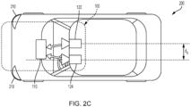
- Image capture devices 122, 124, and 126 can each include any type of device suitable for capturing at least one image from an environment. Moreover, any number of image capture devices can be used to acquire images for input to the image processor. Some examples of the presently disclosed subject matter can include or can be implemented with only a single-image capture device, while other examples can include or can be implemented with two, three, or even four or more image capture devices. Image capture devices 122, 124, and 126 will be further described with reference to figures 2B-2E , below.
- the system 100 can include or can be operatively associated with other types of sensors, including for example: an acoustic sensor, a RF sensor (e.g., radar transceiver), a LIDAR sensor.
- sensors can be used independently of or in cooperation with the image acquisition device 120.
- the data from the radar system (not shown) can be used for validating the processed information that is received from processing images acquired by the image acquisition device 120, e.g., to filter certain false positives resulting from processing images acquired by the image acquisition device 120, or it can be combined with or otherwise compliment the image data from the image acquisition device 120, or some processed variation or derivative of the image data from the image acquisition device 120.
- System 100 can be incorporated into various different platforms.
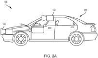
- system 100 may be included on a vehicle 200, as shown in figure 2A .
- vehicle 200 can be equipped with a processing unit 110 and any of the other components of system 100, as described above relative to figure 1 .
- vehicle 200 can be equipped with only a single-image capture device (e.g., camera), in other embodiments, such as those discussed in connection with figures 2B-2E , multiple image capture devices can be used.
- ADAS Advanced Driver Assistance Systems
- image capture devices included on vehicle 200 as part of the image acquisition unit 120 can be positioned at any suitable location.
- image capture device 122 can be located in the vicinity of the rearview mirror. This position may provide a line of sight similar to that of the driver of vehicle 200, which can aid in determining what is and is not visible to the driver.
- image capture device 124 can be located on or in a bumper of vehicle 200. Such a location can be especially suitable for image capture devices having a wide field of view. The line of sight of bumper-located image capture devices can be different from that of the driver.
- the image capture devices e.g., image capture devices 122, 124, and 126) can also be located in other locations.
- the image capture devices may be located on or in one or both of the side mirrors of vehicle 200, on the roof of vehicle 200, on the hood of vehicle 200, on the trunk of vehicle 200, on the sides of vehicle 200, mounted on, positioned behind, or positioned in front of any of the windows of vehicle 200, and mounted in or near light figures on the front and/or back of vehicle 200, etc.
- the image capture unit 120 or an image capture device that is one of a plurality of image capture devices that are used in an image capture unit 120, can have a field-of-view (FOV) that is different than the FOV of a driver of a vehicle, and not always see the same objects.
- FOV field-of-view
- disclosed embodiments are not limited to a particular type of vehicle 200 and may be applicable to all types of vehicles including automobiles, trucks, trailers, motorcycles, bicycles, self-balancing transport devices and other types of vehicles.
- the first image capture device 122 may have a scan rate associated with acquisition of each of the first series of image scan lines.
- the scan rate may refer to a rate at which an image sensor can acquire image data associated with each pixel included in a particular scan line.
- FIG. 2E is a diagrammatic representation of vehicle control systems, according to examples of the presently disclosed subject matter.
- vehicle 200 can include throttling system 220, braking system 230, and steering system 240.
- System 100 can provide inputs (e.g., control signals) to one or more of throttling system 220, braking system 230, and steering system 240 over one or more data links (e.g., any wired and/or wireless link or links for transmitting data).
- data links e.g., any wired and/or wireless link or links for transmitting data.
- system 100 can provide control signals to one or more of throttling system 220, braking system 230, and steering system 240 to navigate vehicle 200 (e.g., by causing an acceleration, a turn, a lane shift, etc.). Further, system 100 can receive inputs from one or more of throttling system 220, braking system 230, and steering system 240 indicating operating conditions of vehicle 200 (e.g., speed, whether vehicle 200 is braking and/or turning, etc.).
- vehicle 200 may also include a user interface 170 for interacting with a driver or a passenger of vehicle 200.
- user interface 170 in a vehicle application may include a touch screen 320, knobs 330, buttons 340, and a microphone 350.
- a driver or passenger of vehicle 200 may also use handles (e.g., located on or near the steering column of vehicle 200 including, for example, turn signal handles), buttons (e.g., located on the steering wheel of vehicle 200), and the like, to interact with system 100.
- handles e.g., located on or near the steering column of vehicle 200 including, for example, turn signal handles), buttons (e.g., located on the steering wheel of vehicle 200), and the like, to interact with system 100.
- microphone 350 may be positioned adjacent to a rearview mirror 310.
- image capture device 122 may be located near rearview mirror 310.
- user interface 170 may also include one or more speakers 360 (e.g., speakers of a vehicle audio system).
- system 100 may provide various notifications (e.g
- system 100 can provide a wide range of functionality to analyze the surroundings of vehicle 200 and, in response to this analysis, navigate and/or otherwise control and/or operate vehicle 200.
- Navigation, control, and/or operation of vehicle 200 may include enabling and/or disabling (directly or via intermediary controllers, such as the controllers mentioned above) various features, components, devices, modes, systems, and/or subsystems associated with vehicle 200.
- Navigation, control, and/or operation may alternately or additionally include interaction with a user, driver, passenger, passerby, and/or other vehicle or user, which may be located inside or outside vehicle 200, for example by providing visual, audio, haptic, and/or other sensory alerts and/or indications.
- system 100 may provide a variety of features related to autonomous driving, semi-autonomous driving and/or driver assist technology.
- system 100 may analyze image data, position data (e.g., GPS location information), map data, speed data, and/or data from sensors included in vehicle 200.
- System 100 may collect the data for analysis from, for example, image acquisition unit 120, position sensor 130, and other sensors. Further, system 100 may analyze the collected data to determine whether or not vehicle 200 should take a certain action, and then automatically take the determined action without human intervention. It would be appreciated that in some cases, the actions taken automatically by the vehicle are under human supervision, and the ability of the human to intervene adjust abort or override the machine action is enabled under certain circumstances or at all times.
- ECC error correction coding
- ECC on sensor images and especially lower resolution images such as radar sensor acquired images and LIDAR sensor acquired images increases the reliability of such images, reduces required level of redundancy and so allows using fewer number of sensors - thereby reducing the cost of the system, simplifying the system and reducing the size, and energy consumption of the system. Accordingly - applying the ECC on LIDAR images may replace the need of using redundant LIDAR sensors to compensate for LIDAR image errors.
- the low penalty associated with applying the ECC may ease the applying of ECC on the images acquired by the image acquisition unit 120 and also on any processed image (or temporary data) generated during any one out of autonomous driving operations, semi-autonomous driving operations and/or driver assist technology operations such as but not limited to automatic lane tracking, pedestrian detection, autonomous breaking, and the like.
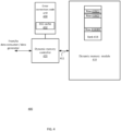
- FIG. 4 and 5 illustrates an example of a dynamic memory module 410 and a dynamic memory controller 420.
- the dynamic memory module may be a DRAM and/or a DDR (double data rate) memory module. In some of the examples below it is assumed that the dynamic memory module is a DDR memory module.
- An in-line ECC configuration may be used - in which the error correction sub-blocks (also referred to as ECC sub-blocks) and data sub-blocks are sent (from the dynamic memory module and to the dynamic memory module) over the same communication link - in a serial manner.
- ECC sub-blocks also referred to as ECC sub-blocks
- data sub-blocks are sent (from the dynamic memory module and to the dynamic memory module) over the same communication link - in a serial manner.
- ECC bits and data bits are sent over the same pins (or other interface) of the dynamic memory module - in a serial manner.
- the in-line ECC configuration may require only a single dynamic memory module for storing the ECC and data and is LPDDR4 compliant.
- the dynamic memory module may be, for example, any one of memory modules 140 and 150 of figure 1 .
- the dynamic memory module 410 may receive (over communication link 411) data sub-blocks that originated from data generators such as application processor 180 and image processor 190 of figure 1 (or from any other data generator).
- the dynamic memory module 410 may output (over communication link 411) data sub-blocks to data consumers such as application processor 180 and image processor 190 of figure 1 (or to any other data consumer).
- the dynamic memory controller is coupled to an ECC unit 430.
- the ECC unit 430 is included in the dynamic memory controller 420.
- the dynamic memory module 410 may include one or more memory banks.
- Figure 4 illustrates a single memory bank 418 while figure 5 illustrates eight memory banks 411-418.
- the dynamic memory module 410 may include any number of memory banks. For DDR use performance reasons, it's beneficial to store the ECC blocks together with the corresponding data blocks in the same DDR row.
- the ECC unit 430 may apply ECC operations on incoming data sub-blocks to provide ECC sub-blocks.
- a further trigger may be a need to buffer other data commands and LRU ECC may need to be replaced.
- the ECC unit 430 may apply ECC check on data sub-blocks read from the dynamic memory module 410 in order to detect errors and correct errors. Every data read from DDR requires a subsequent corresponding ECC read, unless this particular ECC is already present in ECC cache/buffer
- the ECC unit 430 may perform ECC operations (generation or check) on all the data stored in the dynamic memory module 410 or on predefined regions of the dynamic memory module 410 that require ECC protection.
- Figure 5 illustrates a row 418(2) of memory bank 418 of dynamic memory module 410 that stores seven data blocks 401-407 and an ECC block 408.
- Memory bank 418 may have any number of rows - and rows 418(1), 418(2) and 418(80) are only examples of some of the rows of memory bank 418.
- Each data block may include multiple data sub-blocks - for example data sub-blocks 410(1)-401(8) of data block 401.
- the data sub-blocks may be transferred during one or more data bursts.
- ECC block 408 may include ECC sub-blocks - for example ECC sub-blocks 408(1,1)-408(1,8) that are related to data sub-blocks 401(1)-401(8).
- the data blocks and the ECC block may be 512-byte long and each sub-block may be 64-byte long. Other sizes may be supported. The relationship between the size and/or number of the ECC block and the size and/or number of data blocks per row may differ from those illustrated in figure 5 .
- An ECC sub-block may be calculated by the ECC unit 430 whenever a data sub-block is received or in a later point of time.
- Dynamic memory module 410 may include one or more memory banks. In each memory bank, up to a single row may be opened (activated) at a time.
- a write operation to a certain row (that is currently closed) of the dynamic memory module 410 requires to close another row (that is currently open), activate the certain row and write one or more data sub-blocks to the certain row.
- tRP Row precharge time
- tRCD RAS-to-CAS delay
- WL write latency
- the dynamic memory controller 420 controls the various operations related to the dynamic memory module 410 (including the write operation, the pre-charging operation and the activating operation) and may determine when to perform the writing of the one or more ECC sub-blocks before the certain row is closed.
- the dynamic memory controller 420 may receive access requests (denoted 442 in figure 5 ) and convert these access requests to dynamic memory controller commands such as pre-charging row, activate row and read or write row (see box 443 in figure 5 ).
- FIG. 5 illustrates two triplets of dynamic memory controller commands:
- the dynamic memory controller commands may include:
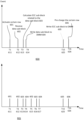
- Figure 6 illustrates two timing diagrams 600 and 602.
- Timing diagram 600 illustrates the following sequence of events (T denotes a point in time):
- event 603 may follow event 604, that events 603 and 604 may occur simultaneously.
- the writing of the data sub-blocks to the dynamic memory module may be executed upon a reception of a single data sub-block, that multiple data sub-blocks may be aggregated before they are written to the dynamic memory module, and the like.
- Timing diagram 602 illustrates two repetitions of events 602, 603 and 604 before the occurrence of event 605.
- Timing diagram 600 illustrates the following sequence of events (T denotes a point in time):
- Figure 7 is a flow chart that illustrates method 700.
- Method 700 may start by step 702 of activating a certain row of a dynamic memory module.
- Step 702 may be triggered by a write command that is received by a dynamic memory controller.
- Step 702 may be followed by step 704 of receiving (by a dynamic memory controller) a data sub-block to be written to the certain row of the dynamic memory module.
- a data sub-block to be written to (or targeted to) the certain row may be associated (by the dynamic memory controller or by another entity) with address information that indicates that the data-sub-block should be written to the certain row.
- Step 704 may be followed by steps 706 and 708.
- Step 706 may include calculating an ECC sub-block related to (protecting) the data sub-block.
- Step 708 may include writing the data sub-block to the dynamic memory module over the communication link.
- Steps 706 and 708 may be followed by step 720 of writing one or more ECC sub-blocks to the certain row before the certain row is pre-charged.
- the writing of the data unit to the dynamic memory module includes sending the data unit over the communication link.
- Method 700 utilizes the in-line ECC configuration - the same communication line is used for conveying data bits and ECC bits - at different points of time.
- Steps 702-720 may be repeated for multiple rows - especially one row after the other. Each iteration a row is selected and after steps 702-720 are executed the method may be executed in relation to a new selected row.
- the certain row of figure 7 is an example of a selected row.
- Method 700 may, for example, be executed as a part of a ADAS operation and/or an autonomous vehicle operation. Method 700 may be used for any other purpose.
- Figure 8 illustrates a method 700 that further includes step 707 of storing the ECC sub-block related to the data sub-block in a cache memory (for example ECC cache 432 of figure 5 ).
- Step 707 follows step 706 and precedes step 708.
- steps 704, 706 and 708 may occur between the execution of steps 702 and 720.
- the computer program product is non-transitory and may be, for example, an integrated circuit, a magnetic memory, an optical memory, a disk, and the like.
- Any reference to a computer program product should be applied, mutatis mutandis to a method that is executed by a system and/or a system that is configured to execute the instructions stored in the computer program product.
- any arrangement of components to achieve the same functionality is effectively “associated” such that the desired functionality is achieved.
- any two components herein combined to achieve a particular functionality may be seen as “associated with” each other such that the desired functionality is achieved, irrespective of architectures or intermedial components.
- any two components so associated can also be viewed as being “operably connected,” or “operably coupled,” to each other to achieve the desired functionality.
- condition X may be fulfilled. This phrase also suggests that condition X may not be fulfilled. For example - any reference to a system as including a certain component should also cover the scenario in which the system does not include the certain component.
- any method may include at least the steps included in the figures and/or in the specification, only the steps included in the figures and/or the specification. The same applies to the system and the mobile computer.
- the illustrated examples may be implemented as circuitry located on a single integrated circuit or within a same device.
- the examples may be implemented as any number of separate integrated circuits or separate devices interconnected with each other in a suitable manner.
- the examples, or portions thereof may implemented as soft or code representations of physical circuitry or of logical representations convertible into physical circuitry, such as in a hardware description language of any appropriate type.
- the invention is not limited to physical devices or units implemented in non-programmable hardware but can also be applied in programmable devices or units able to perform the desired device functions by operating in accordance with suitable program code, such as mainframes, minicomputers, servers, workstations, personal computers, notepads, personal digital assistants, electronic games, automotive and other embedded systems, cell phones and various other wireless devices, commonly denoted in this application as 'computer systems'.
- suitable program code such as mainframes, minicomputers, servers, workstations, personal computers, notepads, personal digital assistants, electronic games, automotive and other embedded systems, cell phones and various other wireless devices, commonly denoted in this application as 'computer systems'.
- any reference signs placed between parentheses shall not be construed as limiting the claim.
- the word 'comprising' does not exclude the presence of other elements or steps then those listed in a claim.
- the terms "a” or “an,” as used herein, are defined as one as or more than one.
- the use of introductory phrases such as “at least one " and “one or more " in the claims should not be construed to imply that the introduction of another claim element by the indefinite articles "a " or “an " limits any particular claim containing such introduced claim element to inventions containing only one such element, even when the same claim includes the introductory phrases “one or more " or “at least one " and indefinite articles such as "a " or “an.
Landscapes
- Engineering & Computer Science (AREA)
- Theoretical Computer Science (AREA)
- Physics & Mathematics (AREA)
- Quality & Reliability (AREA)
- General Engineering & Computer Science (AREA)
- General Physics & Mathematics (AREA)
- Computing Systems (AREA)
- Mathematical Physics (AREA)
- Traffic Control Systems (AREA)
Claims (15)
- Verfahren zur Fehlerkorrektur, wobei das Verfahren die folgenden Schritte umfasst:Öffnen einer ausgewählten Zeile (418(2)) einer Speicherbank (418) aus mehreren Speicherbänken (411, 418) eines dynamischen Speichermoduls (410);Empfangen ausgewählter Daten-Teilblöcke (401(1), ..., (401(8)), während die ausgewählte Zeile (418(2)) geöffnet ist, durch das dynamische Speichermodul (410), wobei die ausgewählten Daten-Teilblöcke (401(1), ..., (401(8)) über eine Kommunikationsverbindung empfangen werden und darauf ausgelegt sind, in die ausgewählte Zeile (418(2)) geschrieben zu werden;Berechnen, während die ausgewählte Zeile (418(2)) geöffnet ist und durch eine Fehlerkorrektureinheit (430), von ausgewählten Fehlerkorrekturcode-Teilblöcken (408(1,1), ..., 401(1,8)), die sich auf die ausgewählten Daten-Teilblöcke (401(1), ..., (401(8)) beziehen;Zwischenspeichern der ausgewählten Fehlerkorrekturcode-Teilblöcke (408(1,1), ..., 401(1,8)) in einem Zwischenspeicher (432), der sich von dem dynamischen Speichermodul (410) unterscheidet;Schließen der ausgewählten Zeile (418(2)); undSchreiben, durch eine dynamische Speichersteuerung und in die ausgewählte Zeile (418(2)), der ausgewählten Fehlerkorrekturcode-Teilblöcke (408(1,1), ..., 401(1,8)) in die ausgewählte Zeile (418(2)), während die ausgewählte Zeile (418(2)) geöffnet ist, wobei das Schreiben das Senden der ausgewählten Fehlerkorrekturcode-Teilblöcke (408(1,1), ..., 401(1,8)) an das dynamische Speichermodul (410) über die Kommunikationsverbindung umfasst;dadurch gekennzeichnet, dassdas Schreiben der ausgewählten Fehlerkorrekturcode-Teilblöcke in das dynamische Speichermodul (410) durch eine Notwendigkeit ausgelöst wird, einen Zustand der dynamischen Speichersteuerung (420) vor dem Eintreten in Modi mit geringer Leistungsaufnahme zu bereinigen.
- Verfahren nach Anspruch 1, wobei das Schließen der ausgewählten Zeile
(418(2)) das Vorladen der ausgewählten Zeile (418(2)) umfasst. - Verfahren nach Anspruch 1 oder 2, ferner umfassend den Schritt des
Speicherns, in der ausgewählten Zeile (418(2)), mehrerer Daten-Teilblöcke (401(1), ..., (401(8)) als Fehlerkorrekturcode-Teilblöcke (408(1,1), ..., 401(1,8)). - Verfahren nach einem der Ansprüche 1 bis 3, umfassend das Speichern, in der
ausgewählten Zeile (418(2)), von Datenblöcken (401, 402, ..., 407) und eines einzelnen Fehlerkorrekturcode-Blocks (408), wobei jeder Datenblock (401, 402, ..., 407) Daten-Teilblöcke (401(1), ..., (401(8)) umfasst, und wobei der einzelne Fehlerkorrekturcode-Block (408) die Fehlerkorrekturcode-Teilblöcke (408(1,1), ..., 401(1,8)) umfasst. - Verfahren nach einem der Ansprüche 1 bis 4, umfassend:Öffnen einer neuen ausgewählten Zeile, die zu einer beliebigen der mehreren Speicherbänke (411, 418) gehört;Empfangen, durch das dynamische Speichermodul (410), über die Kommunikationsverbindung, und während die neue ausgewählte Zeile geöffnet ist, neuer ausgewählter Daten-Teilblöcke (401(1), ..., (401(8)), die darauf ausgelegt sind, in die neue ausgewählte Zeile geschrieben zu werden;Berechnen, durch die Fehlerkorrektureinheit (430), während die neue ausgewählte Zeile geöffnet ist, neuer ausgewählter Fehlerkorrekturcode-Teilblöcke (408(1,1), ..., 401(1,8)), die sich auf die neuen ausgewählten Daten-Teilblöcke (401(1), ..., (401(8)) beziehen;Zwischenspeichern der neuen ausgewählten Fehlerkorrekturcode-Teilblöcke (408(1,1), ..., 401(1,8)) in dem Zwischenspeicher (432);Schreiben, in die neue ausgewählte Zeile, der neuen ausgewählten Fehlerkorrekturcode-Teilblöcke (408(1,1), ..., 401(1,8)), während die neue ausgewählte Zeile geöffnet ist; wobei das Schreiben das Senden der neuen ausgewählten Fehlerkorrekturcode-Teilblöcke (408(1,1), ..., 401(1,8)) an das dynamische Speichermodul (410) über die Kommunikationsverbindung umfasst; undSchließen der neuen ausgewählten Zeile.
- Verfahren nach einem der Ansprüche 1 bis 5, umfassend:Empfangen einer Anforderung zum Lesen einer ersten Vielzahl von Daten-Teilblöcken (401(1), ..., (401(8)), die in unterschiedlichen Speicherbänken (411, 418) der mehreren Speicherbänke (411, 418) des dynamischen Speichermoduls (410) gespeichert sind;Prüfen, ob der Zwischenspeicher (432) Fehlerkorrekturcode-Teilblöcke (408(1,1), ..., 401(1,8)) speichert, die sich auf einen beliebigen der ersten Vielzahl von Daten-Teilblöcken (401(1), ..., (401(8)) beziehen;Abrufen, aus dem dynamischen Speichermodul (410) und über die Kommunikationsverbindung, der ersten Vielzahl von Daten-Teilblöcken (401(1), ..., (401(8));Abrufen von Fehlerkorrekturcode-Teilblöcken (408(1,1), ..., 401(1,8)), die sich auf die erste Vielzahl von Daten-Teilblöcken (401(1), ..., (401(8)) beziehen; wobei das Abrufen das Abrufen, aus dem Zwischenspeicher (432) statt aus dem dynamischen Speichermodul (410), eines beliebigen Fehlerkorrekturcode-Teilblocks (408(1,1), ..., 401(1,8)), der in dem Zwischenspeicher (432) gespeichert ist und sich auf einen beliebigen der ersten Vielzahl von Daten-Teilblöcken (401(1), ..., (401(8)) bezieht, umfasst; undFehlerkorrektur der ersten Vielzahl von Daten-Teilblöcken (401(1), ..., (401(8)), um eine erste Vielzahl von fehlerkorrigierten Daten-Teilblöcken (401(1), ..., (401(8)) unter Verwendung der Fehlerkorrekturcode-Teilblöcke (408(1,1), ..., 401(1,8)), die sich auf die erste Vielzahl von Daten-Teilblöcken (401(1), ..., (401(8)) beziehen, bereitzustellen.
- System mit Fehlerkorrekturfähigkeiten, wobei das System eine dynamische Speichersteuerung (420), ein dynamisches Speichermodul (410), das mit einer Kommunikationsverbindung gekoppelt ist, einen Zwischenspeicher (432) und eine Fehlerkorrekturcodeeinheit (430) umfasst;wobei die dynamische Speichersteuerung (420) konfiguriert ist, um eine ausgewählte Zeile (418(2)) einer Speicherbank (418) aus mehreren Speicherbänken (411, 418) eines dynamischen Speichermoduls (410) zu öffnen und, während die ausgewählte Zeile (418(2)) geöffnet ist, ausgewählte Daten-Teilblöcke (401(1), ..., (401(8)) zu empfangen, die darauf ausgelegt sind, in die ausgewählte Zeile (418(2)) geschrieben zu werden;wobei das dynamische Speichermodul (410) konfiguriert ist, um die ausgewählten Daten-Teilblöcke (401(1), ..., (401(8)) von der dynamischen Speichersteuerung (420) und über eine Kommunikationsverbindung zu empfangen;wobei die Fehlerkorrektureinheit (430) konfiguriert ist, um, während die ausgewählte Zeile (418(2)) geöffnet ist, ausgewählte Fehlerkorrekturcode-Teilblöcke (408(1,1), ..., 401(1,8)) zu berechnen, die sich auf die ausgewählten Daten-Teilblöcke (401(1), ..., (401(8)) beziehen;wobei sich der Zwischenspeicher (432) von dem dynamischen Speichermodul (410) unterscheidet und konfiguriert ist, die ausgewählten Fehlerkorrekturcode-Teilblöcke (408(1,1), ..., 401(1,8)) zwischenzuspeichern;wobei die dynamische Speichersteuerung (420) ferner konfiguriert ist zum:Senden der ausgewählten Fehlerkorrekturcode-Teilblöcke (408(1,1), ..., 401(1,8)) über die Kommunikationsverbindung an das dynamische Speichermodul (410),Schreiben, in die ausgewählte Zeile (418(2)) und über die Kommunikationsverbindung, der ausgewählten Fehlerkorrekturcode-Teilblöcke (408(1,1), ..., 401(1,8)), während die ausgewählte Zeile (418(2)) geöffnet ist, wobei das Schreiben der ausgewählten Fehlerkorrekturcode-Teilblöcke in das dynamische Speichermodul (410) durch eine Notwendigkeit ausgelöst wird, einen Zustand der dynamischen Speichersteuerung (420) vor dem Eintreten in Modi mit geringer Leistungsaufnahme zu bereinigen; undSchließen der ausgewählten Zeile (418(2)).
- System nach Anspruch 7, wobei die dynamische Speichersteuerung (420) die Fehlerkorrekturcodeeinheit (430) und den Zwischenspeicher (432) umfasst.
- System nach Anspruch 7, wobei die dynamische Speichersteuerung (420) mit der Fehlerkorrekturcodeeinheit (430) und dem Zwischenspeicher (432) gekoppelt ist.
- System nach einem der Ansprüche 7 bis 9, wobei die dynamische Speichersteuerung (420) konfiguriert ist, um die ausgewählte Zeile (418(2)) durch Vorladen der ausgewählten Zeile (418(2)) zu schließen.
- System nach einem der Ansprüche 7 bis 10, wobei das dynamische Speichermodul (410) konfiguriert ist, um in der ausgewählten Zeile (418(2)) mehr Daten-Teilblöcke (401(1), ..., (401(8)) als Fehlerkorrekturcode-Teilblöcke (408(1,1), ..., 401(1,8)) zu speichern.
- System nach einem der Ansprüche 7 bis 11, wobei das dynamische Speichermodul (410) konfiguriert ist, um in der ausgewählten Zeile (418(2)) Datenblöcke (401, 402, ..., 407) und einen einzelnen Fehlerkorrekturcodeblock (408) zu speichern, wobei jeder Datenblock (401, 402, ..., 407) Daten-Teilblöcke (401(1), ..., (401(8)) umfasst, und wobei der einzelne Fehlerkorrekturcode-Block (408) Fehlerkorrekturcode-Teilblöcke (408(1,1), ..., 401(1,8)) umfasst.
- System nach einem der Ansprüche 7 bis 12, wobei die dynamische Speichersteuerung (420) konfiguriert ist zum:Öffnen einer neuen ausgewählten Zeile einer beliebigen Speicherbank (418) der mehreren Speicher, undEmpfangen, während die neue ausgewählte Zeile geöffnet ist, neuer ausgewählter Daten-Teilblöcke (401(1), ..., (401(8)), die darauf ausgelegt sind, in die ausgewählte Zeile (418(2)) geschrieben zu werden; (c) Senden der neuen ausgewählten Daten-Teilblöcke (401(1), ..., (401(8)) an das dynamische Speichermodul (410) über die Kommunikationsverbindung;wobei die Fehlerkorrektureinheit (430) konfiguriert ist, um, während die neue ausgewählte Zeile geöffnet ist, neue ausgewählte Fehlerkorrekturcode-Teilblöcke (408(1,1), ..., 401(1,8)) zu berechnen, die sich auf die neuen ausgewählten Daten-Teilblöcke (401(1), ..., (401(8)) beziehen; undwobei die dynamische Speichersteuerung (420) ferner konfiguriert ist zum:Schreiben, in die neue ausgewählte Zeile über die Kommunikationsverbindung, der neuen ausgewählten Fehlerkorrekturcode-Teilblöcke (408(1,1), ..., 401(1,8)), während die neue ausgewählte Zeile geöffnet ist, undSchließen der neuen ausgewählten Zeile.
- System nach einem der Ansprüche 7 bis 13, wobei die dynamische Speichersteuerung (420) konfiguriert ist zum:Empfangen einer Anforderung zum Lesen einer ersten Vielzahl von Daten-Teilblöcken (401(1), ..., (401(8)), die in unterschiedlichen Speicherbänken (418) der mehreren Speicherbänke (411, 418) des dynamischen Speichermoduls (410) gespeichert sind,Prüfen, ob der Zwischenspeicher (432) Fehlerkorrekturcode-Teilblöcke (408(1,1), ..., 401(1,8)) speichert, die sich auf einen beliebigen der ersten Vielzahl von Daten-Teilblöcken (401(1), ..., (401(8)) beziehen;Abrufen, aus dem dynamischen Speichermodul (410), der ersten Vielzahl von Daten-Teilblöcken (401(1), ..., (401(8)), undAbrufen von Fehlerkorrekturcode-Teilblöcken (408(1,1), ..., 401(1,8)), die sich auf die erste Vielzahl von Daten-Teilblöcken (401(1), ..., (401(8)) beziehen;wobei das Abrufen der Fehlerkorrekturcode-Teilblöcke (408(1,1), ..., 401(1,8)) das Abrufen, aus dem Zwischenspeicher (432) statt aus dem dynamischen Speichermodul (410), eines beliebigen Fehlerkorrekturcode-Teilblocks (408(1,1), ..., 401(1,8)), der in dem Zwischenspeicher (432) gespeichert ist und sich auf einen beliebigen der ersten Vielzahl von Daten-Teilblöcken (401(1), ..., (401(8)) bezieht, umfasst; undwobei die Fehlerkorrektureinheit (430) konfiguriert ist, eine Fehlerkorrektur der ersten Vielzahl von Daten-Teilblöcken (401(1), ..., (401(8)) durchzuführen, um eine erste Vielzahl von fehlerkorrigierten Daten-Teilblöcken (401(1), ..., (401(8)) unter Verwendung der Fehlerkorrekturcode-Teilblöcke (408(1,1), ..., 401(1,8)), die sich auf die erste Vielzahl von Daten-Teilblöcken (401(1), ..., (401(8)) beziehen, bereitzustellen.
- Computerprogrammprodukt, das Anweisungen speichert, die, sobald sie durch ein computergestütztes System ausgeführt werden, das computergestützte System veranlassen, die folgenden Schritte auszuführen:Öffnen einer ausgewählten Zeile (418(2)) einer Speicherbank (418) aus mehreren Speicherbänken (411, 418) eines dynamischen Speichermoduls (410);Empfangen ausgewählter Daten-Teilblöcke (401(1), ..., (401(8)), während die ausgewählte Zeile (418(2)) geöffnet ist, durch das dynamische Speichermodul (410), wobei die ausgewählten Daten-Teilblöcke (401(1), ..., (401(8)) über eineKommunikationsverbindung empfangen werden und darauf ausgelegt sind, in die ausgewählte Zeile (418(2)) geschrieben zu werden;Berechnen, während die ausgewählte Zeile (418(2)) geöffnet ist und durch eine Fehlerkorrektureinheit (430), von ausgewählten Fehlerkorrekturcode-Teilblöcken (408(1,1), ..., 401(1,8)), die sich auf die ausgewählten Daten-Teilblöcke (401(1), ..., (401(8)) beziehen;Zwischenspeichern der ausgewählten Fehlerkorrekturcode-Teilblöcke (408(1,1), ..., 401(1,8)) in einem Zwischenspeicher (432), der sich von dem dynamischen Speichermodul (410) unterscheidet;Schreiben, in die ausgewählte Zeile (418(2)), der ausgewählten Fehlerkorrekturcode-Teilblöcke (408(1,1), ..., 401(1,8)), während die ausgewählte Zeile (418(2)) geöffnet ist; wobei das Schreiben das Senden der ausgewählten Fehlerkorrekturcode-Teilblöcke (408(1,1), ..., 401(1,8)) an das dynamische Speichermodul (410) über die Kommunikationsverbindung umfasst, wobei das Schreiben der ausgewählten Fehlerkorrekturcode-Teilblöcke an das dynamische Speichermodul (410) durch eine Notwendigkeit ausgelöst wird, einen Zustand der dynamischen Speichersteuerung (420) vor dem Eintreten in Modi mit geringer Leistungsaufnahme zu bereinigen; und Schließen der ausgewählten Zeile (418(2)).
Applications Claiming Priority (2)
| Application Number | Priority Date | Filing Date | Title |
|---|---|---|---|
| US201762486006P | 2017-04-17 | 2017-04-17 | |
| PCT/IL2018/050431 WO2018193448A1 (en) | 2017-04-17 | 2018-04-17 | Systems and methods for error correction |
Publications (2)
| Publication Number | Publication Date |
|---|---|
| EP3612939A1 EP3612939A1 (de) | 2020-02-26 |
| EP3612939B1 true EP3612939B1 (de) | 2025-04-16 |
Family
ID=62152603
Family Applications (1)
| Application Number | Title | Priority Date | Filing Date |
|---|---|---|---|
| EP18724340.7A Active EP3612939B1 (de) | 2017-04-17 | 2018-04-17 | System und verfahren zur fehlerkorrektur |
Country Status (4)
| Country | Link |
|---|---|
| US (1) | US11366717B2 (de) |
| EP (1) | EP3612939B1 (de) |
| CN (1) | CN110799947B (de) |
| WO (1) | WO2018193448A1 (de) |
Families Citing this family (4)
| Publication number | Priority date | Publication date | Assignee | Title |
|---|---|---|---|---|
| EP3612939B1 (de) | 2017-04-17 | 2025-04-16 | Mobileye Vision Technologies Ltd. | System und verfahren zur fehlerkorrektur |
| CA3030580C (en) * | 2017-04-27 | 2021-06-29 | Beijing Didi Infinity Technology And Development Co., Ltd. | Systems and methods for determining an estimated time of arrival |
| WO2020026029A2 (en) | 2018-08-03 | 2020-02-06 | Mobileye Vision Technologies Ltd. | Error correction coding in a dynamic memory module |
| CN112219197B (zh) * | 2019-03-08 | 2024-01-23 | 御眼视觉技术有限公司 | 基于优先级的共享资源访问管理 |
Family Cites Families (18)
| Publication number | Priority date | Publication date | Assignee | Title |
|---|---|---|---|---|
| USRE47908E1 (en) * | 1991-12-23 | 2020-03-17 | Blanding Hovenweep, Llc | Ergonomic man-machine interface incorporating adaptive pattern recognition based control system |
| US20020116679A1 (en) * | 2000-12-15 | 2002-08-22 | Mike Lei | In-band FEC decoder for sonet |
| US7117421B1 (en) * | 2002-05-31 | 2006-10-03 | Nvidia Corporation | Transparent error correction code memory system and method |
| US7836380B2 (en) * | 2006-10-31 | 2010-11-16 | Intel Corporation | Destination indication to aid in posted write buffer loading |
| US9152496B2 (en) * | 2007-12-21 | 2015-10-06 | Cypress Semiconductor Corporation | High performance flash channel interface |
| KR101036833B1 (ko) * | 2010-03-31 | 2011-05-25 | 국방과학연구소 | 표적 추적 시스템의 레이다 센서와 영상 센서 간의 정렬오차 추정 장치 및 방법 |
| US8644104B2 (en) * | 2011-01-14 | 2014-02-04 | Rambus Inc. | Memory system components that support error detection and correction |
| EP3188188B1 (de) | 2011-01-31 | 2021-09-01 | Everspin Technologies, Inc. | Selbstreferenzleseverfahren eines magnetischen direktzugriffsspeichers mit einem drall-drehmoment |
| US10474584B2 (en) * | 2012-04-30 | 2019-11-12 | Hewlett Packard Enterprise Development Lp | Storing cache metadata separately from integrated circuit containing cache controller |
| US20140089755A1 (en) * | 2012-09-27 | 2014-03-27 | Shveta KANTAMSETTI | Reliability enhancements for high speed memory - parity protection on command/address and ecc protection on data |
| US8947918B2 (en) * | 2013-03-22 | 2015-02-03 | Katsuyuki Fujita | Semiconductor memory device |
| US10146601B2 (en) * | 2013-06-12 | 2018-12-04 | Everspin Technologies, Inc. | Methods and devices for healing reset errors in a magnetic memory |
| WO2015009331A1 (en) * | 2013-07-15 | 2015-01-22 | Everspin Technologies, Inc. | Memory device with page emulation mode |
| US9472261B1 (en) * | 2015-04-17 | 2016-10-18 | Qualcomm Incorporated | Systems and methods to refresh DRAM based on temperature and based on calibration data |
| US10599150B2 (en) * | 2016-09-29 | 2020-03-24 | The Charles Stark Kraper Laboratory, Inc. | Autonomous vehicle: object-level fusion |
| US10198655B2 (en) * | 2017-01-24 | 2019-02-05 | Ford Global Technologies, Llc | Object detection using recurrent neural network and concatenated feature map |
| EP3612939B1 (de) | 2017-04-17 | 2025-04-16 | Mobileye Vision Technologies Ltd. | System und verfahren zur fehlerkorrektur |
| KR102088207B1 (ko) * | 2018-06-01 | 2020-03-12 | 주식회사 티맥스 소프트 | 서버, 서버를 제어하는 방법 및 컴퓨터 판독 가능 매체에 저장된 컴퓨터 프로그램 |
-
2018
- 2018-04-17 EP EP18724340.7A patent/EP3612939B1/de active Active
- 2018-04-17 WO PCT/IL2018/050431 patent/WO2018193448A1/en not_active Ceased
- 2018-04-17 CN CN201880025612.2A patent/CN110799947B/zh active Active
- 2018-04-17 US US16/605,620 patent/US11366717B2/en active Active
Also Published As
| Publication number | Publication date |
|---|---|
| US20210279131A1 (en) | 2021-09-09 |
| WO2018193448A1 (en) | 2018-10-25 |
| EP3612939A1 (de) | 2020-02-26 |
| US11366717B2 (en) | 2022-06-21 |
| CN110799947B (zh) | 2024-12-24 |
| CN110799947A (zh) | 2020-02-14 |
Similar Documents
| Publication | Publication Date | Title |
|---|---|---|
| US11951998B2 (en) | Secure system that includes driving related systems | |
| EP3612939B1 (de) | System und verfahren zur fehlerkorrektur | |
| US12086239B2 (en) | Secure distributed execution of jobs | |
| US20220253221A1 (en) | Accessing a dynamic memory module | |
| US10998023B2 (en) | Error correction coding in a dynamic memory module | |
| US12067388B2 (en) | Updating software elements with different trust levels | |
| US12554581B2 (en) | Multi-part compare and exchange operation | |
| US20220366215A1 (en) | Applying a convolution kernel on input data | |
| US20200353884A1 (en) | System on chip | |
| US12288085B2 (en) | On the fly configuration of a processing circuit |
Legal Events
| Date | Code | Title | Description |
|---|---|---|---|
| STAA | Information on the status of an ep patent application or granted ep patent |
Free format text: STATUS: UNKNOWN |
|
| STAA | Information on the status of an ep patent application or granted ep patent |
Free format text: STATUS: THE INTERNATIONAL PUBLICATION HAS BEEN MADE |
|
| PUAI | Public reference made under article 153(3) epc to a published international application that has entered the european phase |
Free format text: ORIGINAL CODE: 0009012 |
|
| STAA | Information on the status of an ep patent application or granted ep patent |
Free format text: STATUS: REQUEST FOR EXAMINATION WAS MADE |
|
| 17P | Request for examination filed |
Effective date: 20191017 |
|
| AK | Designated contracting states |
Kind code of ref document: A1 Designated state(s): AL AT BE BG CH CY CZ DE DK EE ES FI FR GB GR HR HU IE IS IT LI LT LU LV MC MK MT NL NO PL PT RO RS SE SI SK SM TR |
|
| AX | Request for extension of the european patent |
Extension state: BA ME |
|
| DAV | Request for validation of the european patent (deleted) | ||
| DAX | Request for extension of the european patent (deleted) | ||
| STAA | Information on the status of an ep patent application or granted ep patent |
Free format text: STATUS: EXAMINATION IS IN PROGRESS |
|
| 17Q | First examination report despatched |
Effective date: 20210224 |
|
| GRAP | Despatch of communication of intention to grant a patent |
Free format text: ORIGINAL CODE: EPIDOSNIGR1 |
|
| STAA | Information on the status of an ep patent application or granted ep patent |
Free format text: STATUS: GRANT OF PATENT IS INTENDED |
|
| INTG | Intention to grant announced |
Effective date: 20241112 |
|
| GRAS | Grant fee paid |
Free format text: ORIGINAL CODE: EPIDOSNIGR3 |
|
| GRAA | (expected) grant |
Free format text: ORIGINAL CODE: 0009210 |
|
| STAA | Information on the status of an ep patent application or granted ep patent |
Free format text: STATUS: THE PATENT HAS BEEN GRANTED |
|
| AK | Designated contracting states |
Kind code of ref document: B1 Designated state(s): AL AT BE BG CH CY CZ DE DK EE ES FI FR GB GR HR HU IE IS IT LI LT LU LV MC MK MT NL NO PL PT RO RS SE SI SK SM TR |
|
| REG | Reference to a national code |
Ref country code: GB Ref legal event code: FG4D |
|
| REG | Reference to a national code |
Ref country code: CH Ref legal event code: EP Ref country code: DE Ref legal event code: R096 Ref document number: 602018081120 Country of ref document: DE |
|
| REG | Reference to a national code |
Ref country code: IE Ref legal event code: FG4D |
|
| REG | Reference to a national code |
Ref country code: NL Ref legal event code: FP |
|
| RAP4 | Party data changed (patent owner data changed or rights of a patent transferred) |
Owner name: MOBILEYE VISION TECHNOLOGIES LTD. |
|
| REG | Reference to a national code |
Ref country code: AT Ref legal event code: MK05 Ref document number: 1786217 Country of ref document: AT Kind code of ref document: T Effective date: 20250416 |
|
| PG25 | Lapsed in a contracting state [announced via postgrant information from national office to epo] |
Ref country code: PT Free format text: LAPSE BECAUSE OF FAILURE TO SUBMIT A TRANSLATION OF THE DESCRIPTION OR TO PAY THE FEE WITHIN THE PRESCRIBED TIME-LIMIT Effective date: 20250818 Ref country code: FI Free format text: LAPSE BECAUSE OF FAILURE TO SUBMIT A TRANSLATION OF THE DESCRIPTION OR TO PAY THE FEE WITHIN THE PRESCRIBED TIME-LIMIT Effective date: 20250416 Ref country code: ES Free format text: LAPSE BECAUSE OF FAILURE TO SUBMIT A TRANSLATION OF THE DESCRIPTION OR TO PAY THE FEE WITHIN THE PRESCRIBED TIME-LIMIT Effective date: 20250416 |
|
| PGFP | Annual fee paid to national office [announced via postgrant information from national office to epo] |
Ref country code: DE Payment date: 20250630 Year of fee payment: 8 |
|
| REG | Reference to a national code |
Ref country code: LT Ref legal event code: MG9D |
|
| PG25 | Lapsed in a contracting state [announced via postgrant information from national office to epo] |
Ref country code: NO Free format text: LAPSE BECAUSE OF FAILURE TO SUBMIT A TRANSLATION OF THE DESCRIPTION OR TO PAY THE FEE WITHIN THE PRESCRIBED TIME-LIMIT Effective date: 20250716 Ref country code: GR Free format text: LAPSE BECAUSE OF FAILURE TO SUBMIT A TRANSLATION OF THE DESCRIPTION OR TO PAY THE FEE WITHIN THE PRESCRIBED TIME-LIMIT Effective date: 20250717 |
|
| PG25 | Lapsed in a contracting state [announced via postgrant information from national office to epo] |
Ref country code: PL Free format text: LAPSE BECAUSE OF FAILURE TO SUBMIT A TRANSLATION OF THE DESCRIPTION OR TO PAY THE FEE WITHIN THE PRESCRIBED TIME-LIMIT Effective date: 20250416 |
|
| PG25 | Lapsed in a contracting state [announced via postgrant information from national office to epo] |
Ref country code: BG Free format text: LAPSE BECAUSE OF FAILURE TO SUBMIT A TRANSLATION OF THE DESCRIPTION OR TO PAY THE FEE WITHIN THE PRESCRIBED TIME-LIMIT Effective date: 20250416 |
|
| PG25 | Lapsed in a contracting state [announced via postgrant information from national office to epo] |
Ref country code: HR Free format text: LAPSE BECAUSE OF FAILURE TO SUBMIT A TRANSLATION OF THE DESCRIPTION OR TO PAY THE FEE WITHIN THE PRESCRIBED TIME-LIMIT Effective date: 20250416 |
|
| PG25 | Lapsed in a contracting state [announced via postgrant information from national office to epo] |
Ref country code: AT Free format text: LAPSE BECAUSE OF FAILURE TO SUBMIT A TRANSLATION OF THE DESCRIPTION OR TO PAY THE FEE WITHIN THE PRESCRIBED TIME-LIMIT Effective date: 20250416 |
|
| PG25 | Lapsed in a contracting state [announced via postgrant information from national office to epo] |
Ref country code: RS Free format text: LAPSE BECAUSE OF FAILURE TO SUBMIT A TRANSLATION OF THE DESCRIPTION OR TO PAY THE FEE WITHIN THE PRESCRIBED TIME-LIMIT Effective date: 20250716 |
|
| PG25 | Lapsed in a contracting state [announced via postgrant information from national office to epo] |
Ref country code: IS Free format text: LAPSE BECAUSE OF FAILURE TO SUBMIT A TRANSLATION OF THE DESCRIPTION OR TO PAY THE FEE WITHIN THE PRESCRIBED TIME-LIMIT Effective date: 20250816 |
|
| PG25 | Lapsed in a contracting state [announced via postgrant information from national office to epo] |
Ref country code: LV Free format text: LAPSE BECAUSE OF FAILURE TO SUBMIT A TRANSLATION OF THE DESCRIPTION OR TO PAY THE FEE WITHIN THE PRESCRIBED TIME-LIMIT Effective date: 20250416 |
|
| REG | Reference to a national code |
Ref country code: CH Ref legal event code: H13 Free format text: ST27 STATUS EVENT CODE: U-0-0-H10-H13 (AS PROVIDED BY THE NATIONAL OFFICE) Effective date: 20251125 |
|
| PG25 | Lapsed in a contracting state [announced via postgrant information from national office to epo] |
Ref country code: LU Free format text: LAPSE BECAUSE OF NON-PAYMENT OF DUE FEES Effective date: 20250417 |
|
| REG | Reference to a national code |
Ref country code: BE Ref legal event code: MM Effective date: 20250430 |
|
| PG25 | Lapsed in a contracting state [announced via postgrant information from national office to epo] |
Ref country code: DK Free format text: LAPSE BECAUSE OF FAILURE TO SUBMIT A TRANSLATION OF THE DESCRIPTION OR TO PAY THE FEE WITHIN THE PRESCRIBED TIME-LIMIT Effective date: 20250416 Ref country code: SM Free format text: LAPSE BECAUSE OF FAILURE TO SUBMIT A TRANSLATION OF THE DESCRIPTION OR TO PAY THE FEE WITHIN THE PRESCRIBED TIME-LIMIT Effective date: 20250416 |
|
| PG25 | Lapsed in a contracting state [announced via postgrant information from national office to epo] |
Ref country code: BE Free format text: LAPSE BECAUSE OF NON-PAYMENT OF DUE FEES Effective date: 20250430 |
|
| PG25 | Lapsed in a contracting state [announced via postgrant information from national office to epo] |
Ref country code: CH Free format text: LAPSE BECAUSE OF NON-PAYMENT OF DUE FEES Effective date: 20250430 |
|
| REG | Reference to a national code |
Ref country code: DE Ref legal event code: R097 Ref document number: 602018081120 Country of ref document: DE |
|
| PG25 | Lapsed in a contracting state [announced via postgrant information from national office to epo] |
Ref country code: CZ Free format text: LAPSE BECAUSE OF FAILURE TO SUBMIT A TRANSLATION OF THE DESCRIPTION OR TO PAY THE FEE WITHIN THE PRESCRIBED TIME-LIMIT Effective date: 20250416 |
|
| PG25 | Lapsed in a contracting state [announced via postgrant information from national office to epo] |
Ref country code: EE Free format text: LAPSE BECAUSE OF FAILURE TO SUBMIT A TRANSLATION OF THE DESCRIPTION OR TO PAY THE FEE WITHIN THE PRESCRIBED TIME-LIMIT Effective date: 20250416 |
|
| PG25 | Lapsed in a contracting state [announced via postgrant information from national office to epo] |
Ref country code: SK Free format text: LAPSE BECAUSE OF FAILURE TO SUBMIT A TRANSLATION OF THE DESCRIPTION OR TO PAY THE FEE WITHIN THE PRESCRIBED TIME-LIMIT Effective date: 20250416 Ref country code: RO Free format text: LAPSE BECAUSE OF FAILURE TO SUBMIT A TRANSLATION OF THE DESCRIPTION OR TO PAY THE FEE WITHIN THE PRESCRIBED TIME-LIMIT Effective date: 20250416 |
|
| PG25 | Lapsed in a contracting state [announced via postgrant information from national office to epo] |
Ref country code: IT Free format text: LAPSE BECAUSE OF FAILURE TO SUBMIT A TRANSLATION OF THE DESCRIPTION OR TO PAY THE FEE WITHIN THE PRESCRIBED TIME-LIMIT Effective date: 20250416 |
|
| PG25 | Lapsed in a contracting state [announced via postgrant information from national office to epo] |
Ref country code: MC Free format text: LAPSE BECAUSE OF FAILURE TO SUBMIT A TRANSLATION OF THE DESCRIPTION OR TO PAY THE FEE WITHIN THE PRESCRIBED TIME-LIMIT Effective date: 20250416 |
|
| PLBE | No opposition filed within time limit |
Free format text: ORIGINAL CODE: 0009261 |
|
| STAA | Information on the status of an ep patent application or granted ep patent |
Free format text: STATUS: NO OPPOSITION FILED WITHIN TIME LIMIT |
|
| REG | Reference to a national code |
Ref country code: CH Ref legal event code: L10 Free format text: ST27 STATUS EVENT CODE: U-0-0-L10-L00 (AS PROVIDED BY THE NATIONAL OFFICE) Effective date: 20260225 |
|
| 26N | No opposition filed |
Effective date: 20260119 |
|
| PGFP | Annual fee paid to national office [announced via postgrant information from national office to epo] |
Ref country code: GB Payment date: 20260312 Year of fee payment: 9 |
|
| PG25 | Lapsed in a contracting state [announced via postgrant information from national office to epo] |
Ref country code: IE Free format text: LAPSE BECAUSE OF NON-PAYMENT OF DUE FEES Effective date: 20250417 |
|
| PGFP | Annual fee paid to national office [announced via postgrant information from national office to epo] |
Ref country code: NL Payment date: 20260317 Year of fee payment: 9 |
|
| PG25 | Lapsed in a contracting state [announced via postgrant information from national office to epo] |
Ref country code: FR Free format text: LAPSE BECAUSE OF NON-PAYMENT OF DUE FEES Effective date: 20250616 |