EP3611756A1 - Crosslinked nanoparticle thin film and preparation method therefor, and thin film optoelectronic device - Google Patents
Crosslinked nanoparticle thin film and preparation method therefor, and thin film optoelectronic device Download PDFInfo
- Publication number
- EP3611756A1 EP3611756A1 EP18784835.3A EP18784835A EP3611756A1 EP 3611756 A1 EP3611756 A1 EP 3611756A1 EP 18784835 A EP18784835 A EP 18784835A EP 3611756 A1 EP3611756 A1 EP 3611756A1
- Authority
- EP
- European Patent Office
- Prior art keywords
- thin film
- nanoparticle
- crosslinked
- nanoparticles
- nanoparticle thin
- Prior art date
- Legal status (The legal status is an assumption and is not a legal conclusion. Google has not performed a legal analysis and makes no representation as to the accuracy of the status listed.)
- Ceased
Links
Images


Classifications
-
- H—ELECTRICITY
- H10—SEMICONDUCTOR DEVICES; ELECTRIC SOLID-STATE DEVICES NOT OTHERWISE PROVIDED FOR
- H10D—INORGANIC ELECTRIC SEMICONDUCTOR DEVICES
- H10D62/00—Semiconductor bodies, or regions thereof, of devices having potential barriers
- H10D62/10—Shapes, relative sizes or dispositions of the regions of the semiconductor bodies; Shapes of the semiconductor bodies
- H10D62/117—Shapes of semiconductor bodies
- H10D62/118—Nanostructure semiconductor bodies
-
- H—ELECTRICITY
- H10—SEMICONDUCTOR DEVICES; ELECTRIC SOLID-STATE DEVICES NOT OTHERWISE PROVIDED FOR
- H10F—INORGANIC SEMICONDUCTOR DEVICES SENSITIVE TO INFRARED RADIATION, LIGHT, ELECTROMAGNETIC RADIATION OF SHORTER WAVELENGTH OR CORPUSCULAR RADIATION
- H10F71/00—Manufacture or treatment of devices covered by this subclass
- H10F71/125—The active layers comprising only Group II-VI materials, e.g. CdS, ZnS or CdTe
-
- H—ELECTRICITY
- H10—SEMICONDUCTOR DEVICES; ELECTRIC SOLID-STATE DEVICES NOT OTHERWISE PROVIDED FOR
- H10D—INORGANIC ELECTRIC SEMICONDUCTOR DEVICES
- H10D30/00—Field-effect transistors [FET]
- H10D30/60—Insulated-gate field-effect transistors [IGFET]
- H10D30/67—Thin-film transistors [TFT]
-
- H—ELECTRICITY
- H10—SEMICONDUCTOR DEVICES; ELECTRIC SOLID-STATE DEVICES NOT OTHERWISE PROVIDED FOR
- H10F—INORGANIC SEMICONDUCTOR DEVICES SENSITIVE TO INFRARED RADIATION, LIGHT, ELECTROMAGNETIC RADIATION OF SHORTER WAVELENGTH OR CORPUSCULAR RADIATION
- H10F71/00—Manufacture or treatment of devices covered by this subclass
-
- H—ELECTRICITY
- H10—SEMICONDUCTOR DEVICES; ELECTRIC SOLID-STATE DEVICES NOT OTHERWISE PROVIDED FOR
- H10H—INORGANIC LIGHT-EMITTING SEMICONDUCTOR DEVICES HAVING POTENTIAL BARRIERS
- H10H20/00—Individual inorganic light-emitting semiconductor devices having potential barriers, e.g. light-emitting diodes [LED]
- H10H20/80—Constructional details
-
- H—ELECTRICITY
- H10—SEMICONDUCTOR DEVICES; ELECTRIC SOLID-STATE DEVICES NOT OTHERWISE PROVIDED FOR
- H10K—ORGANIC ELECTRIC SOLID-STATE DEVICES
- H10K10/00—Organic devices specially adapted for rectifying, amplifying, oscillating or switching; Organic capacitors or resistors having potential barriers
- H10K10/40—Organic transistors
- H10K10/46—Field-effect transistors, e.g. organic thin-film transistors [OTFT]
- H10K10/462—Insulated gate field-effect transistors [IGFETs]
- H10K10/484—Insulated gate field-effect transistors [IGFETs] characterised by the channel regions
- H10K10/488—Insulated gate field-effect transistors [IGFETs] characterised by the channel regions the channel region comprising a layer of composite material having interpenetrating or embedded materials, e.g. a mixture of donor and acceptor moieties, that form a bulk heterojunction
-
- H—ELECTRICITY
- H10—SEMICONDUCTOR DEVICES; ELECTRIC SOLID-STATE DEVICES NOT OTHERWISE PROVIDED FOR
- H10K—ORGANIC ELECTRIC SOLID-STATE DEVICES
- H10K30/00—Organic devices sensitive to infrared radiation, light, electromagnetic radiation of shorter wavelength or corpuscular radiation
- H10K30/30—Organic devices sensitive to infrared radiation, light, electromagnetic radiation of shorter wavelength or corpuscular radiation comprising bulk heterojunctions, e.g. interpenetrating networks of donor and acceptor material domains
- H10K30/35—Organic devices sensitive to infrared radiation, light, electromagnetic radiation of shorter wavelength or corpuscular radiation comprising bulk heterojunctions, e.g. interpenetrating networks of donor and acceptor material domains comprising inorganic nanostructures, e.g. CdSe nanoparticles
-
- H—ELECTRICITY
- H10—SEMICONDUCTOR DEVICES; ELECTRIC SOLID-STATE DEVICES NOT OTHERWISE PROVIDED FOR
- H10K—ORGANIC ELECTRIC SOLID-STATE DEVICES
- H10K71/00—Manufacture or treatment specially adapted for the organic devices covered by this subclass
- H10K71/10—Deposition of organic active material
- H10K71/12—Deposition of organic active material using liquid deposition, e.g. spin coating
-
- H—ELECTRICITY
- H10—SEMICONDUCTOR DEVICES; ELECTRIC SOLID-STATE DEVICES NOT OTHERWISE PROVIDED FOR
- H10P—GENERIC PROCESSES OR APPARATUS FOR THE MANUFACTURE OR TREATMENT OF DEVICES COVERED BY CLASS H10
- H10P14/00—Formation of materials, e.g. in the shape of layers or pillars
- H10P14/20—Formation of materials, e.g. in the shape of layers or pillars of semiconductor materials
- H10P14/34—Deposited materials, e.g. layers
- H10P14/3451—Structure
- H10P14/3452—Microstructure
- H10P14/3461—Nanoparticles
-
- H—ELECTRICITY
- H10—SEMICONDUCTOR DEVICES; ELECTRIC SOLID-STATE DEVICES NOT OTHERWISE PROVIDED FOR
- H10P—GENERIC PROCESSES OR APPARATUS FOR THE MANUFACTURE OR TREATMENT OF DEVICES COVERED BY CLASS H10
- H10P95/00—Generic processes or apparatus for manufacture or treatments not covered by the other groups of this subclass
-
- H—ELECTRICITY
- H10—SEMICONDUCTOR DEVICES; ELECTRIC SOLID-STATE DEVICES NOT OTHERWISE PROVIDED FOR
- H10K—ORGANIC ELECTRIC SOLID-STATE DEVICES
- H10K30/00—Organic devices sensitive to infrared radiation, light, electromagnetic radiation of shorter wavelength or corpuscular radiation
-
- H—ELECTRICITY
- H10—SEMICONDUCTOR DEVICES; ELECTRIC SOLID-STATE DEVICES NOT OTHERWISE PROVIDED FOR
- H10K—ORGANIC ELECTRIC SOLID-STATE DEVICES
- H10K30/00—Organic devices sensitive to infrared radiation, light, electromagnetic radiation of shorter wavelength or corpuscular radiation
- H10K30/50—Photovoltaic [PV] devices
-
- H—ELECTRICITY
- H10—SEMICONDUCTOR DEVICES; ELECTRIC SOLID-STATE DEVICES NOT OTHERWISE PROVIDED FOR
- H10K—ORGANIC ELECTRIC SOLID-STATE DEVICES
- H10K50/00—Organic light-emitting devices
- H10K50/10—OLEDs or polymer light-emitting diodes [PLED]
- H10K50/14—Carrier transporting layers
- H10K50/16—Electron transporting layers
Definitions
- the present disclosure relates to the field of device film preparation, and in particular relates to a crosslinked nanoparticle film, a preparation method thereof and a film optoelectronic device.
- Oxide nanoparticles (or spherical oxide nanocrystals) have a good crystallization, which ensures their optical and electrical properties to be similar to the bulk materials (i.e., low-dimensional materials).
- the self-assembled thin films derived from nanoparticles show good performance, which allows the application of coating preparation at low cost.
- the preparation of nanoparticles is one of the important processes for corresponding oxide films to be formed.
- Common examples include semiconductor materials such as zinc oxide (ZnOx) nanoparticles, thin films derived from titanium oxide (TiOx) particles, which transport electrons in light-emitting diodes, thin film solar cells, thin film transistors; and semiconductor materials such as nickel oxide (NiOx) nanoparticles, which transport holes in the same device.
- semiconductor materials such as zinc oxide (ZnOx) nanoparticles, thin films derived from titanium oxide (TiOx) particles, which transport electrons in light-emitting diodes, thin film solar cells, thin film transistors; and semiconductor materials such as nickel oxide (NiOx) nanoparticles, which transport holes in the same device.
- the present disclosure aims to provide a crosslinked nanoparticle thin film, a preparation method thereof and a thin film optoelectronic device, which aims to solve the problems of high transport barriers for carriers and low carrier mobility in thin films for existing devices.
- a method for preparing a crosslinked nanoparticle film comprising:
- the method for preparing a crosslinked nanoparticle thin film wherein the gas mixture comprises a reduced gas, oxygen, water vapor, and carbon dioxide.
- the method for preparing a crosslinked nanoparticle thin film wherein the reduced gas bias is controlled between 1 and 100 Pa, the oxygen bias is controlled between 0 and 2 ⁇ 10 4 Pa, and the water vapor bias is controlled between 0 and 2 ⁇ 10 3 Pa, the carbon dioxide bias is controlled between 0 and 100 Pa.
- the method for preparing a crosslinked nanoparticle thin film wherein the mass concentration of the nanoparticle solution in the step A is 1 to 100 mg/ml.
- the method for preparing a crosslinked nanoparticle thin film wherein the nanoparticle is one or more of: an oxide nanoparticle, a sulfide nanoparticle, a selenide nanoparticle, a nitride nanoparticle, and a fluoride nanoparticle.
- the method for preparing a crosslinked nanoparticle thin film wherein the solvent is an alcohol solvent.
- step B specifically comprises:
- step B specifically comprises:
- the method for preparing a crosslinked nanoparticle thin film wherein the reduced gas is one of: carbon monoxide, hydrogen, and ammonia.
- Step B The method for preparing a crosslinked nanoparticle thin film, wherein in Step B, the crosslinked nanoparticle thin film has a thickness of 15 to 60 nm.
- a crosslinked nanoparticle thin film prepared by the method for preparing a crosslinked nanoparticle thin film as described above.
- a thin film optoelectronic device comprising a crosslinked nanoparticle thin film as described above.
- the thin film optoelectronic device wherein the thin film optoelectronic device is any one of: an electroluminescent device, a thin film photovoltaic, a thin film photodetector, and a thin film transistor.
- the thin film optoelectronic device wherein the electroluminescent device comprises: a first electrode, a hole injection layer, a hole transport layer, a light emitting layer, an electron transport layer, and a second electrode.
- the material for the electron transport layer is a crosslinked nanoparticle thin film formed by the cross-linking treatment of the nanoparticle thin film.
- the thin film optoelectronic device wherein the thin film photovoltaic device comprises: a first electrode, a light-emitting layer, an electron extraction layer, and a second electrode.
- the material for the electron extraction layer is a crosslinked nanoparticle thin film formed by the cross-linking treatment of the nanoparticle thin film.
- the thin film optoelectronic device wherein the thin film light detector comprises: an anode, an electron blocking layer, a light absorbing layer, a hole blocking layer and a cathode.
- the material for the hole blocking layer is a crosslinked nanoparticle thin film formed by the cross-linking treatment of the nanoparticle thin film.
- the thin film optoelectronic device wherein the material for the semiconductor layer of the thin film transistor is a crosslinked nanoparticle thin film formed by cross-linking treatment of the nanoparticle thin film.
- the present disclosure has the beneficial effects:
- the nanoparticles are crosslinked when the nanoparticle thin film is formed, so as to increase the electrical coupling among the particles, reduce the transport barrier of carriers, increase the carrier mobility, and greatly improve the electrical performance. Accordingly, the nanoparticle thin film prepared thereof can significantly improve the performance of the thin film optoelectronic device.
- the present disclosure provides a crosslinked nanoparticle film, a preparation method thereof and a thin film optoelectronic device.
- the present disclosure will be further described in detail below in order to make the objects, technical solutions and effects of the present disclosure clear. It is understood that the specific embodiments described herein are merely illustrative examples of the present disclosure and do not limit the present disclosure.
- An embodiment of the present disclosure provides a method for preparing a crosslinked nanoparticle thin film, wherein the method includes: Step A: Dispersing nanoparticles in a solvent and uniformly mix the nanoparticles and the solvent, to obtain a nanoparticle solution.
- the step A includes: Dispersing the nanoparticles in a solvent at a mass concentration of 1 to 100 mg/ml, mix uniformly, to obtain a nanoparticle solution used for film formation by solution methods.
- the nanoparticles may be one or more of wide band-gap oxide nanoparticles, sulfide nanoparticles, selenide nanoparticles, nitride nanoparticles, and fluoride nanoparticles.
- the oxide nanoparticles may be, but not limited to one of ZnOx (e.g., ZnO), TiOx (e.g., TiO 2 ), etc.
- the sulfide nanoparticles may be, but not limited to, one of zinc sulfides and molybdenum sulfides.
- the selenide nanoparticles may be, but are not limited to, one of zinc selenides and lead selenides.
- the nitride nanoparticles may be, but not limited to, one of silicon nitrides and aluminum nitrides.
- the fluoride nanoparticles may be, but not limited to, one of lanthanum fluorides and sodium fluorides. In the present disclosure, the dimension of the nanoparticles may be controlled.
- the average diameter of the spherical nanoparticles may be limited to within 5 nm, to ensure that a sufficient amount of surface state metal atoms can participate in the reactions.
- the solvent may be an alcohol solvent such as a methanol, an ethanol, etc.
- Step B Preparing nanoparticle thin films by a solution method; and introducing a gas mixture to promote cross-linking reactions to obtain crosslinked nanoparticle thin films.
- a solution method to deposit thin films is provided, the solution method may be spin coating, ink jet printing, spray coating, or blade coating, etc.
- the gas mixture includes: a reduced gas, an oxygen, water vapor, and carbon dioxide.
- the reduced gas e.g., carbon monoxide, hydrogen or ammonia
- the oxygen bias pressure is controlled between 0 and 2 x 10 4 Pa
- the water vapor bias pressure is controlled between 0 and 2 x 10 3 Pa
- the carbon dioxide bias pressure is controlled between 0 and 100 Pa.
- the bias pressure of the gas mixture in contact with thin films is controlled.
- such bias pressure of each gas is controlled within the above-described ranges, because the density of thin film prepared under such bias pressure ranges is higher, and accordingly, the carrier mobility in the thin films is also higher.
- the reduced gas e.g., carbon monoxide, hydrogen or ammonia
- the oxygen bias pressure is controlled between 0 and 1 ⁇ 10 3 Pa
- the water vapor bias pressure is controlled between 0 and 2 x 10 3 Pa
- the carbon dioxide bias pressure is controlled between 0 and 100 Pa.
- the density of thin films prepared under such bias pressure ranges is higher, and accordingly, the carrier electron mobility in the thin films is also higher.
- the reduced gas e.g., carbon monoxide, hydrogen or ammonia
- the oxygen bias pressure is controlled between 0 and 1 ⁇ 10 4 Pa
- the water vapor bias pressure is controlled between 0 and 2 x 10 3 Pa
- the carbon dioxide bias pressure is controlled between 0 and 100 Pa.
- the density of thin films prepared under such bias ranges is higher, and accordingly, the carrier electron mobility in the thin films is also higher.
- the reduced gas e.g., carbon monoxide, hydrogen or ammonia
- the oxygen bias pressure is controlled between 0 and 5 ⁇ 10 3 Pa
- the water vapor bias pressure is controlled between 0 and 2 x 10 3 P
- the carbon dioxide bias pressure is controlled between 0 and 100 Pa.
- the density of thin films prepared under such bias pressure ranges is higher, and accordingly, the carrier electron mobility in the thin films is also higher.
- the reduced gas e.g., carbon monoxide, hydrogen or ammonia
- the oxygen bias pressure is controlled to be less than 0.1 Pa
- the water vapor bias pressure is controlled between 0 and 2 ⁇ 10 3 Pa
- the carbon dioxide bias pressure is controlled between 0 and 100 Pa.
- the density of thin films prepared under such bias pressure ranges is higher, and accordingly, the carrier electron mobility in the thin films is also higher.
- the reduced gas e.g., carbon monoxide, hydrogen or ammonia
- the oxygen bias pressure is controlled to be less than 0.1 Pa
- the water vapor bias pressure is controlled between 0 and 2 ⁇ 10 3 Pa
- the carbon dioxide bias pressure is controlled between 0 and 100 Pa.
- the density of thin film under such bias pressure ranges is higher, and accordingly, the carrier electron mobility in the thin films is also higher.
- the reduced gas e.g., carbon monoxide, hydrogen or ammonia
- the oxygen bias pressure is controlled to be less than 0.1 Pa
- the water vapor bias pressure is controlled between 0 and 1 ⁇ 10 2 Pa
- the carbon dioxide bias pressure is controlled between 0 and 10 Pa.
- the density of thin films produced under this bias pressure ranges is higher, and accordingly, the carrier electron mobility in the thin films is also higher.
- the reduced gas e.g., carbon monoxide, hydrogen or ammonia
- the oxygen bias pressure is controlled to be less than 0.1 Pa
- the water vapor bias pressure is controlled to be less than 0.1 Pa
- carbon dioxide bias pressure is controlled between 0 and 100 Pa.
- the density of thin films produced under such bias pressure ranges is higher, and accordingly, the carrier electron mobility in the thin films is also higher.
- the reduced gas e.g., carbon monoxide, hydrogen or ammonia
- the oxygen bias pressure is controlled at 0.1 and 1 Pa
- the water vapor bias pressure is controlled between 0 and 2 ⁇ 10 3 Pa
- the carbon dioxide bias pressure is controlled between 0 and 100 Pa.
- the nitrogen gas bias pressure is maintained at about 1 ⁇ 10 5 Pa.
- the reduced gas e.g., carbon monoxide, hydrogen or ammonia
- the oxygen bias pressure is controlled to be less than 0.1 Pa
- the water vapor bias pressure is controlled between 0 and 2 ⁇ 10 3 Pa
- the carbon dioxide bias pressure is controlled between 10 and 100 Pa.
- the nitrogen gas bias pressure is maintained at about 1 ⁇ 10 5 Pa. The density of thin film prepared under such bias pressure ranges is higher, and accordingly, the carrier electron mobility in the thin films is also higher.
- the reduced gas e.g., carbon monoxide, hydrogen or ammonia
- the oxygen bias pressure is controlled to be less than 0.1 Pa
- the water vapor bias pressure is controlled between 0 and 1 ⁇ 10 2 Pa
- the carbon dioxide bias pressure is controlled between 0 and 10 Pa.
- the density of thin films prepared under such bias pressure ranges is higher, and accordingly, the carrier electron mobility in the thin films is also higher.
- the reduced gas e.g., carbon monoxide, hydrogen or ammonia
- the oxygen bias pressure is controlled to be less than 0.1 Pa
- the water vapor bias pressure is controlled between 0 and 2 ⁇ 10 3 Pa
- the carbon dioxide bias is controlled between 10 and 100 Pa.
- the density of thin films prepared under such bias pressure ranges is higher, and accordingly, the carrier electron mobility in the thin films is also higher.
- the nanoparticles are crosslinked during thin film formation.
- Cross-links are chemical bonds that connect nanoparticles, among which there are fillers.
- the crosslinking method of the present disclosure can increase the density and carrier mobility in the corresponding thin films.
- nanoparticle films can be prepared directly from a nanoparticle solution under a non-vacuum condition.
- the step B includes:
- nanoparticle thin films are prepared from a nanoparticle solution under a closed non-vacuum condition.
- the above-mentioned gas mixture is then introduced to the closed environment, to promote crosslinking reactions, to obtain crosslinked nanoparticle thin films.
- the preparation of crosslinked nanoparticle thin films of the present disclosure is not limited to the above-mentioned environment.
- the nanoparticle thin films can be prepared under an inert atmosphere, and then be placed in a closed environment. The closed environment is then introduced a gas mixture, to promote the crosslinking reactions, to obtain nanoparticle thin films.
- the Step B includes:
- the crosslinked nanoparticle thin films are dried to finally obtain crosslinked nanoparticle thin film having a thickness of 15 to 60 nm.
- the drying temperature is higher than the boiling point of the solvent in the nanoparticle solution; according to the thickness of the film, the drying time is more than 15 minutes per 50 nm.
- the present disclosure also provides a crosslinked nanoparticle thin films prepared by any of the above methods for preparing crosslinked nanoparticle thin films.
- a nanoparticle thin film is self-assembled from nanoparticles that are not crosslinked to each other.
- a gas mixture is introduced to promote crosslinking among the particles, thereby increasing electrical coupling between the particles, reducing the transport barrier of carriers, increasing carrier mobility, and accordingly, improving the electrical performance.
- the application of the obtained crosslinked nanoparticle thin films in light-emitting diodes, thin film solar cells, light detectors, and thin film transistors prepared by solution methods can significantly improve the performance of these devices.
- FIG. 1 is a schematic diagram of the structure of an existing uncrosslinked zinc oxide nanoparticle thin film
- FIG. 2 is a schematic diagram of the structure of a crosslinked zinc oxide nanoparticle thin film prepared by a method of the present disclosure
- FIG. 3 is a diagram showing the current-voltage curves for ITO/NPB/MoOx/A1 devices with different thin films. As shown in FIG. 1 , there is no substance connected by chemical bonds between the uncrosslinked nanoparticles 1.
- the current of the crosslinked ZnO nanoparticle thin film is kept at a low value regardless of whether it is soaked in an alcohol solvent (e.g., ethanol), which indicates that ZnO nanoparticle thin film does not detach during soaking, which results in an apparent inhibitory effect on the current of the ITO/NPB/MoOx/Al structure by ZnO.
- the current is significantly increased when the uncrosslinked ZnO nanoparticle thin film is soaked in an alcohol solvent (e.g., ethanol), which indicates that the uncrosslinked ZnO nanoparticle thin film detaches during soaking, so that the current of the responsive devices is significantly increased, very close to the current of the devices without adding ZnO nanoparticle thin film.
- the crosslinked zinc oxide nanoparticle thin film obtained by crosslinking reactions does not dissolve or have any detachment after soaking in the original solvent (e.g., a solvent used for dispersing zinc oxide nanoparticles, usually, i.e., an alcohol solvent).
- the uncrosslinked nanoparticle thin film can easily detach after soaking.
- the present disclosure also provides a thin film optoelectronic device, wherein, the thin film optoelectronic device includes a crosslinked nanoparticle thin film.
- the thin film optoelectronic device is any one of: an electroluminescent device, a thin film photovoltaic device, a thin film light detector, and a thin film transistor.
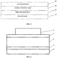
- an electroluminescent device includes sequentially: a first electrode 10, a hole injection layer 20, a hole transport layer 30, a light emitting layer 40, an electron transport layer 50, and the second electrode 60.
- the material of the electron transport layer 50 is a crosslinked nanoparticle thin film formed from crosslinking reactions.
- the material for the first electrode is selected from one or more of: indium-doped tin oxide (ITO), fluorine-doped tin oxide (FTO), antimony doped tin oxide (ATO), aluminum-doped zinc oxide (AZO); preferably, the first electrode is an ITO electrode.
- the material for the hole transport layer 430 is selected from the materials or the materials with the chemical groups: poly[bis(4-phenyl)(4-butylphenyl)amine], 4-butyl-N,N-diphenylaniline homopolymer, aniline, 4-butyl-N,N-diphenyl, homopolymer (poly-TPD), poly(9,9-dioctylfluorene-CO-N-(4-butylphenyl)-diphenylamine) (TFB), poly(9-vinylcarbazole) (PVK), TPD, Spiro-TPD, LG101, HAT-CN, PEDOT: PSS, TAPC, a-NPB, m-MTDATA, Ni x O, MoO x , VO x , WO x and a mixture thereof; preferably, the hole transport layer 30 is a poly-TPD layer and has a thickness of 10 to 100 nm.
- the material for the quantum dot light-emitting layer includes but not limited to: nanocrystals of II-VI semiconductor, for example, CdS, CdSe, CdTe, ZnS, ZnSe, ZnTe, HgS, HgSe, HgTe, PbS, PbSe, PbTe and other binary, ternary, or quaternary II-VI compounds; III-V semiconductor nanocrystals, for example, GaP, GaAs, InP, InAs or other binary, ternary, or quaternary III-V compounds.
- the quantum dot luminescent material for electroluminescence is not limited to II-V compounds, III-VI compounds, IV-VI compounds, I-III-VI compounds, II-IV-VI compound, or group IV elements.
- the material for the second electrode is selected from: Al, Ag, Cu, Mo, Au, or an alloy thereof; preferably, the material for the second electrode is Au.
- the second electrode has a thickness of 50 to 500 nm; preferably, the second electrode has a thickness of 100 to 200 nm.
- the thin film photovoltaic device includes: a first electrode 10, a light absorbing layer 20, an electron extraction layer 30, and a second electrode 40.
- the material for the electron extraction layer 30 is a crosslinked nanoparticle thin film formed by crosslinking reactions in a nanoparticle thin film.
- the first electrode and the second electrode has high sunlight transmittance.
- the first electrode is selected from one or more of: indium-doped tin oxide (ITO), fluorine-doped tin oxide (FTO), antimony-doped tin oxide (ATO), and aluminum-doped zinc oxide (AZO); preferably, the material for the first electrode is ITO.
- the light absorbing layer may be a semiconductor homojunction or a heterojunction.
- the material for the light absorbing layer is a light absorbing material in a solar spectrum, and may include: polymer photovoltaic material; organic small molecule photovoltaic material; halogen-containing perovskite photovoltaic material; chalcopyrite structural material (e.g., copper indium gallium selenide); II-VI compound material (e.g., thin films and nanocrystals); single crystal, polycrystalline, or amorphous silicon. If the light absorbing layer is a homojunction, the light absorbing layer includes a specific material of one material category from above; if the light absorbing layer is a heterojunction, the light absorbing layer includes two specific materials from one or two material categories from above.
- the material for the second electrode is selected from: Al, Ag, Cu, Mo, Au, or an alloy thereof; preferably, the material for the second electrode is Au.
- the second electrode has a thickness of 50 to 500 nm; preferably, the second electrode has a thickness of 100 to 200 nm.
- the thin film light detector includes sequentially: an anode 4, an electron blocking layer 5, a light absorbing layer 6, a hole blocking layer 7, and a cathode 8.
- the material of the hole blocking layer 7 is a crosslinked nanoparticle thin film obtained by crosslinking reactions in a nanoparticle thin film.
- At least one of the anode and the cathode has high transmittance for the detection band.
- the material for the anode is selected one or more of indium-doped tin oxide (ITO), fluorine-doped tin oxide (FTO), antimony-doped tin oxide (ATO), and aluminum-doped zinc oxide (AZO); preferably, the material for the anode is ITO.
- ITO indium-doped tin oxide
- FTO fluorine-doped tin oxide
- ATO antimony-doped tin oxide
- AZO aluminum-doped zinc oxide
- the material for the electron blocking layer is selected from: poly(9,9-dioctylfluorene-CO-N-(4-butylphenyl)-diphenylamine) (TFB), polyvinylcarbazole (PVK), poly(N,N' bis(4-butylphenyl)-N,N'-bis(phenyl)benzidine) (poly-TPD), poly(9,9-dioctylfluorene-co-bis-N,N-phenyl-1,4-phenylenediamine) (PFB), 4,4',4"-tris(carbazol-9-yl)-triphenylamine (TCTA), 4, 4'-bis(9-carbazole)-biphenyl (CBP), N,N'-diphenyl-N,N'-bis(3-methylphenyl)-1,1'-biphenyl-4, 4'-diamine (TPD), N,
- the material for the light absorbing layer is one or more of: a binary III-V compound (e.g., GaN, GaAs or InGaAs); a multinary III-V compound; a nanocrystal of a II-VI compound material, an organic semiconductor material; a halogen-containing perovskite material; a chalcopyrite structural material (e.g., copper indium gallium selenide); a single crystal, polycrystalline, or amorphous silicon.
- the light absorbing layer may be a semiconductor homojunction or a semiconductor heterojunction.
- the material for the light absorbing layer is one specific material of a material category from above.
- the material for the light absorbing layer are two specific materials of one or two material category from above.
- the cathode material is selected from: Al, Ag, Cu, Mo, Au, or an alloy thereof; preferably, the cathode material is Au.
- the cathode has a thickness of 50 to 500 nm. In some embodiments, the cathode has a thickness of 100 to 200 nm; preferably, the thin film light detector is partially packaged, fully packaged, or unpackaged.
- the semiconductor layer material of the thin film transistor is a crosslinked nanoparticle thin film formed by crosslinking reactions in a nanoparticle thin film.
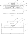
- the thin film transistor includes: a substrate 10, a source electrode 20 disposed on the substrate 10, a drain electrode 30, an insulating layer 40 disposed on the source electrode 20 and the drain electrode 30, a gate electrode 50 disposed on the insulating layer 40, and a semiconductor layer 60 disposed on the substrate 10.
- the source electrode 20 and the drain electrode 30 are separated by the semiconductor layer 60.
- the semiconductor layer 60 has a thickness greater than a thickness of the source electrode or a thickness of the drain electrode (as shown in FIG. 7a ); the semiconductor layer 60 has a thickness consistent with the thickness of the source electrode 20 or the thickness of the drain electrode 30 (as shown in FIG. 7b ).
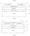
- the thin film transistor may also be configured to include: a substrate, a gate electrode, an insulating layer and a semiconductor layer, which are sequentially stacked from bottom to top.
- the semiconductor layer is configured to include a source electrode and a drain electrode; the source electrode and the drain electrode are separated from each other.
- the thin film transistor may be configured to include: a substrate, a gate electrode, an insulating layer and a semiconductor layer, which are sequentially stacked from bottom to top.
- the insulating layer is configured to include a source electrode and a drain electrode; the source electrode and the drain electrode are disposed in the interior of the semiconductor layer, and are separated by the semiconductor layer.
- the material for the source electrode, the drain electrode, and the gate electrode may be a metal or a semiconductor having high conductivity.
- the material for the insulating layer may be a dielectric material, for example, an oxide, or a nitride.
- the present disclosure provides a crosslinked nanoparticle thin film, a preparation method thereof and a thin film optoelectronic device.
- a gas mixture is introduced during the nanoparticle thin film formation, to promote crosslinking among the particles, which increases the electrical coupling between the particles, reduces the transport barrier of carriers, increases the carrier mobility, and accordingly, greatly improves the electrical performance.
- the application of the obtained crosslinked nanoparticle thin films in electroluminescent device prepared by solution methods, as electron transport layer, can apparently improve carrier balance, luminous efficiency and lifetime of the device.
- the application of the obtained crosslinked nanoparticle thin films in photovoltaic devices prepared by solution methods, as electron transport layer, can significantly reduce the linear resistance of the device, improve the parallel resistance, and improve the energy conversion efficiency of the device.
- the application of the obtained crosslinked nanoparticle thin films in thin film light detector prepared by solution methods, as electron extraction layer and hole blocking layer can reduce the current and improve the detection rate.
- the application of the obtained crosslinked nanoparticle thin films in thin film transistor prepared by solution methods can improve the carrier mobility of the semiconductor layer, increase the source-drain current, and increase the response frequency.
Landscapes
- Engineering & Computer Science (AREA)
- Chemical & Material Sciences (AREA)
- Physics & Mathematics (AREA)
- Manufacturing & Machinery (AREA)
- Nanotechnology (AREA)
- Crystallography & Structural Chemistry (AREA)
- Inorganic Chemistry (AREA)
- Electromagnetism (AREA)
- Composite Materials (AREA)
- Materials Engineering (AREA)
- Optics & Photonics (AREA)
- Photovoltaic Devices (AREA)
- Light Receiving Elements (AREA)
- Thin Film Transistor (AREA)
- Luminescent Compositions (AREA)
- Electroluminescent Light Sources (AREA)
Abstract
Description
- The present disclosure relates to the field of device film preparation, and in particular relates to a crosslinked nanoparticle film, a preparation method thereof and a film optoelectronic device.
- Oxide nanoparticles (or spherical oxide nanocrystals) have a good crystallization, which ensures their optical and electrical properties to be similar to the bulk materials (i.e., low-dimensional materials). On the other hand, the self-assembled thin films derived from nanoparticles show good performance, which allows the application of coating preparation at low cost. In the process of fabricating optoelectronic devices by solution methods, the preparation of nanoparticles is one of the important processes for corresponding oxide films to be formed. Common examples include semiconductor materials such as zinc oxide (ZnOx) nanoparticles, thin films derived from titanium oxide (TiOx) particles, which transport electrons in light-emitting diodes, thin film solar cells, thin film transistors; and semiconductor materials such as nickel oxide (NiOx) nanoparticles, which transport holes in the same device.
- Regardless, there is still a difference between thin films formed by nanoparticle deposition and thin films formed by the bulk material, which is mainly reflected on the transport properties of the carriers. Despite the good crystallinity of the interior of nanoparticles, such a structure is limited to a nanoscale; and even in the case of close-packing, nanoparticles are often filled with an insulating surface ligand or even without any fillers. Accordingly, there is a relatively high carrier transport barrier among nanoparticles, and the transport of carriers inside nanoparticle thin films can only follow the pattern of hopping transport. As a result, the carrier mobility in the dimension of thin films is much smaller than the carrier mobility in the bulk material.
- Therefore, the prior art has yet to be improved and developed.
- In view of the above deficiencies of the prior art, the present disclosure aims to provide a crosslinked nanoparticle thin film, a preparation method thereof and a thin film optoelectronic device, which aims to solve the problems of high transport barriers for carriers and low carrier mobility in thin films for existing devices.
- The technical solution of the present invention is as follows:
- A method for preparing a crosslinked nanoparticle film, comprising:
- Step A: Dispersing the nanoparticles in a solvent and uniformly mixing to obtain a nanoparticle solution;
- Step B: Forming a nanoparticle film by a solution method, and introducing a gas mixture to promote crosslinking reactions to obtain a crosslinked nanoparticle thin film.
- The method for preparing a crosslinked nanoparticle thin film, wherein the gas mixture comprises a reduced gas, oxygen, water vapor, and carbon dioxide.
- The method for preparing a crosslinked nanoparticle thin film, wherein the reduced gas bias is controlled between 1 and 100 Pa, the oxygen bias is controlled between 0 and 2×10⁴ Pa, and the water vapor bias is controlled between 0 and 2×10³ Pa, the carbon dioxide bias is controlled between 0 and 100 Pa.
- The method for preparing a crosslinked nanoparticle thin film, wherein the mass concentration of the nanoparticle solution in the step A is 1 to 100 mg/ml.
- The method for preparing a crosslinked nanoparticle thin film, wherein the nanoparticle is one or more of: an oxide nanoparticle, a sulfide nanoparticle, a selenide nanoparticle, a nitride nanoparticle, and a fluoride nanoparticle.
- The method for preparing a crosslinked nanoparticle thin film, wherein the average diameter of the nanoparticles is controlled within 5 nm.
- The method for preparing a crosslinked nanoparticle thin film, wherein the solvent is an alcohol solvent.
- The method for preparing a crosslinked nanoparticle thin film, wherein the step B specifically comprises:
- Step B1: First, placing the nanoparticle solution in a closed environment, and preparing nanoparticle thin films from the nanoparticle solution by a solution method;
- Step B2: Introducing a gas mixture into the closed environment to promote crosslinking reactions, thereby obtaining a crosslinked nanoparticle thin film.
- The method for preparing a crosslinked nanoparticle film, wherein the step B specifically comprises:
- Step B1': First placing the nanoparticle solution in an inert atmosphere, and preparing the nanoparticle thin film from the nanoparticle solution by a solution method;
- Step B2': Placing the nanoparticle thin film in a closed environment, and introducing a gas mixture into the closed environment to promote crosslinking reactions, thereby obtaining a crosslinked nanoparticle thin film.
- The method for preparing a crosslinked nanoparticle thin film, wherein the reduced gas is one of: carbon monoxide, hydrogen, and ammonia.
- The method for preparing a crosslinked nanoparticle thin film, wherein in Step B, the crosslinked nanoparticle thin film has a thickness of 15 to 60 nm.
- A crosslinked nanoparticle thin film prepared by the method for preparing a crosslinked nanoparticle thin film as described above.
- A thin film optoelectronic device comprising a crosslinked nanoparticle thin film as described above.
- The thin film optoelectronic device, wherein the thin film optoelectronic device is any one of: an electroluminescent device, a thin film photovoltaic, a thin film photodetector, and a thin film transistor.
- The thin film optoelectronic device, wherein the electroluminescent device comprises: a first electrode, a hole injection layer, a hole transport layer, a light emitting layer, an electron transport layer, and a second electrode. The material for the electron transport layer is a crosslinked nanoparticle thin film formed by the cross-linking treatment of the nanoparticle thin film.
- The thin film optoelectronic device, wherein the thin film photovoltaic device comprises: a first electrode, a light-emitting layer, an electron extraction layer, and a second electrode. The material for the electron extraction layer is a crosslinked nanoparticle thin film formed by the cross-linking treatment of the nanoparticle thin film.
- The thin film optoelectronic device, wherein the thin film light detector comprises: an anode, an electron blocking layer, a light absorbing layer, a hole blocking layer and a cathode. The material for the hole blocking layer is a crosslinked nanoparticle thin film formed by the cross-linking treatment of the nanoparticle thin film.
- The thin film optoelectronic device, wherein the material for the semiconductor layer of the thin film transistor is a crosslinked nanoparticle thin film formed by cross-linking treatment of the nanoparticle thin film. The present disclosure has the beneficial effects: In the present disclosure, the nanoparticles are crosslinked when the nanoparticle thin film is formed, so as to increase the electrical coupling among the particles, reduce the transport barrier of carriers, increase the carrier mobility, and greatly improve the electrical performance. Accordingly, the nanoparticle thin film prepared thereof can significantly improve the performance of the thin film optoelectronic device.
-
-
FIG. 1 is a schematic diagram showing the structure of an existing crosslinked zinc oxide nanoparticle thin film; -
FIG. 2 is a schematic diagram showing the structure of a crosslinked zinc oxide nanoparticle thin film prepared by the method of the present disclosure; -
FIG. 3 is a diagram showing the current-voltage curves for devices composed of ITO/NPB/MoOx/A1 with different thin films; -
FIG. 4 is a schematic structural diagram of an embodiment of a thin film electroluminescent device among the embodiments of the thin film optoelectronic devices of the present disclosure; -
FIG. 5 is a schematic structural diagram of an embodiment of a thin film photovoltaic device among the embodiments of the thin film optoelectronic devices of the present disclosure; -
FIG. 6 is a schematic structural diagram of an embodiment of a thin film light detector device among the embodiments of the thin film optoelectronic devices of the present disclosure; -
FIG. 7a is a first schematic structural diagram of an embodiment of a thin film transistor among the embodiments of the thin film optoelectronic devices of the present disclosure; -
FIG. 7b is a second schematic structural diagram of an embodiment of a thin film transistor among the embodiments of the thin film optoelectronic devices of the present disclosure; -
FIG. 8 is a third schematic structural diagram of an embodiment of a thin film transistor among the embodiments of the thin film optoelectronic devices of the present disclosure; and -
FIG. 9 is a fourth schematic structural diagram of an embodiment of a thin film transistor among the embodiments of the thin film optoelectronic devices of the present disclosure. - The present disclosure provides a crosslinked nanoparticle film, a preparation method thereof and a thin film optoelectronic device. The present disclosure will be further described in detail below in order to make the objects, technical solutions and effects of the present disclosure clear. It is understood that the specific embodiments described herein are merely illustrative examples of the present disclosure and do not limit the present disclosure.
- An embodiment of the present disclosure provides a method for preparing a crosslinked nanoparticle thin film, wherein the method includes:
Step A: Dispersing nanoparticles in a solvent and uniformly mix the nanoparticles and the solvent, to obtain a nanoparticle solution. - Specifically, the step A includes: Dispersing the nanoparticles in a solvent at a mass concentration of 1 to 100 mg/ml, mix uniformly, to obtain a nanoparticle solution used for film formation by solution methods. The nanoparticles may be one or more of wide band-gap oxide nanoparticles, sulfide nanoparticles, selenide nanoparticles, nitride nanoparticles, and fluoride nanoparticles. The oxide nanoparticles may be, but not limited to one of ZnOx (e.g., ZnO), TiOx (e.g., TiO2), etc. The sulfide nanoparticles may be, but not limited to, one of zinc sulfides and molybdenum sulfides. The selenide nanoparticles may be, but are not limited to, one of zinc selenides and lead selenides. The nitride nanoparticles may be, but not limited to, one of silicon nitrides and aluminum nitrides. The fluoride nanoparticles may be, but not limited to, one of lanthanum fluorides and sodium fluorides. In the present disclosure, the dimension of the nanoparticles may be controlled. The average diameter of the spherical nanoparticles may be limited to within 5 nm, to ensure that a sufficient amount of surface state metal atoms can participate in the reactions. The solvent may be an alcohol solvent such as a methanol, an ethanol, etc.
- Step B: Preparing nanoparticle thin films by a solution method; and introducing a gas mixture to promote cross-linking reactions to obtain crosslinked nanoparticle thin films. In the present disclosure, a solution method to deposit thin films is provided, the solution method may be spin coating, ink jet printing, spray coating, or blade coating, etc.
- Specifically, the gas mixture includes: a reduced gas, an oxygen, water vapor, and carbon dioxide. Preferably, the reduced gas (e.g., carbon monoxide, hydrogen or ammonia) bias pressure is controlled between 1 and 100 Pa; the oxygen bias pressure is controlled between 0 and 2 x 10⁴ Pa; the water vapor bias pressure is controlled between 0 and 2 x 10³ Pa; and the carbon dioxide bias pressure is controlled between 0 and 100 Pa. According to the present disclosure, the bias pressure of the gas mixture in contact with thin films is controlled. Preferably, such bias pressure of each gas is controlled within the above-described ranges, because the density of thin film prepared under such bias pressure ranges is higher, and accordingly, the carrier mobility in the thin films is also higher.
- The conditions for crosslinking reactions for each of the above type of nanoparticles will be described in detail below.
- When the nanoparticles are zinc oxide nanoparticles, the reduced gas (e.g., carbon monoxide, hydrogen or ammonia) bias pressure is controlled between 1 and 100 Pa; the oxygen bias pressure is controlled between 0 and 1×10³ Pa; the water vapor bias pressure is controlled between 0 and 2 x 10³ Pa; and the carbon dioxide bias pressure is controlled between 0 and 100 Pa. The density of thin films prepared under such bias pressure ranges is higher, and accordingly, the carrier electron mobility in the thin films is also higher.
- When the nanoparticles are titanium oxide nanoparticles, the reduced gas (e.g., carbon monoxide, hydrogen or ammonia) bias pressure is controlled between 1 and 100 Pa; the oxygen bias pressure is controlled between 0 and 1×10⁴ Pa; the water vapor bias pressure is controlled between 0 and 2 x 10³ Pa; and the carbon dioxide bias pressure is controlled between 0 and 100 Pa. The density of thin films prepared under such bias ranges is higher, and accordingly, the carrier electron mobility in the thin films is also higher.
- When the nanoparticles are nickel oxide nanoparticles, the reduced gas (e.g., carbon monoxide, hydrogen or ammonia) bias pressure is controlled between 1 and 100 Pa; and the oxygen bias pressure is controlled between 0 and 5×10³ Pa; the water vapor bias pressure is controlled between 0 and 2 x 10³ P; and the carbon dioxide bias pressure is controlled between 0 and 100 Pa. The density of thin films prepared under such bias pressure ranges is higher, and accordingly, the carrier electron mobility in the thin films is also higher.
- When the nanoparticles are zinc sulfide nanoparticles, the reduced gas (e.g., carbon monoxide, hydrogen or ammonia) bias pressure is controlled between 1 and 100 Pa; the oxygen bias pressure is controlled to be less than 0.1 Pa; the water vapor bias pressure is controlled between 0 and 2×10³ Pa; and the carbon dioxide bias pressure is controlled between 0 and 100 Pa. The density of thin films prepared under such bias pressure ranges is higher, and accordingly, the carrier electron mobility in the thin films is also higher.
- When the nanoparticles are molybdenum sulfide nanoparticles, the reduced gas (e.g., carbon monoxide, hydrogen or ammonia) bias pressure is controlled between 1 and 100 Pa; the oxygen bias pressure is controlled to be less than 0.1 Pa; the water vapor bias pressure is controlled between 0 and 2×10³ Pa; and the carbon dioxide bias pressure is controlled between 0 and 100 Pa. The density of thin film under such bias pressure ranges is higher, and accordingly, the carrier electron mobility in the thin films is also higher.
- When the nanoparticles are zinc selenide nanoparticles, the reduced gas (e.g., carbon monoxide, hydrogen or ammonia) bias pressure is controlled between 1 and 100 Pa; the oxygen bias pressure is controlled to be less than 0.1 Pa; the water vapor bias pressure is controlled between 0 and 1 × 10² Pa; and the carbon dioxide bias pressure is controlled between 0 and 10 Pa. The density of thin films produced under this bias pressure ranges is higher, and accordingly, the carrier electron mobility in the thin films is also higher.
- When the nanoparticles are lead selenide nanoparticles, the reduced gas (e.g., carbon monoxide, hydrogen or ammonia) bias pressure is controlled between 1 and 100 Pa; the oxygen bias pressure is controlled to be less than 0.1 Pa; the water vapor bias pressure is controlled to be less than 0.1 Pa, carbon dioxide bias pressure is controlled between 0 and 100 Pa. The density of thin films produced under such bias pressure ranges is higher, and accordingly, the carrier electron mobility in the thin films is also higher.
- When the nanoparticles are silicon nitride nanoparticles, the reduced gas (e.g., carbon monoxide, hydrogen or ammonia) bias pressure is controlled between 1 and 100 Pa; the oxygen bias pressure is controlled at 0.1 and 1 Pa; the water vapor bias pressure is controlled between 0 and 2 × 10³Pa; and the carbon dioxide bias pressure is controlled between 0 and 100 Pa. Additionally, the nitrogen gas bias pressure is maintained at about 1 × 10⁵ Pa. The density of thin films prepared under such bias pressure ranges is higher, and accordingly, the carrier electron mobility in thin films is also higher.
- When the nanoparticles are aluminum nitride nanoparticles, the reduced gas (e.g., carbon monoxide, hydrogen or ammonia) bias pressure is controlled between 1 and 100 Pa; the oxygen bias pressure is controlled to be less than 0.1 Pa; the water vapor bias pressure is controlled between 0 and 2 × 10³Pa; and the carbon dioxide bias pressure is controlled between 10 and 100 Pa. Additionally, the nitrogen gas bias pressure is maintained at about 1 × 10 5 Pa. The density of thin film prepared under such bias pressure ranges is higher, and accordingly, the carrier electron mobility in the thin films is also higher.
- When the nanoparticles are lanthanum fluoride nanoparticles, the reduced gas (e.g., carbon monoxide, hydrogen or ammonia) bias pressure is controlled between 1 and 100 Pa; the oxygen bias pressure is controlled to be less than 0.1 Pa; the water vapor bias pressure is controlled between 0 and 1 × 10² Pa; and the carbon dioxide bias pressure is controlled between 0 and 10 Pa. The density of thin films prepared under such bias pressure ranges is higher, and accordingly, the carrier electron mobility in the thin films is also higher.
- When the nanoparticles are sodium fluoride nanoparticles, the reduced gas (e.g., carbon monoxide, hydrogen or ammonia) bias pressure is controlled between 1 and 100 Pa; the oxygen bias pressure is controlled to be less than 0.1 Pa; the water vapor bias pressure is controlled between 0 and 2 × 10³ Pa; and the carbon dioxide bias is controlled between 10 and 100 Pa. The density of thin films prepared under such bias pressure ranges is higher, and accordingly, the carrier electron mobility in the thin films is also higher.
- In the present disclosure, the nanoparticles are crosslinked during thin film formation. Cross-links are chemical bonds that connect nanoparticles, among which there are fillers. In contrast, there is no material linked by chemical bonds between the uncrosslinked nanoparticles. The crosslinking method of the present disclosure can increase the density and carrier mobility in the corresponding thin films.
- In the present disclosure, nanoparticle films can be prepared directly from a nanoparticle solution under a non-vacuum condition. Specifically, the step B includes:
- Step B1: Placing a nanoparticle solution in a closed environment, and preparing nanoparticle thin films by a solution method; and
- Step B2: Introducing a gas mixture into the closed environment, to promote crosslinking reactions, to obtain crosslinked nanoparticles.
- In the foregoing described embodiments, nanoparticle thin films are prepared from a nanoparticle solution under a closed non-vacuum condition. The above-mentioned gas mixture is then introduced to the closed environment, to promote crosslinking reactions, to obtain crosslinked nanoparticle thin films.
- The preparation of crosslinked nanoparticle thin films of the present disclosure is not limited to the above-mentioned environment. The nanoparticle thin films can be prepared under an inert atmosphere, and then be placed in a closed environment. The closed environment is then introduced a gas mixture, to promote the crosslinking reactions, to obtain nanoparticle thin films. Specifically, the Step B includes:
- Step B1': Placing the nanoparticle solution in an inert atmosphere and preparing nanoparticle thin films by a solution method; and
- Step B2': Placing the nanoparticle thin film in a closed environment, and introducing a gas mixture into the closed environment, to promote crosslinking reactions, to obtain crosslinked nanoparticle thin films.
- In the present disclosure, after the crosslinking reactions, the crosslinked nanoparticle thin films are dried to finally obtain crosslinked nanoparticle thin film having a thickness of 15 to 60 nm. The drying temperature is higher than the boiling point of the solvent in the nanoparticle solution; according to the thickness of the film, the drying time is more than 15 minutes per 50 nm.
- The present disclosure also provides a crosslinked nanoparticle thin films prepared by any of the above methods for preparing crosslinked nanoparticle thin films.
- Usually, a nanoparticle thin film is self-assembled from nanoparticles that are not crosslinked to each other. In the present disclosure, during thin film formation of the nanoparticles, a gas mixture is introduced to promote crosslinking among the particles, thereby increasing electrical coupling between the particles, reducing the transport barrier of carriers, increasing carrier mobility, and accordingly, improving the electrical performance. The application of the obtained crosslinked nanoparticle thin films in light-emitting diodes, thin film solar cells, light detectors, and thin film transistors prepared by solution methods can significantly improve the performance of these devices.
- Below is an illustrative example of zinc oxide nanoparticles, and the properties of the existing uncrosslinked zinc oxide nanoparticle thin films and the properties of the crosslinked zinc oxide nanoparticle thin films prepared by the methods of the present disclosure are tested. Referring to
FIGs.1-3 ,FIG. 1 is a schematic diagram of the structure of an existing uncrosslinked zinc oxide nanoparticle thin film,FIG. 2 is a schematic diagram of the structure of a crosslinked zinc oxide nanoparticle thin film prepared by a method of the present disclosure,FIG. 3 is a diagram showing the current-voltage curves for ITO/NPB/MoOx/A1 devices with different thin films. As shown inFIG. 1 , there is no substance connected by chemical bonds between theuncrosslinked nanoparticles 1. It can be seen inFIG. 2 , there arefillers 3 amongnanoparticles 2, andnanoparticles 2 are connected by chemical bonds. Since the added zinc oxide has an effective inhibition on the current of the devices composed of ITO/NPB/MoOx/Al structure, it can be determined whether the ZnO nanoparticle thin film may detach during the soaking process by observing whether the current is increased. As shown inFIG. 3 , the current of the crosslinked ZnO nanoparticle thin film is kept at a low value regardless of whether it is soaked in an alcohol solvent (e.g., ethanol), which indicates that ZnO nanoparticle thin film does not detach during soaking, which results in an apparent inhibitory effect on the current of the ITO/NPB/MoOx/Al structure by ZnO. However, the current is significantly increased when the uncrosslinked ZnO nanoparticle thin film is soaked in an alcohol solvent (e.g., ethanol), which indicates that the uncrosslinked ZnO nanoparticle thin film detaches during soaking, so that the current of the responsive devices is significantly increased, very close to the current of the devices without adding ZnO nanoparticle thin film. Therefore, the crosslinked zinc oxide nanoparticle thin film obtained by crosslinking reactions does not dissolve or have any detachment after soaking in the original solvent (e.g., a solvent used for dispersing zinc oxide nanoparticles, usually, i.e., an alcohol solvent). On the contrary, the uncrosslinked nanoparticle thin film can easily detach after soaking. - The present disclosure also provides a thin film optoelectronic device, wherein, the thin film optoelectronic device includes a crosslinked nanoparticle thin film. Specifically, the thin film optoelectronic device is any one of: an electroluminescent device, a thin film photovoltaic device, a thin film light detector, and a thin film transistor.
- As a specific embodiment of the optoelectronic thin film device, as shown in
FIG. 4 , an electroluminescent device includes sequentially: afirst electrode 10, ahole injection layer 20, ahole transport layer 30, alight emitting layer 40, anelectron transport layer 50, and thesecond electrode 60. The material of theelectron transport layer 50 is a crosslinked nanoparticle thin film formed from crosslinking reactions. - In the electroluminescent device of the present embodiment, at least one of the first electrode and the second electrode has high light transmittance for a light band emitted by the light emitting layer. Specifically, the material for the first electrode is selected from one or more of: indium-doped tin oxide (ITO), fluorine-doped tin oxide (FTO), antimony doped tin oxide (ATO), aluminum-doped zinc oxide (AZO); preferably, the first electrode is an ITO electrode.
- Further, in the present embodiment, the material for the hole transport layer 430 is selected from the materials or the materials with the chemical groups: poly[bis(4-phenyl)(4-butylphenyl)amine], 4-butyl-N,N-diphenylaniline homopolymer, aniline, 4-butyl-N,N-diphenyl, homopolymer (poly-TPD), poly(9,9-dioctylfluorene-CO-N-(4-butylphenyl)-diphenylamine) (TFB), poly(9-vinylcarbazole) (PVK), TPD, Spiro-TPD, LG101, HAT-CN, PEDOT: PSS, TAPC, a-NPB, m-MTDATA, NixO, MoOx, VOx, WOx and a mixture thereof; preferably, the
hole transport layer 30 is a poly-TPD layer and has a thickness of 10 to 100 nm. - Further, in the present embodiment, the material for the quantum dot light-emitting layer includes but not limited to: nanocrystals of II-VI semiconductor, for example, CdS, CdSe, CdTe, ZnS, ZnSe, ZnTe, HgS, HgSe, HgTe, PbS, PbSe, PbTe and other binary, ternary, or quaternary II-VI compounds; III-V semiconductor nanocrystals, for example, GaP, GaAs, InP, InAs or other binary, ternary, or quaternary III-V compounds. The quantum dot luminescent material for electroluminescence is not limited to II-V compounds, III-VI compounds, IV-VI compounds, I-III-VI compounds, II-IV-VI compound, or group IV elements.
- Further, in the present embodiment, the material for the second electrode is selected from: Al, Ag, Cu, Mo, Au, or an alloy thereof; preferably, the material for the second electrode is Au. The second electrode has a thickness of 50 to 500 nm; preferably, the second electrode has a thickness of 100 to 200 nm.
- As a specific embodiment of the thin film optoelectronic device, as shown in
FIG. 5 , the thin film photovoltaic device includes: afirst electrode 10, alight absorbing layer 20, anelectron extraction layer 30, and asecond electrode 40. The material for theelectron extraction layer 30 is a crosslinked nanoparticle thin film formed by crosslinking reactions in a nanoparticle thin film. - In the present embodiment of the thin film photovoltaic device, at least one of the first electrode and the second electrode has high sunlight transmittance. Specifically, the first electrode is selected from one or more of: indium-doped tin oxide (ITO), fluorine-doped tin oxide (FTO), antimony-doped tin oxide (ATO), and aluminum-doped zinc oxide (AZO); preferably, the material for the first electrode is ITO.
- Further, according to the present embodiment, the light absorbing layer may be a semiconductor homojunction or a heterojunction. The material for the light absorbing layer is a light absorbing material in a solar spectrum, and may include: polymer photovoltaic material; organic small molecule photovoltaic material; halogen-containing perovskite photovoltaic material; chalcopyrite structural material (e.g., copper indium gallium selenide); II-VI compound material (e.g., thin films and nanocrystals); single crystal, polycrystalline, or amorphous silicon. If the light absorbing layer is a homojunction, the light absorbing layer includes a specific material of one material category from above; if the light absorbing layer is a heterojunction, the light absorbing layer includes two specific materials from one or two material categories from above.
- Further, in the present embodiment, the material for the second electrode is selected from: Al, Ag, Cu, Mo, Au, or an alloy thereof; preferably, the material for the second electrode is Au. The second electrode has a thickness of 50 to 500 nm; preferably, the second electrode has a thickness of 100 to 200 nm.
- As a specific embodiment of the thin film optoelectronic device, as shown in
FIG. 6 , the thin film light detector includes sequentially: ananode 4, anelectron blocking layer 5, alight absorbing layer 6, ahole blocking layer 7, and acathode 8. The material of thehole blocking layer 7 is a crosslinked nanoparticle thin film obtained by crosslinking reactions in a nanoparticle thin film. - According to the present embodiment of the thin film light detector, at least one of the anode and the cathode has high transmittance for the detection band.
- Further, in the present embodiment, the material for the anode is selected one or more of indium-doped tin oxide (ITO), fluorine-doped tin oxide (FTO), antimony-doped tin oxide (ATO), and aluminum-doped zinc oxide (AZO); preferably, the material for the anode is ITO.
- Further, in the present embodiment, the material for the electron blocking layer is selected from: poly(9,9-dioctylfluorene-CO-N-(4-butylphenyl)-diphenylamine) (TFB), polyvinylcarbazole (PVK), poly(N,N' bis(4-butylphenyl)-N,N'-bis(phenyl)benzidine) (poly-TPD), poly(9,9-dioctylfluorene-co-bis-N,N-phenyl-1,4-phenylenediamine) (PFB), 4,4',4"-tris(carbazol-9-yl)-triphenylamine (TCTA), 4, 4'-bis(9-carbazole)-biphenyl (CBP), N,N'-diphenyl-N,N'-bis(3-methylphenyl)-1,1'-biphenyl-4, 4'-diamine (TPD), N,N'-diphenyl-N,N'-(1-naphthyl)-1,1'-biphenyl-4,4'-diamine (NPB), doped graphene, undoped graphene, C60, or a mixture thereof; preferably, the material for the
electron blocking layer 5 is poly-TPD. The electron blocking layer 620 has a thickness of 10 to 100 nm. - Further, in the present embodiment, the material for the light absorbing layer is one or more of: a binary III-V compound (e.g., GaN, GaAs or InGaAs); a multinary III-V compound; a nanocrystal of a II-VI compound material, an organic semiconductor material; a halogen-containing perovskite material; a chalcopyrite structural material (e.g., copper indium gallium selenide); a single crystal, polycrystalline, or amorphous silicon. The light absorbing layer (photoelectron generating layer) may be a semiconductor homojunction or a semiconductor heterojunction. Specifically, in some embodiments, if the light absorbing layer is a homojunction, the material for the light absorbing layer is one specific material of a material category from above. Specifically, if the light absorbing layer is a heterojunction, the material for the light absorbing layer are two specific materials of one or two material category from above.
- Further, in the present embodiment, the cathode material is selected from: Al, Ag, Cu, Mo, Au, or an alloy thereof; preferably, the cathode material is Au. The cathode has a thickness of 50 to 500 nm. In some embodiments, the cathode has a thickness of 100 to 200 nm; preferably, the thin film light detector is partially packaged, fully packaged, or unpackaged.
- As a specific embodiment of the thin film optoelectronic device, as shown in
FIG. 7a , the semiconductor layer material of the thin film transistor is a crosslinked nanoparticle thin film formed by crosslinking reactions in a nanoparticle thin film. The thin film transistor includes: asubstrate 10, asource electrode 20 disposed on thesubstrate 10, adrain electrode 30, an insulatinglayer 40 disposed on thesource electrode 20 and thedrain electrode 30, agate electrode 50 disposed on the insulatinglayer 40, and asemiconductor layer 60 disposed on thesubstrate 10. Thesource electrode 20 and thedrain electrode 30 are separated by thesemiconductor layer 60. Specifically, thesemiconductor layer 60 has a thickness greater than a thickness of the source electrode or a thickness of the drain electrode (as shown inFIG. 7a ); thesemiconductor layer 60 has a thickness consistent with the thickness of thesource electrode 20 or the thickness of the drain electrode 30 (as shown inFIG. 7b ). - Further, as shown in
FIG. 8 , the thin film transistor may also be configured to include: a substrate, a gate electrode, an insulating layer and a semiconductor layer, which are sequentially stacked from bottom to top. The semiconductor layer is configured to include a source electrode and a drain electrode; the source electrode and the drain electrode are separated from each other. - Or, as shown in
FIG. 9 , the thin film transistor may be configured to include: a substrate, a gate electrode, an insulating layer and a semiconductor layer, which are sequentially stacked from bottom to top. The insulating layer is configured to include a source electrode and a drain electrode; the source electrode and the drain electrode are disposed in the interior of the semiconductor layer, and are separated by the semiconductor layer. - In the present embodiment of the thin film transistor, the material for the source electrode, the drain electrode, and the gate electrode may be a metal or a semiconductor having high conductivity. The material for the insulating layer may be a dielectric material, for example, an oxide, or a nitride.
- In summary, the present disclosure provides a crosslinked nanoparticle thin film, a preparation method thereof and a thin film optoelectronic device. In the present disclosure, a gas mixture is introduced during the nanoparticle thin film formation, to promote crosslinking among the particles, which increases the electrical coupling between the particles, reduces the transport barrier of carriers, increases the carrier mobility, and accordingly, greatly improves the electrical performance. The application of the obtained crosslinked nanoparticle thin films in electroluminescent device prepared by solution methods, as electron transport layer, can apparently improve carrier balance, luminous efficiency and lifetime of the device. The application of the obtained crosslinked nanoparticle thin films in photovoltaic devices prepared by solution methods, as electron transport layer, can significantly reduce the linear resistance of the device, improve the parallel resistance, and improve the energy conversion efficiency of the device. The application of the obtained crosslinked nanoparticle thin films in thin film light detector prepared by solution methods, as electron extraction layer and hole blocking layer, can reduce the current and improve the detection rate. The application of the obtained crosslinked nanoparticle thin films in thin film transistor prepared by solution methods, can improve the carrier mobility of the semiconductor layer, increase the source-drain current, and increase the response frequency.
It is to be understood that the application of the present disclosure is not limited to the foregoing described examples, and those skilled in the art can make modifications and variations in accordance with the above descriptions, all of which are within the scope of the appended claims.
Claims (18)
- A method for preparing crosslinked nanoparticle thin film, wherein, comprising:step A: dispersing nanoparticles in a solvent and uniformly mixing to obtain a nanoparticle solution;step B: preparing a nanoparticle thin film from the nanoparticle solution by a solution method, and introducing a gas mixture to promote crosslinking reactions, to obtain crosslinked nanoparticle thin film.
- The method for preparing crosslinked nanoparticle thin film according to claim 1, wherein the gas mixture comprises a reduced gas, oxygen, water vapor and carbon dioxide.
- The method for preparing crosslinked nanoparticle thin film according to claim 2, wherein a bias pressure for the reduced gas is controlled between 1 and 100 Pa, a bias pressure for the oxygen is controlled between 0 and 2 x 10⁴ Pa, a bias pressure for the water vapor is controlled between 0 and 2 x 10³ Pa, and a bias pressure for the carbon dioxide is controlled between 0 and 100 Pa.
- The method for preparing crosslinked nanoparticle thin film according to claim 1, wherein in the step A, the nanoparticle solution has a mass concentration of 1 to 100 mg/ml.
- The method for preparing crosslinked nanoparticle thin film according to claim 1, wherein the nanoparticles are one or more of: oxide nanoparticles, sulfide nanoparticles, selenide nanoparticles, nitride nanoparticles, and fluoride nanoparticles.
- The method for preparing crosslinked nanoparticle thin film according to claim 1, wherein an average diameter of the nanoparticles is controlled within 5 nm.
- The method for preparing crosslinked nanoparticle thin film according to claim 1, wherein the solvent is an alcohol solvent.
- The method for preparing crosslinked nanoparticle thin film according to claim 1, wherein the step B comprises:step B1: first placing the nanoparticle solution in a closed environment, and preparing nanoparticle thin film from the nanoparticle solution by the solution method;step B2: then introducing a gas mixture to the closed environment to promote crosslinking reactions, to obtain crosslinked nanoparticle thin film.
- The method for preparing crosslinked nanoparticle thin film according to claim 1, wherein the step B comprises:step B1: first placing the nanoparticle solution in an inert atmosphere, and preparing nanoparticle thin film from the nanoparticle solution by the solution method;step B2: then placing the nanoparticle thin film in a closed environment, introducing a gas mixture to the closed environment to promote crosslinking reactions, to obtain crosslinked nanoparticle thin film.
- The method for preparing crosslinked nanoparticle thin film according to claim 2, wherein the reduced gas is one of: carbon monoxide, hydrogen, and ammonia.
- The method for preparing crosslinked nanoparticle thin film according to claim 1, wherein the crosslinked nanoparticle film has a thickness of 15 to 60 nm.
- A crosslinked nanoparticle thin film, wherein, prepared by the method for preparing crosslinked nanoparticle thin film according to any one of claims 1 to 11.
- A thin film optoelectronic device, wherein, comprising a crosslinked nanoparticle thin film prepared by the method according to claim 12.
- The thin film optoelectronic device according to claim 13, wherein the thin film optoelectronic device is any one of: an electroluminescent device, a thin film photovoltaic, a thin film light detector, and a thin film transistor.
- The thin film optoelectronic device according to claim 14, wherein the electroluminescent device comprises: a first electrode, a hole injection layer, a hole transport layer, a light emitting layer, an electron transport layer and a second electrode; a material for the electron transport layer is the crosslinked nanoparticle thin film formed by crosslinking treatment of the nanoparticle thin film.
- The thin film optoelectronic device according to claim 14, wherein the thin film photovoltaic device comprises: a first electrode, a light absorbing layer, an electron extraction layer and a second electrode; a material for the electron extraction layer is the crosslinked nanoparticle thin film formed by crosslinking treatment of the nanoparticle thin film.
- The thin film optoelectronic device according to claim 14, wherein the light detector device comprises: an anode, an electron blocking layer, a hole blocking layer and a cathode; a material for the hole blocking layer is the crosslinked nanoparticle thin film formed by crosslinking treatment of the nanoparticle thin film.
- The thin film optoelectronic device according to claim 14, wherein a material for a semiconductor layer of the thin film transistor is the crosslinked nanoparticle thin film formed by crosslinking treatment of the nanoparticle thin film.
Applications Claiming Priority (6)
| Application Number | Priority Date | Filing Date | Title |
|---|---|---|---|
| CN201710232917.8A CN108695406B (en) | 2017-04-11 | 2017-04-11 | A kind of thin film photodetector and preparation method thereof |
| CN201710232650.2A CN108695376B (en) | 2017-04-11 | 2017-04-11 | A kind of thin film transistor and its preparation method |
| CN201710233270.0A CN108695137B (en) | 2017-04-11 | 2017-04-11 | Cross-linked nano-particle film, preparation method thereof and film optoelectronic device |
| CN201710232910.6A CN108695405B (en) | 2017-04-11 | 2017-04-11 | A kind of thin film photovoltaic device and its preparation method |
| CN201710232916.3A CN108695413B (en) | 2017-04-11 | 2017-04-11 | A kind of electroluminescent device and preparation method thereof |
| PCT/CN2018/079025 WO2018188448A1 (en) | 2017-04-11 | 2018-03-14 | Crosslinked nanoparticle thin film and preparation method therefor, and thin film optoelectronic device |
Publications (2)
| Publication Number | Publication Date |
|---|---|
| EP3611756A1 true EP3611756A1 (en) | 2020-02-19 |
| EP3611756A4 EP3611756A4 (en) | 2020-12-30 |
Family
ID=63793644
Family Applications (1)
| Application Number | Title | Priority Date | Filing Date |
|---|---|---|---|
| EP18784835.3A Ceased EP3611756A4 (en) | 2017-04-11 | 2018-03-14 | CROSSLINKED NANOPARTICLE THIN-FILM AND MANUFACTURING METHOD FOR IT AS WELL AS OPTOELECTRONIC THIN-FILM DEVICE |
Country Status (5)
| Country | Link |
|---|---|
| US (2) | US20200313089A1 (en) |
| EP (1) | EP3611756A4 (en) |
| JP (1) | JP7075476B2 (en) |
| KR (1) | KR102260236B1 (en) |
| WO (1) | WO2018188448A1 (en) |
Families Citing this family (3)
| Publication number | Priority date | Publication date | Assignee | Title |
|---|---|---|---|---|
| CN112909116B (en) * | 2021-01-18 | 2023-08-04 | 华中科技大学 | A Field Effect Transistor Photodetector Based on Dielectric Layer Response |
| CN116018033A (en) * | 2021-10-20 | 2023-04-25 | Tcl科技集团股份有限公司 | Preparation method of QLED device, display substrate, and display device |
| TR2023018679A2 (en) * | 2023-12-27 | 2024-07-22 | Tuerkiye Garanti Bankasi Anonim Sirketi | A SYSTEM THAT ALLOWS BUSINESS ANALYSIS |
Family Cites Families (26)
| Publication number | Priority date | Publication date | Assignee | Title |
|---|---|---|---|---|
| JP2005045188A (en) | 2003-07-25 | 2005-02-17 | Fuji Xerox Co Ltd | Electronic device, integrated circuit and manufacturing method thereof |
| KR101243917B1 (en) | 2005-12-19 | 2013-03-14 | 삼성디스플레이 주식회사 | A conducting polymer composition and an electrical device employing the layer obtained from the conducting polymer composition |
| JP4806320B2 (en) | 2006-09-21 | 2011-11-02 | 株式会社神戸製鋼所 | Substrate coating method and surface-coated substrate |
| JP5222486B2 (en) | 2007-04-11 | 2013-06-26 | 株式会社アルバック | Method for forming transparent conductive film |
| JP2010010175A (en) * | 2008-06-24 | 2010-01-14 | Konica Minolta Holdings Inc | Thin film transistor, and method of manufacturing thin film transistor |
| US20100006837A1 (en) * | 2008-07-09 | 2010-01-14 | Electronics And Telecommunications Research Institute | Composition for oxide semiconductor thin film, field effect transistor using the composition and method of fabricating the transistor |
| JP2013504186A (en) | 2009-09-05 | 2013-02-04 | メルク パテント ゲゼルシャフト ミット ベシュレンクテル ハフツング | Solution processable passivation layers for organic electronic devices |
| US20120256166A1 (en) | 2009-12-17 | 2012-10-11 | Merck Patent Gesellschaft Mit Beschrankter Haftung | Deposition of nanoparticles |
| KR101100959B1 (en) | 2010-03-10 | 2011-12-29 | 삼성모바일디스플레이주식회사 | A display device including a thin film transistor, a method of manufacturing the same, and a thin film transistor |
| US8536105B2 (en) | 2010-06-08 | 2013-09-17 | Innovation Services, Inc. | Method of cleaning contaminated surfaces |
| BR112013012728A2 (en) | 2010-11-23 | 2016-09-13 | Nanoholdings Llc | "High detectivity infrared photodetectors on low voltage device." |
| JP5916761B2 (en) | 2011-01-28 | 2016-05-11 | ノースウェスタン ユニバーシティ | Low temperature fabrication of metal composite thin films derived from metal oxide thin films and nanomaterials |
| JP2013062185A (en) | 2011-09-14 | 2013-04-04 | Ulvac Japan Ltd | Transparent conductive film forming method |
| JP5900846B2 (en) | 2011-11-18 | 2016-04-06 | 国立研究開発法人産業技術総合研究所 | Nano ink applicator |
| AU2013315518B2 (en) * | 2012-09-17 | 2017-11-09 | Eastman Chemical Company | Methods, materials and apparatus for improving control and efficiency of layer-by-layer processes |
| WO2014099080A2 (en) | 2012-09-26 | 2014-06-26 | University Of Florida Research Foundation, Inc. | Transparent quantum dot light-emitting diodes with dielectric/metal/dielectric electrode |
| KR20150109325A (en) * | 2012-10-18 | 2015-10-01 | 테라-배리어 필름스 피티이 리미티드 | Encapsulation barrier stack |
| CN102909005B (en) * | 2012-10-24 | 2014-02-05 | 中国科学院理化技术研究所 | Graphene-based composite material with surface coated with mesoporous silica and loaded with precious metal nanoparticles, and preparation method and application thereof |
| CN102931289B (en) * | 2012-11-28 | 2015-05-13 | 山东力诺太阳能电力股份有限公司 | Preparation method of flower piece solar cell |
| KR20160078954A (en) | 2013-08-29 | 2016-07-05 | 유니버시티 오브 플로리다 리서치 파운데이션, 아이엔씨. | Air stable infrared photodetectors from solution-processed inorganic semiconductors |
| CN103681886B (en) * | 2013-12-26 | 2017-09-22 | 中国科学院物理研究所 | Shelf layer for perovskite-based thin film solar cell and preparation method thereof |
| JPWO2015190335A1 (en) | 2014-06-11 | 2017-04-20 | コニカミノルタ株式会社 | Phototherapy device |
| JP6052326B2 (en) | 2015-04-15 | 2016-12-27 | コニカミノルタ株式会社 | Organic electroluminescence element, display device and lighting device |
| CA2988784A1 (en) * | 2015-06-11 | 2017-03-09 | University Of Florida Research Foundation, Incorporated | Monodisperse, ir-absorbing nanoparticles and related methods and devices |
| JP6074777B2 (en) | 2015-07-06 | 2017-02-08 | 国立研究開発法人産業技術総合研究所 | Nano ink applicator |
| CN108695413B (en) | 2017-04-11 | 2019-11-12 | Tcl集团股份有限公司 | A kind of electroluminescent device and preparation method thereof |
-
2018
- 2018-03-14 JP JP2020502747A patent/JP7075476B2/en active Active
- 2018-03-14 KR KR1020197028863A patent/KR102260236B1/en active Active
- 2018-03-14 US US16/603,772 patent/US20200313089A1/en not_active Abandoned
- 2018-03-14 WO PCT/CN2018/079025 patent/WO2018188448A1/en not_active Ceased
- 2018-03-14 EP EP18784835.3A patent/EP3611756A4/en not_active Ceased
-
2022
- 2022-07-27 US US17/874,934 patent/US11778891B2/en active Active
Also Published As
| Publication number | Publication date |
|---|---|
| US20220367812A1 (en) | 2022-11-17 |
| JP2020516045A (en) | 2020-05-28 |
| JP7075476B2 (en) | 2022-05-25 |
| WO2018188448A1 (en) | 2018-10-18 |
| KR102260236B1 (en) | 2021-06-03 |
| US11778891B2 (en) | 2023-10-03 |
| KR20190117778A (en) | 2019-10-16 |
| EP3611756A4 (en) | 2020-12-30 |
| US20200313089A1 (en) | 2020-10-01 |
Similar Documents
| Publication | Publication Date | Title |
|---|---|---|
| US11309138B2 (en) | Contact passivation for perovskite optoelectronics | |
| US11778891B2 (en) | Crosslinked nanoparticle thin film, preparation method thereof, and thin film optoelectronic device having the same | |
| EP2483926B1 (en) | Quantum dot-fullerene junction optoelectronic devices | |
| CN105900529B (en) | Light emitting device and method for manufacturing light emitting device | |
| US20150263203A1 (en) | Intermediate band semiconductors, heterojunctions, and optoelectronic devices utilizing solution processed quantum dots, and related methods | |
| EP3308113A2 (en) | Monodisperse, ir-absorbing nanoparticles and related methods and devices | |
| US9006931B2 (en) | Static-electrical-field-enhanced semiconductor-based devices and methods of enhancing semiconductor-based device performance | |
| CN108695413B (en) | A kind of electroluminescent device and preparation method thereof | |
| Ramar et al. | Study of Schottky contact in binary and ternary hybrid CdSe quantum dot solar cells | |
| KR20130113455A (en) | Organic semiconductors as window layers for inorganic solar cells | |
| CN110649168B (en) | Quantum dot light-emitting diode and preparation method thereof | |
| US20120319083A1 (en) | Nanorod semiconductor device having a contact structure, and method for manufacturing same | |
| CN113046077B (en) | Composite material, quantum dot light-emitting diode and preparation method thereof | |
| CN119096372A (en) | Photovoltaic device and manufacturing method | |
| CN108695406A (en) | A kind of thin-film photodetector and preparation method thereof | |
| He et al. | Crystallographic and Stoichiometric Control of ALD‐SnO2 Interconnects for Efficient Flexible Perovskite‐organic‐tandem Photovoltaics | |
| CN117623369B (en) | Symmetric doping methods for zinc-based oxide semiconductor nanocrystals and their applications | |
| CN112397660B (en) | Nano material and preparation method and application thereof | |
| CN108695405B (en) | A kind of thin film photovoltaic device and its preparation method | |
| CN114267799A (en) | Quantum dot light-emitting diode and preparation method thereof | |
| CN115377300A (en) | Electron transport material and preparation method thereof, and display device and preparation method thereof | |
| CN114695697A (en) | Quantum dot light-emitting diode and preparation method thereof | |
| CN113054143A (en) | Nano material, preparation method thereof and quantum dot light-emitting diode | |
| Bernède | Organic photovoltaic cells: engineering of the interfaces electrodes/organic material |
Legal Events
| Date | Code | Title | Description |
|---|---|---|---|
| STAA | Information on the status of an ep patent application or granted ep patent |
Free format text: STATUS: THE INTERNATIONAL PUBLICATION HAS BEEN MADE |
|
| PUAI | Public reference made under article 153(3) epc to a published international application that has entered the european phase |
Free format text: ORIGINAL CODE: 0009012 |
|
| STAA | Information on the status of an ep patent application or granted ep patent |
Free format text: STATUS: REQUEST FOR EXAMINATION WAS MADE |
|
| 17P | Request for examination filed |
Effective date: 20190930 |
|
| AK | Designated contracting states |
Kind code of ref document: A1 Designated state(s): AL AT BE BG CH CY CZ DE DK EE ES FI FR GB GR HR HU IE IS IT LI LT LU LV MC MK MT NL NO PL PT RO RS SE SI SK SM TR |
|
| AX | Request for extension of the european patent |
Extension state: BA ME |
|
| RAP1 | Party data changed (applicant data changed or rights of an application transferred) |
Owner name: TCL TECHNOLOGY GROUP CORPORATION |
|
| DAV | Request for validation of the european patent (deleted) | ||
| DAX | Request for extension of the european patent (deleted) | ||
| REG | Reference to a national code |
Ref country code: DE Ref legal event code: R079 Free format text: PREVIOUS MAIN CLASS: H01L0021020000 Ipc: H01L0031180000 |
|
| A4 | Supplementary search report drawn up and despatched |
Effective date: 20201130 |
|
| RIC1 | Information provided on ipc code assigned before grant |
Ipc: H01L 51/50 20060101ALI20201124BHEP Ipc: H01L 31/18 20060101AFI20201124BHEP Ipc: H01L 33/00 20100101ALI20201124BHEP Ipc: H01L 51/42 20060101ALI20201124BHEP |
|
| STAA | Information on the status of an ep patent application or granted ep patent |
Free format text: STATUS: EXAMINATION IS IN PROGRESS |
|
| 17Q | First examination report despatched |
Effective date: 20230112 |
|
| REG | Reference to a national code |
Ref country code: DE Ref legal event code: R003 |
|
| STAA | Information on the status of an ep patent application or granted ep patent |
Free format text: STATUS: THE APPLICATION HAS BEEN REFUSED |
|
| 18R | Application refused |
Effective date: 20250923 |