EP3610489B1 - An integrated transformer - Google Patents
An integrated transformer Download PDFInfo
- Publication number
- EP3610489B1 EP3610489B1 EP17716531.3A EP17716531A EP3610489B1 EP 3610489 B1 EP3610489 B1 EP 3610489B1 EP 17716531 A EP17716531 A EP 17716531A EP 3610489 B1 EP3610489 B1 EP 3610489B1
- Authority
- EP
- European Patent Office
- Prior art keywords
- winding
- internal node
- transformer
- inductor
- branch
- Prior art date
- Legal status (The legal status is an assumption and is not a legal conclusion. Google has not performed a legal analysis and makes no representation as to the accuracy of the status listed.)
- Active
Links
Images





Classifications
-
- H—ELECTRICITY
- H01—ELECTRIC ELEMENTS
- H01F—MAGNETS; INDUCTANCES; TRANSFORMERS; SELECTION OF MATERIALS FOR THEIR MAGNETIC PROPERTIES
- H01F19/00—Fixed transformers or mutual inductances of the signal type
- H01F19/04—Transformers or mutual inductances suitable for handling frequencies considerably beyond the audio range
-
- H—ELECTRICITY
- H01—ELECTRIC ELEMENTS
- H01F—MAGNETS; INDUCTANCES; TRANSFORMERS; SELECTION OF MATERIALS FOR THEIR MAGNETIC PROPERTIES
- H01F27/00—Details of transformers or inductances, in general
- H01F27/28—Coils; Windings; Conductive connections
- H01F27/2804—Printed windings
-
- H—ELECTRICITY
- H03—ELECTRONIC CIRCUITRY
- H03F—AMPLIFIERS
- H03F3/00—Amplifiers with only discharge tubes or only semiconductor devices as amplifying elements
- H03F3/189—High-frequency amplifiers, e.g. radio frequency amplifiers
- H03F3/19—High-frequency amplifiers, e.g. radio frequency amplifiers with semiconductor devices only
- H03F3/195—High-frequency amplifiers, e.g. radio frequency amplifiers with semiconductor devices only in integrated circuits
-
- H—ELECTRICITY
- H03—ELECTRONIC CIRCUITRY
- H03F—AMPLIFIERS
- H03F3/00—Amplifiers with only discharge tubes or only semiconductor devices as amplifying elements
- H03F3/20—Power amplifiers, e.g. Class B amplifiers, Class C amplifiers
- H03F3/21—Power amplifiers, e.g. Class B amplifiers, Class C amplifiers with semiconductor devices only
- H03F3/211—Power amplifiers, e.g. Class B amplifiers, Class C amplifiers with semiconductor devices only using a combination of several amplifiers
-
- H—ELECTRICITY
- H03—ELECTRONIC CIRCUITRY
- H03F—AMPLIFIERS
- H03F3/00—Amplifiers with only discharge tubes or only semiconductor devices as amplifying elements
- H03F3/20—Power amplifiers, e.g. Class B amplifiers, Class C amplifiers
- H03F3/24—Power amplifiers, e.g. Class B amplifiers, Class C amplifiers of transmitter output stages
- H03F3/245—Power amplifiers, e.g. Class B amplifiers, Class C amplifiers of transmitter output stages with semiconductor devices only
-
- H—ELECTRICITY
- H03—ELECTRONIC CIRCUITRY
- H03F—AMPLIFIERS
- H03F3/00—Amplifiers with only discharge tubes or only semiconductor devices as amplifying elements
- H03F3/45—Differential amplifiers
- H03F3/45071—Differential amplifiers with semiconductor devices only
- H03F3/45076—Differential amplifiers with semiconductor devices only characterised by the way of implementation of the active amplifying circuit in the differential amplifier
- H03F3/45475—Differential amplifiers with semiconductor devices only characterised by the way of implementation of the active amplifying circuit in the differential amplifier using IC blocks as the active amplifying circuit
-
- H—ELECTRICITY
- H03—ELECTRONIC CIRCUITRY
- H03F—AMPLIFIERS
- H03F2200/00—Indexing scheme relating to amplifiers
- H03F2200/541—Transformer coupled at the output of an amplifier
-
- H—ELECTRICITY
- H03—ELECTRONIC CIRCUITRY
- H03F—AMPLIFIERS
- H03F2203/00—Indexing scheme relating to amplifiers with only discharge tubes or only semiconductor devices as amplifying elements covered by H03F3/00
- H03F2203/45—Indexing scheme relating to differential amplifiers
- H03F2203/45228—A transformer being added at the output or the load circuit of the dif amp
-
- H—ELECTRICITY
- H03—ELECTRONIC CIRCUITRY
- H03F—AMPLIFIERS
- H03F2203/00—Indexing scheme relating to amplifiers with only discharge tubes or only semiconductor devices as amplifying elements covered by H03F3/00
- H03F2203/45—Indexing scheme relating to differential amplifiers
- H03F2203/45731—Indexing scheme relating to differential amplifiers the LC comprising a transformer
Definitions
- Embodiments herein relate to an integrated transformer arrangement.
- they relate to an integrated transformer arrangement for combining output signals of multiple differential amplifiers to a single-ended load, and a power amplifier and an electronic device comprising the integrated transformer arrangement.
- CMOS Complementary Metal Oxide Semiconductor
- a key part of a high performance millimeter wave power amplifier in low cost technology is combining network.
- a combining network should be able to both combine output powers or signals of several power amplifiers with very low loss and show same impedance to all incoming signals. If the impedance of the combining network seen by the power amplifiers is different, the power amplifiers will not be able to deliver the same output power. Then some of the power amplifiers will be subjected to higher voltages than others, which will cause reliability concerns. In addition, distortion generation will also increase.
- a key problem in the combination network is that balun functionality is needed. This is due to that power amplifiers integrated on a chip are preferably in differential structure and output differential signals, while a single-ended signal to an antenna is typically desired.
- FIG. 1 shows such a combination network, presented in A. Tuffery, et. al, "CMOS fully integrated reconfigurable power amplifier with efficiency enhancement for LTE applications", Electronics Letters, Vol. 51, Issue 2, pp. 181-183, 2015 .
- the combination network has two identical transformers 110, 120 for two power amplifiers (PA), with a load balun 130 connected in between.
- V2 is a symmetry point, resulting in significant common-mode signal voltage in the PA transformer secondary windings.
- the capacitors shown in Figure 1 are parasitic capacitors between the primary and secondary windings, i.e. inter-winding parasitic capacitance.
- inter-winding parasitic capacitance When a common-mode signal voltage is present, an impedance imbalance may occur due to the inter-winding parasitic capacitance.
- ES 2206053 A1 describes a power combiner comprising n amplifiers which are used to increase the power applied to a load.
- the power from each amplifier is combined using a transformer, so that the total transformation ratio between each amplifier and the load is such that the impedance seen by each amplifier is equal to the impedance of the load for which its operation has been optimized.
- US 2014/084700 A1 discloses an RF front end module circuit that provides high linearity and power efficiency and meets the requirements of modern wireless communication standards.
- the front end module circuit includes a power amplifier made up of one or more sub-amplifiers having high and low power circuits and whose outputs are combined to yield the total desired power gain.
- An integrated multi-tap transformer having primary and secondary windings provide power combining and transfer to the antenna of the power generated by the individual sub-amplifiers.
- the object is achieved by an integrated transformer arrangement for combining output signals of multiple differential amplifiers to a single-ended load.
- the integrated transformer arrangement comprises a first transformer branch.
- the first transformer branch comprises an inductor loop comprising a set of N ⁇ 3 windings.
- Each winding comprises a first internal node, a second internal node, a third internal node, and a fourth internal node.
- Each winding further comprises a first half winding connected between the first internal node and the third internal node; a second half winding connected between the second internal node and the fourth internal node.
- the N set of windings are connected in such a way that the first internal node and the second internal node of the 1st winding are interconnected, the third internal node and the fourth internal node of the Nth winding are interconnected, and the first internal node and the second internal node of the jth winding, 2 ⁇ j ⁇ N, are connected to the third internal node and the fourth internal node, respectively, of the (j-1)th winding.
- the first transformer branch further comprises a number of primary inductors.
- Each primary inductor comprises a winding placed concentrically to one winding of the inductor loop, and each primary inductor is configured to couple to a differential output of one of the multiple differential amplifiers.
- the integrated transformer arrangement further comprises a secondary inductor comprising a winding placed concentrically to a winding of the inductor loop, and the secondary inductor is configured to couple to the single-ended load.
- the inductor loop and the number of primary inductors in the first transformer branch form a number of series connected transformers to combine output signals from a number of the differential power amplifiers; the secondary inductor together with a winding of the inductor loop form a balun transformer that transforms a balanced signal to an unbalanced signal.
- the number of series connected transformers may be arranged along a line, either horizontal or vertical, such that the first half winding of each winding in the inductor loop is symmetrical to its second half winding about the line.
- the integrated transformer arrangement is scalable to a different number of power amplifiers per branch, and to a different number of branches. That is an arbitrary number of transformers can be connected in series in a transformer branch, and more than one branch may be combined with a very compact layout.
- the integrated transformer arrangement provides a combiner network with low loss which converts the differential outputs of the power amplifiers to a single-ended load.
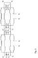
- an example power combiner structure is outlined in Figure 2 according to embodiments herein.
- the power combiner 200 in Figure 2 may be used to combine the outputs of two differential power amplifiers 210, 220 into a single-ended output. This is the same basic functionality as that of the combiner shown in Figure 1 . To perform this functionality, the power combiner 200 features three transformers 230, 240, 250. Transformers 230, 240 are coupled to power amplifiers 210, 220, respectively. Transformer 250 has balun function and is coupled to the load 260.
- FIG. 3 a schematic model 300 of the power combiner 200 is shown in Figure 3 .
- the schematic model 300 only shows the model of transformers 230, 240 without the balun 250 and load 260.
- the capacitors C1, C2, C3, C4 in Figure 3 are inter-winding capacitance between the primary and secondary windings of the transformers 230, 240 shown in Figure 2 .
- the coupling from V 1 + via capacitor C 1 + on the positive side is cancelled by coupling from V 1 - via capacitor C 1 - on the negative side to the primary winding of the transformer. Therefore the power combiner 200 has very nice property of leakage cancellation between the primary and secondary windings.
- the power combiner 200 in Figure 2 combines output power from the power amplifiers 210, 220 in a manner where the load balun 250 is placed beside the PA transformers 230, 240.
- the transformers 230, 240, 250 are connected in series and arranged along a line, here a horizontal line 270.
- the principle of this structure is that the voltage of the black trace, i.e. an inductor loop 201 formed by the windings of the transformer 230, 240, 250, is symmetric with respect to the horizontal line 270. That is a signal voltage at a point on the upper half, e.g. V 1 + , V 2 + , V 3 + , is accompanied by the opposite polarity signal voltage at the corresponding point on the lower half, e.g.
- Some non-symmetry may occur also in the structure of Figure 2 , but it may be made small enough not to affect the power amplifier performance. This may occur due to the common-mode voltage inevitably existing on the load side of the load balun 250. The situation may be helped by rotating the secondary winding of the balun 250 by 90 degrees. That is the output port of the transformer 250 may be directed upwards or downwards instead of to the side. Also combining output powers from the power amplifiers may be done with the load balun 250 placed in between the PA transformers.
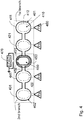
- Figure 4 shows such a combiner network 400 featuring combination of two branches of power amplifiers.
- each transformer branch comprises an inductor loop 401, 402.
- the inductor loop 401 comprises windings 411, 421, 451
- the inductor loop 402 comprises windings 431, 441, 452.
- the two transformer branches are connected in parallel in such a way that the last winding 451 of the inductor loop 401 of the first transformer branch is placed concentrically to the last winding 452 of the inductor loop 402 of the second transformer branch.
- Each transformer branch further comprises a number of primary inductors.
- Each primary inductor comprises a winding placed concentrically to one winding of the inductor loop.
- a winding 412 of a primary inductor in the first transformer branch is placed concentrically to the winding 411 of the inductor loop 401, thereby the winding 411 of the first inductor loop 401 and the primary inductor winding 412 form a transformer.
- Each primary inductor is coupled to a differential output of one of multiple differential power amplifiers.
- the primary inductor winding 412 is coupled to differential outputs of a differential power amplifier 460.
- the combiner network 400 further comprises a secondary inductor comprising a winding 453.
- the secondary inductor winding 453 is coupled to a single-ended load 470.
- a load balun or transformer 450 is thereby formed by placing the secondary inductor winding 453 concentrically to the two said last windings 451, 452 of the two inductor loops 401, 402.
- the “primary” side of the transformer is usually the side that takes power, e.g. the primary inductor winding 412 takes power from PA 460.
- the “secondary” is usually the side that delivers power, e.g. the secondary inductor winding 453 delivers power to the load.
- the winding 451 in the first inductor loop 401 may be considered as a primary inductor winding compared to the secondary inductor winding 453, as it takes power from both windings 411, 421 in the first transformer branch. The same may apply to the winding 452 in the second inductor loop 402.
- FIG. 5 shows another example of a combiner network 500 according to embodiments herein.
- two transformer branches are connected in series by a load balun 550. It may also be seen as two transformer branches merged to one transformer branch comprising a number of PA transformers and a centrally located balun 550.
- the load balun 550 shown in Figure 5 is placed in the middle of the transformer branch, it may be placed at any other place along the transformer branch.
- the transformer branch further comprises a number of primary inductors.
- Each primary inductor comprises a winding, e.g. winding 512, placed concentrically to one winding of the inductor loop 501, e.g. the winding 511.
- the number of primary inductors and the set of windings in the inductor loop 501 thereby form a number of transformers coupled to a number of differential amplifiers.
- the combiner network 500 further comprises a secondary inductor comprising a winding 552.
- the secondary inductor winding 552 is coupled to a single-ended load 570.
- a load balun or transformer 550 is thereby formed by placing the secondary inductor winding 552 concentrically to one winding, e.g. the winding 551, of the inductor loop 501.
- the combiner network 200, 400, 500 is easily scalable to a different number of power amplifiers per branch, and to a different number of transformer branches. That is an arbitrary number of transformers can be connected in series in a transformer branch, and more than one transformer branch may be combined with a very compact layout.
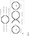
- Figure 6 shows an inductor loop 600 comprising a set of N windings which may be implemented in a transformer branch according to embodiments herein.
- Each winding comprises a first internal node, a second internal node, a third internal node, and a fourth internal node.
- Each winding has a first half winding connected between the first internal node and the third internal node, and a second half winding connected between the second internal node and the fourth internal node.
- the N set of windings is connected in the following ways:
- the set of N windings is interconnected and formed to an inductor loop.
- the inductor loop together with a number of primary inductors and one secondary inductor can constitute a number of transformers as discussed above with reference to Figure 4 and 5 .
- the power combiner network 200, 400, 500 and the inductor loop 600 may be implemented on a chip as an integrated transformer arrangement for combining output signals of multiple differential power amplifiers to a single-ended load.
- the integrated transformer arrangement comprises a first transformer branch.
- the first transformer branch comprises an inductor loop comprising a set of N ⁇ 3 windings.
- Each winding comprises a first internal node, a second internal node, a third internal node, and a fourth internal node.
- a first half winding connected between the first internal node and the third internal node, and a second half winding connected between the second internal node and the fourth internal node.
- the first internal node and the second internal node of the 1st winding are interconnected.
- the third internal node and the fourth internal node of the Nth winding are interconnected.
- the first internal node and the second internal node of the jth winding, 2 ⁇ j ⁇ N, are connected to the third internal node and the fourth internal node, respectively, of the (j-1)th winding.
- the first transformer branch further comprises a number of primary inductors, wherein each primary inductor comprises a winding placed concentrically to one winding of the inductor loop, and each primary inductor is configured to couple to a differential output of one of the multiple differential power amplifiers.
- the integrated transformer arrangement further comprises a secondary inductor comprising a winding placed concentrically to a winding of the inductor loop, and the secondary inductor is configured to couple to the single-ended load.
- the inductor loop and the number of primary inductors in the first transformer branch form a number of series connected transformers to combine output signals from a number of the differential power amplifiers;
- the secondary inductor together with a winding of the inductor loop form a balun transformer that transforms a balanced signal to an unbalanced signal.
- the integrated transformer arrangement may comprise a second transformer branch coupled in parallel with the first transformer branch.
- the M windings are arranged and connected in a similar way as the N windings of the inductor loop in the first transformer branch.
- M may be the same as N or not.
- the M windings and the number of primary inductors in the second transformer branch may be arranged in a similar structure as the first transformer branch.
- the Nth winding of the inductor loop of the first transformer branch is placed concentrically to the Mth winding of the inductor loop of the second transformer branch, and wherein the winding of the secondary inductor coupled to the single-ended load is placed concentrically to the said Nth and Mth windings.
- the windings of the inductor loop 201, 401, 501, 600, and the windings of the primary and secondary inductors comprise only one turn, according to some embodiments herein the windings of any inductors may comprise one or more turns.
- the number of transformers is arranged along a horizontal line, they may be arranged along a vertical line, or along a line in any direction. Further the line may not necessarily be a straight line along all transformers, any other type of lines, e.g. a curved line, a staircase line, will work as well as long as the first half winding of each winding in the inductor loop is symmetrical to its second half winding about the line.
- placed concentrically to is to describe the psychical relationship or relative position between two windings in a transformer.
- the power combiner network 200, 400, 500 is implemented on a chip as an integrated transformer arrangement, two windings placed concentrically to each other may be implemented in different ways. If the same metal layer is used for both primary and second windings, one winding may be placed inside or outside the other winding. If different metal layers are used for two windings, one winding may be placed above or below the other winding.
- Figure 7 shows voltages at PA outputs versus frequency for the prior art power combiner shown in Figure 1 and the proposed solution shown in Figure 2 .
- the curve 701 in the middle shows the simulation result of the positive and negative output voltages of one power amplifier, e.g. PA 220 in the power combiner network or integrated transformer arrangement 200 shown in Figure 2 , where no voltage difference between the plus and minus terminal of the PA outputs is noticed. Therefore, impedance at the outputs of any one of the power amplifiers PA 220, 210 is balanced.
- the voltages at the plus and minus terminals of the PA outputs differ by about 63% at 20GHz, shown by curves 702 and 703, which means impedance imbalance occurs at the outputs of any one of the two power amplifiers.
- the voltages shown in Figure 7 varies with frequency since the impedances of the combiner, both in prior art and the proposed solution, are frequency dependent.
- a number of series connected transformers formed by an inductor loop and a number of primary inductors are used to combine output signals from a number of the differential power amplifiers.
- a balun transformer formed by a secondary inductor together with a winding of the inductor loop is used to transform a balanced signal to an unbalanced signal. In this way, symmetrical impedance is achieved when combining output signals from the differential power amplifiers.
- An arbitrary number of transformers can be connected in series in a branch, which is enabled by windings in the inductor loop that have input/output ports on two sides.
- the primary inductors coupled to the power amplifiers may be rotated, e.g.
- More than one transformer branch may be combined, for instance, using a load transformer or balun with a winding that used as both balun and combiner. In this way, two or more branches may be used with a very compact layout.
- FIG. 8 shows a block diagram for an electronic device 800.
- the electronic device 800 comprises a power amplifier PA 810, in which the integrated transformer arrangement 200, 400, 500 may be implemented.
- the electronic device 800 may be a user equipment or a mobile device, a base station or multi-antenna systems in a radio base station, a transmitter, a transceiver etc. in a cellular communications network.
- the electronic device 800 may comprise other units, where a processing unit 830 is shown.
- the integrated transformer arrangement 200, 400, 500 may be implemented by any semiconductor technology, e.g. Metal-Oxide-Semiconductor, CMOS or Micro-Electro-Mechanical Systems (MEMS) technology etc.
- semiconductor technology e.g. Metal-Oxide-Semiconductor, CMOS or Micro-Electro-Mechanical Systems (MEMS) technology etc.
Landscapes
- Engineering & Computer Science (AREA)
- Power Engineering (AREA)
- Multimedia (AREA)
- Microelectronics & Electronic Packaging (AREA)
- Amplifiers (AREA)
Description
- Embodiments herein relate to an integrated transformer arrangement. In particular, they relate to an integrated transformer arrangement for combining output signals of multiple differential amplifiers to a single-ended load, and a power amplifier and an electronic device comprising the integrated transformer arrangement.
- In modern wireless communication systems, due to a shortage of available spectrum at lower frequencies there is a strong interest in using millimeter or micro waves with high frequencies for high data-rate communication. The use of millimeter waves will thus be an important part of upcoming 5th generation (5G) cellular systems. However, some major challenges must be solved. One of the most important ones is how to achieve sufficient transmit output power at high frequencies using low cost semiconductor technologies, such as Complementary Metal Oxide Semiconductor (CMOS). Although the speed of CMOS devices in the latest technologies is sufficient for implementing millimeter wave amplifiers, the supply voltage is severely limited. It is therefore difficult to obtain high output power. This is addressed by power combination, where outputs of a number of smaller amplifiers are combined to a single output signal. In this way substantially higher output power can be achieved compared to that of a single power amplifier.
- A key part of a high performance millimeter wave power amplifier in low cost technology is combining network. A combining network should be able to both combine output powers or signals of several power amplifiers with very low loss and show same impedance to all incoming signals. If the impedance of the combining network seen by the power amplifiers is different, the power amplifiers will not be able to deliver the same output power. Then some of the power amplifiers will be subjected to higher voltages than others, which will cause reliability concerns. In addition, distortion generation will also increase. A key problem in the combination network is that balun functionality is needed. This is due to that power amplifiers integrated on a chip are preferably in differential structure and output differential signals, while a single-ended signal to an antenna is typically desired. The balun functionality unfortunately makes it difficult to obtain impedance balance. While combination networks based on transformers have been demonstrated with low loss and balun functionality, the important property of impedance balance is still missing.
Figure 1 shows such a combination network, presented in A. Tuffery, et. al, "CMOS fully integrated reconfigurable power amplifier with efficiency enhancement for LTE applications", Electronics Letters, Vol. 51, . As shown inFigure 1 , the combination network has twoidentical transformers load balun 130 connected in between. V2 is a symmetry point, resulting in significant common-mode signal voltage in the PA transformer secondary windings. The capacitors shown inFigure 1 are parasitic capacitors between the primary and secondary windings, i.e. inter-winding parasitic capacitance. When a common-mode signal voltage is present, an impedance imbalance may occur due to the inter-winding parasitic capacitance. -
ES 2206053 A1 -
US 2014/084700 A1 discloses an RF front end module circuit that provides high linearity and power efficiency and meets the requirements of modern wireless communication standards. The front end module circuit includes a power amplifier made up of one or more sub-amplifiers having high and low power circuits and whose outputs are combined to yield the total desired power gain. An integrated multi-tap transformer having primary and secondary windings provide power combining and transfer to the antenna of the power generated by the individual sub-amplifiers. - ERCAN KAYMAKSUT ET AL: "Analysis and Optimization of Transformer-Based Power Combining for Back-Off Efficiency Enhancement", IEEE TRANSACTIONS ON CIRCUITS AND SYSTEMS I: REGULAR PAPERS, IEEE, US, vol. 60, no. 4, 1 April 2013 (2013-04-01), pages 825-835, analyzes the back-off efficiency enhancement characteristics of transformer combined power amplifiers taking into account the amplifier and transformer parasitics. The dynamic power combining properties of different transformer architectures are investigated. The co-optimization of the transformer and the amplifiers is presented for the transformer-based Doherty power amplifier which is a linear class of operation with back-off efficiency enhancement. Then this analysis is extended for the uneven Doherty power amplifier which employs asymmetrical transformers. The proposed design methodology is used to design a 2.4 GHz uneven Doherty power amplifier in standard 90 nm CMOS technology.
- Therefor it is an object of embodiments herein to provide an integrated combining network with improved performance for combining output signals of multiple differential power amplifiers.
- According to the present invention, the object is achieved by an integrated transformer arrangement for combining output signals of multiple differential amplifiers to a single-ended load. The integrated transformer arrangement comprises a first transformer branch. The first transformer branch comprises an inductor loop comprising a set of N≥3 windings. Each winding comprises a first internal node, a second internal node, a third internal node, and a fourth internal node. Each winding further comprises a first half winding connected between the first internal node and the third internal node; a second half winding connected between the second internal node and the fourth internal node. Further, the N set of windings are connected in such a way that the first internal node and the second internal node of the 1st winding are interconnected, the third internal node and the fourth internal node of the Nth winding are interconnected, and the first internal node and the second internal node of the jth winding, 2≤j≤N, are connected to the third internal node and the fourth internal node, respectively, of the (j-1)th winding.
- The first transformer branch further comprises a number of primary inductors. Each primary inductor comprises a winding placed concentrically to one winding of the inductor loop, and each primary inductor is configured to couple to a differential output of one of the multiple differential amplifiers.
- The integrated transformer arrangement further comprises a secondary inductor comprising a winding placed concentrically to a winding of the inductor loop, and the secondary inductor is configured to couple to the single-ended load.
- In other words, according to some embodiments herein, the inductor loop and the number of primary inductors in the first transformer branch form a number of series connected transformers to combine output signals from a number of the differential power amplifiers; the secondary inductor together with a winding of the inductor loop form a balun transformer that transforms a balanced signal to an unbalanced signal. In this way, a symmetrical impedance is achieved when combining output signals from the differential power amplifiers. This is due to that the number of series connected transformers may be arranged along a line, either horizontal or vertical, such that the first half winding of each winding in the inductor loop is symmetrical to its second half winding about the line. In this way, it is ensured that voltage of the inductor loop is symmetric with respect to the symmetry line. That is, for each winding of the inductor loop, a signal voltage at a point on the first half winding is accompanied by an opposite signal voltage at a corresponding point on the second half winding. Summing the voltage of any winding of the inductor loop, the result is then zero, as a voltage at one half winding on the one side of the line is cancelled by the opposite voltage on the other half winding. The common mode voltage is then zero or close to zero, resulting in no or close to no difference in impedance between the differential PA inputs. When a common-mode signal voltage is present, an impedance imbalance occurs due to the inter-winding capacitance between the winding of the primary inductors and the winding of the inductor loop.
- The integrated transformer arrangement is scalable to a different number of power amplifiers per branch, and to a different number of branches. That is an arbitrary number of transformers can be connected in series in a transformer branch, and more than one branch may be combined with a very compact layout.
- Therefore, the integrated transformer arrangement according to embodiments herein provides a combiner network with low loss which converts the differential outputs of the power amplifiers to a single-ended load.
- Examples of embodiments herein are described in more detail with reference to attached drawings in which:
- Figure 1
- is a schematic view of a combination network according to prior art;
- Figure 2
- is a schematic view of a combiner network according to embodiments herein;
- Figure 3
- is a schematic view illustrating a circuit model of the combiner network in
Figure 2 ; - Figure 4
- is a schematic view illustrating a combiner network according to embodiments herein;
- Figure 5
- is a schematic view illustrating a combiner network according to embodiments herein;
- Figure 6
- is a schematic view illustrating an inductor loop according to embodiments herein;
- Figure 7
- is a diagram illustrating simulation results;
- Figure 8
- is a block diagram illustrating an electronic device in which embodiments herein may be implemented.
- To achieve a power combiner with low loss and balun functionality, where all input terminals have the same impedance, an example power combiner structure is outlined in
Figure 2 according to embodiments herein. - The power combiner 200 in
Figure 2 may be used to combine the outputs of twodifferential power amplifiers Figure 1 . To perform this functionality, the power combiner 200 features threetransformers Transformers power amplifiers Transformer 250 has balun function and is coupled to theload 260. - To analyze and illustrate functionality and advantage of the power combiner 200 in
Figure 2 , a schematic model 300 of the power combiner 200 is shown inFigure 3 . The schematic model 300 only shows the model oftransformers balun 250 andload 260. The capacitors C1, C2, C3, C4 inFigure 3 are inter-winding capacitance between the primary and secondary windings of thetransformers Figure 2 . Here it is clearly seen that the coupling from V1 + via capacitor C1 +on the positive side is cancelled by coupling from V1 - via capacitor C1 - on the negative side to the primary winding of the transformer. Therefore the power combiner 200 has very nice property of leakage cancellation between the primary and secondary windings. - The power combiner 200 in
Figure 2 combines output power from thepower amplifiers load balun 250 is placed beside thePA transformers transformers horizontal line 270. The principle of this structure is that the voltage of the black trace, i.e. aninductor loop 201 formed by the windings of thetransformer horizontal line 270. That is a signal voltage at a point on the upper half, e.g. V1 +, V2 +, V3 +, is accompanied by the opposite polarity signal voltage at the corresponding point on the lower half, e.g. V1 -, V2 -, V3 -. Summing the voltage of one winding of theinductor loop 201, the result is then zero, as a voltage at the top half is always cancelled by the opposite voltage on the bottom half. The common mode voltage is then zero, resulting in no difference in impedance between the differential PAs inputs Vo +, Vo -. When a common-mode signal voltage is present, an impedance imbalance occurs due to the inter-winding capacitance. This happens in the structure ofFigure 1 , where V2 is a symmetry point, resulting in significant common-mode signal voltage in the PA transformer secondary windings. - Some non-symmetry may occur also in the structure of
Figure 2 , but it may be made small enough not to affect the power amplifier performance. This may occur due to the common-mode voltage inevitably existing on the load side of theload balun 250. The situation may be helped by rotating the secondary winding of thebalun 250 by 90 degrees. That is the output port of thetransformer 250 may be directed upwards or downwards instead of to the side. Also combining output powers from the power amplifiers may be done with theload balun 250 placed in between the PA transformers. -
Figure 4 shows such acombiner network 400 featuring combination of two branches of power amplifiers. - In
Figure 4 , there are two PA transformer branches connected in parallel. Each transformer branch comprises aninductor loop inductor loop inductor loop 401 compriseswindings inductor loop 402 compriseswindings inductor loop 401 of the first transformer branch is placed concentrically to the last winding 452 of theinductor loop 402 of the second transformer branch. - Each transformer branch further comprises a number of primary inductors. Each primary inductor comprises a winding placed concentrically to one winding of the inductor loop. For example, a winding 412 of a primary inductor in the first transformer branch is placed concentrically to the winding 411 of the
inductor loop 401, thereby the winding 411 of thefirst inductor loop 401 and the primary inductor winding 412 form a transformer. Each primary inductor is coupled to a differential output of one of multiple differential power amplifiers. For example, the primary inductor winding 412 is coupled to differential outputs of adifferential power amplifier 460. - The
combiner network 400 further comprises a secondary inductor comprising a winding 453. The secondary inductor winding 453 is coupled to a single-endedload 470. A load balun ortransformer 450 is thereby formed by placing the secondary inductor winding 453 concentrically to the two saidlast windings inductor loops - Here terminology such as "primary inductor" and "secondary inductor" are used to differentiate the two windings in a transformer and should not be considered to limit the scope of the embodiments herein. The "primary" side of the transformer is usually the side that takes power, e.g. the primary inductor winding 412 takes power from
PA 460. The "secondary" is usually the side that delivers power, e.g. the secondary inductor winding 453 delivers power to the load. The winding 451 in thefirst inductor loop 401 may be considered as a primary inductor winding compared to the secondary inductor winding 453, as it takes power from bothwindings second inductor loop 402. -
Figure 5 shows another example of acombiner network 500 according to embodiments herein. InFigure 5 , two transformer branches are connected in series by aload balun 550. It may also be seen as two transformer branches merged to one transformer branch comprising a number of PA transformers and a centrally locatedbalun 550. Although theload balun 550 shown inFigure 5 is placed in the middle of the transformer branch, it may be placed at any other place along the transformer branch. - The transformer branch comprises an
inductor loop 501 comprising a set of N windings 511-551, i.e. N=5. - The transformer branch further comprises a number of primary inductors. Each primary inductor comprises a winding, e.g. winding 512, placed concentrically to one winding of the
inductor loop 501, e.g. the winding 511. The number of primary inductors and the set of windings in theinductor loop 501 thereby form a number of transformers coupled to a number of differential amplifiers. - The
combiner network 500 further comprises a secondary inductor comprising a winding 552. The secondary inductor winding 552 is coupled to a single-endedload 570. A load balun ortransformer 550 is thereby formed by placing the secondary inductor winding 552 concentrically to one winding, e.g. the winding 551, of theinductor loop 501. - The
combiner network -
Figure 6 shows aninductor loop 600 comprising a set of N windings which may be implemented in a transformer branch according to embodiments herein. - Each winding comprises a first internal node, a second internal node, a third internal node, and a fourth internal node.
- Each winding has a first half winding connected between the first internal node and the third internal node, and a second half winding connected between the second internal node and the fourth internal node.
- The N set of windings is connected in the following ways:
- the first internal node and the second internal node of the 1st winding are interconnected;
- the third internal node and the fourth internal node of the Nth winding are interconnected;
- the first internal node and the second internal node of the jth winding, 2 ≤ j ≤ N, are connected to the third internal node and the fourth internal node, respectively, of the (j - 1)th winding. This can be seen as that the 2nd winding to the (N-1)th winding in the middle of the inductor loop have input/output ports on two sides, as shown on top of
Figure 6 , which enable all windings to be connected in series. - In this way, the set of N windings is interconnected and formed to an inductor loop. The inductor loop together with a number of primary inductors and one secondary inductor can constitute a number of transformers as discussed above with reference to
Figure 4 and5 . - The
power combiner network inductor loop 600 may be implemented on a chip as an integrated transformer arrangement for combining output signals of multiple differential power amplifiers to a single-ended load. - Therefore, according to embodiments herein, the integrated transformer arrangement comprises a first transformer branch.
- The first transformer branch comprises an inductor loop comprising a set of N≥3 windings.
- Each winding comprises a first internal node, a second internal node, a third internal node, and a fourth internal node. A first half winding connected between the first internal node and the third internal node, and a second half winding connected between the second internal node and the fourth internal node.
- The first internal node and the second internal node of the 1st winding are interconnected. The third internal node and the fourth internal node of the Nth winding are interconnected.
- The first internal node and the second internal node of the jth winding, 2≤j≤N, are connected to the third internal node and the fourth internal node, respectively, of the (j-1)th winding.
- The first transformer branch further comprises a number of primary inductors, wherein each primary inductor comprises a winding placed concentrically to one winding of the inductor loop, and each primary inductor is configured to couple to a differential output of one of the multiple differential power amplifiers.
- The integrated transformer arrangement further comprises a secondary inductor comprising a winding placed concentrically to a winding of the inductor loop, and the secondary inductor is configured to couple to the single-ended load.
- With the structure of the integrated transformer arrangement as described above, the inductor loop and the number of primary inductors in the first transformer branch form a number of series connected transformers to combine output signals from a number of the differential power amplifiers; the secondary inductor together with a winding of the inductor loop form a balun transformer that transforms a balanced signal to an unbalanced signal.
- According to some embodiments herein, the integrated transformer arrangement may comprise a second transformer branch coupled in parallel with the first transformer branch. The second transformer branch comprises an inductor loop comprising a set of M windings and a number of primary inductors, where M=3, 4.... The M windings are arranged and connected in a similar way as the N windings of the inductor loop in the first transformer branch. M may be the same as N or not. The M windings and the number of primary inductors in the second transformer branch may be arranged in a similar structure as the first transformer branch. The Nth winding of the inductor loop of the first transformer branch is placed concentrically to the Mth winding of the inductor loop of the second transformer branch, and wherein the winding of the secondary inductor coupled to the single-ended load is placed concentrically to the said Nth and Mth windings. The
combiner network 400 discussed above with reference toFigure 4 is a specific example of an integrated transformer arrangement comprising two transformer branches coupled in parallel, where N=M=3. - Although shown in
Figures 2 ,4 ,5 and6 , the windings of theinductor loop - As shown in
Figures 2 ,4 ,5 and6 , although the number of transformers is arranged along a horizontal line, they may be arranged along a vertical line, or along a line in any direction. Further the line may not necessarily be a straight line along all transformers, any other type of lines, e.g. a curved line, a staircase line, will work as well as long as the first half winding of each winding in the inductor loop is symmetrical to its second half winding about the line. - The terminology "placed concentrically to" used above is to describe the psychical relationship or relative position between two windings in a transformer. When the
power combiner network - In order to show the performance of the power combiner network or
integrated transformer arrangement -
Figure 7 shows voltages at PA outputs versus frequency for the prior art power combiner shown inFigure 1 and the proposed solution shown inFigure 2 . The curve 701 in the middle shows the simulation result of the positive and negative output voltages of one power amplifier,e.g. PA 220 in the power combiner network or integrated transformer arrangement 200 shown inFigure 2 , where no voltage difference between the plus and minus terminal of the PA outputs is noticed. Therefore, impedance at the outputs of any one of thepower amplifiers PA Figure 1 , the voltages at the plus and minus terminals of the PA outputs differ by about 63% at 20GHz, shown bycurves Figure 7 varies with frequency since the impedances of the combiner, both in prior art and the proposed solution, are frequency dependent. - To summarize, in the
integrated transformer arrangement - The
integrated transformer arrangement Figure 8 shows a block diagram for anelectronic device 800. Theelectronic device 800 comprises apower amplifier PA 810, in which theintegrated transformer arrangement electronic device 800 may be a user equipment or a mobile device, a base station or multi-antenna systems in a radio base station, a transmitter, a transceiver etc. in a cellular communications network. Theelectronic device 800 may comprise other units, where aprocessing unit 830 is shown. - Those skilled in the art will understand that the
integrated transformer arrangement - When using the word "comprise" or "comprising" it shall be interpreted as non- limiting, i.e. meaning "consist at least of".
- The embodiments herein are not limited to the above described preferred embodiments. Various alternatives, modifications and equivalents may be used. Therefore, the above embodiments should not be taken as limiting the scope of the invention, which is defined by the appended claims.
Claims (7)
- An integrated transformer arrangement (200, 400, 500) for combining output signals of multiple differential amplifiers to a single-ended load, wherein the integrated transformer arrangement comprises:a first transformer branch, wherein the first transformer branch comprises:
an inductor loop (401, 501) comprising a set of N≥3 windings, wherein each winding comprises:- a first internal node, a second internal node, a third internal node, and a fourth internal node;- a first half winding connected between the first internal node and the third internal node;- a second half winding connected between the second internal node and the fourth internal node; and wherein,- the first internal node and the second internal node of the 1st winding (411, 511, 601) are interconnected;- the third internal node and the fourth internal node of the Nth winding (451, 541, 60N) are interconnected;- the first internal node and the second internal node of the jth winding (421, 521, 531), 2≤j≤N, are connected to the third internal node and the fourth internal node, respectively, of the (j-1)th winding; andthe first transformer branch further comprises:a number of primary inductors, wherein each primary inductor comprises a winding (412, 512) placed concentrically to one winding of the inductor loop, and each primary inductor is configured to couple to a differential output of one of the multiple differential amplifiers; and
the integrated transformer arrangement further comprises:
a secondary inductor comprising a winding (453, 552) placed concentrically to a winding of the inductor loop, and the secondary inductor is configured to couple to the single-ended load. - The integrated transformer arrangement (200, 400, 500) according to claim 1 further comprising a second transformer branch coupled in parallel with the first transformer branch, wherein the second transformer branch comprises an inductor loop (402) comprising a set of M windings connected in series, M≥3, and a number of primary inductors arranged in a similar structure as the first transformer branch.
- The integrated transformer arrangement (200, 400, 500) according to claim 2, wherein the Nth winding of the inductor loop of the first transformer branch is placed concentrically to the Mth winding of the inductor loop of the second transformer branch, and wherein the winding of the secondary inductor coupled to the single-ended load is placed concentrically to the said Nth and Mth windings.
- The integrated transformer arrangement (200, 400, 500) according to any one of claims 1-3, wherein the winding of any inductor comprises one or more turns.
- A power amplifier (810) comprising an integrated transformer arrangement (200, 400, 500) according to any one of claims 1-4.
- An electronic device (800) comprising an integrated transformer arrangement (200, 400, 500) according to any one of claims 1-4.
- The electronic device (800) according to claim 6 is any one of a user equipment, a mobile device, a base station or multi-antenna systems in a radio base station, a transmitter, a transceiver in a cellar communications network.
Applications Claiming Priority (1)
| Application Number | Priority Date | Filing Date | Title |
|---|---|---|---|
| PCT/EP2017/058532 WO2018188719A1 (en) | 2017-04-10 | 2017-04-10 | An integrated transformer |
Publications (2)
| Publication Number | Publication Date |
|---|---|
| EP3610489A1 EP3610489A1 (en) | 2020-02-19 |
| EP3610489B1 true EP3610489B1 (en) | 2021-01-27 |
Family
ID=58530551
Family Applications (1)
| Application Number | Title | Priority Date | Filing Date |
|---|---|---|---|
| EP17716531.3A Active EP3610489B1 (en) | 2017-04-10 | 2017-04-10 | An integrated transformer |
Country Status (5)
| Country | Link |
|---|---|
| US (1) | US11335493B2 (en) |
| EP (1) | EP3610489B1 (en) |
| KR (1) | KR102209324B1 (en) |
| CN (1) | CN110494939B (en) |
| WO (1) | WO2018188719A1 (en) |
Families Citing this family (2)
| Publication number | Priority date | Publication date | Assignee | Title |
|---|---|---|---|---|
| KR102934384B1 (en) * | 2023-07-27 | 2026-03-06 | 충남대학교산학협력단 | Power amplifier and drive amplifier |
| CN119543851B (en) * | 2023-08-30 | 2026-03-27 | 锐石创芯(深圳)半导体有限公司 | RF power amplifier and RF front-end module |
Family Cites Families (7)
| Publication number | Priority date | Publication date | Assignee | Title |
|---|---|---|---|---|
| ES2206053A1 (en) | 2002-10-24 | 2004-05-01 | Diseño De Sistemas En Silicio, S.A. | POWER COMBINER. |
| US7432794B2 (en) * | 2004-08-16 | 2008-10-07 | Telefonaktiebolaget L M Ericsson (Publ) | Variable integrated inductor |
| WO2009144211A1 (en) | 2008-05-29 | 2009-12-03 | Nxp B.V. | Radio frequency eight-shaped balun |
| KR101064659B1 (en) * | 2009-08-05 | 2011-09-15 | 전자부품연구원 | Multi-finger Transformers and Power Amplifiers Using the Same |
| KR101119279B1 (en) * | 2010-03-04 | 2012-03-20 | 삼성전기주식회사 | Power Amplifier |
| US9312820B2 (en) * | 2012-09-23 | 2016-04-12 | Dsp Group Ltd. | CMOS based TX/RX switch |
| US9705414B2 (en) | 2014-12-18 | 2017-07-11 | Infineon Technologies Austria Ag | System and method for zero voltage switching in continuous conductance mode (CCM) flyback converters |
-
2017
- 2017-04-10 CN CN201780089486.2A patent/CN110494939B/en active Active
- 2017-04-10 EP EP17716531.3A patent/EP3610489B1/en active Active
- 2017-04-10 KR KR1020197031445A patent/KR102209324B1/en active Active
- 2017-04-10 US US16/500,117 patent/US11335493B2/en active Active
- 2017-04-10 WO PCT/EP2017/058532 patent/WO2018188719A1/en not_active Ceased
Non-Patent Citations (1)
| Title |
|---|
| None * |
Also Published As
| Publication number | Publication date |
|---|---|
| US11335493B2 (en) | 2022-05-17 |
| KR20190127923A (en) | 2019-11-13 |
| WO2018188719A1 (en) | 2018-10-18 |
| US20210104349A1 (en) | 2021-04-08 |
| CN110494939A (en) | 2019-11-22 |
| EP3610489A1 (en) | 2020-02-19 |
| CN110494939B (en) | 2021-07-30 |
| KR102209324B1 (en) | 2021-01-28 |
Similar Documents
| Publication | Publication Date | Title |
|---|---|---|
| US8791769B2 (en) | Figure 8 balun | |
| Zhao et al. | A 40-nm CMOS E-band 4-way power amplifier with neutralized bootstrapped cascode amplifier and optimum passive circuits | |
| US20210135631A1 (en) | Wideband power combiner and splitter | |
| CN102868419B (en) | Transceiver and integrated circuit | |
| CN103368601B (en) | Wireless communication transceiver front end | |
| EP2736168A1 (en) | Class AB amplifiers | |
| US8314658B2 (en) | Power amplifier | |
| US20140306780A1 (en) | Duplexers | |
| CN106778413A (en) | A kind of integrated simulation self-interference cancellation circuit for being applied to ultrahigh frequency RFID | |
| CN103281040A (en) | On-chip power amplifier synthesized based on power of eight branches of fully symmetrical transformers | |
| Xue et al. | Two W-band wideband CMOS mmW PAs for automotive radar transceivers | |
| CN110391787B (en) | Power synthesizer and power amplifier integrated circuit | |
| Kim et al. | A 97–107 GHz Triple-Stacked-FET Power Amplifier with 23.7 dB Peak Gain, 15.1 dBm P SAT, and 18.6% PAE MAX in 28-nm FD-SOI CMOS | |
| CN111641391A (en) | Differential quadrature output low noise amplifier | |
| Wang et al. | A 26.5–29.5 GHz Doherty PA-LNA implementation with synthesized transformer-based matching network | |
| US8779826B1 (en) | Power splitter and combiner | |
| CN101951232A (en) | Radio-frequency (RF) power amplifier | |
| US11335493B2 (en) | Integrated transformer | |
| US9319007B2 (en) | Three-dimensional power amplifier architecture | |
| Chen et al. | A compact fully integrated high-efficiency 5GHz stacked class-E PA in 65nm CMOS based on transformer-based charging acceleration | |
| Chen et al. | A V-band inverse class F power amplifier with 16.3% PAE in 65nm CMOS | |
| CN101685704B (en) | Transformer and its structure and power amplifier | |
| KR20240020150A (en) | Output matching network with improved broadband characteristics and power amplifier network including the same | |
| Hassan et al. | A Compact 28-GHz Power Amplifier Design with a High Turn-Ratio Transformer for Enhanced $ P_ {{sat}} $ Without Power Combining in 22nm FDSOI CMOS | |
| Chen et al. | A 94-GHz Power Amplifier with Transformer-based Two-way Power Combining in 65-nm CMOS |
Legal Events
| Date | Code | Title | Description |
|---|---|---|---|
| STAA | Information on the status of an ep patent application or granted ep patent |
Free format text: STATUS: UNKNOWN |
|
| STAA | Information on the status of an ep patent application or granted ep patent |
Free format text: STATUS: THE INTERNATIONAL PUBLICATION HAS BEEN MADE |
|
| PUAI | Public reference made under article 153(3) epc to a published international application that has entered the european phase |
Free format text: ORIGINAL CODE: 0009012 |
|
| STAA | Information on the status of an ep patent application or granted ep patent |
Free format text: STATUS: REQUEST FOR EXAMINATION WAS MADE |
|
| 17P | Request for examination filed |
Effective date: 20191014 |
|
| AK | Designated contracting states |
Kind code of ref document: A1 Designated state(s): AL AT BE BG CH CY CZ DE DK EE ES FI FR GB GR HR HU IE IS IT LI LT LU LV MC MK MT NL NO PL PT RO RS SE SI SK SM TR |
|
| AX | Request for extension of the european patent |
Extension state: BA ME |
|
| DAV | Request for validation of the european patent (deleted) | ||
| DAX | Request for extension of the european patent (deleted) | ||
| GRAP | Despatch of communication of intention to grant a patent |
Free format text: ORIGINAL CODE: EPIDOSNIGR1 |
|
| STAA | Information on the status of an ep patent application or granted ep patent |
Free format text: STATUS: GRANT OF PATENT IS INTENDED |
|
| INTG | Intention to grant announced |
Effective date: 20200929 |
|
| GRAS | Grant fee paid |
Free format text: ORIGINAL CODE: EPIDOSNIGR3 |
|
| GRAA | (expected) grant |
Free format text: ORIGINAL CODE: 0009210 |
|
| STAA | Information on the status of an ep patent application or granted ep patent |
Free format text: STATUS: THE PATENT HAS BEEN GRANTED |
|
| AK | Designated contracting states |
Kind code of ref document: B1 Designated state(s): AL AT BE BG CH CY CZ DE DK EE ES FI FR GB GR HR HU IE IS IT LI LT LU LV MC MK MT NL NO PL PT RO RS SE SI SK SM TR |
|
| REG | Reference to a national code |
Ref country code: GB Ref legal event code: FG4D |
|
| REG | Reference to a national code |
Ref country code: CH Ref legal event code: EP |
|
| REG | Reference to a national code |
Ref country code: AT Ref legal event code: REF Ref document number: 1359098 Country of ref document: AT Kind code of ref document: T Effective date: 20210215 |
|
| REG | Reference to a national code |
Ref country code: IE Ref legal event code: FG4D |
|
| REG | Reference to a national code |
Ref country code: DE Ref legal event code: R096 Ref document number: 602017032044 Country of ref document: DE |
|
| REG | Reference to a national code |
Ref country code: NL Ref legal event code: FP |
|
| REG | Reference to a national code |
Ref country code: LT Ref legal event code: MG9D |
|
| REG | Reference to a national code |
Ref country code: AT Ref legal event code: MK05 Ref document number: 1359098 Country of ref document: AT Kind code of ref document: T Effective date: 20210127 |
|
| PG25 | Lapsed in a contracting state [announced via postgrant information from national office to epo] |
Ref country code: NO Free format text: LAPSE BECAUSE OF FAILURE TO SUBMIT A TRANSLATION OF THE DESCRIPTION OR TO PAY THE FEE WITHIN THE PRESCRIBED TIME-LIMIT Effective date: 20210427 Ref country code: PT Free format text: LAPSE BECAUSE OF FAILURE TO SUBMIT A TRANSLATION OF THE DESCRIPTION OR TO PAY THE FEE WITHIN THE PRESCRIBED TIME-LIMIT Effective date: 20210527 Ref country code: HR Free format text: LAPSE BECAUSE OF FAILURE TO SUBMIT A TRANSLATION OF THE DESCRIPTION OR TO PAY THE FEE WITHIN THE PRESCRIBED TIME-LIMIT Effective date: 20210127 Ref country code: FI Free format text: LAPSE BECAUSE OF FAILURE TO SUBMIT A TRANSLATION OF THE DESCRIPTION OR TO PAY THE FEE WITHIN THE PRESCRIBED TIME-LIMIT Effective date: 20210127 Ref country code: GR Free format text: LAPSE BECAUSE OF FAILURE TO SUBMIT A TRANSLATION OF THE DESCRIPTION OR TO PAY THE FEE WITHIN THE PRESCRIBED TIME-LIMIT Effective date: 20210428 Ref country code: BG Free format text: LAPSE BECAUSE OF FAILURE TO SUBMIT A TRANSLATION OF THE DESCRIPTION OR TO PAY THE FEE WITHIN THE PRESCRIBED TIME-LIMIT Effective date: 20210427 Ref country code: LT Free format text: LAPSE BECAUSE OF FAILURE TO SUBMIT A TRANSLATION OF THE DESCRIPTION OR TO PAY THE FEE WITHIN THE PRESCRIBED TIME-LIMIT Effective date: 20210127 |
|
| PG25 | Lapsed in a contracting state [announced via postgrant information from national office to epo] |
Ref country code: SE Free format text: LAPSE BECAUSE OF FAILURE TO SUBMIT A TRANSLATION OF THE DESCRIPTION OR TO PAY THE FEE WITHIN THE PRESCRIBED TIME-LIMIT Effective date: 20210127 Ref country code: AT Free format text: LAPSE BECAUSE OF FAILURE TO SUBMIT A TRANSLATION OF THE DESCRIPTION OR TO PAY THE FEE WITHIN THE PRESCRIBED TIME-LIMIT Effective date: 20210127 Ref country code: RS Free format text: LAPSE BECAUSE OF FAILURE TO SUBMIT A TRANSLATION OF THE DESCRIPTION OR TO PAY THE FEE WITHIN THE PRESCRIBED TIME-LIMIT Effective date: 20210127 Ref country code: PL Free format text: LAPSE BECAUSE OF FAILURE TO SUBMIT A TRANSLATION OF THE DESCRIPTION OR TO PAY THE FEE WITHIN THE PRESCRIBED TIME-LIMIT Effective date: 20210127 Ref country code: LV Free format text: LAPSE BECAUSE OF FAILURE TO SUBMIT A TRANSLATION OF THE DESCRIPTION OR TO PAY THE FEE WITHIN THE PRESCRIBED TIME-LIMIT Effective date: 20210127 |
|
| PG25 | Lapsed in a contracting state [announced via postgrant information from national office to epo] |
Ref country code: IS Free format text: LAPSE BECAUSE OF FAILURE TO SUBMIT A TRANSLATION OF THE DESCRIPTION OR TO PAY THE FEE WITHIN THE PRESCRIBED TIME-LIMIT Effective date: 20210527 |
|
| REG | Reference to a national code |
Ref country code: DE Ref legal event code: R097 Ref document number: 602017032044 Country of ref document: DE |
|
| PG25 | Lapsed in a contracting state [announced via postgrant information from national office to epo] |
Ref country code: SM Free format text: LAPSE BECAUSE OF FAILURE TO SUBMIT A TRANSLATION OF THE DESCRIPTION OR TO PAY THE FEE WITHIN THE PRESCRIBED TIME-LIMIT Effective date: 20210127 Ref country code: EE Free format text: LAPSE BECAUSE OF FAILURE TO SUBMIT A TRANSLATION OF THE DESCRIPTION OR TO PAY THE FEE WITHIN THE PRESCRIBED TIME-LIMIT Effective date: 20210127 Ref country code: CZ Free format text: LAPSE BECAUSE OF FAILURE TO SUBMIT A TRANSLATION OF THE DESCRIPTION OR TO PAY THE FEE WITHIN THE PRESCRIBED TIME-LIMIT Effective date: 20210127 |
|
| PG25 | Lapsed in a contracting state [announced via postgrant information from national office to epo] |
Ref country code: MC Free format text: LAPSE BECAUSE OF FAILURE TO SUBMIT A TRANSLATION OF THE DESCRIPTION OR TO PAY THE FEE WITHIN THE PRESCRIBED TIME-LIMIT Effective date: 20210127 Ref country code: DK Free format text: LAPSE BECAUSE OF FAILURE TO SUBMIT A TRANSLATION OF THE DESCRIPTION OR TO PAY THE FEE WITHIN THE PRESCRIBED TIME-LIMIT Effective date: 20210127 Ref country code: SK Free format text: LAPSE BECAUSE OF FAILURE TO SUBMIT A TRANSLATION OF THE DESCRIPTION OR TO PAY THE FEE WITHIN THE PRESCRIBED TIME-LIMIT Effective date: 20210127 Ref country code: RO Free format text: LAPSE BECAUSE OF FAILURE TO SUBMIT A TRANSLATION OF THE DESCRIPTION OR TO PAY THE FEE WITHIN THE PRESCRIBED TIME-LIMIT Effective date: 20210127 |
|
| PLBE | No opposition filed within time limit |
Free format text: ORIGINAL CODE: 0009261 |
|
| STAA | Information on the status of an ep patent application or granted ep patent |
Free format text: STATUS: NO OPPOSITION FILED WITHIN TIME LIMIT |
|
| PG25 | Lapsed in a contracting state [announced via postgrant information from national office to epo] |
Ref country code: LU Free format text: LAPSE BECAUSE OF NON-PAYMENT OF DUE FEES Effective date: 20210410 |
|
| 26N | No opposition filed |
Effective date: 20211028 |
|
| REG | Reference to a national code |
Ref country code: BE Ref legal event code: MM Effective date: 20210430 |
|
| PG25 | Lapsed in a contracting state [announced via postgrant information from national office to epo] |
Ref country code: LI Free format text: LAPSE BECAUSE OF NON-PAYMENT OF DUE FEES Effective date: 20210430 Ref country code: AL Free format text: LAPSE BECAUSE OF FAILURE TO SUBMIT A TRANSLATION OF THE DESCRIPTION OR TO PAY THE FEE WITHIN THE PRESCRIBED TIME-LIMIT Effective date: 20210127 Ref country code: CH Free format text: LAPSE BECAUSE OF NON-PAYMENT OF DUE FEES Effective date: 20210430 Ref country code: ES Free format text: LAPSE BECAUSE OF FAILURE TO SUBMIT A TRANSLATION OF THE DESCRIPTION OR TO PAY THE FEE WITHIN THE PRESCRIBED TIME-LIMIT Effective date: 20210127 Ref country code: FR Free format text: LAPSE BECAUSE OF NON-PAYMENT OF DUE FEES Effective date: 20210430 |
|
| PG25 | Lapsed in a contracting state [announced via postgrant information from national office to epo] |
Ref country code: SI Free format text: LAPSE BECAUSE OF FAILURE TO SUBMIT A TRANSLATION OF THE DESCRIPTION OR TO PAY THE FEE WITHIN THE PRESCRIBED TIME-LIMIT Effective date: 20210127 |
|
| PG25 | Lapsed in a contracting state [announced via postgrant information from national office to epo] |
Ref country code: IT Free format text: LAPSE BECAUSE OF FAILURE TO SUBMIT A TRANSLATION OF THE DESCRIPTION OR TO PAY THE FEE WITHIN THE PRESCRIBED TIME-LIMIT Effective date: 20210127 Ref country code: IE Free format text: LAPSE BECAUSE OF NON-PAYMENT OF DUE FEES Effective date: 20210410 |
|
| PG25 | Lapsed in a contracting state [announced via postgrant information from national office to epo] |
Ref country code: IS Free format text: LAPSE BECAUSE OF FAILURE TO SUBMIT A TRANSLATION OF THE DESCRIPTION OR TO PAY THE FEE WITHIN THE PRESCRIBED TIME-LIMIT Effective date: 20210527 |
|
| PG25 | Lapsed in a contracting state [announced via postgrant information from national office to epo] |
Ref country code: BE Free format text: LAPSE BECAUSE OF NON-PAYMENT OF DUE FEES Effective date: 20210430 |
|
| PG25 | Lapsed in a contracting state [announced via postgrant information from national office to epo] |
Ref country code: CY Free format text: LAPSE BECAUSE OF FAILURE TO SUBMIT A TRANSLATION OF THE DESCRIPTION OR TO PAY THE FEE WITHIN THE PRESCRIBED TIME-LIMIT Effective date: 20210127 |
|
| PG25 | Lapsed in a contracting state [announced via postgrant information from national office to epo] |
Ref country code: HU Free format text: LAPSE BECAUSE OF FAILURE TO SUBMIT A TRANSLATION OF THE DESCRIPTION OR TO PAY THE FEE WITHIN THE PRESCRIBED TIME-LIMIT; INVALID AB INITIO Effective date: 20170410 |
|
| PG25 | Lapsed in a contracting state [announced via postgrant information from national office to epo] |
Ref country code: MK Free format text: LAPSE BECAUSE OF FAILURE TO SUBMIT A TRANSLATION OF THE DESCRIPTION OR TO PAY THE FEE WITHIN THE PRESCRIBED TIME-LIMIT Effective date: 20210127 |
|
| PG25 | Lapsed in a contracting state [announced via postgrant information from national office to epo] |
Ref country code: TR Free format text: LAPSE BECAUSE OF FAILURE TO SUBMIT A TRANSLATION OF THE DESCRIPTION OR TO PAY THE FEE WITHIN THE PRESCRIBED TIME-LIMIT Effective date: 20210127 |
|
| PG25 | Lapsed in a contracting state [announced via postgrant information from national office to epo] |
Ref country code: MT Free format text: LAPSE BECAUSE OF FAILURE TO SUBMIT A TRANSLATION OF THE DESCRIPTION OR TO PAY THE FEE WITHIN THE PRESCRIBED TIME-LIMIT Effective date: 20210127 |
|
| PGFP | Annual fee paid to national office [announced via postgrant information from national office to epo] |
Ref country code: NL Payment date: 20250427 Year of fee payment: 9 |
|
| PGFP | Annual fee paid to national office [announced via postgrant information from national office to epo] |
Ref country code: DE Payment date: 20250429 Year of fee payment: 9 |
|
| PGFP | Annual fee paid to national office [announced via postgrant information from national office to epo] |
Ref country code: GB Payment date: 20250428 Year of fee payment: 9 |