EP3609085A1 - Rf switching - Google Patents
Rf switching Download PDFInfo
- Publication number
- EP3609085A1 EP3609085A1 EP18187712.7A EP18187712A EP3609085A1 EP 3609085 A1 EP3609085 A1 EP 3609085A1 EP 18187712 A EP18187712 A EP 18187712A EP 3609085 A1 EP3609085 A1 EP 3609085A1
- Authority
- EP
- European Patent Office
- Prior art keywords
- receiver
- limb
- matching network
- transceiver front
- input impedance
- Prior art date
- Legal status (The legal status is an assumption and is not a legal conclusion. Google has not performed a legal analysis and makes no representation as to the accuracy of the status listed.)
- Granted
Links
Images


Classifications
-
- H—ELECTRICITY
- H04—ELECTRIC COMMUNICATION TECHNIQUE
- H04B—TRANSMISSION
- H04B1/00—Details of transmission systems, not covered by a single one of groups H04B3/00 - H04B13/00; Details of transmission systems not characterised by the medium used for transmission
- H04B1/38—Transceivers, i.e. devices in which transmitter and receiver form a structural unit and in which at least one part is used for functions of transmitting and receiving
- H04B1/40—Circuits
- H04B1/401—Circuits for selecting or indicating operating mode
-
- H—ELECTRICITY
- H04—ELECTRIC COMMUNICATION TECHNIQUE
- H04B—TRANSMISSION
- H04B1/00—Details of transmission systems, not covered by a single one of groups H04B3/00 - H04B13/00; Details of transmission systems not characterised by the medium used for transmission
- H04B1/38—Transceivers, i.e. devices in which transmitter and receiver form a structural unit and in which at least one part is used for functions of transmitting and receiving
- H04B1/40—Circuits
- H04B1/44—Transmit/receive switching
-
- H—ELECTRICITY
- H03—ELECTRONIC CIRCUITRY
- H03F—AMPLIFIERS
- H03F3/00—Amplifiers with only discharge tubes or only semiconductor devices as amplifying elements
- H03F3/189—High-frequency amplifiers, e.g. radio frequency amplifiers
- H03F3/19—High-frequency amplifiers, e.g. radio frequency amplifiers with semiconductor devices only
- H03F3/195—High-frequency amplifiers, e.g. radio frequency amplifiers with semiconductor devices only in integrated circuits
-
- H—ELECTRICITY
- H03—ELECTRONIC CIRCUITRY
- H03F—AMPLIFIERS
- H03F1/00—Details of amplifiers with only discharge tubes, only semiconductor devices or only unspecified devices as amplifying elements
- H03F1/26—Modifications of amplifiers to reduce influence of noise generated by amplifying elements
-
- H—ELECTRICITY
- H03—ELECTRONIC CIRCUITRY
- H03F—AMPLIFIERS
- H03F1/00—Details of amplifiers with only discharge tubes, only semiconductor devices or only unspecified devices as amplifying elements
- H03F1/56—Modifications of input or output impedances, not otherwise provided for
- H03F1/565—Modifications of input or output impedances, not otherwise provided for using inductive elements
-
- H—ELECTRICITY
- H04—ELECTRIC COMMUNICATION TECHNIQUE
- H04B—TRANSMISSION
- H04B1/00—Details of transmission systems, not covered by a single one of groups H04B3/00 - H04B13/00; Details of transmission systems not characterised by the medium used for transmission
- H04B1/38—Transceivers, i.e. devices in which transmitter and receiver form a structural unit and in which at least one part is used for functions of transmitting and receiving
- H04B1/40—Circuits
-
- H—ELECTRICITY
- H04—ELECTRIC COMMUNICATION TECHNIQUE
- H04B—TRANSMISSION
- H04B1/00—Details of transmission systems, not covered by a single one of groups H04B3/00 - H04B13/00; Details of transmission systems not characterised by the medium used for transmission
- H04B1/38—Transceivers, i.e. devices in which transmitter and receiver form a structural unit and in which at least one part is used for functions of transmitting and receiving
- H04B1/40—Circuits
- H04B1/50—Circuits using different frequencies for the two directions of communication
- H04B1/52—Hybrid arrangements, i.e. arrangements for transition from single-path two-direction transmission to single-direction transmission on each of two paths or vice versa
- H04B1/525—Hybrid arrangements, i.e. arrangements for transition from single-path two-direction transmission to single-direction transmission on each of two paths or vice versa with means for reducing leakage of transmitter signal into the receiver
-
- H—ELECTRICITY
- H03—ELECTRONIC CIRCUITRY
- H03F—AMPLIFIERS
- H03F2200/00—Indexing scheme relating to amplifiers
- H03F2200/294—Indexing scheme relating to amplifiers the amplifier being a low noise amplifier [LNA]
Definitions
- the present specification relates to switching radio frequency (RF) signals and in particular to switching in RF transceiver front ends.
- RF radio frequency
- RF signals are used in a variety of applications and can give rise to a number of problems many of which may be related to the relatively high frequency of RF signals, often in the GHz part of the RF frequency range.
- RF signals can be particularly useful in wireless communications applications including various applications in so called 5G (5 th generation) communications.
- radio frequency (RF) switches are used in the RF transceiver front-end and need to be able to withstand the worst case maximum voltage swing during the signal transmission. Due to the breakdown voltage limit of individual transistors for switching, some RF transceiver front-ends commonly use a stack of multiple switching transistors in series to withstand the large voltage swing during transmission. However, with more stacked transistor switches, insertion loss will increase which degrades the total noise figure of the receiving limb of the transceiver.
- ⁇ /4 switch quarter wavelength ( ⁇ /4) switch so as to avoid using the series multiple stacked transistors in the receiver limb and to ensure large signal swing sustainability.
- a drawback of a ⁇ /4 switch is that they are suitable for use only at higher operational frequencies (for example greater than about 60 GHz). When the operational frequency is lower, then the physical length of transmission line needed to implement the ⁇ /4 switch becomes longer. Hence, the physical transmission line increases in size and has a high insertion loss and hence degrades the receiver noise figure.
- a switchable RF transceiver front end having good performance in the receiver limb would be beneficial.
- an RF transceiver front end having an operating frequency, comprising: a receiver limb including a length of transmission line, an impedance matching network, a shunt switch arranged downstream of the impedance matching network and a further receiver component arranged downstream of the shunt switch, wherein the receiver limb has a receiver limb input impedance and the further receiver component has a further receiver component input impedance; and a transmitter limb, wherein the impedance matching network is configured to transform the further receiver component input impedance to match the receiver limb input impedance when the shunt switch is open and the RF transceiver front end is operable in receiver mode and wherein the impedance matching network is further configured to transform the input impedance of the shunt switch to present an open circuit as the receiver limb input impedance when the shunt switch is closed and the RF transceiver front end is operable in transmitter mode and the length of transmission line is less than ⁇ /4 for the operating frequency
- the further receiver component may be a low noise amplifier and the further receiver component input impedance may be a low noise amplifier input impedance.
- the further receiver component may be a pre-matching network and the receiver limb may further include a low noise amplifier arranged downstream of pre-matching network and wherein further receiver component input impedance is a pre-matching network input impedance.
- the impedance matching network may be configured to act as a low pass network.
- the low pass network may have a cut off frequency at least equal to or greater than the operating frequency.
- the low pass network may have a resonant frequency at least equal to or greater than the operating frequency.
- the impedance matching network may include an inductance arranged in series and a capacitance arranged in parallel.
- the capacitance may be upstream of the inductance or the capacitance may be downstream of the inductance.
- the impedance matching network may be configured to act as a high pass network.
- the high pass network may have a cut off frequency at least equal to or greater than the operating frequency.
- the high pass network may have a resonant frequency at least equal to or greater than the operating frequency.
- the impedance matching network may include a capacitance arranged in series and an inductance arranged in parallel.
- the inductance may be upstream of the capacitance or the inductance may be downstream of the capacitance.
- the length of transmission line is zero.
- the operating frequency is less than 60GHz, 50GHz or 40GHz.
- the operating frequency is greater than 20GHz.
- the operating frequency is within the range of 10GHz to 100GHz.
- the operating frequency is within the range of 20GHz to 50GHz.
- the operating frequency is within the range of 24GHz to 45GHz.
- a package including an integrated circuit, wherein the integrated circuit is configured to provide the RF transceiver front end of the first aspect and any preferred features thereof.
- the package may be a front end integrated circuit (FEIC), and in particular may be a mm wave FEIC.
- FEIC front end integrated circuit
- a wireless communication device or system including the RF transceiver front end of the first aspect or the package of the second aspect.
- the wireless communication device or system may be a time division duplex communication device or system.
- a method of operating an RF transceiver front end having a receiver limb and a transmitter limb connected to a common antenna, wherein the receiver limb includes a shunt switch arranged down stream of an impedance matching network and a further receiver component downstream of the shunt switch, comprising: opening a shunt switch in the receiver limb and matching the input impedance of the receiver limb to the input impedance of the further receiver component using the impedance matching network while receiving; and closing the shunt switch in the receiver limb and transforming the input impedance of the shunt switch to present an open circuit as the input impedance of the receiver limb using the impedance matching network while transmitted.
- FIG. 1 there is shown a schematic block diagram of an RF transceiver front end device 100 attached to an antenna 102.
- the front end device 100 may be in the form of an integrated circuit provided in a package. In other embodiments, the antenna 102 may also be provided as part of the integrated circuit 100.
- the RF transceiver front end also sometimes referred to simply as a front end IC, also has a connection 104 for receiving and passing RF signals from other parts of a larger system which are to be transmitted via the antenna 102 or which have been received by the antenna 102.
- the RF signals may generally be in the range of about 20GHz to 60GHz.
- front end may be used for devices and systems complying in the 5G mm wave frequency range of 24GHz to 45GHz.
- the approach can be applied more generally at frequencies high enough to allow for efficient silicon implementation, in general from 20GHz upwards.
- phased antenna arrays there may be a plurality of RF transceiver front ends each with a respective antenna and respective RF connection.
- One or more RF transceiver front-ends may be used in various application, including 5G telecommunications.
- the approach described herein also may be used in applications based on phased array concepts, FEICs for 60GHz communication standards and also for E-band communication at 85GHz.
- the RF transceiver front end device 100 includes a transmission limb 110 which connected between an antenna connection 103 for the antenna 102 and an RF connection switch 106 and also a reception limb 120 also connected between the antenna connection 103 and the RF connection switch 106.
- the RF connection switch 106 is used to selectively provide a signal path between the antenna and RF connection via either the transmission limb 110 or the reception limb 120.
- the transmission limb 110 can include various components 112 as commonly provided in a transceiver and are not the focus of the present invention.
- the transmission components in the transmission limb may include a transmitter power amplifier 114 configured to increase the power of the RF signal prior to transmission by the antenna and also a transmitter switch 116.
- the transmitter switch may be operable to connect the power amplifier 114 to the antenna 102 during a transmission mode of operation and to isolate the power amplifier 114 form the antenna 102 during a reception mode of operation.
- the reception limb 120 can also include various components some of which may be commonly provided in a transceiver and others of which form part of the invention as explained below.
- the reception limb 120 includes a length of transmission line 122 connected to the antenna connection 103. Unlike previous RF transceiver front ends, the transmission line 122 has a length less than a quarter wavelength, ⁇ /4, at the operating frequency of the RF transceiver front end.
- An impedance matching circuit 124 is provided downstream of the transmission line and then a shunt switch 126 connected to ground is provided downstream of the impedance matching network 124.
- a pre-matching network is provided downstream of the shunt switch 126 and before an amplifier 130, which may be a low noise amplifier.
- An output of the low noise amplifier 130 is connected to an input of a variable gain amplifier 132, the output of which is connected to a vector modulator or phase shifter 134, the output of which is connected to the RF switch 106.
- Figure 2 shows a schematic block diagram of a second RF transceiver front end device 100' generally similar to that shown in Figure 1 .
- the second RF transceiver front end device 100' there is no pre-matching network 128 between the shunt switch 126 and the amplifier 130.
- a pre-matching network 128 may not be used.
- the illustrated line-up of impedance matching network 124, shunt switch 126 and amplifier 130 may be used to decrease the physical length of the transmission line 122 in the receiver limb to be less than ⁇ /4 and, under some certain circumstances, the transmission line 122 can even be omitted from the receiver limb. With decreased physical length of the transmission line, the transmission line 122 has a smaller size, the receiver limb 120 has lower insertion loss and also an improved receiver noise figure. Also this approach can invention expands the operational frequency of the RF transceiver front end device to lower frequencies, for example of the order of a few GHz, e.g. 100Hz. An upper end on the range of application may be about 100GHz.
- the shunt switch 126 is applied downstream of the impedance matching network 124 and between the impedance matching network 124 and either a pre-matching network 128, when used, or the amplifier 130.
- the pre-matching network 128 transforms the input impedance of the amplifier 130 to a specified impedance (Zpm) and the impedance matching network 124 transforms Zpm to 50 ⁇ , being the impedance of the transmission line 122.
- the impedance matching network 124 transforms a very low impedance ( ⁇ 0 ⁇ ), provided by the closed shunt switch 126, to an inductive impedance, which decreases the physical length of transmission line that need so to be provided in order to realize an open circuit input impedance for the receiver limb 120 and hence effectively block leakage of high power RF signals into the receiver limb 120.
- the specific value of the input impedance of the pre-matching network Zpm is not limited to a single value and may have a range of values.
- the specific topology of the impedance matching network 124 influences the range of values of Zpm and also the physical length of transmission line 122, as described in greater detail below.
- the pre-matching network is optional and in some cases may be omitted entirely, when the input impedance of the amplifier naturally satisfies the requirement of the value of Zpm.
- the technique is IC technology independent and can be applied for example in CMOS, BiMCOS as well as GaAs solutions
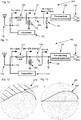
- Figures 3 and 4 respectively show a circuit diagram 200 of a first embodiment of parts of the receiver limb and the transmitter limb of the RF transceiver front end illustrated in Figure 1 in a receive mode of operation and a transmit mode of operation.
- the shunt switch 126 in a receive mode of operation, is open (and providing an open circuit) and as illustrated in Figure 4 , in the transmit mode of operation, the shunt switch 126 is closed (and providing substantially a short circuit).
- the impedance matching network 124 is configured to have a low pass performance.
- the impedance matching network includes a capacitance 210 arranged in parallel and connected to ground and an inductance arranged in series 212 and downstream of the capacitance.
- the pre-matching network 128 is configured to transform the input impedance of the low noise amplifier 130 to 10 ⁇ .
- the low pass LC network 124 When operating in the receiver mode as illustrated in Figure 3 , the low pass LC network 124 transforms 10 ⁇ to 50 ⁇ and hence the input impedance Z in to the impedance matching network 124 is 50 ⁇ .
- the same low pass LC network 124 transforms the low impedance (almost short provided by the closed shunt switch 126) to j*100 ⁇ .
- a transmission line with 0.07 ⁇ of physical length is enough to transform j*100 ⁇ to high impedance (almost open circuit) and hence the input impedance Z in for the transmission line 122 and receiver limb in the transmitter mode is very large and almost open circuit.
- the physical length of the transmission line 122 in this example is only 28% (i.e. 0.07/0.25 ⁇ 28%).
- Figure 5 shows a plot of the range of input impedances of the pre-matching network in a Smith Chart 220 fulfilling this criterion, and wherein the shadow area 222 in Figure 5 shows the values of Zpm which can work with the low pass impedance matching network 124 shown in Figures 3 and 4 to decrease the length of the transmission line 122 below ⁇ /4.
- the length of the transmission line 122 can be reduced to zero and hence the transmission line 122 can be omitted form the receiver limb 120.
- the impedance matching network LC circuit resonates at the operational frequency in the transmitter mode, and the transmission line length is shrunk to zero and so the transmission line 122 can be omitted.
- Figure 6 shows a Smith Chart 230 including a plot 232 of the range of impedance values for Zpm which can work with the impedance matching network 1234 of Figures 3 and 4 to allow the transmission line 122 to be omitted.
- Figures 7 and 8 respectively show a circuit diagram 240 of a second embodiment of parts of the receiver limb and the transmitter limb of the RF transceiver front end illustrated in Figure 1 in a receive mode of operation and a transmit mode of operation.
- the shunt switch 126 in a receive mode of operation, is open (and providing an open circuit) and as illustrated in Figure 8 , in the transmit mode of operation, the shunt switch 126 is closed (and providing substantially a short circuit).
- the impedance matching network 124 is again configured to have a low pass performance.
- the impedance matching network includes an inductance 232 arranged in series and a capacitance 244 connected to ground in parallel and downstream of the inductance 244.
- Figure 9 shows a Smith Chart 250, including an area 252 showing the values of Zpm which can work with the low pass impedance matching network 124 of Figures 7 and 8 to decrease the length of the transmission line 122 below ⁇ /4.
- Figures 10 and 11 respectively show a circuit diagram 260 of a third embodiment of parts of the receiver limb and the transmitter limb of the RF transceiver front end illustrated in Figure 1 in a receive mode of operation and a transmit mode of operation, similar to the first and second embodiments.
- the impedance matching network 124 is configured to have a high pass performance.
- the impedance matching network 124 includes an inductance 262 arranged in parallel and connected to ground and a capacitance 264 connected in series and downstream of the inductance 262.
- Figure 12 shows a Smith Chart 270, including an area 272 showing the values of Zpm which can work with the high pass impedance matching network 124 of Figures 10 and 11 to decrease the length of the transmission line 122 below ⁇ /4.
- Figure 13 shows a Smith Chart 280, including a line 280 showing the values of Zpm which can work with the high pass impedance matching network 124 of Figures 10 and 11 to shrink the length of the transmission line 122 to zero and hence allow the transmission line to be omitted.
- the pre-matching network 128 may be omitted.
- the impedance matching network 124 is configured to transform the input impedance of the low noise amplifier, Z lna to the input impedance of the transmission line or receiver limb in receiver mode (50 ⁇ in the above examples) and to transform 0 ⁇ to high impedance (open circuit) in transmitter mode.
- the RF transceiver front end 100 illustrated in Figures 1 and 2 can be provided in the form of an integrated circuit in a package.
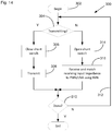
- Figure 14 shows a flow chart 300 illustrating a method of operation of the RF transceiver front end.
- the method begins 302 with operation of the overall system of which the RF transceiver front end 100 forms a part.
- the system determines whether the front-end is to be used in a transmitting or receiving mode. It is determined that the front end is to be used for transmitting, then at 306 the shunt switch is closed or is maintained closed if already closed and the transmitting limb is used for transmission at 308.
- the short circuit provided by the closed shunt switch is effectively transformed into an open circuit input impedance for the receiving limb by the impedance matching network and hence very little if any of the signal to be transmitted can leak into the receiving limb.
- the processing returns as illustrated by process flow 312 line back to 304 at which it is determined again whether the system is transmitting or receiving. If the system is receiving, then at 314, the shunt switch is opened, if previously closed, or maintained open, if previously open, and at 316, the input impedance of the receiving limb is matched to the input impedance of the downstream parts of the receiving limb, e.g. low noise amplifier 130 or pre-matching network 128, when provided, by the impedance matching network 124. Hence, the received RF signal is efficiently introduced into the receiving limb and downstream components owing to the good input impedance match between them.
- the shunt switch is opened, if previously closed, or maintained open, if previously open, and at 316, the input impedance of the receiving limb is matched to the input impedance of the downstream parts of the receiving limb, e.g. low noise amplifier 130 or pre-matching network 128, when provided, by the impedance matching network 124.
- the method may then continue and repeat by the system controlling the opening and closing of the shunt switch depending on whether the transceiver is in a receive or transmit mode of operation.
- the technique described herein can be used in the front end of any time division duplex (TDD) system operating at high frequency.
- TDD time division duplex
- This technique expands the operational frequency of a ⁇ /4 type switch from very high frequencies (>60 GHz) to lower frequencies as it allows the length of the transmission line to be reduced, in some cases to zero, and reduces insertion loss and improves the noise figure of the receiver.
- the reduced physical size of the transmission line also improves the ease with which the front end may be implemented as an integrated circuit.
Landscapes
- Engineering & Computer Science (AREA)
- Power Engineering (AREA)
- Computer Networks & Wireless Communication (AREA)
- Signal Processing (AREA)
- Microelectronics & Electronic Packaging (AREA)
- Transceivers (AREA)
- Transmitters (AREA)
Abstract
Description
- The present specification relates to switching radio frequency (RF) signals and in particular to switching in RF transceiver front ends.
- RF signals are used in a variety of applications and can give rise to a number of problems many of which may be related to the relatively high frequency of RF signals, often in the GHz part of the RF frequency range.
- RF signals can be particularly useful in wireless communications applications including various applications in so called 5G (5th generation) communications.
- For example radio frequency (RF) switches are used in the RF transceiver front-end and need to be able to withstand the worst case maximum voltage swing during the signal transmission. Due to the breakdown voltage limit of individual transistors for switching, some RF transceiver front-ends commonly use a stack of multiple switching transistors in series to withstand the large voltage swing during transmission. However, with more stacked transistor switches, insertion loss will increase which degrades the total noise figure of the receiving limb of the transceiver.
- An alternative approach is to use a quarter wavelength (λ/4) switch so as to avoid using the series multiple stacked transistors in the receiver limb and to ensure large signal swing sustainability. However, a drawback of a λ/4 switch is that they are suitable for use only at higher operational frequencies (for example greater than about 60 GHz). When the operational frequency is lower, then the physical length of transmission line needed to implement the λ/4 switch becomes longer. Hence, the physical transmission line increases in size and has a high insertion loss and hence degrades the receiver noise figure.
- Hence, a switchable RF transceiver front end having good performance in the receiver limb would be beneficial.
- According to a first aspect of the present disclosure, there is provided an RF transceiver front end having an operating frequency, comprising: a receiver limb including a length of transmission line, an impedance matching network, a shunt switch arranged downstream of the impedance matching network and a further receiver component arranged downstream of the shunt switch, wherein the receiver limb has a receiver limb input impedance and the further receiver component has a further receiver component input impedance; and a transmitter limb, wherein the impedance matching network is configured to transform the further receiver component input impedance to match the receiver limb input impedance when the shunt switch is open and the RF transceiver front end is operable in receiver mode and wherein the impedance matching network is further configured to transform the input impedance of the shunt switch to present an open circuit as the receiver limb input impedance when the shunt switch is closed and the RF transceiver front end is operable in transmitter mode and the length of transmission line is less than λ/4 for the operating frequency.
- In one or more embodiments, the further receiver component may be a low noise amplifier and the further receiver component input impedance may be a low noise amplifier input impedance.
- In one or more embodiments, the further receiver component may be a pre-matching network and the receiver limb may further include a low noise amplifier arranged downstream of pre-matching network and wherein further receiver component input impedance is a pre-matching network input impedance.
- In one or more embodiments, the impedance matching network may be configured to act as a low pass network. The low pass network may have a cut off frequency at least equal to or greater than the operating frequency. The low pass network may have a resonant frequency at least equal to or greater than the operating frequency.
- In one or more embodiments, the impedance matching network may include an inductance arranged in series and a capacitance arranged in parallel.
- In one or more embodiments, the capacitance may be upstream of the inductance or the capacitance may be downstream of the inductance.
- In one or more embodiments, the impedance matching network may be configured to act as a high pass network. The high pass network may have a cut off frequency at least equal to or greater than the operating frequency. The high pass network may have a resonant frequency at least equal to or greater than the operating frequency.
- In one or more embodiments, the impedance matching network may include a capacitance arranged in series and an inductance arranged in parallel.
- In one or more embodiments, the inductance may be upstream of the capacitance or the inductance may be downstream of the capacitance.
- In one or more embodiments, the length of transmission line is zero.
- In one or more embodiments, the operating frequency is less than 60GHz, 50GHz or 40GHz.
- In one or more embodiments, the operating frequency is greater than 20GHz.
- In one or more embodiments, the operating frequency is within the range of 10GHz to 100GHz.
- In one or more embodiments, the operating frequency is within the range of 20GHz to 50GHz.
- In one or more embodiments, the operating frequency is within the range of 24GHz to 45GHz.
- According to a second aspect of the present disclosure, there is provided a package including an integrated circuit, wherein the integrated circuit is configured to provide the RF transceiver front end of the first aspect and any preferred features thereof.
- In one or more embodiments, the package may be a front end integrated circuit (FEIC), and in particular may be a mm wave FEIC.
- According to a third aspect of the present disclosure, there is provided a wireless communication device or system including the RF transceiver front end of the first aspect or the package of the second aspect.
- In one or more embodiments, the wireless communication device or system may be a time division duplex communication device or system.
- According to a fourth aspect of the present disclosure, there is provided a method of operating an RF transceiver front end having a receiver limb and a transmitter limb connected to a common antenna, wherein the receiver limb includes a shunt switch arranged down stream of an impedance matching network and a further receiver component downstream of the shunt switch, comprising: opening a shunt switch in the receiver limb and matching the input impedance of the receiver limb to the input impedance of the further receiver component using the impedance matching network while receiving; and closing the shunt switch in the receiver limb and transforming the input impedance of the shunt switch to present an open circuit as the input impedance of the receiver limb using the impedance matching network while transmitted.
- Features of the first aspect may also be counterpart features for the fourth aspect.
- Embodiments of the invention will now be described in detail, by way of example only, and with reference to the accompanying drawings, in which:
-
Figure 1 shows a schematic block diagram of a first RF transceiver front end according to the invention; -
Figure 2 shows a schematic block diagram of a second RF transceiver front end according to the invention; -
Figure 3 shows a circuit diagram of a first embodiment of a part of the RF transceiver front end shown inFigure 2 in a receive mode of operation; -
Figure 4 shows the circuit diagram ofFigure 3 in a transmit mode of operation; -
Figure 5 shows a Smith chart illustrating possible ranges of values of the input impedance of the pre-matching network of the circuit shown inFigures 3 and 4 ; -
Figure 6 shows a Smith chart illustrating a particular value of the input impedance of the pre-matching network of the circuit shown inFigures 3 and 4 ; -
Figure 7 shows a circuit diagram of a second embodiment of a part of the RF transceiver front end shown inFigure 1 in a receive mode of operation; -
Figure 8 shows the circuit diagram ofFigure 7 in a transmit mode of operation; -
Figure 9 shows a Smith chart illustrating possible ranges of values of the input impedance of the pre-matching network of the circuit shown inFigures 7 and 8 ; -
Figure 10 shows a circuit diagram of a third embodiment of a part of the RF transceiver front end shown inFigure 1 in a receive mode of operation; -
Figure 11 shows the circuit diagram ofFigure 10 in a transmit mode of operation; -
Figure 12 shows a Smith chart illustrating possible ranges of values of the input impedance of the pre-matching network of the circuit shown inFigures 9 and10 ; -
Figure 13 shows a Smith chart illustrating possible values of the input impedance of the pre-matching network of the circuit shown inFigures 9 and10 ; and -
Figure 14 shows a flow chart illustrating a method of operation of the RF transceiver front end. - Similar items in the different Figures share like reference signs unless indicated otherwise.
- With reference to
Figure 1 there is shown a schematic block diagram of an RF transceiverfront end device 100 attached to anantenna 102. Thefront end device 100 may be in the form of an integrated circuit provided in a package. In other embodiments, theantenna 102 may also be provided as part of the integratedcircuit 100. The RF transceiver front end, also sometimes referred to simply as a front end IC, also has aconnection 104 for receiving and passing RF signals from other parts of a larger system which are to be transmitted via theantenna 102 or which have been received by theantenna 102. The RF signals may generally be in the range of about 20GHz to 60GHz. - For example, front end may be used for devices and systems complying in the 5G mm wave frequency range of 24GHz to 45GHz.
- However, the approach can be applied more generally at frequencies high enough to allow for efficient silicon implementation, in general from 20GHz upwards.
- In some applications, e.g. phased antenna arrays, there may be a plurality of RF transceiver front ends each with a respective antenna and respective RF connection. One or more RF transceiver front-ends may be used in various application, including 5G telecommunications. The approach described herein also may be used in applications based on phased array concepts, FEICs for 60GHz communication standards and also for E-band communication at 85GHz.
- The RF transceiver
front end device 100 includes atransmission limb 110 which connected between anantenna connection 103 for theantenna 102 and anRF connection switch 106 and also areception limb 120 also connected between theantenna connection 103 and theRF connection switch 106. TheRF connection switch 106 is used to selectively provide a signal path between the antenna and RF connection via either thetransmission limb 110 or thereception limb 120. - The
transmission limb 110 can includevarious components 112 as commonly provided in a transceiver and are not the focus of the present invention. For example, as illustrated inFigure 1 , the transmission components in the transmission limb may include atransmitter power amplifier 114 configured to increase the power of the RF signal prior to transmission by the antenna and also atransmitter switch 116. The transmitter switch may be operable to connect thepower amplifier 114 to theantenna 102 during a transmission mode of operation and to isolate thepower amplifier 114 form theantenna 102 during a reception mode of operation. - The
reception limb 120 can also include various components some of which may be commonly provided in a transceiver and others of which form part of the invention as explained below. - The
reception limb 120 includes a length oftransmission line 122 connected to theantenna connection 103. Unlike previous RF transceiver front ends, thetransmission line 122 has a length less than a quarter wavelength, λ/4, at the operating frequency of the RF transceiver front end. Animpedance matching circuit 124 is provided downstream of the transmission line and then ashunt switch 126 connected to ground is provided downstream of theimpedance matching network 124. In the embodiment illustrated inFigure 1 , a pre-matching network is provided downstream of theshunt switch 126 and before anamplifier 130, which may be a low noise amplifier. An output of thelow noise amplifier 130 is connected to an input of avariable gain amplifier 132, the output of which is connected to a vector modulator orphase shifter 134, the output of which is connected to theRF switch 106. -
Figure 2 shows a schematic block diagram of a second RF transceiver front end device 100' generally similar to that shown inFigure 1 . However, in the second RF transceiver front end device 100', there is nopre-matching network 128 between theshunt switch 126 and theamplifier 130. Hence, in some embodiments of the invention, depending on a number of factors and including the input impedance presented by theamplifier 130, apre-matching network 128 may not be used. - It will be appreciated that the specific receiver and transmitter components illustrated in
Figures 1 and 2 are by way of example only and that the approach is not limited to those specific transmitter and receiver component arrangements. Rather the approach described herein relates more to theconnection 103 between the transmitter and receiver limbs of the transceiver. - The illustrated line-up of
impedance matching network 124,shunt switch 126 andamplifier 130 may be used to decrease the physical length of thetransmission line 122 in the receiver limb to be less than λ/4 and, under some certain circumstances, thetransmission line 122 can even be omitted from the receiver limb. With decreased physical length of the transmission line, thetransmission line 122 has a smaller size, thereceiver limb 120 has lower insertion loss and also an improved receiver noise figure. Also this approach can invention expands the operational frequency of the RF transceiver front end device to lower frequencies, for example of the order of a few GHz, e.g. 100Hz. An upper end on the range of application may be about 100GHz. - In the receiver limb, the
shunt switch 126 is applied downstream of theimpedance matching network 124 and between theimpedance matching network 124 and either apre-matching network 128, when used, or theamplifier 130. During a receiver mode of operation, withshunt switch 126 open, thepre-matching network 128 transforms the input impedance of theamplifier 130 to a specified impedance (Zpm) and theimpedance matching network 124 transforms Zpm to 50 Ω, being the impedance of thetransmission line 122. In a transmitter mode of operation, withshunt switch 126 closed, theimpedance matching network 124 transforms a very low impedance (≈ 0 Ω), provided by theclosed shunt switch 126, to an inductive impedance, which decreases the physical length of transmission line that need so to be provided in order to realize an open circuit input impedance for thereceiver limb 120 and hence effectively block leakage of high power RF signals into thereceiver limb 120. - Generally, the specific value of the input impedance of the pre-matching network Zpm is not limited to a single value and may have a range of values. The specific topology of the
impedance matching network 124 influences the range of values of Zpm and also the physical length oftransmission line 122, as described in greater detail below. As noted above, the pre-matching network is optional and in some cases may be omitted entirely, when the input impedance of the amplifier naturally satisfies the requirement of the value of Zpm. Also, the technique is IC technology independent and can be applied for example in CMOS, BiMCOS as well as GaAs solutions -
Figures 3 and 4 respectively show a circuit diagram 200 of a first embodiment of parts of the receiver limb and the transmitter limb of the RF transceiver front end illustrated inFigure 1 in a receive mode of operation and a transmit mode of operation. As illustrated inFigure 3 , in a receive mode of operation, theshunt switch 126 is open (and providing an open circuit) and as illustrated inFigure 4 , in the transmit mode of operation, theshunt switch 126 is closed (and providing substantially a short circuit). Theimpedance matching network 124 is configured to have a low pass performance. In particular, the impedance matching network includes acapacitance 210 arranged in parallel and connected to ground and an inductance arranged inseries 212 and downstream of the capacitance. - The decrease of the physical length of the
transmission line 122 to less than in λ/4 will now be explained. To simplify the explanation, it is assumed that thepre-matching network 128 is configured to transform the input impedance of thelow noise amplifier 130 to 10 Ω. - When operating in the receiver mode as illustrated in
Figure 3 , the lowpass LC network 124 transforms 10 Ω to 50 Ω and hence the input impedance Zin to theimpedance matching network 124 is 50Ω. In transmitter mode as illustrated inFigure 4 , the same lowpass LC network 124 transforms the low impedance (almost short provided by the closed shunt switch 126) to j*100 Ω. Thus, a transmission line with 0.07λ of physical length is enough to transform j*100 Ω to high impedance (almost open circuit) and hence the input impedance Zin for thetransmission line 122 and receiver limb in the transmitter mode is very large and almost open circuit. Compared to a λ/4 length transmission line approach, the physical length of thetransmission line 122 in this example is only 28% (i.e. 0.07/0.25 ≈ 28%). - For the low pass
impedance matching network 124 shown inFigures 3 and 4 , the requirement of the input impedance for thepre-matching network 128 is Zin = Zpm = Rpm + j*Xpm, where Rpm is the resistance of thepre-matching network 128 and Xpm is the reactance of thepre-matching network 128. Since theimpedance matching network 124 transforms Zpm to 50 Ω in receiver mode and 0 Ω to inductive in transmitter mode, respectively:

-
Figure 5 shows a plot of the range of input impedances of the pre-matching network in aSmith Chart 220 fulfilling this criterion, and wherein theshadow area 222 inFigure 5 shows the values of Zpm which can work with the low passimpedance matching network 124 shown inFigures 3 and 4 to decrease the length of thetransmission line 122 below λ/4. - As noted above, in some circumstances the length of the
transmission line 122 can be reduced to zero and hence thetransmission line 122 can be omitted form thereceiver limb 120. - If, in
Figures 3 and 4 , theimpedance matching network 124 transforms the input impedance of thepre-matching network 128 Zpm to 50 Ω in receiver mode (Fig. 3 ) and transforms 0 Ω to high impedance (open circuit) in transmitter mode (Fig. 4 ), then:

- In this case, the impedance matching network LC circuit resonates at the operational frequency in the transmitter mode, and the transmission line length is shrunk to zero and so the
transmission line 122 can be omitted. -
Figure 6 shows aSmith Chart 230 including aplot 232 of the range of impedance values for Zpm which can work with the impedance matching network 1234 ofFigures 3 and 4 to allow thetransmission line 122 to be omitted. -
Figures 7 and 8 respectively show a circuit diagram 240 of a second embodiment of parts of the receiver limb and the transmitter limb of the RF transceiver front end illustrated inFigure 1 in a receive mode of operation and a transmit mode of operation. As illustrated inFigure 7 , in a receive mode of operation, theshunt switch 126 is open (and providing an open circuit) and as illustrated inFigure 8 , in the transmit mode of operation, theshunt switch 126 is closed (and providing substantially a short circuit). Theimpedance matching network 124 is again configured to have a low pass performance. In particular, the impedance matching network includes aninductance 232 arranged in series and acapacitance 244 connected to ground in parallel and downstream of theinductance 244. - Similarly to the first embodiment, the low pass
impedance matching network 124 transforms Zpm to 50Ω in receiver mode (Fig. 7 ) and transforms 0Ω to high impedance (open circuit) in transmitter mode (Fig. 8 ):

-
Figure 9 shows aSmith Chart 250, including anarea 252 showing the values of Zpm which can work with the low passimpedance matching network 124 ofFigures 7 and 8 to decrease the length of thetransmission line 122 below λ/4. -
Figures 10 and 11 respectively show a circuit diagram 260 of a third embodiment of parts of the receiver limb and the transmitter limb of the RF transceiver front end illustrated inFigure 1 in a receive mode of operation and a transmit mode of operation, similar to the first and second embodiments. In the third embodiment, theimpedance matching network 124 is configured to have a high pass performance. In particular, theimpedance matching network 124 includes aninductance 262 arranged in parallel and connected to ground and acapacitance 264 connected in series and downstream of theinductance 262. - Similarly to the first and second embodiments, the low pass
impedance matching network 124 transforms Zpm to 50Ωin receiver mode (Fig. 10 ) and transforms 0Ω to high impedance (open circuit) in transmitter mode (Fig. 11 ):

-
Figure 12 shows a Smith Chart 270, including anarea 272 showing the values of Zpm which can work with the high passimpedance matching network 124 ofFigures 10 and 11 to decrease the length of thetransmission line 122 below λ/4. - The condition to shrink the length of the
transmission line 122 to zero and hence omit the transmission line is:
-
Figure 13 shows aSmith Chart 280, including aline 280 showing the values of Zpm which can work with the high passimpedance matching network 124 ofFigures 10 and 11 to shrink the length of thetransmission line 122 to zero and hence allow the transmission line to be omitted. - As discussed above, and as illustrated in
Figure 2 , in some embodiments, thepre-matching network 128 may be omitted. In that case, theimpedance matching network 124 is configured to transform the input impedance of the low noise amplifier, Zlna to the input impedance of the transmission line or receiver limb in receiver mode (50Ω in the above examples) and to transform 0Ω to high impedance (open circuit) in transmitter mode. - In some embodiments, the RF transceiver
front end 100 illustrated inFigures 1 and 2 can be provided in the form of an integrated circuit in a package. -
Figure 14 shows aflow chart 300 illustrating a method of operation of the RF transceiver front end. The method begins 302 with operation of the overall system of which the RF transceiverfront end 100 forms a part. At 304 the system determines whether the front-end is to be used in a transmitting or receiving mode. It is determined that the front end is to be used for transmitting, then at 306 the shunt switch is closed or is maintained closed if already closed and the transmitting limb is used for transmission at 308. As explained above, the short circuit provided by the closed shunt switch is effectively transformed into an open circuit input impedance for the receiving limb by the impedance matching network and hence very little if any of the signal to be transmitted can leak into the receiving limb. - If operation of the system is determined at 310 to be continuing, the processing returns as illustrated by
process flow 312 line back to 304 at which it is determined again whether the system is transmitting or receiving. If the system is receiving, then at 314, the shunt switch is opened, if previously closed, or maintained open, if previously open, and at 316, the input impedance of the receiving limb is matched to the input impedance of the downstream parts of the receiving limb, e.g.low noise amplifier 130 orpre-matching network 128, when provided, by theimpedance matching network 124. Hence, the received RF signal is efficiently introduced into the receiving limb and downstream components owing to the good input impedance match between them. - The method may then continue and repeat by the system controlling the opening and closing of the shunt switch depending on whether the transceiver is in a receive or transmit mode of operation.
- The technique described herein can be used in the front end of any time division duplex (TDD) system operating at high frequency. In such systems a certain switch functionality needs to be present at the antenna port, to enable receive or transmit. This technique expands the operational frequency of a λ/4 type switch from very high frequencies (>60 GHz) to lower frequencies as it allows the length of the transmission line to be reduced, in some cases to zero, and reduces insertion loss and improves the noise figure of the receiver. The reduced physical size of the transmission line also improves the ease with which the front end may be implemented as an integrated circuit.
- In this specification, example embodiments have been presented in terms of a selected set of details. However, a person of ordinary skill in the art would understand that many other example embodiments may be practiced which include a different selected set of these details. It is intended that the following claims cover all possible example embodiments.
- Any instructions and/or flowchart steps can be executed in any order, unless a specific order is explicitly stated. Also, those skilled in the art will recognize that while one example set of instructions/method has been discussed, the material in this specification can be combined in a variety of ways to yield other examples as well, and are to be understood within a context provided by this detailed description.
- While the disclosure is amenable to various modifications and alternative forms, specifics thereof have been shown by way of example in the drawings and described in detail. It should be understood, however, that other embodiments, beyond the particular embodiments described, are possible as well. All modifications, equivalents, and alternative embodiments falling within the scope of the appended claims are covered as well.
Claims (14)
- An RF transceiver front end having an operating frequency, comprising:a receiver limb including a length of transmission line, an impedance matching network, a shunt switch arranged downstream of the impedance matching network and a further receiver component arranged downstream of the shunt switch, wherein the receiver limb has a receiver limb input impedance and the further receiver component has a further receiver component input impedance; anda transmitter limb, wherein the impedance matching network is configured to transform the further receiver component input impedance to match the receiver limb input impedance when the shunt switch is open and the RF transceiver front end is operable in receiver mode and wherein the impedance matching network is further configured to transform the input impedance of the shunt switch to present an open circuit as the receiver limb input impedance when the shunt switch is closed and the RF transceiver front end is operable in transmitter mode and the length of transmission line is less than λ/4 for the operating frequency.
- The RF transceiver front end as claimed in claim 1, wherein the further receiver component is a low noise amplifier and the further receiver component input impedance is a low noise amplifier input impedance.
- The RF transceiver front end as claimed in claim 1, wherein the further receiver component is pre-matching network and the receiver limb further includes a low noise amplifier arranged downstream of pre-matching network and wherein further receiver component input impedance is a pre-matching network input impedance.
- The RF transceiver front end as claimed in any of claims 1 to 3, wherein the impedance matching network is configured to act as a low pass network.
- The RF transceiver front end as claimed in claim 4, wherein the impedance matching network includes an inductance arranged in series and a capacitance arranged in parallel.
- The RF transceiver front end as claimed in claim 5, wherein the capacitance is upstream of the inductance or the capacitance is downstream of the inductance.
- The RF transceiver front end as claimed in any of claims 1 to 3, wherein the impedance matching network is configured to act as a high pass network.
- The RF transceiver front end as claimed in claim 7, wherein the impedance matching network includes a capacitance arranged in series and an inductance arranged in parallel.
- The RF transceiver front end as claimed in claim 8, wherein the inductance is upstream of the capacitance or the inductance is downstream of the capacitance.
- The RF transceiver front end as claimed in any of claim 1 to 9, wherein the length of transmission line is zero.
- The RF transceiver front end as claimed in any of claims 1 to 10, wherein the operating frequency is less than 40GHz.
- A package including an integrated circuit, wherein the integrated circuit is configured to provide the RF transceiver front end of any of claims 1 to 11.
- A time division duplex communication system including the RF transceiver front end of any of claims 1 to 11 or the package of claim 12.
- A method of operating an RF transceiver front end having a receiver limb and a transmitter limb connected to a common antenna, wherein the receiver limb includes a shunt switch arranged down stream of an impedance matching network and a further receiver component downstream of the shunt switch, comprising:opening a shunt switch in the receiver limb and matching the input impedance of the receiver limb to the input impedance of the further receiver component using the impedance matching network while receiving; andclosing the shunt switch in the receiver limb and transforming the input impedance of the shunt switch to present an open circuit as the input impedance of the receiver limb using the impedance matching network while transmitted.
Priority Applications (3)
| Application Number | Priority Date | Filing Date | Title |
|---|---|---|---|
| EP18187712.7A EP3609085B1 (en) | 2018-08-07 | 2018-08-07 | Rf switching |
| US16/514,227 US11539333B2 (en) | 2018-08-07 | 2019-07-17 | RF switching |
| CN201910728290.4A CN110858771B (en) | 2018-08-07 | 2019-08-07 | RF switching |
Applications Claiming Priority (1)
| Application Number | Priority Date | Filing Date | Title |
|---|---|---|---|
| EP18187712.7A EP3609085B1 (en) | 2018-08-07 | 2018-08-07 | Rf switching |
Publications (2)
| Publication Number | Publication Date |
|---|---|
| EP3609085A1 true EP3609085A1 (en) | 2020-02-12 |
| EP3609085B1 EP3609085B1 (en) | 2021-02-24 |
Family
ID=63311783
Family Applications (1)
| Application Number | Title | Priority Date | Filing Date |
|---|---|---|---|
| EP18187712.7A Active EP3609085B1 (en) | 2018-08-07 | 2018-08-07 | Rf switching |
Country Status (3)
| Country | Link |
|---|---|
| US (1) | US11539333B2 (en) |
| EP (1) | EP3609085B1 (en) |
| CN (1) | CN110858771B (en) |
Cited By (1)
| Publication number | Priority date | Publication date | Assignee | Title |
|---|---|---|---|---|
| US12574066B2 (en) * | 2020-09-30 | 2026-03-10 | Telefonaktiebolaget Lm Ericsson (Publ) | Transceiver switch circuitry |
Families Citing this family (9)
| Publication number | Priority date | Publication date | Assignee | Title |
|---|---|---|---|---|
| US11063355B2 (en) * | 2019-03-04 | 2021-07-13 | Tubis Technology Inc. | Bi-directional vector modulator/active phase shifter |
| US11652504B2 (en) * | 2019-08-13 | 2023-05-16 | Skyworks Solutions, Inc. | Fast antenna switching |
| WO2022069038A1 (en) * | 2020-09-30 | 2022-04-07 | Telefonaktiebolaget Lm Ericsson (Publ) | A transceiver switch circuitry |
| EP3985881B1 (en) | 2020-10-15 | 2023-06-07 | IMEC vzw | Wideband radio-frequency transceiver front-end and operation method thereof |
| US12413259B2 (en) | 2020-11-27 | 2025-09-09 | Telefonaktiebolaget Lm Ericsson (Publ) | Differential transceiver switch circuitry |
| EP4137836B1 (en) | 2021-08-20 | 2025-07-02 | Nxp B.V. | Communication device and corresponding operating method |
| KR20230029413A (en) | 2021-08-24 | 2023-03-03 | 삼성전자주식회사 | A transceiver using active device and antenna module including the same |
| CN115685029B (en) * | 2022-11-07 | 2026-04-17 | 华东师范大学 | A self-generating and self-receiving coil and its working method |
| EP4447327B1 (en) | 2023-04-14 | 2026-02-18 | EM Microelectronic-Marin SA | Impedance matching network |
Citations (2)
| Publication number | Priority date | Publication date | Assignee | Title |
|---|---|---|---|---|
| US20140206301A1 (en) * | 2012-03-27 | 2014-07-24 | Hemasundar Mohan Geddada | Transceiver with an integrated rx/tx configurable passive network |
| US9559747B1 (en) * | 2015-10-13 | 2017-01-31 | International Business Machines Corporation | Efficient transmit and receive switches |
Family Cites Families (4)
| Publication number | Priority date | Publication date | Assignee | Title |
|---|---|---|---|---|
| US6356536B1 (en) * | 1998-09-30 | 2002-03-12 | Ericsson Inc. | Protective and decoupling shunt switch at LNA input for TDMA/TDD transceivers |
| US8989678B2 (en) * | 2011-06-30 | 2015-03-24 | Mediatek Inc. | Transceiver and method thereof |
| US9184722B2 (en) * | 2012-02-10 | 2015-11-10 | Infineon Technologies Ag | Adjustable impedance matching network |
| US9479126B2 (en) * | 2014-08-19 | 2016-10-25 | Infineon Technologies Ag | System and method for a low noise amplifier |
-
2018
- 2018-08-07 EP EP18187712.7A patent/EP3609085B1/en active Active
-
2019
- 2019-07-17 US US16/514,227 patent/US11539333B2/en active Active
- 2019-08-07 CN CN201910728290.4A patent/CN110858771B/en active Active
Patent Citations (2)
| Publication number | Priority date | Publication date | Assignee | Title |
|---|---|---|---|---|
| US20140206301A1 (en) * | 2012-03-27 | 2014-07-24 | Hemasundar Mohan Geddada | Transceiver with an integrated rx/tx configurable passive network |
| US9559747B1 (en) * | 2015-10-13 | 2017-01-31 | International Business Machines Corporation | Efficient transmit and receive switches |
Cited By (1)
| Publication number | Priority date | Publication date | Assignee | Title |
|---|---|---|---|---|
| US12574066B2 (en) * | 2020-09-30 | 2026-03-10 | Telefonaktiebolaget Lm Ericsson (Publ) | Transceiver switch circuitry |
Also Published As
| Publication number | Publication date |
|---|---|
| CN110858771B (en) | 2023-05-16 |
| EP3609085B1 (en) | 2021-02-24 |
| US11539333B2 (en) | 2022-12-27 |
| CN110858771A (en) | 2020-03-03 |
| US20200059208A1 (en) | 2020-02-20 |
Similar Documents
| Publication | Publication Date | Title |
|---|---|---|
| US11539333B2 (en) | RF switching | |
| US12237821B2 (en) | Adaptive tuning networks with direct mapped multiple channel filter tuning | |
| CN111585583B (en) | Adaptive tuning network for combinable filters | |
| US8416035B2 (en) | Multiband matching circuit | |
| US11967977B2 (en) | Switch circuit, radio frequency front-end circuit, and communication device | |
| US10985734B2 (en) | Radio frequency switch | |
| WO2002067451A1 (en) | Switch device and portable communication terminal | |
| CN116232259B (en) | Radio frequency front end, radio frequency circuit and chip based on back matching architecture | |
| US10666231B2 (en) | Balun arrangement | |
| US10511344B1 (en) | Transceiver resonant receive switch | |
| US12142809B2 (en) | Bidirectional RF coupler with switchable coupled transmission lines for operation over different frequency bands | |
| US12556142B2 (en) | Reconfigurable and tunable power amplifier | |
| US8149071B2 (en) | Radio frequency switch and apparatus containing the radio frequency switch | |
| US9685990B2 (en) | Methods and devices for overcoming insertion loss in RF systems | |
| EP1772964B1 (en) | High-frequency switch circuit | |
| Renström et al. | RF Front-End Building Blocks for 6G cmWave Radio Base Station in 300 mm GaN-on-Si Technology | |
| JPWO2019207836A1 (en) | High frequency switch and antenna device | |
| US10312961B1 (en) | Transceiver resonant receive switch | |
| US20050253665A1 (en) | Automatic radio frequency signal controller device and associated method | |
| CN118901206A (en) | LNA with TX harmonic filter | |
| WO2023208320A1 (en) | Transceiver with antenna switch incorporating input impedance matching for receiver amplifier | |
| Lauder et al. | Recent Developments in Automatic Impedance Matching and Antenna Tuning for Wireless and Mobile Communications |
Legal Events
| Date | Code | Title | Description |
|---|---|---|---|
| PUAI | Public reference made under article 153(3) epc to a published international application that has entered the european phase |
Free format text: ORIGINAL CODE: 0009012 |
|
| STAA | Information on the status of an ep patent application or granted ep patent |
Free format text: STATUS: THE APPLICATION HAS BEEN PUBLISHED |
|
| AK | Designated contracting states |
Kind code of ref document: A1 Designated state(s): AL AT BE BG CH CY CZ DE DK EE ES FI FR GB GR HR HU IE IS IT LI LT LU LV MC MK MT NL NO PL PT RO RS SE SI SK SM TR |
|
| AX | Request for extension of the european patent |
Extension state: BA ME |
|
| STAA | Information on the status of an ep patent application or granted ep patent |
Free format text: STATUS: REQUEST FOR EXAMINATION WAS MADE |
|
| 17P | Request for examination filed |
Effective date: 20200812 |
|
| RBV | Designated contracting states (corrected) |
Designated state(s): AL AT BE BG CH CY CZ DE DK EE ES FI FR GB GR HR HU IE IS IT LI LT LU LV MC MK MT NL NO PL PT RO RS SE SI SK SM TR |
|
| GRAP | Despatch of communication of intention to grant a patent |
Free format text: ORIGINAL CODE: EPIDOSNIGR1 |
|
| STAA | Information on the status of an ep patent application or granted ep patent |
Free format text: STATUS: GRANT OF PATENT IS INTENDED |
|
| INTG | Intention to grant announced |
Effective date: 20201103 |
|
| GRAS | Grant fee paid |
Free format text: ORIGINAL CODE: EPIDOSNIGR3 |
|
| GRAA | (expected) grant |
Free format text: ORIGINAL CODE: 0009210 |
|
| STAA | Information on the status of an ep patent application or granted ep patent |
Free format text: STATUS: THE PATENT HAS BEEN GRANTED |
|
| AK | Designated contracting states |
Kind code of ref document: B1 Designated state(s): AL AT BE BG CH CY CZ DE DK EE ES FI FR GB GR HR HU IE IS IT LI LT LU LV MC MK MT NL NO PL PT RO RS SE SI SK SM TR |
|
| REG | Reference to a national code |
Ref country code: CH Ref legal event code: EP |
|
| REG | Reference to a national code |
Ref country code: AT Ref legal event code: REF Ref document number: 1365790 Country of ref document: AT Kind code of ref document: T Effective date: 20210315 |
|
| REG | Reference to a national code |
Ref country code: IE Ref legal event code: FG4D |
|
| REG | Reference to a national code |
Ref country code: DE Ref legal event code: R096 Ref document number: 602018012935 Country of ref document: DE |
|
| REG | Reference to a national code |
Ref country code: LT Ref legal event code: MG9D |
|
| REG | Reference to a national code |
Ref country code: NL Ref legal event code: MP Effective date: 20210224 |
|
| PG25 | Lapsed in a contracting state [announced via postgrant information from national office to epo] |
Ref country code: NO Free format text: LAPSE BECAUSE OF FAILURE TO SUBMIT A TRANSLATION OF THE DESCRIPTION OR TO PAY THE FEE WITHIN THE PRESCRIBED TIME-LIMIT Effective date: 20210524 Ref country code: PT Free format text: LAPSE BECAUSE OF FAILURE TO SUBMIT A TRANSLATION OF THE DESCRIPTION OR TO PAY THE FEE WITHIN THE PRESCRIBED TIME-LIMIT Effective date: 20210624 Ref country code: LT Free format text: LAPSE BECAUSE OF FAILURE TO SUBMIT A TRANSLATION OF THE DESCRIPTION OR TO PAY THE FEE WITHIN THE PRESCRIBED TIME-LIMIT Effective date: 20210224 Ref country code: FI Free format text: LAPSE BECAUSE OF FAILURE TO SUBMIT A TRANSLATION OF THE DESCRIPTION OR TO PAY THE FEE WITHIN THE PRESCRIBED TIME-LIMIT Effective date: 20210224 Ref country code: HR Free format text: LAPSE BECAUSE OF FAILURE TO SUBMIT A TRANSLATION OF THE DESCRIPTION OR TO PAY THE FEE WITHIN THE PRESCRIBED TIME-LIMIT Effective date: 20210224 Ref country code: GR Free format text: LAPSE BECAUSE OF FAILURE TO SUBMIT A TRANSLATION OF THE DESCRIPTION OR TO PAY THE FEE WITHIN THE PRESCRIBED TIME-LIMIT Effective date: 20210525 Ref country code: BG Free format text: LAPSE BECAUSE OF FAILURE TO SUBMIT A TRANSLATION OF THE DESCRIPTION OR TO PAY THE FEE WITHIN THE PRESCRIBED TIME-LIMIT Effective date: 20210524 |
|
| REG | Reference to a national code |
Ref country code: AT Ref legal event code: MK05 Ref document number: 1365790 Country of ref document: AT Kind code of ref document: T Effective date: 20210224 |
|
| PG25 | Lapsed in a contracting state [announced via postgrant information from national office to epo] |
Ref country code: SE Free format text: LAPSE BECAUSE OF FAILURE TO SUBMIT A TRANSLATION OF THE DESCRIPTION OR TO PAY THE FEE WITHIN THE PRESCRIBED TIME-LIMIT Effective date: 20210224 Ref country code: NL Free format text: LAPSE BECAUSE OF FAILURE TO SUBMIT A TRANSLATION OF THE DESCRIPTION OR TO PAY THE FEE WITHIN THE PRESCRIBED TIME-LIMIT Effective date: 20210224 Ref country code: PL Free format text: LAPSE BECAUSE OF FAILURE TO SUBMIT A TRANSLATION OF THE DESCRIPTION OR TO PAY THE FEE WITHIN THE PRESCRIBED TIME-LIMIT Effective date: 20210224 Ref country code: RS Free format text: LAPSE BECAUSE OF FAILURE TO SUBMIT A TRANSLATION OF THE DESCRIPTION OR TO PAY THE FEE WITHIN THE PRESCRIBED TIME-LIMIT Effective date: 20210224 Ref country code: LV Free format text: LAPSE BECAUSE OF FAILURE TO SUBMIT A TRANSLATION OF THE DESCRIPTION OR TO PAY THE FEE WITHIN THE PRESCRIBED TIME-LIMIT Effective date: 20210224 |
|
| PG25 | Lapsed in a contracting state [announced via postgrant information from national office to epo] |
Ref country code: IS Free format text: LAPSE BECAUSE OF FAILURE TO SUBMIT A TRANSLATION OF THE DESCRIPTION OR TO PAY THE FEE WITHIN THE PRESCRIBED TIME-LIMIT Effective date: 20210624 |
|
| PG25 | Lapsed in a contracting state [announced via postgrant information from national office to epo] |
Ref country code: AT Free format text: LAPSE BECAUSE OF FAILURE TO SUBMIT A TRANSLATION OF THE DESCRIPTION OR TO PAY THE FEE WITHIN THE PRESCRIBED TIME-LIMIT Effective date: 20210224 Ref country code: SM Free format text: LAPSE BECAUSE OF FAILURE TO SUBMIT A TRANSLATION OF THE DESCRIPTION OR TO PAY THE FEE WITHIN THE PRESCRIBED TIME-LIMIT Effective date: 20210224 Ref country code: EE Free format text: LAPSE BECAUSE OF FAILURE TO SUBMIT A TRANSLATION OF THE DESCRIPTION OR TO PAY THE FEE WITHIN THE PRESCRIBED TIME-LIMIT Effective date: 20210224 Ref country code: CZ Free format text: LAPSE BECAUSE OF FAILURE TO SUBMIT A TRANSLATION OF THE DESCRIPTION OR TO PAY THE FEE WITHIN THE PRESCRIBED TIME-LIMIT Effective date: 20210224 |
|
| REG | Reference to a national code |
Ref country code: DE Ref legal event code: R097 Ref document number: 602018012935 Country of ref document: DE |
|
| PG25 | Lapsed in a contracting state [announced via postgrant information from national office to epo] |
Ref country code: DK Free format text: LAPSE BECAUSE OF FAILURE TO SUBMIT A TRANSLATION OF THE DESCRIPTION OR TO PAY THE FEE WITHIN THE PRESCRIBED TIME-LIMIT Effective date: 20210224 Ref country code: RO Free format text: LAPSE BECAUSE OF FAILURE TO SUBMIT A TRANSLATION OF THE DESCRIPTION OR TO PAY THE FEE WITHIN THE PRESCRIBED TIME-LIMIT Effective date: 20210224 Ref country code: SK Free format text: LAPSE BECAUSE OF FAILURE TO SUBMIT A TRANSLATION OF THE DESCRIPTION OR TO PAY THE FEE WITHIN THE PRESCRIBED TIME-LIMIT Effective date: 20210224 |
|
| PLBE | No opposition filed within time limit |
Free format text: ORIGINAL CODE: 0009261 |
|
| STAA | Information on the status of an ep patent application or granted ep patent |
Free format text: STATUS: NO OPPOSITION FILED WITHIN TIME LIMIT |
|
| PG25 | Lapsed in a contracting state [announced via postgrant information from national office to epo] |
Ref country code: AL Free format text: LAPSE BECAUSE OF FAILURE TO SUBMIT A TRANSLATION OF THE DESCRIPTION OR TO PAY THE FEE WITHIN THE PRESCRIBED TIME-LIMIT Effective date: 20210224 Ref country code: ES Free format text: LAPSE BECAUSE OF FAILURE TO SUBMIT A TRANSLATION OF THE DESCRIPTION OR TO PAY THE FEE WITHIN THE PRESCRIBED TIME-LIMIT Effective date: 20210224 |
|
| 26N | No opposition filed |
Effective date: 20211125 |
|
| PG25 | Lapsed in a contracting state [announced via postgrant information from national office to epo] |
Ref country code: SI Free format text: LAPSE BECAUSE OF FAILURE TO SUBMIT A TRANSLATION OF THE DESCRIPTION OR TO PAY THE FEE WITHIN THE PRESCRIBED TIME-LIMIT Effective date: 20210224 |
|
| REG | Reference to a national code |
Ref country code: CH Ref legal event code: PL |
|
| PG25 | Lapsed in a contracting state [announced via postgrant information from national office to epo] |
Ref country code: MC Free format text: LAPSE BECAUSE OF FAILURE TO SUBMIT A TRANSLATION OF THE DESCRIPTION OR TO PAY THE FEE WITHIN THE PRESCRIBED TIME-LIMIT Effective date: 20210224 |
|
| REG | Reference to a national code |
Ref country code: BE Ref legal event code: MM Effective date: 20210831 |
|
| PG25 | Lapsed in a contracting state [announced via postgrant information from national office to epo] |
Ref country code: LI Free format text: LAPSE BECAUSE OF NON-PAYMENT OF DUE FEES Effective date: 20210831 Ref country code: IT Free format text: LAPSE BECAUSE OF FAILURE TO SUBMIT A TRANSLATION OF THE DESCRIPTION OR TO PAY THE FEE WITHIN THE PRESCRIBED TIME-LIMIT Effective date: 20210224 Ref country code: CH Free format text: LAPSE BECAUSE OF NON-PAYMENT OF DUE FEES Effective date: 20210831 |
|
| PG25 | Lapsed in a contracting state [announced via postgrant information from national office to epo] |
Ref country code: IS Free format text: LAPSE BECAUSE OF FAILURE TO SUBMIT A TRANSLATION OF THE DESCRIPTION OR TO PAY THE FEE WITHIN THE PRESCRIBED TIME-LIMIT Effective date: 20210624 Ref country code: LU Free format text: LAPSE BECAUSE OF NON-PAYMENT OF DUE FEES Effective date: 20210807 |
|
| PG25 | Lapsed in a contracting state [announced via postgrant information from national office to epo] |
Ref country code: IE Free format text: LAPSE BECAUSE OF NON-PAYMENT OF DUE FEES Effective date: 20210807 Ref country code: BE Free format text: LAPSE BECAUSE OF NON-PAYMENT OF DUE FEES Effective date: 20210831 |
|
| GBPC | Gb: european patent ceased through non-payment of renewal fee |
Effective date: 20220807 |
|
| PG25 | Lapsed in a contracting state [announced via postgrant information from national office to epo] |
Ref country code: CY Free format text: LAPSE BECAUSE OF FAILURE TO SUBMIT A TRANSLATION OF THE DESCRIPTION OR TO PAY THE FEE WITHIN THE PRESCRIBED TIME-LIMIT Effective date: 20210224 |
|
| PG25 | Lapsed in a contracting state [announced via postgrant information from national office to epo] |
Ref country code: HU Free format text: LAPSE BECAUSE OF FAILURE TO SUBMIT A TRANSLATION OF THE DESCRIPTION OR TO PAY THE FEE WITHIN THE PRESCRIBED TIME-LIMIT; INVALID AB INITIO Effective date: 20180807 |
|
| P01 | Opt-out of the competence of the unified patent court (upc) registered |
Effective date: 20230725 |
|
| PG25 | Lapsed in a contracting state [announced via postgrant information from national office to epo] |
Ref country code: GB Free format text: LAPSE BECAUSE OF NON-PAYMENT OF DUE FEES Effective date: 20220807 |
|
| PG25 | Lapsed in a contracting state [announced via postgrant information from national office to epo] |
Ref country code: MK Free format text: LAPSE BECAUSE OF FAILURE TO SUBMIT A TRANSLATION OF THE DESCRIPTION OR TO PAY THE FEE WITHIN THE PRESCRIBED TIME-LIMIT Effective date: 20210224 |
|
| PG25 | Lapsed in a contracting state [announced via postgrant information from national office to epo] |
Ref country code: TR Free format text: LAPSE BECAUSE OF FAILURE TO SUBMIT A TRANSLATION OF THE DESCRIPTION OR TO PAY THE FEE WITHIN THE PRESCRIBED TIME-LIMIT Effective date: 20210224 |
|
| PG25 | Lapsed in a contracting state [announced via postgrant information from national office to epo] |
Ref country code: MT Free format text: LAPSE BECAUSE OF FAILURE TO SUBMIT A TRANSLATION OF THE DESCRIPTION OR TO PAY THE FEE WITHIN THE PRESCRIBED TIME-LIMIT Effective date: 20210224 |
|
| PGFP | Annual fee paid to national office [announced via postgrant information from national office to epo] |
Ref country code: DE Payment date: 20250724 Year of fee payment: 8 |
|
| PGFP | Annual fee paid to national office [announced via postgrant information from national office to epo] |
Ref country code: FR Payment date: 20250723 Year of fee payment: 8 |