EP3609051A1 - Power transmission unit - Google Patents
Power transmission unit Download PDFInfo
- Publication number
- EP3609051A1 EP3609051A1 EP19190430.9A EP19190430A EP3609051A1 EP 3609051 A1 EP3609051 A1 EP 3609051A1 EP 19190430 A EP19190430 A EP 19190430A EP 3609051 A1 EP3609051 A1 EP 3609051A1
- Authority
- EP
- European Patent Office
- Prior art keywords
- pattern
- coil pattern
- patterns
- coil
- power transmission
- Prior art date
- Legal status (The legal status is an assumption and is not a legal conclusion. Google has not performed a legal analysis and makes no representation as to the accuracy of the status listed.)
- Granted
Links
Images




Classifications
-
- H—ELECTRICITY
- H02—GENERATION; CONVERSION OR DISTRIBUTION OF ELECTRIC POWER
- H02J—ELECTRIC POWER NETWORKS; CIRCUIT ARRANGEMENTS OR SYSTEMS FOR SUPPLYING OR DISTRIBUTING ELECTRIC POWER; SYSTEMS FOR STORING ELECTRIC ENERGY
- H02J50/00—Circuit arrangements or systems for wireless supply or distribution of electric power
- H02J50/10—Circuit arrangements or systems for wireless supply or distribution of electric power using inductive coupling
- H02J50/12—Circuit arrangements or systems for wireless supply or distribution of electric power using inductive coupling of the resonant type
-
- H—ELECTRICITY
- H01—ELECTRIC ELEMENTS
- H01F—MAGNETS; INDUCTANCES; TRANSFORMERS; SELECTION OF MATERIALS FOR THEIR MAGNETIC PROPERTIES
- H01F38/00—Adaptations of transformers or inductances for specific applications or functions
- H01F38/14—Inductive couplings
-
- H—ELECTRICITY
- H01—ELECTRIC ELEMENTS
- H01F—MAGNETS; INDUCTANCES; TRANSFORMERS; SELECTION OF MATERIALS FOR THEIR MAGNETIC PROPERTIES
- H01F27/00—Details of transformers or inductances, in general
- H01F27/28—Coils; Windings; Conductive connections
- H01F27/2804—Printed windings
-
- H—ELECTRICITY
- H01—ELECTRIC ELEMENTS
- H01F—MAGNETS; INDUCTANCES; TRANSFORMERS; SELECTION OF MATERIALS FOR THEIR MAGNETIC PROPERTIES
- H01F5/00—Coils
- H01F5/003—Printed circuit coils
-
- H—ELECTRICITY
- H02—GENERATION; CONVERSION OR DISTRIBUTION OF ELECTRIC POWER
- H02J—ELECTRIC POWER NETWORKS; CIRCUIT ARRANGEMENTS OR SYSTEMS FOR SUPPLYING OR DISTRIBUTING ELECTRIC POWER; SYSTEMS FOR STORING ELECTRIC ENERGY
- H02J50/00—Circuit arrangements or systems for wireless supply or distribution of electric power
- H02J50/005—Mechanical details of housing or structure aiming to accommodate the power transfer means, e.g. mechanical integration of coils, antennas or transducers into emitting or receiving devices
-
- H—ELECTRICITY
- H04—ELECTRIC COMMUNICATION TECHNIQUE
- H04B—TRANSMISSION
- H04B5/00—Near-field transmission systems, e.g. inductive or capacitive transmission systems
- H04B5/20—Near-field transmission systems, e.g. inductive or capacitive transmission systems characterised by the transmission technique; characterised by the transmission medium
- H04B5/24—Inductive coupling
- H04B5/26—Inductive coupling using coils
-
- H—ELECTRICITY
- H04—ELECTRIC COMMUNICATION TECHNIQUE
- H04B—TRANSMISSION
- H04B5/00—Near-field transmission systems, e.g. inductive or capacitive transmission systems
- H04B5/40—Near-field transmission systems, e.g. inductive or capacitive transmission systems characterised by components specially adapted for near-field transmission
- H04B5/43—Antennas
-
- H—ELECTRICITY
- H04—ELECTRIC COMMUNICATION TECHNIQUE
- H04B—TRANSMISSION
- H04B5/00—Near-field transmission systems, e.g. inductive or capacitive transmission systems
- H04B5/70—Near-field transmission systems, e.g. inductive or capacitive transmission systems specially adapted for specific purposes
- H04B5/79—Near-field transmission systems, e.g. inductive or capacitive transmission systems specially adapted for specific purposes for data transfer in combination with power transfer
-
- H—ELECTRICITY
- H01—ELECTRIC ELEMENTS
- H01F—MAGNETS; INDUCTANCES; TRANSFORMERS; SELECTION OF MATERIALS FOR THEIR MAGNETIC PROPERTIES
- H01F27/00—Details of transformers or inductances, in general
- H01F27/28—Coils; Windings; Conductive connections
- H01F27/2804—Printed windings
- H01F2027/2809—Printed windings on stacked layers
Definitions
- the present invention relates to a power transmission unit.
- the invention has been made in view of the problem, and an object thereof is to provide a power transmission unit which can appropriately transfer power in a contactless manner.
- FIG. 1 is a cross-sectional view illustrating an exemplary configuration of the power transmission device 1 according to the embodiment.
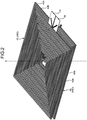
- FIG. 2 is a perspective view illustrating an exemplary configuration of a power transmission coil pattern 40C according to the embodiment.
- FIG. 3 is a plan view illustrating an exemplary configuration of the power transmission coil pattern 40C according to the embodiment.
- FIG. 4 is a rear view illustrating an exemplary configuration of the power transmission coil pattern 40C according to the embodiment.
- FIG. 5 is a partially enlarged view of FIG. 3 .
- the first coil pattern 42 is formed such that the first to sixth patterns 42a to 42f of the upper layer coil pattern 42A and the first to sixth patterns 42a to 42f of the lower layer coil pattern 42B each are stacked in the layers of the first base material 41. Then, the first coil pattern 42 connects the first to sixth patterns 42a to 42f of the upper layer coil pattern 42A and the first to sixth patterns 42a to 42f of the lower layer coil pattern 42B respectively.
- the first and second coil patterns are configured such that the first inner side pattern and the second outer side pattern are connected, and the first outer side pattern and the second inner side pattern are connected. Therefore, a proximity effect can be suppressed, and the power can be appropriately transferred in a contactless manner.
Landscapes
- Engineering & Computer Science (AREA)
- Power Engineering (AREA)
- Computer Networks & Wireless Communication (AREA)
- Signal Processing (AREA)
- Coils Or Transformers For Communication (AREA)
- Coils Of Transformers For General Uses (AREA)
Abstract
Description
- The present invention relates to a power transmission unit.
- In recent years, there is disclosed a power transmission device as a power transmission unit which transfers power in a contactless manner in Japanese Patent Application Laid-open No.
2016-92214 - By the way, the power transmission device described in Japanese Patent Application Laid-open No.
2016-92214 - Therefore, the invention has been made in view of the problem, and an object thereof is to provide a power transmission unit which can appropriately transfer power in a contactless manner.
- In order to solve the above mentioned problem and achieve the object, a power transmission unit according to one aspect of the present invention includes a substrate, the substrate being configured to include: a first layer that includes a first base material formed in a flat shape and a first coil pattern formed in the first base material in a spiral shape about an axis line; and a second layer that includes a second base material formed in a flat shape and a second coil pattern formed in the second base material in a spiral shape about the axis line, and is stacked in the first layer, wherein the first coil pattern includes a first inner side pattern, and a first outer side pattern provided on an outer side of the first inner side pattern, the second coil pattern includes a second inner side pattern, and a second outer side pattern provided on an outer side of the second inner side pattern, and the first coil pattern and the second coil pattern are configured such that the first inner side pattern and the second outer side pattern are connected, and the first outer side pattern and the second inner side pattern are connected, and transfer power to a counterpart power transmission coil pattern in a contactless manner.
- According to another aspect of the present invention, in the power transmission unit, it is preferable that the first coil pattern is configured such that the first inner side pattern and the first outer side pattern each are stacked plural times in each layer of the first base material, the first inner side patterns are connected to each other, and the first outer side patterns are connected to each other, and the second coil pattern is configured such that the second inner side pattern and the second outer side pattern each are stacked plural times in each layer of the second base material, the second inner side patterns are connected to each other, and the second outer side patterns are connected to each other.
- According to still another aspect of the present invention, in the power transmission unit, it is preferable that the first coil pattern and the second coil pattern are configured such that an end on a side near the axis line of the first inner side pattern and an end on a side near the axis line of the second outer side pattern are connected, and an end on a side near the axis line of the first outer side pattern and an end on a side near the axis line of the second inner side pattern are connected.
- The above and other objects, features, advantages and technical and industrial significance of this invention will be better understood by reading the following detailed description of presently preferred embodiments of the invention, when considered in connection with the accompanying drawings.
-
-
FIG. 1 is a cross-sectional view illustrating an exemplary configuration of a power transmission unit according to an embodiment; -
FIG. 2 is a perspective view illustrating an exemplary configuration of a power transmission coil pattern according to an embodiment; -
FIG. 3 is a plan view illustrating an exemplary configuration of the power transmission coil pattern according to an embodiment; -
FIG. 4 is a rear view illustrating an exemplary configuration of the power transmission coil pattern according to an embodiment; -
FIG. 5 is a partially enlarged view ofFIG. 3 ; -
FIG. 6 is a diagram illustrating a high-frequency resistance (skin effect) of the power transmission coil pattern according to an embodiment; -
FIG. 7A is a diagram illustrating a current density distribution of the power transmission coil pattern (one coil pattern) according to a comparative example; -
FIG. 7B is a diagram illustrating the current density distribution of the power transmission coil pattern (three coil patterns) according to an embodiment; -
FIG. 7C is a diagram illustrating the current density distribution of the power transmission coil pattern (six coil patterns) according to an embodiment; -
FIG. 8 is a diagram illustrating an increasing rate of the high-frequency resistance of the power transmission coil pattern according to an embodiment; -
FIG. 9 is a diagram illustrating the high-frequency resistance (proximity effect) of the power transmission coil pattern according to an embodiment; -
FIG. 10A is a diagram illustrating the current density distribution of the power transmission coil pattern according to a comparative example; and -
FIG. 10B is a diagram illustrating the current density distribution of the power transmission coil pattern according to an embodiment. - Modes (embodiments) for carrying out the invention will be described with reference to the drawings. The invention is not limited to the content described in the following embodiments. In addition, the components described herein can be easily conceived by a person skilled in the art, and actually the same components are included. Further, the configurations described herein may be approximately combined. In addition, various omissions, replacements, or changes may be performed within a scope not departing from the spirit of the invention.
- A
power transmission device 1 according to an embodiment will be described with reference to the drawings.FIG. 1 is a cross-sectional view illustrating an exemplary configuration of thepower transmission device 1 according to the embodiment.FIG. 2 is a perspective view illustrating an exemplary configuration of a powertransmission coil pattern 40C according to the embodiment.FIG. 3 is a plan view illustrating an exemplary configuration of the powertransmission coil pattern 40C according to the embodiment.FIG. 4 is a rear view illustrating an exemplary configuration of the powertransmission coil pattern 40C according to the embodiment.FIG. 5 is a partially enlarged view ofFIG. 3 . - The
power transmission device 1 according to the embodiment is to transmit power in a contactless manner. Thepower transmission device 1 includes a power transmittingunit 1A as a power transmission unit and apower receiving unit 1B as a power transmission unit as illustrated inFIG. 1 . The power transmittingunit 1A is disposed to face thepower receiving unit 1B, and transmits power in a contactless manner. Thepower receiving unit 1B is disposed to face the power transmittingunit 1A, and receives power in a contactless manner. The power transmittingunit 1A and thepower receiving unit 1B have equivalent configurations. Therefore, the following description will be given about the power transmittingunit 1A, and the details of the power receivingunit 1B will be omitted. - The power transmitting
unit 1A includes apower line 10, anelectronic component 20, aferrite 30, and amultilayered board 40 as a substrate as illustrated inFIG. 1 . Thepower line 10 is a conductive line through which current flows. One end of thepower line 10 is connected to the power supply unit (not illustrated) which supplies power, and the other end is connected to themultilayered board 40. The current supplied from the power supply unit flows in thepower line 10 to themultilayered board 40. Theelectronic component 20 is mounted in a mounting surface of themultilayered board 40, and performs an electrical processing. - The
ferrite 30 is a member containing a magnetic material, for example, a complex oxide of iron oxide and metal. Theferrite 30 is formed in a rectangular plate shape for example, and formed in the same size as the powertransmission coil pattern 40C (seeFIG. 2 ). Theferrite 30 is disposed to face the powertransmission coil pattern 40C in an axial direction along an axis line X of the powertransmission coil pattern 40C. Theferrite 30 passes a magnetic flux generated by the powertransmission coil pattern 40C to suppress loss in the magnetic flux. - The
multilayered board 40 contains variouselectronic components 20 mounted therein, and forms an electronic circuit which electrically connects the electronic components 20 (so-called printed circuit board). Themultilayered board 40 is configured to include afirst layer 40A and asecond layer 40B, and is multilayered with thefirst layer 40A and thesecond layer 40B. - The
first layer 40A includes afirst base material 41 and afirst coil pattern 42. Thefirst base material 41 is configured by an insulating material such as epoxy resin, glass epoxy resin, paper epoxy resin, or ceramic, and is formed in a flat shape (film shape). Thefirst base material 41 is formed with a conductor pattern such as thefirst coil pattern 42 using a conductive member such as a copper foil. - The
first coil pattern 42 is a conductor pattern formed in thefirst base material 41 using a conductive member such as a copper foil. Thefirst coil pattern 42 is formed in a spiral shape about the axis line X as illustrated inFIGS. 2 and3 , and is formed in a rectangular shape (square shape) when viewed from the axial direction. Thefirst coil pattern 42 is configured by two layers and includes, for example, an upperlayer coil pattern 42A and a lowerlayer coil pattern 42B. The upperlayer coil pattern 42A and the lowerlayer coil pattern 42B each are formed and stacked in the layers of thefirst base material 41. - The upper
layer coil pattern 42A is formed such that six coil patterns are formed in a spiral shape about the axis line X. The upperlayer coil pattern 42A is formed with, for example, first tosixth patterns 42a to 42f as six coil patterns as illustrated inFIG. 5 . Thefirst pattern 42a is a pattern located on the innermost side. Thesecond pattern 42b is a pattern located on the second inner side. Thethird pattern 42c is a pattern located on the third inner side. Thefourth pattern 42d is a pattern located on the fourth inner side (that is, the third outer side). Thefifth pattern 42e is a pattern located on the second outer side. Thesixth pattern 42f is a pattern located on the outermost side. With six coil patterns, the upperlayer coil pattern 42A is formed such that the first tothird patterns 42a to 42c are relatively located on the inner side, and the fourth tosixth patterns 42d to 42f are relatively located on the outer side. In other words, the first tothird patterns 42a to 42c correspond to a first inner side pattern, and the fourth tosixth patterns 42d to 42f correspond to a first outer side pattern. - The lower
layer coil pattern 42B is configured similarly to the upperlayer coil pattern 42A, and connected to the upperlayer coil pattern 42A. Specifically, the lowerlayer coil pattern 42B is formed such that six coil patterns are formed in a spiral shape about the axis line X. The lowerlayer coil pattern 42B is formed with the first tosixth patterns 42a to 42f as six coil patterns as illustrated inFIGS. 2 and5 similarly to the upperlayer coil pattern 42A. With six coil patterns, the lowerlayer coil pattern 42B is formed such that the first tothird patterns 42a to 42c are relatively located on the inner side, and the fourth tosixth patterns 42d to 42f are relatively located on the outer side. - The
first coil pattern 42 is formed such that the first tosixth patterns 42a to 42f of the upperlayer coil pattern 42A and the first tosixth patterns 42a to 42f of the lowerlayer coil pattern 42B each are stacked in the layers of thefirst base material 41. Then, thefirst coil pattern 42 connects the first tosixth patterns 42a to 42f of the upperlayer coil pattern 42A and the first tosixth patterns 42a to 42f of the lowerlayer coil pattern 42B respectively. Specifically, thefirst coil pattern 42 connects thefirst pattern 42a of the upperlayer coil pattern 42A and thefirst pattern 42a of the lowerlayer coil pattern 42B, thesecond pattern 42b of the upperlayer coil pattern 42A and thesecond pattern 42b of the lowerlayer coil pattern 42B, and thethird pattern 42c of the upperlayer coil pattern 42A and thethird pattern 42c of the lowerlayer coil pattern 42B. In addition, thefirst coil pattern 42 connects thefourth pattern 42d of the upperlayer coil pattern 42A and thefourth pattern 42d of the lowerlayer coil pattern 42B, thefifth pattern 42e of the upperlayer coil pattern 42A and thefifth pattern 42e of the lowerlayer coil pattern 42B, and thesixth pattern 42f of the upperlayer coil pattern 42A and thesixth pattern 42f of the lowerlayer coil pattern 42B. - Next, the
second layer 40B will be described. Thesecond layer 40B is configured equivalently to thefirst layer 40A. Specifically, thesecond layer 40B includes asecond base material 44 and asecond coil pattern 45. Thesecond base material 44 is configured by an insulating material such as epoxy resin, glass epoxy resin, paper epoxy resin, or ceramic, and is formed in a flat shape (film shape). Thesecond base material 44 is formed with a conductor pattern such as thesecond coil pattern 45 using a conductive member such as a copper foil. - The
second coil pattern 45 is a conductor pattern formed in thesecond base material 44 using a conductive member such as a copper foil. Thesecond coil pattern 45 is formed in a spiral shape about the axis line X as illustrated inFIGS. 2 and4 , and is formed in a rectangular shape (square shape) when viewed from the axial direction. Thesecond coil pattern 45 is configured by two layers and includes, for example, an upperlayer coil pattern 45A and a lowerlayer coil pattern 45B. The upperlayer coil pattern 45A and the lowerlayer coil pattern 45B each are formed and stacked in the layers of thesecond base material 44. - The upper
layer coil pattern 45A is formed such that six coil patterns are formed in a spiral shape about the axis line X. The upperlayer coil pattern 45A is formed with, for example, afirst pattern 45a to thesixth pattern 45f as six coil patterns as illustrated inFIG. 5 . Thefirst pattern 45a is a pattern located on the innermost side. Thesecond pattern 45b is a pattern located on the second inner side. Thethird pattern 45c is a pattern located on the third inner side. Thefourth pattern 45d is a pattern located on the fourth inner side (that is, the third outer side). Thefifth pattern 45e is a pattern located on the second outer side. Thesixth pattern 45f is a pattern located on the outermost side. With six coil patterns, the upperlayer coil pattern 45A is formed such that the first tothird patterns 45a to 45c are relatively located on the inner side, and the fourth tosixth patterns 45d to 45f are relatively located on the outer side. In other words, the first tothird patterns 45a to 45c correspond to a second inner side pattern, and the fourth tosixth patterns 45d to 45f correspond to a second outer side pattern. - The lower
layer coil pattern 45B is configured similarly to the upperlayer coil pattern 45A, and connected to the upperlayer coil pattern 45A. Specifically, the lowerlayer coil pattern 45B is formed such that six coil patterns are formed in a spiral shape about the axis line X. The lowerlayer coil pattern 45B is formed with the first tosixth patterns 45a to 45f as six coil patterns as illustrated inFIGS. 2 and5 similarly to the upperlayer coil pattern 45A. With six coil patterns, the lowerlayer coil pattern 45B is formed such that the first tothird patterns 45a to 45c are relatively located on the inner side, and the fourth tosixth patterns 45d to 45f are relatively located on the outer side. - The
second coil pattern 45 is formed such that the first tosixth patterns 45a to 45f of the upperlayer coil pattern 45A and the first tosixth patterns 45a to 45f of the lowerlayer coil pattern 45B each are stacked in the layers of thesecond base material 44. Then, thesecond coil pattern 45 connects the first tosixth patterns 45a to 45f of the upperlayer coil pattern 45A and the first tosixth patterns 45a to 45f of the lowerlayer coil pattern 45B respectively. Specifically, thesecond coil pattern 45 connects thefirst pattern 45a of the upperlayer coil pattern 45A and thefirst pattern 45a of the lowerlayer coil pattern 45B, thesecond pattern 45b of the upperlayer coil pattern 45A and thesecond pattern 45b of the lowerlayer coil pattern 45B, and thethird pattern 45c of the upperlayer coil pattern 45A and thethird pattern 45c of the lowerlayer coil pattern 45B. In addition, thefirst coil pattern 42 connects thefourth pattern 45d of the upperlayer coil pattern 45A and thefourth pattern 45d of the lowerlayer coil pattern 45B, thefifth pattern 45e of the upperlayer coil pattern 45A and thefifth pattern 45e of the lowerlayer coil pattern 45B, and thesixth pattern 45f of the upperlayer coil pattern 45A and thesixth pattern 45f of the lowerlayer coil pattern 45B. - Then, the first and
second coil patterns third patterns 42a to 42c on the inner side of thefirst coil pattern 42 are connected to the fourth tosixth patterns 45d to 45f on the outer side of thesecond coil pattern 45. The first andsecond coil patterns third patterns 42a to 42c are connected to ends 450d to 450f on a side near the axis line X of the fourth tosixth patterns 45d to 45f. - In addition, the first and
second coil patterns sixth patterns 42d to 42f on the outer side of thefirst coil pattern 42 are connected to the first tothird patterns 45a to 45c on the inner side of thesecond coil pattern 45. The first andsecond coil patterns sixth patterns 42d to 42f are connected to ends 450a to 450c on a side near the axis line X of the first tothird patterns 45a to 45c. - Specifically, the first and
second coil patterns end 420a of thefirst pattern 42a on the innermost side of thefirst coil pattern 42 is connected to theend 450f of thesixth pattern 45f on the outermost side of thesecond coil pattern 45, theend 420b of thesecond pattern 42b on the second inner side of thefirst coil pattern 42 is connected to theend 450e of thefifth pattern 45e on the second outer side of thesecond coil pattern 45, and theend 420c of thethird pattern 42c on the third inner side of thefirst coil pattern 42 is connected to theend 450d of thefourth pattern 45d on the third outer side of thesecond coil pattern 45. - In addition, the first and
second coil patterns sixth pattern 42f on the outermost side of thefirst coil pattern 42 is connected to the end 450a of thefirst pattern 45a on the innermost side of thesecond coil pattern 45, theend 420e of thefifth pattern 42e on the second outer side of thefirst coil pattern 42 is connected to theend 450b of thesecond pattern 45b on the second inner side of thesecond coil pattern 45, and theend 420d of thefourth pattern 42d on the third outer side of thefirst coil pattern 42 is connected to theend 450c of thethird pattern 45c on the third inner side of thesecond coil pattern 45. In addition, the end of thefirst coil pattern 42 on the opposite side to the axis line X is connected to a terminal 43. The end of thesecond coil pattern 45 on the opposite side to the axis line X is connected to a terminal 46. Then, the first andsecond coil patterns terminals power receiving unit 1B. - Next, a high-frequency resistance (skin effect) of the power
transmission coil pattern 40C will be described.FIG. 6 is a diagram illustrating the high-frequency resistance (skin effect) of the powertransmission coil pattern 40C according to the embodiment. InFIG. 6 , the vertical axis represents resistance (mΩ), and the horizontal axis represents frequency (Hz).FIG. 6 illustrates the high-frequency resistances in a case where the powertransmission coil pattern 40C is divided into one coil pattern, three coil patterns, and six coil patterns. Further, inFIG. 6 , results in a case where the number of coil patterns are changed are plotted, in which the connection of the coil patterns is similar to the related art and the outer side and the inner side are not connected. - In the power
transmission coil pattern 40C, the resistance of three coil patterns is lowest at around a frequency of 100 kHz as illustrated inFIG. 6 . In addition, in the powertransmission coil pattern 40C, the resistance of six coil patterns is lowest at a frequency exceeding 200 kHz. With this configuration, in the powertransmission coil pattern 40C, it can be seen that three coil patterns are desirably applied at around a frequency of 100 kHz, and six coil patterns are desirably applied in a case where the frequency exceeds 200 kHz. -
FIG. 7A is a diagram illustrating a current density distribution of a powertransmission coil pattern 40D (one coil pattern) according to a comparative example.FIG. 7B is a diagram illustrating the current density distribution of a powertransmission coil pattern 40E (three coil patterns) according to the embodiment.FIG. 7C is a diagram illustrating the current density distribution of the powertransmission coil pattern 40C (six coil patterns) according to the embodiment.FIGS. 7A to 7C illustrate the current density distribution at a frequency of 125 kHz. As illustrated inFIG. 7A , the current flowing to the powertransmission coil pattern 40D (one coil pattern) is concentrated on both sides of the coil pattern, and hardly flows to the center portion of the coil pattern. With this configuration, in the powertransmission coil pattern 40D, the effective conductor area where the current flows becomes relatively small, and the high-frequency resistance becomes relatively large. On the other hand, as illustrated inFIGS. 7B and 7C , the current flowing to the powertransmission coil pattern 40E (three coil patterns) and the powertransmission coil pattern 40C (six coil patterns) is not concentrated on one part of the coil pattern but flows evenly. With this configuration, the powertransmission coil patterns transmission coil patterns -
FIG. 8 is a diagram illustrating an increasing rate of the high-frequency resistance of the powertransmission coil pattern 40C according to the embodiment. InFIG. 8 , the vertical axis represents a rate (AC resistance/DC resistance) of an AC resistance to a DC resistance, and the horizontal axis represents frequency (Hz).FIG. 8 illustrates the AC resistance/DC resistance in a case where the powertransmission coil pattern 40C is one coil pattern, three coil patterns, six coil patterns, and a litz wire coil. - In the power
transmission coil pattern 40C, the AC resistances of one coil pattern and three coil patterns are increased when the frequency exceeds 20 kHz. In the powertransmission coil pattern 40C, the resistance of three coil patterns becomes larger than the litz wire coil when the frequency exceeds 60 kHz. In the powertransmission coil pattern 40C, the resistance of six coil patterns becomes larger than the resistance of the litz wire coil when the frequency exceeds 200 kHz even though the resistance of six coil patterns is lowest. With this configuration, it can be seen that, in the powertransmission coil pattern 40C, six coil patterns can suppress the skin effect at frequencies of 20 kHz to 200 kHz. - Next, the high-frequency resistance (proximity effect) of the power
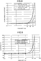
transmission coil pattern 40C will be described.FIG. 9 is a diagram illustrating the high-frequency resistance (proximity effect) of the powertransmission coil pattern 40C according to the embodiment. InFIG. 9 , the vertical axis represents resistance (mΩ), and the horizontal axis represents frequency (kHz).FIG. 9 illustrates the high-frequency resistance in powertransmission coil patterns FIGS. 10A and 10B in a case where the pattern is divided into three coil patterns. The powertransmission coil pattern 40F is a coil pattern in which theinner coil patterns 47a and theouter coil patterns 47c are connected. The powertransmission coil pattern 40G is a coil pattern which connects theinner coil pattern 47a and theouter coil pattern 47c. Further, the powertransmission coil patterns center coil patterns 47b. - It can be seen that he power
transmission coil pattern 40G has a high-frequency resistance smaller than the powertransmission coil pattern 40F as illustrated inFIG. 9 . It can be seen that the powertransmission coil pattern 40G has a high-frequency resistance smaller than the powertransmission coil pattern 40F by about 52 mQ, for example, in a case where the frequency is 100 kHz. In addition, it can be seen that the powertransmission coil pattern 40G has a high-frequency resistance smaller than the powertransmission coil pattern 40F by about 85 mΩ in a case where the frequency is 200 kHz. -
FIG. 10A is a diagram illustrating the current density distribution of the powertransmission coil pattern 40F according to a comparative example.FIG. 10B is a diagram illustrating the current density distribution of the powertransmission coil pattern 40G according to the embodiment. As illustrated inFIG. 10A , the current flowing to the powertransmission coil pattern 40F is concentrated on theinner coil pattern 47a, and hardly flows to theouter coil pattern 47c. With this configuration, in the powertransmission coil pattern 40F, the effective conductor area where the current flows becomes relatively small, and the high-frequency resistance becomes relatively large. On the other hand, as illustrated inFIG. 10B , the current flowing to the powertransmission coil pattern 40G is not concentrated on theinner coil pattern 47a, but flows evenly. With this configuration, the powertransmission coil pattern 40G can keep the effective conductor area where the current flows, and can suppress that the high-frequency resistance becomes large. As a result, the powertransmission coil pattern 40G can suppress the proximity effect. - As described above, the
power transmitting unit 1A according to the embodiment includes themultilayered board 40. Themultilayered board 40 is configured to include thefirst layer 40A and thesecond layer 40B. Thefirst layer 40A includes thefirst base material 41 formed in a flat shape and thefirst coil pattern 42 formed in thefirst base material 41 in a spiral shape about the axis line X. Thesecond layer 40B includes thesecond base material 44 formed in a flat shape and thesecond coil pattern 45 formed in thesecond base material 44 in a spiral shape about the axis line X, and is stacked in thefirst layer 40A. Thefirst coil pattern 42 includes the first tothird patterns 42a to 42c, and the fourth tosixth patterns 42d to 42f which are provided on the outer side of the first tothird patterns 42a to 42c. Thesecond coil pattern 45 includes the first tothird patterns 45a to 45c, and the fourth tosixth patterns 45d to 45f which are provided on the outer side of the first tothird patterns 45a to 45c. In the first andsecond coil patterns third patterns 42a to 42c on a first inner side and the fourth tosixth patterns 45d to 45f on a second inner side are connected. Further, the fourth tosixth patterns 42d to 42f on a first outer side and the first tothird patterns 45a to 45c on a second inner side are connected. Then, the first andsecond coil patterns power receiving unit 1B in a contactless manner. - With the configuration, the
power transmitting unit 1A is configured such that thefirst coil pattern 42 and thesecond coil pattern 45 each include a plurality of patterns, so that the skin effect can be suppressed. In addition, thepower transmitting unit 1A may be configured such that thefirst coil pattern 42 and thesecond coil pattern 45 are connected to increase the number of windings. Thepower transmitting unit 1A can reduce an influence of the magnetic flux by connecting the inner side and the outer side of the patterns, and the proximity effect can be suppressed. With the configuration, thepower transmitting unit 1A can suppress the high-frequency resistance, and a heating loss can be suppressed. As a result, thepower transmitting unit 1A can improve a power transmission efficiency, and can appropriately transfer power in a contactless manner. - In addition, in the
power transmitting unit 1A, a strand manufacturing, an enamel coating process, a twisting process, a coil winding process, a termination process, and a coil bonding process can be reduced compared to a coil formed with the litz wire. Therefore, it is possible to simplify a manufacturing process. In the case of the coil formed with the litz wire of the related art, a substrate for mounting theelectronic component 20 and a substrate for mounting a coil are prepared separately, and there is a need to connect these substrates. With this regard, in thepower transmitting unit 1A, theelectronic component 20 and the powertransmission coil pattern 40C can be formed in the samemultilayered board 40. It is possible to reduce the process of connecting themultilayered board 40. With the configuration, thepower transmitting unit 1A can suppress a manufacturing cost and an inspection cost. - In the
power transmitting unit 1A, thefirst coil pattern 42 is formed such that the first tothird patterns 42a to 42c and the fourth tosixth patterns 42d to 42f each are stacked plural times in each layer of thefirst base material 41, the first tothird patterns 42a to 42c are connected, and the fourth tosixth patterns 42d to 42f are connected. Thesecond coil pattern 45 is formed such that the first tothird patterns 45a to 45c and the fourth tosixth patterns 45d to 45f each are stacked plural times in each layer of thesecond base material 44, the first tothird patterns 45a to 45c are connected, and the fourth tosixth patterns 45d to 45f are connected. With the configuration, thepower transmitting unit 1A can increase a cross-sectional area of the powertransmission coil pattern 40C, and can increase the amount of transmitting power. - In the
power transmitting unit 1A, the first andsecond coil patterns ends 420a to 420c on a side near the axis line X of the first tothird patterns 42a to 42c on the first inner side are connected to theends 450d to 450f on a side near the axis line X of the fourth tosixth patterns 45d to 45f on the second outer side. In addition, the first andsecond coil patterns ends 420d to 420f on a side near the axis line X of the fourth tosixth patterns 42d to 42f on the first outer side are connected to the ends 450a to 450c on a side near the axis line X of the first tothird patterns 45a to 45c on the second inner side. With the configuration, thepower transmitting unit 1A can be configured such that thefirst coil pattern 42 and thesecond coil pattern 45 on a side near the axis line X of the powertransmission coil pattern 40C are connected. - Further, the above description has been described about an example where the first and
second coil patterns - In addition, the
first coil pattern 42 has been described to have two-layered configuration of the upperlayer coil pattern 42A and the lowerlayer coil pattern 42B, but the invention is not limited thereto. One-layered configuration or three-or-more-layered configurations may be employed. Similarly, thesecond coil pattern 45 has been described to have two-layered configuration of the upperlayer coil pattern 45A and the lowerlayer coil pattern 45B, but the invention is not limited thereto. One-layered configuration or three-or-more-layered configuration may be employed. - In the power transmission unit according to the embodiment, the first and second coil patterns are configured such that the first inner side pattern and the second outer side pattern are connected, and the first outer side pattern and the second inner side pattern are connected. Therefore, a proximity effect can be suppressed, and the power can be appropriately transferred in a contactless manner.
- Although the invention has been described with respect to specific embodiments for a complete and clear disclosure, the appended claims are not to be thus limited but are to be construed as embodying all modifications and alternative constructions that may occur to one skilled in the art that fairly fall within the basic teaching herein set forth.
Claims (3)
- A power transmission unit (1A, 1B), comprising:a substrate (40), the substrate (40) being configured to include:a first layer (40A) that includes a first base material (41) formed in a flat shape and a first coil pattern (42) formed in the first base material (41) in a spiral shape about an axis line (X); anda second layer (40B) that includes a second base material (44) formed in a flat shape and a second coil pattern (45) formed in the second base material (44) in a spiral shape about the axis line (X), and is stacked in the first layer (40A), whereinthe first coil pattern (42) includes a first inner side pattern (42a to 42c), and a first outer side pattern (42d to 42f) provided on an outer side of the first inner side pattern (42a to 42c),the second coil pattern (45) includes a second inner side pattern (45a to 45c), and a second outer side pattern (45d to 45f) provided on an outer side of the second inner side pattern (45a to 45c), andthe first coil pattern (42) and the second coil pattern (45) are configured such that the first inner side pattern (42a to 42c) and the second outer side pattern (45d to 45f) are connected, and the first outer side pattern (42d to 42f) and the second inner side pattern (45a to 45c) are connected, and transfer power to a counterpart power transmission coil pattern in a contactless manner.
- The power transmission unit (1A, 1B) according to claim 1, wherein
the first coil pattern (42) is configured such that the first inner side pattern (42a to 42c) and the first outer side pattern (42d to 42f) each are stacked plural times in each layer of the first base material (41), the first inner side patterns (42a to 42c) are connected to each other, and the first outer side patterns (42d to 42f) are connected to each other, and
the second coil pattern (45) is configured such that the second inner side pattern (45a to 45c) and the second outer side pattern (45d to 45f) each are stacked plural times in each layer of the second base material (44), the second inner side patterns (45a to 45c) are connected to each other, and the second outer side patterns (45d to 45f) are connected to each other. - The power transmission unit (1A, 1B) according to claim 1 or 2, wherein
the first coil pattern (42) and the second coil pattern (45) are configured such that an end (420a to 420c) on a side near the axis line (X) of the first inner side pattern (42a to 42c) and an end (450d to 450f) on a side near the axis line (X) of the second outer side pattern (45d to 45f) are connected, and an end (420d to 420f) on a side near the axis line (X) of the first outer side pattern (42d to 42f) and an end (450a to 450c) on a side near the axis line (X) of the second inner side pattern (45a to 45c) are connected.
Applications Claiming Priority (1)
| Application Number | Priority Date | Filing Date | Title |
|---|---|---|---|
| JP2018150242A JP2020027813A (en) | 2018-08-09 | 2018-08-09 | Power transmission unit |
Publications (2)
| Publication Number | Publication Date |
|---|---|
| EP3609051A1 true EP3609051A1 (en) | 2020-02-12 |
| EP3609051B1 EP3609051B1 (en) | 2020-11-04 |
Family
ID=67551236
Family Applications (1)
| Application Number | Title | Priority Date | Filing Date |
|---|---|---|---|
| EP19190430.9A Active EP3609051B1 (en) | 2018-08-09 | 2019-08-07 | Power transmission unit |
Country Status (4)
| Country | Link |
|---|---|
| US (1) | US10951067B2 (en) |
| EP (1) | EP3609051B1 (en) |
| JP (1) | JP2020027813A (en) |
| CN (1) | CN110828138B (en) |
Cited By (1)
| Publication number | Priority date | Publication date | Assignee | Title |
|---|---|---|---|---|
| GB2590331B (en) * | 2018-09-12 | 2022-11-02 | Multi Fineline Electronix Inc | Balanced, symmetrical coil |
Families Citing this family (3)
| Publication number | Priority date | Publication date | Assignee | Title |
|---|---|---|---|---|
| CN113012909A (en) * | 2021-03-01 | 2021-06-22 | 安徽安努奇科技有限公司 | Inductor |
| EP4356406A4 (en) | 2021-06-16 | 2025-04-16 | Resonant Link, Inc. | HIGHLY EFFICIENT WIRELESS POWER TRANSMISSION COILS |
| JP7819569B2 (en) * | 2022-04-27 | 2026-02-25 | 株式会社デンソー | Coil Device |
Citations (4)
| Publication number | Priority date | Publication date | Assignee | Title |
|---|---|---|---|---|
| US20110050380A1 (en) * | 2009-08-25 | 2011-03-03 | Sanken Electric Co., Ltd. | Coil apparatus |
| WO2012039045A1 (en) * | 2010-09-22 | 2012-03-29 | パイオニア株式会社 | Contactless power transmission coil |
| JP2016092214A (en) | 2014-11-05 | 2016-05-23 | トヨタ自動車株式会社 | Coil unit |
| WO2018222669A1 (en) * | 2017-05-30 | 2018-12-06 | Momentum Dynamics Corporation | Wireless power transfer thin profile coil assembly |
Family Cites Families (13)
| Publication number | Priority date | Publication date | Assignee | Title |
|---|---|---|---|---|
| JPH05128324A (en) * | 1991-11-07 | 1993-05-25 | Mitsubishi Electric Corp | Non-contact card, terminal machine for non-contact card, and non-contact transmission system |
| JPH0819985A (en) | 1994-07-04 | 1996-01-23 | Mitsubishi Electric Corp | Robot equipment |
| FI971180L (en) * | 1997-03-20 | 1998-12-23 | Micronas Oy | Stripe-line reel |
| JP2003043229A (en) | 2001-07-26 | 2003-02-13 | Furukawa Electric Co Ltd:The | Movable mirror device |
| CN101523693B (en) * | 2006-08-04 | 2012-05-23 | Sk化学株式会社 | Induction coil for cordless energy charging and data transfer |
| US7973635B2 (en) * | 2007-09-28 | 2011-07-05 | Access Business Group International Llc | Printed circuit board coil |
| JP4752879B2 (en) * | 2008-07-04 | 2011-08-17 | パナソニック電工株式会社 | Planar coil |
| CN102087909A (en) * | 2009-12-08 | 2011-06-08 | 上海华虹Nec电子有限公司 | Multi-path laminated inductor with inner path and outer path current compensation function |
| US9413196B2 (en) * | 2012-04-09 | 2016-08-09 | Toyota Motor Engineering & Manufacturing North America, Inc. | Wireless power transfer |
| CN102883525B (en) * | 2012-09-25 | 2015-06-10 | 清华大学 | Double-layered snail-shaped PCB coil for wireless energy transfer and design method thereof |
| JP6306288B2 (en) * | 2013-05-13 | 2018-04-04 | 日東電工株式会社 | Coil printed wiring board, power receiving module, battery unit and power receiving communication module |
| WO2016199516A1 (en) * | 2015-06-11 | 2016-12-15 | 株式会社村田製作所 | Coil-incorporating multilayer substrate and method for manufacturing same |
| JP2017168472A (en) * | 2016-03-14 | 2017-09-21 | 株式会社村田製作所 | Multilayer board |
-
2018
- 2018-08-09 JP JP2018150242A patent/JP2020027813A/en active Pending
-
2019
- 2019-07-18 US US16/515,773 patent/US10951067B2/en active Active
- 2019-08-07 EP EP19190430.9A patent/EP3609051B1/en active Active
- 2019-08-08 CN CN201910729829.8A patent/CN110828138B/en active Active
Patent Citations (4)
| Publication number | Priority date | Publication date | Assignee | Title |
|---|---|---|---|---|
| US20110050380A1 (en) * | 2009-08-25 | 2011-03-03 | Sanken Electric Co., Ltd. | Coil apparatus |
| WO2012039045A1 (en) * | 2010-09-22 | 2012-03-29 | パイオニア株式会社 | Contactless power transmission coil |
| JP2016092214A (en) | 2014-11-05 | 2016-05-23 | トヨタ自動車株式会社 | Coil unit |
| WO2018222669A1 (en) * | 2017-05-30 | 2018-12-06 | Momentum Dynamics Corporation | Wireless power transfer thin profile coil assembly |
Cited By (2)
| Publication number | Priority date | Publication date | Assignee | Title |
|---|---|---|---|---|
| GB2590331B (en) * | 2018-09-12 | 2022-11-02 | Multi Fineline Electronix Inc | Balanced, symmetrical coil |
| US11798728B2 (en) | 2018-09-12 | 2023-10-24 | DSBJ Pte. Ltd. | Balanced, symmetrical coil |
Also Published As
| Publication number | Publication date |
|---|---|
| EP3609051B1 (en) | 2020-11-04 |
| CN110828138B (en) | 2022-09-30 |
| US10951067B2 (en) | 2021-03-16 |
| CN110828138A (en) | 2020-02-21 |
| US20200052528A1 (en) | 2020-02-13 |
| JP2020027813A (en) | 2020-02-20 |
Similar Documents
| Publication | Publication Date | Title |
|---|---|---|
| EP3609051B1 (en) | Power transmission unit | |
| CN103915903B (en) | Be used for the coil of wireless charging and use the wireless charging device of this coil | |
| KR101339486B1 (en) | Thin film coil and electronic device having the same | |
| KR101452093B1 (en) | Thin film coil, shield part including the same, and contactless power transmission device having the shield part | |
| RU2481662C2 (en) | Flat coil | |
| KR101448024B1 (en) | Contactless power transmission system and transmission coil for contactless power transmission | |
| JPWO2004055841A1 (en) | Multiple choke coil and electronic device using the same | |
| CN106537532A (en) | Printed wiring board, antenna, and wireless power-feeding device | |
| CN110957117B (en) | Power transmission unit | |
| US9984804B2 (en) | Coil component | |
| WO2019009269A1 (en) | Flexible printed wiring board | |
| WO2022007706A1 (en) | Winding assembly, on-board charger, and vehicle | |
| JPH11176676A (en) | Small contactless transmission device | |
| JP2016051853A (en) | Power reception device and coil unit for the same | |
| CN205389009U (en) | SMD NFC antenna of zigzag and antenna system | |
| KR101546718B1 (en) | Thin film coil, case assembly, non-contact power receiving device, and electronic device having the same | |
| KR101546720B1 (en) | Thin film coil, case assembly, non-contact power receiving device, and electronic device having the same | |
| CN212849958U (en) | Wireless charging coil and wireless charging device | |
| JP6597431B2 (en) | Antenna device and communication device | |
| KR101546719B1 (en) | Non-contact power receiving device, case assembly, and electronic device having the same | |
| CN210896936U (en) | Inductance element and electronic equipment | |
| KR101973453B1 (en) | Thin film coil, wireless power receiving device, electronic apparatus, and case assembly | |
| EP4235712A1 (en) | Magnetic element and image output device comprising same | |
| KR20160107141A (en) | Thin film coil, wireless power receiving device, electronic apparatus, and case assembly | |
| KR101581695B1 (en) | Coil substrate |
Legal Events
| Date | Code | Title | Description |
|---|---|---|---|
| PUAI | Public reference made under article 153(3) epc to a published international application that has entered the european phase |
Free format text: ORIGINAL CODE: 0009012 |
|
| STAA | Information on the status of an ep patent application or granted ep patent |
Free format text: STATUS: REQUEST FOR EXAMINATION WAS MADE |
|
| 17P | Request for examination filed |
Effective date: 20190807 |
|
| AK | Designated contracting states |
Kind code of ref document: A1 Designated state(s): AL AT BE BG CH CY CZ DE DK EE ES FI FR GB GR HR HU IE IS IT LI LT LU LV MC MK MT NL NO PL PT RO RS SE SI SK SM TR |
|
| AX | Request for extension of the european patent |
Extension state: BA ME |
|
| RBV | Designated contracting states (corrected) |
Designated state(s): AL AT BE BG CH CY CZ DE DK EE ES FI FR GB GR HR HU IE IS IT LI LT LU LV MC MK MT NL NO PL PT RO RS SE SI SK SM TR |
|
| GRAP | Despatch of communication of intention to grant a patent |
Free format text: ORIGINAL CODE: EPIDOSNIGR1 |
|
| STAA | Information on the status of an ep patent application or granted ep patent |
Free format text: STATUS: GRANT OF PATENT IS INTENDED |
|
| RIC1 | Information provided on ipc code assigned before grant |
Ipc: H01F 27/28 20060101ALI20200706BHEP Ipc: H04B 5/00 20060101ALI20200706BHEP Ipc: H02J 50/00 20160101ALI20200706BHEP Ipc: H01F 38/14 20060101ALI20200706BHEP Ipc: H02J 50/12 20160101AFI20200706BHEP |
|
| INTG | Intention to grant announced |
Effective date: 20200805 |
|
| GRAS | Grant fee paid |
Free format text: ORIGINAL CODE: EPIDOSNIGR3 |
|
| GRAA | (expected) grant |
Free format text: ORIGINAL CODE: 0009210 |
|
| STAA | Information on the status of an ep patent application or granted ep patent |
Free format text: STATUS: THE PATENT HAS BEEN GRANTED |
|
| AK | Designated contracting states |
Kind code of ref document: B1 Designated state(s): AL AT BE BG CH CY CZ DE DK EE ES FI FR GB GR HR HU IE IS IT LI LT LU LV MC MK MT NL NO PL PT RO RS SE SI SK SM TR |
|
| REG | Reference to a national code |
Ref country code: GB Ref legal event code: FG4D |
|
| REG | Reference to a national code |
Ref country code: CH Ref legal event code: EP |
|
| REG | Reference to a national code |
Ref country code: AT Ref legal event code: REF Ref document number: 1332094 Country of ref document: AT Kind code of ref document: T Effective date: 20201115 |
|
| REG | Reference to a national code |
Ref country code: IE Ref legal event code: FG4D |
|
| REG | Reference to a national code |
Ref country code: DE Ref legal event code: R096 Ref document number: 602019001198 Country of ref document: DE |
|
| REG | Reference to a national code |
Ref country code: NL Ref legal event code: MP Effective date: 20201104 |
|
| REG | Reference to a national code |
Ref country code: AT Ref legal event code: MK05 Ref document number: 1332094 Country of ref document: AT Kind code of ref document: T Effective date: 20201104 |
|
| PG25 | Lapsed in a contracting state [announced via postgrant information from national office to epo] |
Ref country code: PT Free format text: LAPSE BECAUSE OF FAILURE TO SUBMIT A TRANSLATION OF THE DESCRIPTION OR TO PAY THE FEE WITHIN THE PRESCRIBED TIME-LIMIT Effective date: 20210304 Ref country code: RS Free format text: LAPSE BECAUSE OF FAILURE TO SUBMIT A TRANSLATION OF THE DESCRIPTION OR TO PAY THE FEE WITHIN THE PRESCRIBED TIME-LIMIT Effective date: 20201104 Ref country code: FI Free format text: LAPSE BECAUSE OF FAILURE TO SUBMIT A TRANSLATION OF THE DESCRIPTION OR TO PAY THE FEE WITHIN THE PRESCRIBED TIME-LIMIT Effective date: 20201104 Ref country code: NO Free format text: LAPSE BECAUSE OF FAILURE TO SUBMIT A TRANSLATION OF THE DESCRIPTION OR TO PAY THE FEE WITHIN THE PRESCRIBED TIME-LIMIT Effective date: 20210204 Ref country code: GR Free format text: LAPSE BECAUSE OF FAILURE TO SUBMIT A TRANSLATION OF THE DESCRIPTION OR TO PAY THE FEE WITHIN THE PRESCRIBED TIME-LIMIT Effective date: 20210205 |
|
| PG25 | Lapsed in a contracting state [announced via postgrant information from national office to epo] |
Ref country code: AT Free format text: LAPSE BECAUSE OF FAILURE TO SUBMIT A TRANSLATION OF THE DESCRIPTION OR TO PAY THE FEE WITHIN THE PRESCRIBED TIME-LIMIT Effective date: 20201104 Ref country code: ES Free format text: LAPSE BECAUSE OF FAILURE TO SUBMIT A TRANSLATION OF THE DESCRIPTION OR TO PAY THE FEE WITHIN THE PRESCRIBED TIME-LIMIT Effective date: 20201104 Ref country code: BG Free format text: LAPSE BECAUSE OF FAILURE TO SUBMIT A TRANSLATION OF THE DESCRIPTION OR TO PAY THE FEE WITHIN THE PRESCRIBED TIME-LIMIT Effective date: 20210204 Ref country code: SE Free format text: LAPSE BECAUSE OF FAILURE TO SUBMIT A TRANSLATION OF THE DESCRIPTION OR TO PAY THE FEE WITHIN THE PRESCRIBED TIME-LIMIT Effective date: 20201104 Ref country code: IS Free format text: LAPSE BECAUSE OF FAILURE TO SUBMIT A TRANSLATION OF THE DESCRIPTION OR TO PAY THE FEE WITHIN THE PRESCRIBED TIME-LIMIT Effective date: 20210304 Ref country code: LV Free format text: LAPSE BECAUSE OF FAILURE TO SUBMIT A TRANSLATION OF THE DESCRIPTION OR TO PAY THE FEE WITHIN THE PRESCRIBED TIME-LIMIT Effective date: 20201104 Ref country code: PL Free format text: LAPSE BECAUSE OF FAILURE TO SUBMIT A TRANSLATION OF THE DESCRIPTION OR TO PAY THE FEE WITHIN THE PRESCRIBED TIME-LIMIT Effective date: 20201104 |
|
| REG | Reference to a national code |
Ref country code: LT Ref legal event code: MG9D |
|
| PG25 | Lapsed in a contracting state [announced via postgrant information from national office to epo] |
Ref country code: HR Free format text: LAPSE BECAUSE OF FAILURE TO SUBMIT A TRANSLATION OF THE DESCRIPTION OR TO PAY THE FEE WITHIN THE PRESCRIBED TIME-LIMIT Effective date: 20201104 |
|
| PG25 | Lapsed in a contracting state [announced via postgrant information from national office to epo] |
Ref country code: CZ Free format text: LAPSE BECAUSE OF FAILURE TO SUBMIT A TRANSLATION OF THE DESCRIPTION OR TO PAY THE FEE WITHIN THE PRESCRIBED TIME-LIMIT Effective date: 20201104 Ref country code: SM Free format text: LAPSE BECAUSE OF FAILURE TO SUBMIT A TRANSLATION OF THE DESCRIPTION OR TO PAY THE FEE WITHIN THE PRESCRIBED TIME-LIMIT Effective date: 20201104 Ref country code: SK Free format text: LAPSE BECAUSE OF FAILURE TO SUBMIT A TRANSLATION OF THE DESCRIPTION OR TO PAY THE FEE WITHIN THE PRESCRIBED TIME-LIMIT Effective date: 20201104 Ref country code: EE Free format text: LAPSE BECAUSE OF FAILURE TO SUBMIT A TRANSLATION OF THE DESCRIPTION OR TO PAY THE FEE WITHIN THE PRESCRIBED TIME-LIMIT Effective date: 20201104 Ref country code: LT Free format text: LAPSE BECAUSE OF FAILURE TO SUBMIT A TRANSLATION OF THE DESCRIPTION OR TO PAY THE FEE WITHIN THE PRESCRIBED TIME-LIMIT Effective date: 20201104 Ref country code: RO Free format text: LAPSE BECAUSE OF FAILURE TO SUBMIT A TRANSLATION OF THE DESCRIPTION OR TO PAY THE FEE WITHIN THE PRESCRIBED TIME-LIMIT Effective date: 20201104 |
|
| REG | Reference to a national code |
Ref country code: DE Ref legal event code: R097 Ref document number: 602019001198 Country of ref document: DE |
|
| PG25 | Lapsed in a contracting state [announced via postgrant information from national office to epo] |
Ref country code: DK Free format text: LAPSE BECAUSE OF FAILURE TO SUBMIT A TRANSLATION OF THE DESCRIPTION OR TO PAY THE FEE WITHIN THE PRESCRIBED TIME-LIMIT Effective date: 20201104 |
|
| PLBE | No opposition filed within time limit |
Free format text: ORIGINAL CODE: 0009261 |
|
| STAA | Information on the status of an ep patent application or granted ep patent |
Free format text: STATUS: NO OPPOSITION FILED WITHIN TIME LIMIT |
|
| 26N | No opposition filed |
Effective date: 20210805 |
|
| PG25 | Lapsed in a contracting state [announced via postgrant information from national office to epo] |
Ref country code: IT Free format text: LAPSE BECAUSE OF FAILURE TO SUBMIT A TRANSLATION OF THE DESCRIPTION OR TO PAY THE FEE WITHIN THE PRESCRIBED TIME-LIMIT Effective date: 20201104 Ref country code: AL Free format text: LAPSE BECAUSE OF FAILURE TO SUBMIT A TRANSLATION OF THE DESCRIPTION OR TO PAY THE FEE WITHIN THE PRESCRIBED TIME-LIMIT Effective date: 20201104 Ref country code: NL Free format text: LAPSE BECAUSE OF FAILURE TO SUBMIT A TRANSLATION OF THE DESCRIPTION OR TO PAY THE FEE WITHIN THE PRESCRIBED TIME-LIMIT Effective date: 20201104 |
|
| PG25 | Lapsed in a contracting state [announced via postgrant information from national office to epo] |
Ref country code: SI Free format text: LAPSE BECAUSE OF FAILURE TO SUBMIT A TRANSLATION OF THE DESCRIPTION OR TO PAY THE FEE WITHIN THE PRESCRIBED TIME-LIMIT Effective date: 20201104 |
|
| PG25 | Lapsed in a contracting state [announced via postgrant information from national office to epo] |
Ref country code: MC Free format text: LAPSE BECAUSE OF FAILURE TO SUBMIT A TRANSLATION OF THE DESCRIPTION OR TO PAY THE FEE WITHIN THE PRESCRIBED TIME-LIMIT Effective date: 20201104 |
|
| REG | Reference to a national code |
Ref country code: BE Ref legal event code: MM Effective date: 20210831 |
|
| PG25 | Lapsed in a contracting state [announced via postgrant information from national office to epo] |
Ref country code: IS Free format text: LAPSE BECAUSE OF FAILURE TO SUBMIT A TRANSLATION OF THE DESCRIPTION OR TO PAY THE FEE WITHIN THE PRESCRIBED TIME-LIMIT Effective date: 20210304 Ref country code: LU Free format text: LAPSE BECAUSE OF NON-PAYMENT OF DUE FEES Effective date: 20210807 |
|
| PG25 | Lapsed in a contracting state [announced via postgrant information from national office to epo] |
Ref country code: IE Free format text: LAPSE BECAUSE OF NON-PAYMENT OF DUE FEES Effective date: 20210807 Ref country code: FR Free format text: LAPSE BECAUSE OF NON-PAYMENT OF DUE FEES Effective date: 20210831 Ref country code: BE Free format text: LAPSE BECAUSE OF NON-PAYMENT OF DUE FEES Effective date: 20210831 |
|
| REG | Reference to a national code |
Ref country code: CH Ref legal event code: PL |
|
| PG25 | Lapsed in a contracting state [announced via postgrant information from national office to epo] |
Ref country code: LI Free format text: LAPSE BECAUSE OF NON-PAYMENT OF DUE FEES Effective date: 20220831 Ref country code: CH Free format text: LAPSE BECAUSE OF NON-PAYMENT OF DUE FEES Effective date: 20220831 |
|
| PG25 | Lapsed in a contracting state [announced via postgrant information from national office to epo] |
Ref country code: CY Free format text: LAPSE BECAUSE OF FAILURE TO SUBMIT A TRANSLATION OF THE DESCRIPTION OR TO PAY THE FEE WITHIN THE PRESCRIBED TIME-LIMIT Effective date: 20201104 |
|
| PG25 | Lapsed in a contracting state [announced via postgrant information from national office to epo] |
Ref country code: HU Free format text: LAPSE BECAUSE OF FAILURE TO SUBMIT A TRANSLATION OF THE DESCRIPTION OR TO PAY THE FEE WITHIN THE PRESCRIBED TIME-LIMIT; INVALID AB INITIO Effective date: 20190807 |
|
| GBPC | Gb: european patent ceased through non-payment of renewal fee |
Effective date: 20230807 |
|
| PG25 | Lapsed in a contracting state [announced via postgrant information from national office to epo] |
Ref country code: MK Free format text: LAPSE BECAUSE OF FAILURE TO SUBMIT A TRANSLATION OF THE DESCRIPTION OR TO PAY THE FEE WITHIN THE PRESCRIBED TIME-LIMIT Effective date: 20201104 |
|
| PG25 | Lapsed in a contracting state [announced via postgrant information from national office to epo] |
Ref country code: GB Free format text: LAPSE BECAUSE OF NON-PAYMENT OF DUE FEES Effective date: 20230807 |
|
| PG25 | Lapsed in a contracting state [announced via postgrant information from national office to epo] |
Ref country code: GB Free format text: LAPSE BECAUSE OF NON-PAYMENT OF DUE FEES Effective date: 20230807 |
|
| PG25 | Lapsed in a contracting state [announced via postgrant information from national office to epo] |
Ref country code: MT Free format text: LAPSE BECAUSE OF FAILURE TO SUBMIT A TRANSLATION OF THE DESCRIPTION OR TO PAY THE FEE WITHIN THE PRESCRIBED TIME-LIMIT Effective date: 20201104 |
|
| PGFP | Annual fee paid to national office [announced via postgrant information from national office to epo] |
Ref country code: DE Payment date: 20250702 Year of fee payment: 7 |
|
| PG25 | Lapsed in a contracting state [announced via postgrant information from national office to epo] |
Ref country code: TR Free format text: LAPSE BECAUSE OF FAILURE TO SUBMIT A TRANSLATION OF THE DESCRIPTION OR TO PAY THE FEE WITHIN THE PRESCRIBED TIME-LIMIT Effective date: 20201104 |