EP3608967A1 - Oxygen inserted si-layers in vertical trench power devices - Google Patents
Oxygen inserted si-layers in vertical trench power devices Download PDFInfo
- Publication number
- EP3608967A1 EP3608967A1 EP19189117.5A EP19189117A EP3608967A1 EP 3608967 A1 EP3608967 A1 EP 3608967A1 EP 19189117 A EP19189117 A EP 19189117A EP 3608967 A1 EP3608967 A1 EP 3608967A1
- Authority
- EP
- European Patent Office
- Prior art keywords
- gate trench
- trench
- gate
- sidewall
- forming
- Prior art date
- Legal status (The legal status is an assumption and is not a legal conclusion. Google has not performed a legal analysis and makes no representation as to the accuracy of the status listed.)
- Granted
Links
Images













Classifications
-
- H—ELECTRICITY
- H10—SEMICONDUCTOR DEVICES; ELECTRIC SOLID-STATE DEVICES NOT OTHERWISE PROVIDED FOR
- H10D—INORGANIC ELECTRIC SEMICONDUCTOR DEVICES
- H10D64/00—Electrodes of devices having potential barriers
- H10D64/60—Electrodes characterised by their materials
- H10D64/66—Electrodes having a conductor capacitively coupled to a semiconductor by an insulator, e.g. MIS electrodes
- H10D64/661—Electrodes having a conductor capacitively coupled to a semiconductor by an insulator, e.g. MIS electrodes the conductor comprising a layer of silicon contacting the insulator, e.g. polysilicon having vertical doping variation
- H10D64/662—Electrodes having a conductor capacitively coupled to a semiconductor by an insulator, e.g. MIS electrodes the conductor comprising a layer of silicon contacting the insulator, e.g. polysilicon having vertical doping variation the conductor further comprising additional layers, e.g. multiple silicon layers having different crystal structures
- H10D64/664—Electrodes having a conductor capacitively coupled to a semiconductor by an insulator, e.g. MIS electrodes the conductor comprising a layer of silicon contacting the insulator, e.g. polysilicon having vertical doping variation the conductor further comprising additional layers, e.g. multiple silicon layers having different crystal structures the additional layers comprising a barrier layer between the layer of silicon and an upper metal or metal silicide layer
-
- H—ELECTRICITY
- H10—SEMICONDUCTOR DEVICES; ELECTRIC SOLID-STATE DEVICES NOT OTHERWISE PROVIDED FOR
- H10D—INORGANIC ELECTRIC SEMICONDUCTOR DEVICES
- H10D30/00—Field-effect transistors [FET]
- H10D30/60—Insulated-gate field-effect transistors [IGFET]
- H10D30/64—Double-diffused metal-oxide semiconductor [DMOS] FETs
- H10D30/66—Vertical DMOS [VDMOS] FETs
- H10D30/668—Vertical DMOS [VDMOS] FETs having trench gate electrodes, e.g. UMOS transistors
-
- H—ELECTRICITY
- H10—SEMICONDUCTOR DEVICES; ELECTRIC SOLID-STATE DEVICES NOT OTHERWISE PROVIDED FOR
- H10D—INORGANIC ELECTRIC SEMICONDUCTOR DEVICES
- H10D30/00—Field-effect transistors [FET]
- H10D30/60—Insulated-gate field-effect transistors [IGFET]
- H10D30/63—Vertical IGFETs
- H10D30/635—Vertical IGFETs having no inversion channels, e.g. vertical accumulation channel FETs [ACCUFET] or normally-on vertical IGFETs
-
- H—ELECTRICITY
- H10—SEMICONDUCTOR DEVICES; ELECTRIC SOLID-STATE DEVICES NOT OTHERWISE PROVIDED FOR
- H10D—INORGANIC ELECTRIC SEMICONDUCTOR DEVICES
- H10D12/00—Bipolar devices controlled by the field effect, e.g. insulated-gate bipolar transistors [IGBT]
- H10D12/01—Manufacture or treatment
- H10D12/031—Manufacture or treatment of IGBTs
- H10D12/032—Manufacture or treatment of IGBTs of vertical IGBTs
- H10D12/038—Manufacture or treatment of IGBTs of vertical IGBTs having a recessed gate, e.g. trench-gate IGBTs
-
- H—ELECTRICITY
- H10—SEMICONDUCTOR DEVICES; ELECTRIC SOLID-STATE DEVICES NOT OTHERWISE PROVIDED FOR
- H10D—INORGANIC ELECTRIC SEMICONDUCTOR DEVICES
- H10D12/00—Bipolar devices controlled by the field effect, e.g. insulated-gate bipolar transistors [IGBT]
- H10D12/411—Insulated-gate bipolar transistors [IGBT]
- H10D12/441—Vertical IGBTs
- H10D12/461—Vertical IGBTs having non-planar surfaces, e.g. having trenches, recesses or pillars in the surfaces of the emitter, base or collector regions
- H10D12/481—Vertical IGBTs having non-planar surfaces, e.g. having trenches, recesses or pillars in the surfaces of the emitter, base or collector regions having gate structures on slanted surfaces, on vertical surfaces, or in grooves, e.g. trench gate IGBTs
-
- H—ELECTRICITY
- H10—SEMICONDUCTOR DEVICES; ELECTRIC SOLID-STATE DEVICES NOT OTHERWISE PROVIDED FOR
- H10D—INORGANIC ELECTRIC SEMICONDUCTOR DEVICES
- H10D30/00—Field-effect transistors [FET]
- H10D30/01—Manufacture or treatment
- H10D30/021—Manufacture or treatment of FETs having insulated gates [IGFET]
- H10D30/025—Manufacture or treatment of FETs having insulated gates [IGFET] of vertical IGFETs
-
- H—ELECTRICITY
- H10—SEMICONDUCTOR DEVICES; ELECTRIC SOLID-STATE DEVICES NOT OTHERWISE PROVIDED FOR
- H10D—INORGANIC ELECTRIC SEMICONDUCTOR DEVICES
- H10D30/00—Field-effect transistors [FET]
- H10D30/01—Manufacture or treatment
- H10D30/021—Manufacture or treatment of FETs having insulated gates [IGFET]
- H10D30/028—Manufacture or treatment of FETs having insulated gates [IGFET] of double-diffused metal oxide semiconductor [DMOS] FETs
- H10D30/0291—Manufacture or treatment of FETs having insulated gates [IGFET] of double-diffused metal oxide semiconductor [DMOS] FETs of vertical DMOS [VDMOS] FETs
- H10D30/0297—Manufacture or treatment of FETs having insulated gates [IGFET] of double-diffused metal oxide semiconductor [DMOS] FETs of vertical DMOS [VDMOS] FETs using recessing of the gate electrodes, e.g. to form trench gate electrodes
-
- H—ELECTRICITY
- H10—SEMICONDUCTOR DEVICES; ELECTRIC SOLID-STATE DEVICES NOT OTHERWISE PROVIDED FOR
- H10D—INORGANIC ELECTRIC SEMICONDUCTOR DEVICES
- H10D62/00—Semiconductor bodies, or regions thereof, of devices having potential barriers
- H10D62/10—Shapes, relative sizes or dispositions of the regions of the semiconductor bodies; Shapes of the semiconductor bodies
- H10D62/13—Semiconductor regions connected to electrodes carrying current to be rectified, amplified or switched, e.g. source or drain regions
- H10D62/149—Source or drain regions of field-effect devices
- H10D62/151—Source or drain regions of field-effect devices of IGFETs
- H10D62/152—Source regions of DMOS transistors
-
- H—ELECTRICITY
- H10—SEMICONDUCTOR DEVICES; ELECTRIC SOLID-STATE DEVICES NOT OTHERWISE PROVIDED FOR
- H10D—INORGANIC ELECTRIC SEMICONDUCTOR DEVICES
- H10D62/00—Semiconductor bodies, or regions thereof, of devices having potential barriers
- H10D62/10—Shapes, relative sizes or dispositions of the regions of the semiconductor bodies; Shapes of the semiconductor bodies
- H10D62/17—Semiconductor regions connected to electrodes not carrying current to be rectified, amplified or switched, e.g. channel regions
- H10D62/213—Channel regions of field-effect devices
- H10D62/221—Channel regions of field-effect devices of FETs
- H10D62/235—Channel regions of field-effect devices of FETs of IGFETs
-
- H—ELECTRICITY
- H10—SEMICONDUCTOR DEVICES; ELECTRIC SOLID-STATE DEVICES NOT OTHERWISE PROVIDED FOR
- H10D—INORGANIC ELECTRIC SEMICONDUCTOR DEVICES
- H10D62/00—Semiconductor bodies, or regions thereof, of devices having potential barriers
- H10D62/10—Shapes, relative sizes or dispositions of the regions of the semiconductor bodies; Shapes of the semiconductor bodies
- H10D62/17—Semiconductor regions connected to electrodes not carrying current to be rectified, amplified or switched, e.g. channel regions
- H10D62/393—Body regions of DMOS transistors or IGBTs
-
- H—ELECTRICITY
- H10—SEMICONDUCTOR DEVICES; ELECTRIC SOLID-STATE DEVICES NOT OTHERWISE PROVIDED FOR
- H10D—INORGANIC ELECTRIC SEMICONDUCTOR DEVICES
- H10D64/00—Electrodes of devices having potential barriers
- H10D64/01—Manufacture or treatment
- H10D64/013—Manufacture or treatment of electrodes having a conductor capacitively coupled to a semiconductor by an insulator
- H10D64/01302—Manufacture or treatment of electrodes having a conductor capacitively coupled to a semiconductor by an insulator the insulator being formed after the semiconductor body, the semiconductor being silicon
- H10D64/01332—Making the insulator
- H10D64/01336—Making the insulator on single crystalline silicon, e.g. chemical oxidation using a liquid
-
- H—ELECTRICITY
- H10—SEMICONDUCTOR DEVICES; ELECTRIC SOLID-STATE DEVICES NOT OTHERWISE PROVIDED FOR
- H10D—INORGANIC ELECTRIC SEMICONDUCTOR DEVICES
- H10D64/00—Electrodes of devices having potential barriers
- H10D64/111—Field plates
- H10D64/117—Recessed field plates, e.g. trench field plates or buried field plates
-
- H—ELECTRICITY
- H10—SEMICONDUCTOR DEVICES; ELECTRIC SOLID-STATE DEVICES NOT OTHERWISE PROVIDED FOR
- H10D—INORGANIC ELECTRIC SEMICONDUCTOR DEVICES
- H10D64/00—Electrodes of devices having potential barriers
- H10D64/20—Electrodes characterised by their shapes, relative sizes or dispositions
- H10D64/23—Electrodes carrying the current to be rectified, amplified, oscillated or switched, e.g. sources, drains, anodes or cathodes
- H10D64/251—Source or drain electrodes for field-effect devices
- H10D64/252—Source or drain electrodes for field-effect devices for vertical or pseudo-vertical devices
- H10D64/2527—Source or drain electrodes for field-effect devices for vertical or pseudo-vertical devices for vertical devices wherein the source or drain electrodes are recessed in semiconductor bodies
-
- H—ELECTRICITY
- H10—SEMICONDUCTOR DEVICES; ELECTRIC SOLID-STATE DEVICES NOT OTHERWISE PROVIDED FOR
- H10D—INORGANIC ELECTRIC SEMICONDUCTOR DEVICES
- H10D64/00—Electrodes of devices having potential barriers
- H10D64/20—Electrodes characterised by their shapes, relative sizes or dispositions
- H10D64/27—Electrodes not carrying the current to be rectified, amplified, oscillated or switched, e.g. gates
- H10D64/311—Gate electrodes for field-effect devices
- H10D64/411—Gate electrodes for field-effect devices for FETs
- H10D64/511—Gate electrodes for field-effect devices for FETs for IGFETs
- H10D64/512—Disposition of the gate electrodes, e.g. buried gates
- H10D64/513—Disposition of the gate electrodes, e.g. buried gates within recesses in the substrate, e.g. trench gates, groove gates or buried gates
-
- H—ELECTRICITY
- H10—SEMICONDUCTOR DEVICES; ELECTRIC SOLID-STATE DEVICES NOT OTHERWISE PROVIDED FOR
- H10D—INORGANIC ELECTRIC SEMICONDUCTOR DEVICES
- H10D64/00—Electrodes of devices having potential barriers
- H10D64/60—Electrodes characterised by their materials
- H10D64/66—Electrodes having a conductor capacitively coupled to a semiconductor by an insulator, e.g. MIS electrodes
- H10D64/68—Electrodes having a conductor capacitively coupled to a semiconductor by an insulator, e.g. MIS electrodes characterised by the insulator, e.g. by the gate insulator
- H10D64/681—Electrodes having a conductor capacitively coupled to a semiconductor by an insulator, e.g. MIS electrodes characterised by the insulator, e.g. by the gate insulator having a compositional variation, e.g. multilayered
- H10D64/685—Electrodes having a conductor capacitively coupled to a semiconductor by an insulator, e.g. MIS electrodes characterised by the insulator, e.g. by the gate insulator having a compositional variation, e.g. multilayered being perpendicular to the channel plane
-
- H—ELECTRICITY
- H10—SEMICONDUCTOR DEVICES; ELECTRIC SOLID-STATE DEVICES NOT OTHERWISE PROVIDED FOR
- H10D—INORGANIC ELECTRIC SEMICONDUCTOR DEVICES
- H10D84/00—Integrated devices formed in or on semiconductor substrates that comprise only semiconducting layers, e.g. on Si wafers or on GaAs-on-Si wafers
- H10D84/01—Manufacture or treatment
- H10D84/0123—Integrating together multiple components covered by H10D12/00 or H10D30/00, e.g. integrating multiple IGBTs
- H10D84/0126—Integrating together multiple components covered by H10D12/00 or H10D30/00, e.g. integrating multiple IGBTs the components including insulated gates, e.g. IGFETs
- H10D84/0128—Manufacturing their channels
-
- H—ELECTRICITY
- H10—SEMICONDUCTOR DEVICES; ELECTRIC SOLID-STATE DEVICES NOT OTHERWISE PROVIDED FOR
- H10D—INORGANIC ELECTRIC SEMICONDUCTOR DEVICES
- H10D84/00—Integrated devices formed in or on semiconductor substrates that comprise only semiconducting layers, e.g. on Si wafers or on GaAs-on-Si wafers
- H10D84/01—Manufacture or treatment
- H10D84/0123—Integrating together multiple components covered by H10D12/00 or H10D30/00, e.g. integrating multiple IGBTs
- H10D84/0126—Integrating together multiple components covered by H10D12/00 or H10D30/00, e.g. integrating multiple IGBTs the components including insulated gates, e.g. IGFETs
- H10D84/0147—Manufacturing their gate sidewall spacers
-
- H—ELECTRICITY
- H10—SEMICONDUCTOR DEVICES; ELECTRIC SOLID-STATE DEVICES NOT OTHERWISE PROVIDED FOR
- H10P—GENERIC PROCESSES OR APPARATUS FOR THE MANUFACTURE OR TREATMENT OF DEVICES COVERED BY CLASS H10
- H10P14/00—Formation of materials, e.g. in the shape of layers or pillars
- H10P14/60—Formation of materials, e.g. in the shape of layers or pillars of insulating materials
- H10P14/69—Inorganic materials
- H10P14/692—Inorganic materials composed of oxides, glassy oxides or oxide-based glasses
- H10P14/6921—Inorganic materials composed of oxides, glassy oxides or oxide-based glasses containing silicon
- H10P14/69215—Inorganic materials composed of oxides, glassy oxides or oxide-based glasses containing silicon the material being a silicon oxide, e.g. SiO2
-
- H—ELECTRICITY
- H10—SEMICONDUCTOR DEVICES; ELECTRIC SOLID-STATE DEVICES NOT OTHERWISE PROVIDED FOR
- H10W—GENERIC PACKAGES, INTERCONNECTIONS, CONNECTORS OR OTHER CONSTRUCTIONAL DETAILS OF DEVICES COVERED BY CLASS H10
- H10W20/00—Interconnections in chips, wafers or substrates
- H10W20/01—Manufacture or treatment
- H10W20/071—Manufacture or treatment of dielectric parts thereof
- H10W20/074—Manufacture or treatment of dielectric parts thereof of dielectric parts comprising thin functional dielectric layers, e.g. dielectric etch-stop, barrier, capping or liner layers
-
- H—ELECTRICITY
- H10—SEMICONDUCTOR DEVICES; ELECTRIC SOLID-STATE DEVICES NOT OTHERWISE PROVIDED FOR
- H10D—INORGANIC ELECTRIC SEMICONDUCTOR DEVICES
- H10D62/00—Semiconductor bodies, or regions thereof, of devices having potential barriers
- H10D62/10—Shapes, relative sizes or dispositions of the regions of the semiconductor bodies; Shapes of the semiconductor bodies
- H10D62/113—Isolations within a component, i.e. internal isolations
- H10D62/115—Dielectric isolations, e.g. air gaps
-
- H—ELECTRICITY
- H10—SEMICONDUCTOR DEVICES; ELECTRIC SOLID-STATE DEVICES NOT OTHERWISE PROVIDED FOR
- H10D—INORGANIC ELECTRIC SEMICONDUCTOR DEVICES
- H10D64/00—Electrodes of devices having potential barriers
- H10D64/111—Field plates
- H10D64/112—Field plates comprising multiple field plate segments
Definitions
- the semiconductor device comprises: a gate trench extending into a Si substrate; a body region in the Si substrate adjacent the gate trench; a source region in the Si substrate above the body region; a contact trench extending into the Si substrate and filled with an electrically conductive material which contacts the source region at a sidewall of the contact trench and a highly doped body contact region at a bottom of the contact trench; a diffusion barrier structure formed along the sidewall of the gate trench, the diffusion barrier structure comprising alternating layers of Si and oxygen-doped Si and a Si capping layer on the alternating layers of Si and oxygen-doped Si; and a channel region formed in the Si capping layer and which vertically extends along the sidewall of the gate trench.
- the diffusion barrier structure may extend onto a front main surface of the Si substrate into which the gate trench and the contact trench are formed.
- the diffusion barrier structure may extend along the front main surface of the Si substrate to the electrically conductive material which fills the contact trench.
- the Si capping layer of the diffusion barrier structure may be present along the bottom of the gate trench but not the alternating layers of Si and oxygen-doped Si.
- the gate trench may comprise a gate dielectric lining the sidewall and a bottom of the gate trench, a gate electrode disposed in an upper part of the gate trench, a field electrode embedded in a field dielectric in a lower part of the gate trench below the gate electrode, an insulating spacer vertically separating the gate electrode from the field electrode, and a silicon nitride layer separating the insulating spacer and the field dielectric from the gate dielectric.
- the method comprises: forming a gate trench which extends into a Si substrate; forming a body region in the Si substrate adjacent the gate trench; forming a source region in the Si substrate above the body region; forming a contact trench which extends into the Si substrate and is filled with an electrically conductive material which contacts the source region at a sidewall of the contact trench and a highly doped body contact region at a bottom of the contact trench; forming a diffusion barrier structure along the sidewall of the gate trench, the diffusion barrier structure comprising alternating layers of Si and oxygen-doped Si and a Si capping layer on the alternating layers of Si and oxygen-doped Si; and forming a channel region in the Si capping layer and which vertically extends along the sidewall of the gate trench.
- forming the diffusion barrier structure may comprise: epitaxially growing the alternating layers of Si and oxygen-doped Si on the sidewall and a bottom of the gate trench; and epitaxially growing the Si capping layer on the alternating layers of Si and oxygen-doped Si.
- the method may further comprises epitaxially growing the alternating layers of Si and oxygen-doped Si and the Si capping layer on a front main surface of the Si substrate into which the gate trench is formed.
- the method may further comprise, after forming the diffusion barrier structure, implanting dopant species of the opposite conductivity type into the Si substrate to form the body and the source regions.
- the method may further comprises forming a gate dielectric on the Si capping layer.
- the gate dielectric may be formed by a deposition process, a thermal oxidation process, or both the deposition process and the thermal oxidation process.
- the method may further comprise: forming a silicon nitride layer on the gate dielectric; forming a field dielectric on the silicon nitride layer; after forming the field dielectric, filling the gate trench with a first electrically conductive material; and recessing the first electrically conductive material to a first depth in the gate trench to form a field electrode.
- the method may further comprise: removing the field dielectric above the field electrode to expose the silicon nitride layer in a region of the gate trench above the field electrode; and after removing the field dielectric above the field electrode, covering the field electrode with an insulating spacer.
- covering the field electrode with the insulating spacer may comprise: after removing the field oxide above the field electrode, filling the gate trench with a dielectric material; and recessing the dielectric material to a second depth in the gate trench above the field electrode.
- filling the gate trench with the dielectric material may comprise depositing a high-density-plasma oxide in the gate trench by chemical vapor deposition.
- covering the field electrode with the insulating spacer may comprise forming a thermal oxide on the field electrode by a thermal oxidation process.
- the method may further comprise: removing the silicon nitride layer above the insulating spacer; after removing the silicon nitride layer above the insulating spacer, filling the gate trench with a second electrically conductive material; and recessing the second electrically conductive material to a third depth in the gate trench to form a gate electrode.
- the method may further comprise, after forming the gate electrode, implanting dopant species of the opposite conductivity type into the Si substrate to form the body and the source regions.
- the contact trench may be formed after implanting the dopant species of the opposite conductivity type into the Si substrate.
- the method may further comprise: removing the silicon nitride layer above the insulating spacer; after removing the silicon nitride layer above the insulating spacer, filling the gate trench with a second electrically conductive material; and recessing the second electrically conductive material to a third depth in the gate trench to form a gate electrode.
- the method may further comprise: before forming the alternating layers of Si and oxygen-doped Si of the diffusion barrier structure, forming an insulating spacer in a lower part of the gate trench, the insulating spacer covering a bottom and a lower part of the sidewall of the gate trench to prevent formation of the alternating layers of Si and oxygen-doped Si of the diffusion barrier structure on the bottom and the lower part of the sidewall of the gate trench; and after forming the alternating layers of Si and oxygen-doped Si of the diffusion barrier structure, removing the insulating spacer from the lower part of the gate trench.
- the method may further comprise after removing the insulating spacer from the lower part of the gate trench, epitaxially growing the Si capping layer of the diffusion barrier structure on the alternating layers of Si and oxygen-doped Si and on the bottom and the lower part of the sidewall of the gate trench.
- forming the insulating spacer in the lower part of the gate trench may comprise: forming a high-density plasma oxide on the sidewall and the bottom of the gate trench, the high-density plasma oxide being thinner along the sidewall and thicker on the bottom of the gate trench; and removing the high-density plasma oxide from the sidewall of the gate trench.
- forming the insulating spacer in the lower part of the gate trench may comprise: forming a silicon oxide layer on the sidewall and the bottom of the gate trench; forming a silicon nitride layer on the silicon oxide layer over the sidewall and the bottom of the gate trench; forming an opening in the silicon nitride layer at the bottom of the gate trench to expose the silicon oxide layer at the bottom of the gate trench; thermally oxidizing a region of the Si substrate below the exposed silicon oxide layer at the bottom of the gate trench; and removing the silicon nitride layer and the silicon oxide layer from the sidewall of the gate trench.
- Embodiments described herein control lateral out-diffusion of the source/body contact doping for trench-based transistors, allowing for narrower Vth, RonA and DIBL distributions for a given geometry variation for the highly-doped source/body contact and gate trench, and/or allowing for a lateral spacing reduction between the source/body contact and channel region of the device for given Vth, RonA and DIBL windows.
- the lateral out-diffusion of the source/body contact doping is better controlled by inserting a diffusion barrier structure which extends along at least part of the channel region of the device.
- the diffusion barrier structure comprises alternating layers of Si and oxygen-doped Si disposed between the highly doped source/body contact and the channel region of the device.
- the oxygen-doped Si layers of the diffusion barrier structure limit the lateral out-diffusion of the source/body contact doping, thereby controlling the lateral out-diffusion of the source/body contact doping in a direction towards the channel region.
- the diffusion barrier structure enables, for example, narrower Vth distribution for a narrow-trench MOSFET, or for a predetermined Vth distribution width, a smaller distance between the contact trench and the gate trench.
- Charge carrier mobility in the channel region may be increased, e.g., by up to 80% by incorporating the diffusion barrier structure.
- Gate leakage may also be reduced by incorporating the diffusion barrier structure, e.g., by up to 50%, and gate reliability improved compared to gate oxides grown on conventional silicon epitaxial layers. Described next in more detail are embodiments of semiconductor devices with such a diffusion barrier structure, and corresponding methods of manufacture.
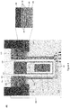
- FIG. 1 illustrates a partial cross-sectional view of an embodiment of a trench-based semiconductor device 100.
- the semiconductor device 100 includes one or more gate trenches 102 extending into a Si substrate 104.
- a single gate trench 102 is shown in Figure 1 , however the semiconductor device 100 may include a plurality of gate trenches 102 with the same or similar construction but which are out of view.
- the Si substrate 104 may comprise one or more Si epitaxial layers grown on a base Si substrate.
- a gate electrode 106 disposed in each gate trench 102 is insulated from the surrounding semiconductor material by a gate dielectric 108.
- a field electrode 110 may be disposed in each gate trench 102 below the corresponding gate electrode 106, and insulated from the surrounding semiconductor material and the gate electrode 106 by a field dielectric 112.
- the gate and field dielectrics 108, 112 may comprise the same or different materials, and may have the same or different thicknesses.
- the field electrode 110 instead may be formed in a different trench separate from the gate trench 102, or omitted altogether depending on the type of semiconductor device.
- an insulating spacer 111 such as a region of high-density plasma oxide vertically separates the gate electrode 106 from the field electrode 110, and a silicon nitride layer 113 separates the insulating spacer 111 and the field dielectric 112 from the gate dielectric 108 in a region of the gate trench 102 below the gate electrode 106.
- the trench-based semiconductor device 100 may be a power semiconductor device such as a power MOSFET (metal-oxide-semiconductor field effect transistor), an IGBT (insulated gate bipolar transistor), etc.
- the trench-based semiconductor device 100 further includes a body region 114 formed in the Si substrate 104.
- the body region 114 includes a channel region 116 which vertically extends along the sidewall 118 of the corresponding gate trench 102.
- the semiconductor device 100 also includes a source region 120 formed in the Si substrate 104 above the body region 114. Vertical current flow through the channel region 116 is controlled by applying a gate potential to the gate electrode 106.
- a drain or collector region (not shown) is formed below a drift zone 122 of the device 100.
- additional structures may be formed in the drift zone 122 and/or between the drift zone 122 and the drain/collector region.
- charge compensation structures may be formed in the drift zone 122 and/or a field stop layer may be formed between the drift zone 122 and the drain/collector region in the case of an IGBT type device.
- any type of semiconductor device with a trench gate may utilize the diffusion barrier teachings described herein.
- the trench-based semiconductor device 100 further includes a contact trench 124 which extends into the Si substrate 104.
- the contact trench 124 is separated from each adjacent gate trench 102 by a portion of the source region 120 and a portion of the body region 114.
- the contact trench 124 is filled with an electrically conductive material 126 such as doped polysilicon, metal, etc. which contacts the source region 120 at the sidewall of the contact trench 124 and a highly doped body contact region 128 at the bottom of the contact trench 124.
- the highly doped body contact region 128 at the bottom of the contact trench 124 has the same doping type as the body region 114, but at a higher concentration to provide good ohmic contact with the electrically conductive material 126 which fills the contact trench 124.
- the source region 120 and drift zone 122 are doped n-type and the body region 114, channel region 116 and highly doped body contact region 128 are doped p-type.
- the source region 120 and drift zone 122 are doped p-type and the body region 114, channel region 116 and highly doped body contact region 128 are doped n-type.
- the gate and contact trenches 102, 124 extend into the Si substrate 104 from the same front surface 130.
- a diffusion barrier structure 132 extends along the sidewall 118 and bottom of the gate trench 102, and is disposed between the channel region 116 and the neighboring highly doped body contact region 128.
- the diffusion barrier structure 132 comprises alternating layers of Si 134 and oxygen-doped Si 136.
- the alternating layers of Si 134 and oxygen-doped Si 136 form an oxygen-doped silicon region grown by epitaxy.
- the oxygen concentration for each oxygen-doped Si layer 136 is below 5e14cm-3.
- Each oxygen-doped Si layer 136 may have a thickness in the atomic range (e.g. one or several atoms thick) or in the nanometer range to ensure sufficient crystal information for growing Si on the oxygen-doped Si layers 136.
- the alternating layers of Si 134 and oxygen-doped Si 136 may be realized by epitaxially growing Si layers alternating with oxygen layers respectively adsorbed on surfaces of the Si layers, e.g., with a particular limited thickness for the oxygen-doped Si layers 136 to ensure adequate Si growth.
- Figure 1 provides an exploded view of the diffusion barrier structure 132, which may also include a Si buffer layer 138 below the alternating layers of Si 134 and oxygen-doped Si 136, and a capping layer 140 of Si epitaxially grown on the alternating layers of Si 134 and oxygen-doped Si 136.
- the Si buffer layer 138 may be relatively thin, e.g., in the range of 2-5 nm thick.
- the Si buffer layer 138 may be grown after an implant or an etch step.
- the capping layer 140 provides high carrier mobility in this region of the device 100.
- the channel region 116 is formed in the Si capping layer 140 and vertically extends along the sidewall 118 of the gate trench 102.
- the buffer layer 138 may be omitted.
- the oxygen-doped Si layers 136 of the diffusion barrier structure 132 limit the lateral out-diffusion of the source/body contact doping, thereby controlling lateral out-diffusion from each highly doped body contact region 128 in a direction towards the channel region 116.
- the oxygen-doped Si layers 136 of the diffusion barrier structure 132 may also improve carrier mobility within the vertical channel region 116 of the device 100.
- the oxygen-doped Si layers 136 of the diffusion barrier structure 132 may be formed by introducing oxygen partial monolayers to a Si lattice.
- the oxygen atoms are interstitially placed to minimize disruption to the Si lattice.
- Layers of Si atoms 134 separate adjacent oxygen partial monolayers 136.
- the alternating layers of Si 134 and oxygen-doped Si 136 may be formed by Si epitaxy with absorption of oxygen at different steps. For example, temperature and gaseous conditions can be controlled during the epitaxy process to form the partial oxygen monolayers 136.
- Oxygen may be introduced/incorporated between epitaxial layers 134 of Si, e.g. by controlling the introduction of an oxygen precursor into the epitaxy chamber.
- the resulting barrier barrier structure 132 includes monolayers 136 that comprise mainly Si but have a doped level or concentration level of oxygen alternating with standard epitaxial layers 134 of Si without oxygen.
- the diffusion barrier structure 132 also comprises a capping layer 140 of Si epitaxially grown on the alternating layers of Si 134 and oxygen-doped Si 136, or the capping layer 140 of Si may be omitted.
- the capping layer 140 of epitaxial Si is doped to form the channel region 116 of the device 100.
- the diffusion barrier structure 132 may extend over an upper side 115 of the body region 114 and be disposed between the source region 120 and the body region 114 at the upper side of the body region 114.
- the current pathway includes the source region 120, the channel region 116 and the drift zone 122. Current spreads outward from the channel region 116 as the current pathway vertically progresses into the drift zone 122, as indicated by the dashed lines in Figure 1 .
- Figures 2A through 2M illustrate respective cross-sectional views of the trench-based semiconductor device 100 shown in Figure 1 during different stages of a manufacturing process.
- Figure 2A shows the semiconductor device 100 after formation of the gate trench 102.
- the gate trench 102 may be etched into the Si substrate 104 using any common trench formation process such as applying a mask / insulating material 200 on the front main surface 130 of the Si substrate 104 and etching the gate trench 102 into the Si substrate 104 through an opening 201 in the mask 200.
- Figure 2B shows the semiconductor device 100 after the alternating layers of Si 134 and oxygen-doped Si 136 of the diffusion barrier structure 132 are epitaxially grown on the sidewall 118 and the bottom of the gate trench 102.
- the alternating layers of Si 134 and oxygen-doped Si 136 are epitaxially grown on the sidewall 118 and the bottom of the gate trench 102 after etching the gate trench 102 into the Si substrate 104 but before forming the gate electrode 106 and the gate dielectric 108 in the gate trench 102.
- Figure 2C shows the semiconductor device 100 after a capping layer 140 of Si is epitaxially grown on the alternating layers of Si 134 and oxygen-doped Si 136 to form the diffusion barrier structure 132.
- the capping layer 140 of epitaxial Si has the same standard in situ doping concentration as the alternating layers of Si 134 and oxygen-doped Si 136 and may be doped later with a different dopant species and concentration to form the channel region 116 of the semiconductor device 100.
- the capping layer 140 may have a different in situ doping concentration compared to the alternating layers of Si 134 and oxygen-doped Si 136. In either case, the capping layer 140 may be used to implement the channel region 116 of the semiconductor device 100.
- Figure 2D shows the semiconductor device 100 after the gate dielectric 108 is formed along the diffusion barrier structure 132.
- Any common semiconductor manufacturing process for forming a gate dielectric may be used, e.g., such as a deposition process, a thermal oxidation process, or both a deposition process and a thermal oxidation process.
- Figure 2E shows the semiconductor device 100 after a silicon nitride layer 113 is formed on the gate dielectric 108.
- Any common semiconductor manufacturing process for forming a silicon nitride layer may be used, e.g., such as low pressure chemical vapor deposition (LPCVD), plasma-enhanced chemical vapor deposition (PECVD), etc.
- LPCVD low pressure chemical vapor deposition
- PECVD plasma-enhanced chemical vapor deposition
- Figure 2F shows the semiconductor device 100 after a field dielectric 112 such as a field oxide is formed on the silicon nitride layer 113, and after forming the field dielectric 1121, the gate trench 102 is filled with a first electrically conductive material 202 such as doped polysilicon, metal, etc.
- a field dielectric 112 such as a field oxide
- the gate trench 102 is filled with a first electrically conductive material 202 such as doped polysilicon, metal, etc.
- Figure 2G shows the semiconductor device 100 after the first electrically conductive material 202 is recessed to a first depth D1 in the gate trench 102 to form the field electrode 110.
- Any common semiconductor manufacturing process for recessing an electrode material in a trench may be used, e.g., such as plasma etching, etc.
- Figure 2H shows the semiconductor device 100 after the field dielectric 112 is removed from the gate trench 102 above the field electrode 110 to expose the silicon nitride layer 113 in a region of the gate trench 102 above the field electrode 110.
- Any common semiconductor manufacturing process for removing a field dielectric from a trench may be used, e.g., such as HF etching, etc.
- Figure 2I shows the semiconductor device 100 after the gate trench 102 is filled with a dielectric material 204.
- the gate trench 102 is filled with a silicon-based dielectric such as silicon oxide using a high-density plasma chemical vapor deposition (HDP CVD) process.
- HDP CVD high-density plasma chemical vapor deposition
- Other processes may be used to produce a void-free gate trench 102, such as a multistep deposition/etch process, a spin-on dielectric process, etc.
- Figure 2J shows the semiconductor device 100 after the dielectric material 204 is recessed to a second depth D2 in the gate trench 102 above the field electrode 110, wherein D2 ⁇ D1.
- Any common semiconductor manufacturing process for recessing dielectric material in a trench may be used, e.g., such as HF etching in the case of oxide, etc.
- the part of the dielectric material 204 that remains in the gate trench 102 forms an insulating spacer 111 which covers the field electrode 110.
- the insulating spacer 111 instead may be a thermal oxide.
- the oxygen-doped Si layers 136 of the diffusion barrier structure 132 can be protected during the thermal oxidation process by using a lower thermal oxidation temperature than what is commonly used to form a thermal oxide.
- Figure 2K shows the semiconductor device 100 after the silicon nitride layer 113 is removed from the gate trench 102 above the insulating spacer 111.
- Any common semiconductor manufacturing process for removing silicon nitride from a trench may be used, e.g., such as wet etching, plasma etching, etc.
- the gate trench 102 is filled with a second electrically conductive material 206 such as doped polysilicon, a metal, etc.
- Figure 2L shows the semiconductor device 100 after the second electrically conductive material 206 is recessed to a third depth D3 in the gate trench 102 to form the gate electrode 106, wherein D3 ⁇ D2.
- Any common semiconductor manufacturing process for recessing a gate electrode material in a trench may be used, e.g., such as plasma etching, wet etching, etc.
- Figure 2M shows the semiconductor device 100 after dopant species of the opposite conductivity type are implanted into the Si substrate 104 and activated by annealing to form the body and the source regions 114, 120 of the device 100.
- the source dopants may be phosphorus, arsenic, etc. and the body dopants may be boron, gallium, etc.
- the source dopants may be boron, gallium, etc. and the body dopants may be phosphorus, arsenic, etc.
- the contact trenches 124 may be formed after implanting the dopant species of the opposite conductivity type into the Si substrate 104 to form the body and the source regions 114, 120 of the device 100.
- the contact trenches 124 may be etched into the front main surface 130 of the Si substrate 104, implanted through the trench bottom to form a highly doped body contact region 128 at the bottom of the contact trench 124, and then filled with an electrically conductive material 126 which contacts the source region 120 at the sidewall of the contact trench 124 and the highly doped body contact region 128 at the bottom of the contact trench 124, e.g., as shown in Figure 1 .
- Figure 3 illustrates a partial cross-sectional view of another embodiment of a trench-based semiconductor device 300 having a diffusion barrier structure 132 that comprises alternating layers of Si 134 and oxygen-doped Si 136 and a capping layer 140 of Si epitaxially grown on the alternating layers of Si 134 and oxygen-doped Si 136, wherein the channel region 116 of the device 300 is formed in the Si capping layer 140 and vertically extends along the sidewall 118 of the gate trench 102.
- the embodiment shown in Figure 3 is similar to the embodiment shown in Figure 1 .
- the diffusion barrier structure 132 of the device 300 shown in Figure 3 also extends onto the front main surface 130 of the Si substrate 104 into which the gate trench 102 and the contact trench 126 are formed.
- the diffusion barrier structure 132 extends along the front main surface 130 of the Si substrate 104 to the electrically conductive material 126 which fills the contact trench 126.
- the diffusion barrier structure 132 may be formed in this way by removing the mask / insulating material 200 shown in Figure 2A after etching the gate trench 102 into the Si substrate 104 and before forming the alternating layers of Si 134 and oxygen-doped Si 136. This way, the diffusion barrier structure 132 will also epitaxially grow on the front main surface 130 of the Si substrate 104.
- Figure 4 illustrates a partial cross-sectional view of another embodiment of a trench-based semiconductor device 400 having a diffusion barrier structure 132 that comprises alternating layers of Si 134 and oxygen-doped Si 136 and a capping layer 140 of Si epitaxially grown on the alternating layers of Si 134 and oxygen-doped Si 136, wherein the channel region 116 of the device 400 is formed in the Si capping layer 140 and vertically extends along the sidewall of the gate trench 102.
- the embodiment shown in Figure 4 is similar to the embodiment shown in Figure 3 . Different, however, the Si capping layer 140 of the diffusion barrier structure 132 is present along the bottom of the gate trench 102 but not the alternating layers of Si 134 and oxygen-doped Si 136. Omitting the alternating layers of Si 134 and oxygen-doped Si 136 from the bottom of the gate trench 102 allows current spreading near the bottom of the gate trench 102, as indicated by the dashed arrows in Figure 4 .
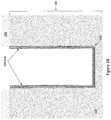
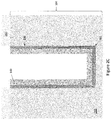
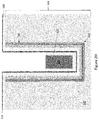
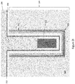
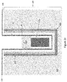
- Figures 5A through 5F illustrate an embodiment of a method of omitting the alternating layers of Si 134 and oxygen-doped Si 136 of the diffusion barrier structure 132 from the bottom of the gate trench 102.
- Figure 5A shows the semiconductor device 400 after formation of the gate trench 102.
- the gate trench 102 may be etched into the Si substrate 104 using any common trench formation process such as applying a mask / insulating material 200 on the front main surface 130 of the Si substrate 104 and etching the gate trench 102 into the Si substrate 104 through an opening 201 in the mask 200.
- Figure 5B shows the semiconductor device 400 after an insulating material 500 such as an HDP oxide is formed on the sidewall 118 and bottom of the gate trench 102.
- an insulating material 500 such as an HDP oxide
- the HDP oxide may be thinner (T1) along the sidewall 118 and thicker (T2) on the bottom of the gate trench 102.
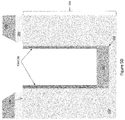
- Figure 5C shows the semiconductor device 400 after the insulating material 500 is removed from the sidewall 118 of the gate trench 102.
- the HDP oxide will be removed from the sidewall 118 of the gate trench 102 before being completely removed from the trench bottom.
- the part of the HDP oxide that remains in the bottom of the gate trench 102 forms an insulating spacer 502 in the lower part of the gate trench 102.
- the insulating spacer 502 covers the bottom and a lower part of the sidewall 118 of the gate trench 102 to prevent formation of the alternating layers of Si 134 and oxygen-doped Si 136 of the diffusion barrier structure 132 on the bottom and the lower part of the sidewall 118 of the gate trench 102.
- Figure 5D shows the semiconductor device 400 after epitaxially growing the alternating layers of Si 134 and oxygen-doped Si 136 on the exposed sidewall 118 of the gate trench 102.
- Figure 5E shows the semiconductor device 400 after the insulating spacer 502 is removed from the bottom of the gate trench 102, and after removal of any remnants of the insulating material 500 and of the mask / insulating material 200 from the front main surface 130 of the Si substrate 104.
- the lower part 504 of the sidewall 118 of the gate trench 102 and the bottom 506 of the gate trench 102 are exposed by removing the insulating spacer 502.
- Figure 5F shows the semiconductor device 400 after the Si capping layer 140 of the diffusion structure 132 is epitaxially grown on the front main surface 130 of the Si substrate 104, on the alternating layers of Si 134 and oxygen-doped Si 136, on the exposed lower part 504 of the sidewall 118 of the gate trench 102, and on the exposed bottom 506 of the gate trench 102.
- Device processing continues, e.g., as shown in Figures 2D through 2M and as previously described herein, to complete the device 400 shown in Figure 4 .
- Figures 6A through 6H illustrate another embodiment of a method of omitting the alternating layers of Si 134 and oxygen-doped Si 136 of the diffusion barrier structure 132 from the bottom of the gate trench 102.
- Figure 6A shows the semiconductor device 400 after formation of the gate trench 102.
- the gate trench 102 may be etched into the Si substrate 104 using any common trench formation process such as applying a mask / insulating material 200 on the front main surface 130 of the Si substrate 104 and etching the gate trench 102 into the Si substrate 104 through an opening 201 in the mask 200.
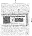
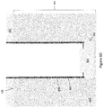
- Figure 6B shows the semiconductor device 400 after an oxide layer 600 is formed on the sidewall 118 and bottom of the gate trench 102, e.g., by deposition, thermal oxidation, or a combination of both, and after a silicon nitride layer 602 is formed on the oxide layer 600 over the sidewall 118 and bottom of the gate trench 102.
- Figure 6C shows the semiconductor device 400 after an opening 604 is formed in the silicon nitride layer 602 at the bottom of the gate trench 102, e.g., by anisotropic plasma etching, to expose the silicon oxide layer 600 at the trench bottom.
- Figure 6D shows the semiconductor device 400 after thermally oxidizing a region of the Si substrate 104 below the exposed silicon oxide layer 600 at the bottom of the gate trench 102.
- the thermal oxidation process yields an insulating spacer 606 in the lower part of the gate trench 102.
- the insulating spacer 606 covers the bottom and a lower part of the sidewall 118 of the gate trench 102 to prevent formation of the alternating layers of Si 134 and oxygen-doped Si 136 of the diffusion barrier structure 132 on the bottom and the lower part of the sidewall 118 of the gate trench 102.
- Figure 6E shows the semiconductor device 400 after the silicon nitride layer 602 and the silicon oxide layer 600 are removed from the sidewall 118 of the gate trench 102.
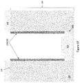
- Figure 6F shows the semiconductor device 400 after epitaxially growing the alternating layers of Si and oxygen-doped Si on the exposed sidewall 118 of the gate trench 102.
- Figure 6G shows the semiconductor device 400 after the insulating spacer 606 is removed from the bottom of the gate trench 102, and after removal of any remnants of the mask / insulating material 200 from the front main surface 130 of the Si substrate 104.
- the lower part 608 of the sidewall 118 of the gate trench 102 and the bottom 610 of the gate trench 102 are exposed by removing the insulating spacer 606.
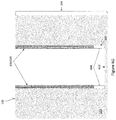
- Figure 6H shows the semiconductor device 400 after the Si capping layer 140 of the diffusion structure 132 is epitaxially grown on the front main surface 130 of the Si substrate 104, on the alternating layers of Si 134 and oxygen-doped Si 136, on the exposed lower part 608 of the sidewall 118 of the gate trench 102, and on the exposed bottom 610 of the gate trench 102.
- Device processing continues, e.g., as shown in Figures 2D through 2M and as previously described herein, to complete the device 400 shown in Figure 4 .
Landscapes
- Electrodes Of Semiconductors (AREA)
- Chemical & Material Sciences (AREA)
- Chemical Kinetics & Catalysis (AREA)
- Crystallography & Structural Chemistry (AREA)
- General Chemical & Material Sciences (AREA)
Abstract
Description
- As the dimensions of trench-based transistors shrink, the influence of the highly-doped source/body contact on the net body doping near the channel region becomes more important. For wider lateral distribution of the source/body contact diffusion with 2-3 orders of magnitude higher doping levels compared to the body doping, Vth (threshold voltage) and RonA (on-state resistance) of the device increases. Increasing the distance between the source/body contact and the channel region causes depletion of the body at high drain voltages which can lead to high DIBL (drain-induced barrier lowering). Furthermore, the process window variation for both trench width and contact width as well as contact misalignment must become smaller to avoid these adverse effects (higher Vth, higher RonA and higher DIBL).
- Hence, better control of the lateral out-diffusion of the source/body contact doping is desirable.
- According to an embodiment of a semiconductor device, the semiconductor device comprises: a gate trench extending into a Si substrate; a body region in the Si substrate adjacent the gate trench; a source region in the Si substrate above the body region; a contact trench extending into the Si substrate and filled with an electrically conductive material which contacts the source region at a sidewall of the contact trench and a highly doped body contact region at a bottom of the contact trench; a diffusion barrier structure formed along the sidewall of the gate trench, the diffusion barrier structure comprising alternating layers of Si and oxygen-doped Si and a Si capping layer on the alternating layers of Si and oxygen-doped Si; and a channel region formed in the Si capping layer and which vertically extends along the sidewall of the gate trench.
- In an embodiment, the diffusion barrier structure may extend onto a front main surface of the Si substrate into which the gate trench and the contact trench are formed.
- Separately or in combination, the diffusion barrier structure may extend along the front main surface of the Si substrate to the electrically conductive material which fills the contact trench.
- Separately or in combination, the Si capping layer of the diffusion barrier structure may be present along the bottom of the gate trench but not the alternating layers of Si and oxygen-doped Si.
- Separately or in combination, the gate trench may comprise a gate dielectric lining the sidewall and a bottom of the gate trench, a gate electrode disposed in an upper part of the gate trench, a field electrode embedded in a field dielectric in a lower part of the gate trench below the gate electrode, an insulating spacer vertically separating the gate electrode from the field electrode, and a silicon nitride layer separating the insulating spacer and the field dielectric from the gate dielectric.
- According to an embodiment of a method of manufacturing a semiconductor device, the method comprises: forming a gate trench which extends into a Si substrate; forming a body region in the Si substrate adjacent the gate trench; forming a source region in the Si substrate above the body region; forming a contact trench which extends into the Si substrate and is filled with an electrically conductive material which contacts the source region at a sidewall of the contact trench and a highly doped body contact region at a bottom of the contact trench; forming a diffusion barrier structure along the sidewall of the gate trench, the diffusion barrier structure comprising alternating layers of Si and oxygen-doped Si and a Si capping layer on the alternating layers of Si and oxygen-doped Si; and forming a channel region in the Si capping layer and which vertically extends along the sidewall of the gate trench.
- In an embodiment, forming the diffusion barrier structure may comprise: epitaxially growing the alternating layers of Si and oxygen-doped Si on the sidewall and a bottom of the gate trench; and epitaxially growing the Si capping layer on the alternating layers of Si and oxygen-doped Si.
- Separately or in combination, the method may further comprises epitaxially growing the alternating layers of Si and oxygen-doped Si and the Si capping layer on a front main surface of the Si substrate into which the gate trench is formed.
- Separately or in combination, the method may further comprise, after forming the diffusion barrier structure, implanting dopant species of the opposite conductivity type into the Si substrate to form the body and the source regions.
- Separately or in combination, the method may further comprises forming a gate dielectric on the Si capping layer.
- Separately or in combination, the gate dielectric may be formed by a deposition process, a thermal oxidation process, or both the deposition process and the thermal oxidation process.
- Separately or in combination, the method may further comprise: forming a silicon nitride layer on the gate dielectric; forming a field dielectric on the silicon nitride layer; after forming the field dielectric, filling the gate trench with a first electrically conductive material; and recessing the first electrically conductive material to a first depth in the gate trench to form a field electrode.
- Separately or in combination, the method may further comprise: removing the field dielectric above the field electrode to expose the silicon nitride layer in a region of the gate trench above the field electrode; and after removing the field dielectric above the field electrode, covering the field electrode with an insulating spacer.
- Separately or in combination, covering the field electrode with the insulating spacer may comprise: after removing the field oxide above the field electrode, filling the gate trench with a dielectric material; and recessing the dielectric material to a second depth in the gate trench above the field electrode.
- Separately or in combination, filling the gate trench with the dielectric material may comprise depositing a high-density-plasma oxide in the gate trench by chemical vapor deposition.
- Separately or in combination, covering the field electrode with the insulating spacer may comprise forming a thermal oxide on the field electrode by a thermal oxidation process.
- Separately or in combination, the method may further comprise: removing the silicon nitride layer above the insulating spacer; after removing the silicon nitride layer above the insulating spacer, filling the gate trench with a second electrically conductive material; and recessing the second electrically conductive material to a third depth in the gate trench to form a gate electrode.
- Separately or in combination, the method may further comprise, after forming the gate electrode, implanting dopant species of the opposite conductivity type into the Si substrate to form the body and the source regions.
- Separately or in combination, the contact trench may be formed after implanting the dopant species of the opposite conductivity type into the Si substrate.
- Separately or in combination, the method may further comprise: removing the silicon nitride layer above the insulating spacer; after removing the silicon nitride layer above the insulating spacer, filling the gate trench with a second electrically conductive material; and recessing the second electrically conductive material to a third depth in the gate trench to form a gate electrode.
- Separately or in combination, the method may further comprise: before forming the alternating layers of Si and oxygen-doped Si of the diffusion barrier structure, forming an insulating spacer in a lower part of the gate trench, the insulating spacer covering a bottom and a lower part of the sidewall of the gate trench to prevent formation of the alternating layers of Si and oxygen-doped Si of the diffusion barrier structure on the bottom and the lower part of the sidewall of the gate trench; and after forming the alternating layers of Si and oxygen-doped Si of the diffusion barrier structure, removing the insulating spacer from the lower part of the gate trench.
- Separately or in combination, the method may further comprise after removing the insulating spacer from the lower part of the gate trench, epitaxially growing the Si capping layer of the diffusion barrier structure on the alternating layers of Si and oxygen-doped Si and on the bottom and the lower part of the sidewall of the gate trench.
- Separately or in combination, forming the insulating spacer in the lower part of the gate trench may comprise: forming a high-density plasma oxide on the sidewall and the bottom of the gate trench, the high-density plasma oxide being thinner along the sidewall and thicker on the bottom of the gate trench; and removing the high-density plasma oxide from the sidewall of the gate trench.
- Separately or in combination, forming the insulating spacer in the lower part of the gate trench may comprise: forming a silicon oxide layer on the sidewall and the bottom of the gate trench; forming a silicon nitride layer on the silicon oxide layer over the sidewall and the bottom of the gate trench; forming an opening in the silicon nitride layer at the bottom of the gate trench to expose the silicon oxide layer at the bottom of the gate trench; thermally oxidizing a region of the Si substrate below the exposed silicon oxide layer at the bottom of the gate trench; and removing the silicon nitride layer and the silicon oxide layer from the sidewall of the gate trench.
- Those skilled in the art will recognize additional features and advantages upon reading the following detailed description, and upon viewing the accompanying drawings.
- The elements of the drawings are not necessarily to scale relative to each other. Like reference numerals designate corresponding similar parts. The features of the various illustrated embodiments may be combined unless they exclude each other. Embodiments are depicted in the drawings and are detailed in the description which follows.
-
Figure 1 illustrates a partial cross-sectional view of an embodiment of a trench-based semiconductor device having a diffusion barrier structure. -
Figure 2A through 2M illustrate respective cross-sectional views of the trench-based semiconductor device shown inFigure 1 during different stages of a manufacturing process. -
Figure 3 illustrates a partial cross-sectional view of another embodiment of a trench-based semiconductor device having a diffusion barrier structure. -
Figure 4 illustrates a partial cross-sectional view of another embodiment of a trench-based semiconductor device having a diffusion barrier structure. -
Figure 5A through 5F illustrate respective cross-sectional views of the trench-based semiconductor device shown inFigure 4 during different stages of a manufacturing process for forming the diffusion barrier structure. -
Figure 6A through 6H illustrate respective cross-sectional views of the trench-based semiconductor device shown inFigure 4 during different stages of another manufacturing process for forming the diffusion barrier structure. - Embodiments described herein control lateral out-diffusion of the source/body contact doping for trench-based transistors, allowing for narrower Vth, RonA and DIBL distributions for a given geometry variation for the highly-doped source/body contact and gate trench, and/or allowing for a lateral spacing reduction between the source/body contact and channel region of the device for given Vth, RonA and DIBL windows. The lateral out-diffusion of the source/body contact doping is better controlled by inserting a diffusion barrier structure which extends along at least part of the channel region of the device. The diffusion barrier structure comprises alternating layers of Si and oxygen-doped Si disposed between the highly doped source/body contact and the channel region of the device. The oxygen-doped Si layers of the diffusion barrier structure limit the lateral out-diffusion of the source/body contact doping, thereby controlling the lateral out-diffusion of the source/body contact doping in a direction towards the channel region. The diffusion barrier structure enables, for example, narrower Vth distribution for a narrow-trench MOSFET, or for a predetermined Vth distribution width, a smaller distance between the contact trench and the gate trench. Charge carrier mobility in the channel region may be increased, e.g., by up to 80% by incorporating the diffusion barrier structure. Gate leakage may also be reduced by incorporating the diffusion barrier structure, e.g., by up to 50%, and gate reliability improved compared to gate oxides grown on conventional silicon epitaxial layers. Described next in more detail are embodiments of semiconductor devices with such a diffusion barrier structure, and corresponding methods of manufacture.
-
Figure 1 illustrates a partial cross-sectional view of an embodiment of a trench-basedsemiconductor device 100. Thesemiconductor device 100 includes one ormore gate trenches 102 extending into aSi substrate 104. Asingle gate trench 102 is shown inFigure 1 , however thesemiconductor device 100 may include a plurality ofgate trenches 102 with the same or similar construction but which are out of view. TheSi substrate 104 may comprise one or more Si epitaxial layers grown on a base Si substrate. Agate electrode 106 disposed in eachgate trench 102 is insulated from the surrounding semiconductor material by a gate dielectric 108. Afield electrode 110 may be disposed in eachgate trench 102 below thecorresponding gate electrode 106, and insulated from the surrounding semiconductor material and thegate electrode 106 by a field dielectric 112. The gate andfield dielectrics field electrode 110 instead may be formed in a different trench separate from thegate trench 102, or omitted altogether depending on the type of semiconductor device. In one embodiment, aninsulating spacer 111 such as a region of high-density plasma oxide vertically separates thegate electrode 106 from thefield electrode 110, and asilicon nitride layer 113 separates theinsulating spacer 111 and the field dielectric 112 from the gate dielectric 108 in a region of thegate trench 102 below thegate electrode 106. - The trench-based
semiconductor device 100 may be a power semiconductor device such as a power MOSFET (metal-oxide-semiconductor field effect transistor), an IGBT (insulated gate bipolar transistor), etc. The trench-basedsemiconductor device 100 further includes abody region 114 formed in theSi substrate 104. Thebody region 114 includes achannel region 116 which vertically extends along thesidewall 118 of thecorresponding gate trench 102. Thesemiconductor device 100 also includes asource region 120 formed in theSi substrate 104 above thebody region 114. Vertical current flow through thechannel region 116 is controlled by applying a gate potential to thegate electrode 106. A drain or collector region (not shown) is formed below adrift zone 122 of thedevice 100. Depending on the type of device, additional structures may be formed in thedrift zone 122 and/or between thedrift zone 122 and the drain/collector region. For example, charge compensation structures may be formed in thedrift zone 122 and/or a field stop layer may be formed between thedrift zone 122 and the drain/collector region in the case of an IGBT type device. Again, any type of semiconductor device with a trench gate may utilize the diffusion barrier teachings described herein. - The trench-based
semiconductor device 100 further includes acontact trench 124 which extends into theSi substrate 104. Thecontact trench 124 is separated from eachadjacent gate trench 102 by a portion of thesource region 120 and a portion of thebody region 114. Thecontact trench 124 is filled with an electricallyconductive material 126 such as doped polysilicon, metal, etc. which contacts thesource region 120 at the sidewall of thecontact trench 124 and a highly dopedbody contact region 128 at the bottom of thecontact trench 124. - The highly doped
body contact region 128 at the bottom of thecontact trench 124 has the same doping type as thebody region 114, but at a higher concentration to provide good ohmic contact with the electricallyconductive material 126 which fills thecontact trench 124. For example, in the case of an n-channel device, thesource region 120 and driftzone 122 are doped n-type and thebody region 114,channel region 116 and highly dopedbody contact region 128 are doped p-type. Conversely, in the case of an p-channel device, thesource region 120 and driftzone 122 are doped p-type and thebody region 114,channel region 116 and highly dopedbody contact region 128 are doped n-type. In either case, the gate andcontact trenches Si substrate 104 from the samefront surface 130. - A
diffusion barrier structure 132 extends along thesidewall 118 and bottom of thegate trench 102, and is disposed between thechannel region 116 and the neighboring highly dopedbody contact region 128. Thediffusion barrier structure 132 comprises alternating layers ofSi 134 and oxygen-dopedSi 136. The alternating layers ofSi 134 and oxygen-dopedSi 136 form an oxygen-doped silicon region grown by epitaxy. In an embodiment, the oxygen concentration for each oxygen-dopedSi layer 136 is below 5e14cm-3. Each oxygen-dopedSi layer 136 may have a thickness in the atomic range (e.g. one or several atoms thick) or in the nanometer range to ensure sufficient crystal information for growing Si on the oxygen-doped Si layers 136. The alternating layers ofSi 134 and oxygen-dopedSi 136 may be realized by epitaxially growing Si layers alternating with oxygen layers respectively adsorbed on surfaces of the Si layers, e.g., with a particular limited thickness for the oxygen-doped Si layers 136 to ensure adequate Si growth. -
Figure 1 provides an exploded view of thediffusion barrier structure 132, which may also include aSi buffer layer 138 below the alternating layers ofSi 134 and oxygen-dopedSi 136, and acapping layer 140 of Si epitaxially grown on the alternating layers ofSi 134 and oxygen-dopedSi 136. TheSi buffer layer 138 may be relatively thin, e.g., in the range of 2-5 nm thick. TheSi buffer layer 138 may be grown after an implant or an etch step. Thecapping layer 140 provides high carrier mobility in this region of thedevice 100. Thechannel region 116 is formed in theSi capping layer 140 and vertically extends along thesidewall 118 of thegate trench 102. Thebuffer layer 138 may be omitted. The oxygen-doped Si layers 136 of thediffusion barrier structure 132 limit the lateral out-diffusion of the source/body contact doping, thereby controlling lateral out-diffusion from each highly dopedbody contact region 128 in a direction towards thechannel region 116. The oxygen-doped Si layers 136 of thediffusion barrier structure 132 may also improve carrier mobility within thevertical channel region 116 of thedevice 100. - The oxygen-doped Si layers 136 of the
diffusion barrier structure 132 may be formed by introducing oxygen partial monolayers to a Si lattice. The oxygen atoms are interstitially placed to minimize disruption to the Si lattice. Layers ofSi atoms 134 separate adjacent oxygenpartial monolayers 136. The alternating layers ofSi 134 and oxygen-dopedSi 136 may be formed by Si epitaxy with absorption of oxygen at different steps. For example, temperature and gaseous conditions can be controlled during the epitaxy process to form thepartial oxygen monolayers 136. Oxygen may be introduced/incorporated betweenepitaxial layers 134 of Si, e.g. by controlling the introduction of an oxygen precursor into the epitaxy chamber. The resultingbarrier barrier structure 132 includesmonolayers 136 that comprise mainly Si but have a doped level or concentration level of oxygen alternating with standard epitaxial layers 134 of Si without oxygen. Thediffusion barrier structure 132 also comprises acapping layer 140 of Si epitaxially grown on the alternating layers ofSi 134 and oxygen-dopedSi 136, or thecapping layer 140 of Si may be omitted. Thecapping layer 140 of epitaxial Si is doped to form thechannel region 116 of thedevice 100. In addition or alternatively, thediffusion barrier structure 132 may extend over anupper side 115 of thebody region 114 and be disposed between thesource region 120 and thebody region 114 at the upper side of thebody region 114. - Current flows through the high
mobility channel region 116 of thesemiconductor device 100 by applying a gate potential (represented by '-ve bias' inFigure 2 ) to thegate electrode 106. The current pathway includes thesource region 120, thechannel region 116 and thedrift zone 122. Current spreads outward from thechannel region 116 as the current pathway vertically progresses into thedrift zone 122, as indicated by the dashed lines inFigure 1 . -
Figures 2A through 2M illustrate respective cross-sectional views of the trench-basedsemiconductor device 100 shown inFigure 1 during different stages of a manufacturing process. -
Figure 2A shows thesemiconductor device 100 after formation of thegate trench 102. Thegate trench 102 may be etched into theSi substrate 104 using any common trench formation process such as applying a mask / insulatingmaterial 200 on the frontmain surface 130 of theSi substrate 104 and etching thegate trench 102 into theSi substrate 104 through anopening 201 in themask 200. -
Figure 2B shows thesemiconductor device 100 after the alternating layers ofSi 134 and oxygen-dopedSi 136 of thediffusion barrier structure 132 are epitaxially grown on thesidewall 118 and the bottom of thegate trench 102. According to this embodiment, the alternating layers ofSi 134 and oxygen-dopedSi 136 are epitaxially grown on thesidewall 118 and the bottom of thegate trench 102 after etching thegate trench 102 into theSi substrate 104 but before forming thegate electrode 106 and thegate dielectric 108 in thegate trench 102. -
Figure 2C shows thesemiconductor device 100 after acapping layer 140 of Si is epitaxially grown on the alternating layers ofSi 134 and oxygen-dopedSi 136 to form thediffusion barrier structure 132. In one embodiment, thecapping layer 140 of epitaxial Si has the same standard in situ doping concentration as the alternating layers ofSi 134 and oxygen-dopedSi 136 and may be doped later with a different dopant species and concentration to form thechannel region 116 of thesemiconductor device 100. Alternatively, thecapping layer 140 may have a different in situ doping concentration compared to the alternating layers ofSi 134 and oxygen-dopedSi 136. In either case, thecapping layer 140 may be used to implement thechannel region 116 of thesemiconductor device 100. -
Figure 2D shows thesemiconductor device 100 after thegate dielectric 108 is formed along thediffusion barrier structure 132. Any common semiconductor manufacturing process for forming a gate dielectric may be used, e.g., such as a deposition process, a thermal oxidation process, or both a deposition process and a thermal oxidation process. -
Figure 2E shows thesemiconductor device 100 after asilicon nitride layer 113 is formed on thegate dielectric 108. Any common semiconductor manufacturing process for forming a silicon nitride layer may be used, e.g., such as low pressure chemical vapor deposition (LPCVD), plasma-enhanced chemical vapor deposition (PECVD), etc. -
Figure 2F shows thesemiconductor device 100 after afield dielectric 112 such as a field oxide is formed on thesilicon nitride layer 113, and after forming the field dielectric 1121, thegate trench 102 is filled with a first electricallyconductive material 202 such as doped polysilicon, metal, etc. -
Figure 2G shows thesemiconductor device 100 after the first electricallyconductive material 202 is recessed to a first depth D1 in thegate trench 102 to form thefield electrode 110. Any common semiconductor manufacturing process for recessing an electrode material in a trench may be used, e.g., such as plasma etching, etc. -
Figure 2H shows thesemiconductor device 100 after thefield dielectric 112 is removed from thegate trench 102 above thefield electrode 110 to expose thesilicon nitride layer 113 in a region of thegate trench 102 above thefield electrode 110. Any common semiconductor manufacturing process for removing a field dielectric from a trench may be used, e.g., such as HF etching, etc. -
Figure 2I shows thesemiconductor device 100 after thegate trench 102 is filled with adielectric material 204. In one embodiment, thegate trench 102 is filled with a silicon-based dielectric such as silicon oxide using a high-density plasma chemical vapor deposition (HDP CVD) process. Other processes may be used to produce a void-free gate trench 102, such as a multistep deposition/etch process, a spin-on dielectric process, etc. -
Figure 2J shows thesemiconductor device 100 after thedielectric material 204 is recessed to a second depth D2 in thegate trench 102 above thefield electrode 110, wherein D2 < D1. Any common semiconductor manufacturing process for recessing dielectric material in a trench may be used, e.g., such as HF etching in the case of oxide, etc. The part of thedielectric material 204 that remains in thegate trench 102 forms an insulatingspacer 111 which covers thefield electrode 110. Instead, of forming the insulatingspacer 111 from HDP oxide, the insulatingspacer 111 instead may be a thermal oxide. In this case, the oxygen-doped Si layers 136 of thediffusion barrier structure 132 can be protected during the thermal oxidation process by using a lower thermal oxidation temperature than what is commonly used to form a thermal oxide. -
Figure 2K shows thesemiconductor device 100 after thesilicon nitride layer 113 is removed from thegate trench 102 above the insulatingspacer 111. Any common semiconductor manufacturing process for removing silicon nitride from a trench may be used, e.g., such as wet etching, plasma etching, etc. After removing thesilicon nitride layer 113 above the insulatingspacer 111, thegate trench 102 is filled with a second electricallyconductive material 206 such as doped polysilicon, a metal, etc. -
Figure 2L shows thesemiconductor device 100 after the second electricallyconductive material 206 is recessed to a third depth D3 in thegate trench 102 to form thegate electrode 106, wherein D3 < D2. Any common semiconductor manufacturing process for recessing a gate electrode material in a trench may be used, e.g., such as plasma etching, wet etching, etc. -
Figure 2M shows thesemiconductor device 100 after dopant species of the opposite conductivity type are implanted into theSi substrate 104 and activated by annealing to form the body and thesource regions device 100. In the case of an n-channel device, the source dopants may be phosphorus, arsenic, etc. and the body dopants may be boron, gallium, etc. In the case of a p-channel device, the source dopants may be boron, gallium, etc. and the body dopants may be phosphorus, arsenic, etc. - The
contact trenches 124 may be formed after implanting the dopant species of the opposite conductivity type into theSi substrate 104 to form the body and thesource regions device 100. For example, thecontact trenches 124 may be etched into the frontmain surface 130 of theSi substrate 104, implanted through the trench bottom to form a highly dopedbody contact region 128 at the bottom of thecontact trench 124, and then filled with an electricallyconductive material 126 which contacts thesource region 120 at the sidewall of thecontact trench 124 and the highly dopedbody contact region 128 at the bottom of thecontact trench 124, e.g., as shown inFigure 1 . -
Figure 3 illustrates a partial cross-sectional view of another embodiment of a trench-basedsemiconductor device 300 having adiffusion barrier structure 132 that comprises alternating layers ofSi 134 and oxygen-dopedSi 136 and acapping layer 140 of Si epitaxially grown on the alternating layers ofSi 134 and oxygen-dopedSi 136, wherein thechannel region 116 of thedevice 300 is formed in theSi capping layer 140 and vertically extends along thesidewall 118 of thegate trench 102. The embodiment shown inFigure 3 is similar to the embodiment shown inFigure 1 . Different, however, thediffusion barrier structure 132 of thedevice 300 shown inFigure 3 also extends onto the frontmain surface 130 of theSi substrate 104 into which thegate trench 102 and thecontact trench 126 are formed. In one embodiment, thediffusion barrier structure 132 extends along the frontmain surface 130 of theSi substrate 104 to the electricallyconductive material 126 which fills thecontact trench 126. Thediffusion barrier structure 132 may be formed in this way by removing the mask / insulatingmaterial 200 shown inFigure 2A after etching thegate trench 102 into theSi substrate 104 and before forming the alternating layers ofSi 134 and oxygen-dopedSi 136. This way, thediffusion barrier structure 132 will also epitaxially grow on the frontmain surface 130 of theSi substrate 104. -
Figure 4 illustrates a partial cross-sectional view of another embodiment of a trench-basedsemiconductor device 400 having adiffusion barrier structure 132 that comprises alternating layers ofSi 134 and oxygen-dopedSi 136 and acapping layer 140 of Si epitaxially grown on the alternating layers ofSi 134 and oxygen-dopedSi 136, wherein thechannel region 116 of thedevice 400 is formed in theSi capping layer 140 and vertically extends along the sidewall of thegate trench 102. The embodiment shown inFigure 4 is similar to the embodiment shown inFigure 3 . Different, however, theSi capping layer 140 of thediffusion barrier structure 132 is present along the bottom of thegate trench 102 but not the alternating layers ofSi 134 and oxygen-dopedSi 136. Omitting the alternating layers ofSi 134 and oxygen-dopedSi 136 from the bottom of thegate trench 102 allows current spreading near the bottom of thegate trench 102, as indicated by the dashed arrows inFigure 4 . -
Figures 5A through 5F illustrate an embodiment of a method of omitting the alternating layers ofSi 134 and oxygen-dopedSi 136 of thediffusion barrier structure 132 from the bottom of thegate trench 102. -
Figure 5A shows thesemiconductor device 400 after formation of thegate trench 102. Thegate trench 102 may be etched into theSi substrate 104 using any common trench formation process such as applying a mask / insulatingmaterial 200 on the frontmain surface 130 of theSi substrate 104 and etching thegate trench 102 into theSi substrate 104 through anopening 201 in themask 200. -
Figure 5B shows thesemiconductor device 400 after an insulatingmaterial 500 such as an HDP oxide is formed on thesidewall 118 and bottom of thegate trench 102. In the case of an HDP oxide as the insulatingmaterial 500, the HDP oxide may be thinner (T1) along thesidewall 118 and thicker (T2) on the bottom of thegate trench 102. -
Figure 5C shows thesemiconductor device 400 after the insulatingmaterial 500 is removed from thesidewall 118 of thegate trench 102. In the case of an HDP oxide that is thinner along thesidewall 118 and thicker on the bottom of thegate trench 102, the HDP oxide will be removed from thesidewall 118 of thegate trench 102 before being completely removed from the trench bottom. The part of the HDP oxide that remains in the bottom of thegate trench 102 forms an insulatingspacer 502 in the lower part of thegate trench 102. The insulatingspacer 502 covers the bottom and a lower part of thesidewall 118 of thegate trench 102 to prevent formation of the alternating layers ofSi 134 and oxygen-dopedSi 136 of thediffusion barrier structure 132 on the bottom and the lower part of thesidewall 118 of thegate trench 102. -
Figure 5D shows thesemiconductor device 400 after epitaxially growing the alternating layers ofSi 134 and oxygen-dopedSi 136 on the exposedsidewall 118 of thegate trench 102. -
Figure 5E shows thesemiconductor device 400 after the insulatingspacer 502 is removed from the bottom of thegate trench 102, and after removal of any remnants of the insulatingmaterial 500 and of the mask / insulatingmaterial 200 from the frontmain surface 130 of theSi substrate 104. Thelower part 504 of thesidewall 118 of thegate trench 102 and thebottom 506 of thegate trench 102 are exposed by removing the insulatingspacer 502. -
Figure 5F shows thesemiconductor device 400 after theSi capping layer 140 of thediffusion structure 132 is epitaxially grown on the frontmain surface 130 of theSi substrate 104, on the alternating layers ofSi 134 and oxygen-dopedSi 136, on the exposedlower part 504 of thesidewall 118 of thegate trench 102, and on the exposedbottom 506 of thegate trench 102. Device processing continues, e.g., as shown inFigures 2D through 2M and as previously described herein, to complete thedevice 400 shown inFigure 4 . -
Figures 6A through 6H illustrate another embodiment of a method of omitting the alternating layers ofSi 134 and oxygen-dopedSi 136 of thediffusion barrier structure 132 from the bottom of thegate trench 102. -
Figure 6A shows thesemiconductor device 400 after formation of thegate trench 102. Thegate trench 102 may be etched into theSi substrate 104 using any common trench formation process such as applying a mask / insulatingmaterial 200 on the frontmain surface 130 of theSi substrate 104 and etching thegate trench 102 into theSi substrate 104 through anopening 201 in themask 200. -
Figure 6B shows thesemiconductor device 400 after anoxide layer 600 is formed on thesidewall 118 and bottom of thegate trench 102, e.g., by deposition, thermal oxidation, or a combination of both, and after asilicon nitride layer 602 is formed on theoxide layer 600 over thesidewall 118 and bottom of thegate trench 102. -
Figure 6C shows thesemiconductor device 400 after anopening 604 is formed in thesilicon nitride layer 602 at the bottom of thegate trench 102, e.g., by anisotropic plasma etching, to expose thesilicon oxide layer 600 at the trench bottom. -
Figure 6D shows thesemiconductor device 400 after thermally oxidizing a region of theSi substrate 104 below the exposedsilicon oxide layer 600 at the bottom of thegate trench 102. The thermal oxidation process yields an insulatingspacer 606 in the lower part of thegate trench 102. The insulatingspacer 606 covers the bottom and a lower part of thesidewall 118 of thegate trench 102 to prevent formation of the alternating layers ofSi 134 and oxygen-dopedSi 136 of thediffusion barrier structure 132 on the bottom and the lower part of thesidewall 118 of thegate trench 102. -
Figure 6E shows thesemiconductor device 400 after thesilicon nitride layer 602 and thesilicon oxide layer 600 are removed from thesidewall 118 of thegate trench 102. -
Figure 6F shows thesemiconductor device 400 after epitaxially growing the alternating layers of Si and oxygen-doped Si on the exposedsidewall 118 of thegate trench 102. -
Figure 6G shows thesemiconductor device 400 after the insulatingspacer 606 is removed from the bottom of thegate trench 102, and after removal of any remnants of the mask / insulatingmaterial 200 from the frontmain surface 130 of theSi substrate 104. Thelower part 608 of thesidewall 118 of thegate trench 102 and thebottom 610 of thegate trench 102 are exposed by removing the insulatingspacer 606. -
Figure 6H shows thesemiconductor device 400 after theSi capping layer 140 of thediffusion structure 132 is epitaxially grown on the frontmain surface 130 of theSi substrate 104, on the alternating layers ofSi 134 and oxygen-dopedSi 136, on the exposedlower part 608 of thesidewall 118 of thegate trench 102, and on the exposedbottom 610 of thegate trench 102. Device processing continues, e.g., as shown inFigures 2D through 2M and as previously described herein, to complete thedevice 400 shown inFigure 4 . - Spatially relative terms such as "under", "below", "lower", "over", "upper" and the like, are used for ease of description to explain the positioning of one element relative to a second element. These terms are intended to encompass different orientations of the device in addition to different orientations than those depicted in the figures. Further, terms such as "first", "second", and the like, are also used to describe various elements, regions, sections, etc. and are also not intended to be limiting. Like terms refer to like elements throughout the description.
- As used herein, the terms "having", "containing", "including", "comprising" and the like are open-ended terms that indicate the presence of stated elements or features, but do not preclude additional elements or features. The articles "a", "an" and "the" are intended to include the plural as well as the singular, unless the context clearly indicates otherwise.
- The invention can be summarized in the following aspects numbered 1-24:
- 1st aspect: A semiconductor device, comprising:
- a gate trench extending into a Si substrate;
- a body region in the Si substrate adjacent the gate trench;
- a source region in the Si substrate above the body region;
- a contact trench extending into the Si substrate and filled with an electrically conductive material which contacts the source region at a sidewall of the contact trench and a highly doped body contact region at a bottom of the contact trench;
- a diffusion barrier structure formed along the sidewall of the gate trench, the diffusion barrier structure comprising alternating layers of Si and oxygen-doped Si and a Si capping layer on the alternating layers of Si and oxygen-doped Si; and
- a channel region formed in the Si capping layer and which vertically extends along the sidewall of the gate trench.
- 2nd aspect: The semiconductor device of the 1st aspect, wherein the diffusion barrier structure extends onto a front main surface of the Si substrate into which the gate trench and the contact trench are formed.
- 3rd aspect: The semiconductor device of the 2nd aspect, wherein the diffusion barrier structure extends along the front main surface of the Si substrate to the electrically conductive material which fills the contact trench.
- 4th aspect: The semiconductor device of the 1st aspect, wherein the Si capping layer of the diffusion barrier structure is present along a bottom of the gate trench but not the alternating layers of Si and oxygen-doped Si.
- 5th aspect: The semiconductor device of the 1st aspect, wherein the gate trench comprises a gate dielectric lining the sidewall and a bottom of the gate trench, a gate electrode disposed in an upper part of the gate trench, a field electrode embedded in a field dielectric in a lower part of the gate trench below the gate electrode, an insulating spacer vertically separating the gate electrode from the field electrode, and a silicon nitride layer separating the insulating spacer and the field dielectric from the gate dielectric.
- 6th aspect: A method of manufacturing a semiconductor device, the method comprising:
- forming a gate trench which extends into a Si substrate;
- forming a body region in the Si substrate adjacent the gate trench;
- forming a source region in the Si substrate above the body region;
- forming a contact trench which extends into the Si substrate and is filled with an electrically conductive material which contacts the source region at a sidewall of the contact trench and a highly doped body contact region at a bottom of the contact trench;
- forming a diffusion barrier structure along the sidewall of the gate trench, the diffusion barrier structure comprising alternating layers of Si and oxygen-doped Si and a Si capping layer on the alternating layers of Si and oxygen-doped Si; and
- forming a channel region in the Si capping layer and which vertically extends along the sidewall of the gate trench.
- 7th aspect: The method of the 6th aspect, wherein forming the diffusion barrier structure comprises:
- epitaxially growing the alternating layers of Si and oxygen-doped Si on the sidewall and a bottom of the gate trench; and
- epitaxially growing the Si capping layer on the alternating layers of Si and oxygen-doped Si.
- 8th aspect: The method of the 7th aspect, further comprising:
epitaxially growing the alternating layers of Si and oxygen-doped Si and the Si capping layer on a front main surface of the Si substrate into which the gate trench is formed. - 9th aspect: The method of the 7th aspect, further comprising:
forming a gate dielectric on the Si capping layer. - 10th aspect: The method of the 9th aspect, wherein the gate dielectric is formed by a deposition process, a thermal oxidation process, or both the deposition process and the thermal oxidation process.
- 11th aspect: The method of the 9th aspect, further comprising:
- forming a silicon nitride layer on the gate dielectric;
- forming a field dielectric on the silicon nitride layer;
- after forming the field dielectric, filling the gate trench with a first electrically conductive material; and
- recessing the first electrically conductive material to a first depth in the gate trench to form a field electrode.
- 12th aspect: The method of the 11th aspect, further comprising:
- removing the field dielectric above the field electrode to expose the silicon nitride layer in a region of the gate trench above the field electrode; and
- after removing the field dielectric above the field electrode, covering the field electrode with an insulating spacer.
- 13th aspect: The method of the 12th aspect, wherein covering the field electrode with the insulating spacer comprises:
- after removing the field oxide above the field electrode, filling the gate trench with a dielectric material; and
- recessing the dielectric material to a second depth in the gate trench above the field electrode.
- 14th aspect: The method of the 13th aspect, wherein filling the gate trench with the dielectric material comprises:
depositing a high-density-plasma oxide in the gate trench by chemical vapor deposition. - 15th aspect: The method of the 12th aspect, wherein covering the field electrode with the insulating spacer comprises:
forming a thermal oxide on the field electrode by a thermal oxidation process. - 16th aspect: The method of the 12th aspect, further comprising:
- removing the silicon nitride layer above the insulating spacer;
- after removing the silicon nitride layer above the insulating spacer, filling the gate trench with a second electrically conductive material; and
- recessing the second electrically conductive material to a third depth in the gate trench to form a gate electrode.
- 17th aspect: The method of the 16th aspect, further comprising, after forming the gate electrode, implanting dopant species of the opposite conductivity type into the Si substrate to form the body and the source regions.
- 18th aspect: The method of the 17th aspect, wherein the contact trench is formed after implanting the dopant species of the opposite conductivity type into the Si substrate.
- 19th aspect: The method of the 12th aspect, further comprising:
- removing the silicon nitride layer above the insulating spacer;
- after removing the silicon nitride layer above the insulating spacer, filling the gate trench with a second electrically conductive material; and
- recessing the second electrically conductive material to a third depth in the gate trench to form a gate electrode.
- 20th aspect: The method of the 12th aspect, further comprising:
- before forming the alternating layers of Si and oxygen-doped Si of the diffusion barrier structure, forming an insulating spacer in a lower part of the gate trench, the insulating spacer covering a bottom and a lower part of the sidewall of the gate trench to prevent formation of the alternating layers of Si and oxygen-doped Si of the diffusion barrier structure on the bottom and the lower part of the sidewall of the gate trench; and
- after forming the alternating layers of Si and oxygen-doped Si of the diffusion barrier structure, removing the insulating spacer from the lower part of the gate trench.
- 21st aspect: The method of the 20th aspect, further comprising:
after removing the insulating spacer from the lower part of the gate trench, epitaxially growing the Si capping layer of the diffusion barrier structure on the alternating layers of Si and oxygen-doped Si and on the bottom and the lower part of the sidewall of the gate trench. - 22nd aspect: The method of the 20th aspect, wherein forming the insulating spacer in the lower part of the gate trench comprises:
- forming a high-density plasma oxide on the sidewall and the bottom of the gate trench, the high-density plasma oxide being thinner along the sidewall and thicker on the bottom of the gate trench; and
- removing the high-density plasma oxide from the sidewall of the gate trench.
- 23rd aspect: The method of the 20th aspect, wherein forming the insulating spacer in the lower part of the gate trench comprises:
- forming a silicon oxide layer on the sidewall and the bottom of the gate trench;
- forming a silicon nitride layer on the silicon oxide layer over the sidewall and the bottom of the gate trench;
- forming an opening in the silicon nitride layer at the bottom of the gate trench to expose the silicon oxide layer at the bottom of the gate trench;
- thermally oxidizing a region of the Si substrate below the exposed silicon oxide layer at the bottom of the gate trench; and
- removing the silicon nitride layer and the silicon oxide layer from the sidewall of the gate trench.
- 24th aspect: The method of the 6th aspect, further comprising, after forming the diffusion barrier structure, implanting dopant species of the opposite conductivity type into the Si substrate to form the body and the source regions.
- With the above range of variations and applications in mind, it should be understood that the present invention is not limited by the foregoing description, nor is it limited by the accompanying drawings. Instead, the present invention is limited only by the following claims and their legal equivalents.
Claims (15)
- A semiconductor device (100), comprising:a gate trench (102) extending into a Si substrate (104);a body region (114) in the Si substrate (104) adjacent the gate trench (102);a source region (120) in the Si substrate (104) above the body region (114);a contact trench (124) extending into the Si substrate (104) and filled with an electrically conductive material (126) which contacts the source region (120) at a sidewall (118) of the contact trench (124) and a highly doped body contact region (128) at a bottom of the contact trench (124);a diffusion barrier structure (132) formed along the sidewall (118) of the gate trench (102), the diffusion barrier structure (132) comprising alternating layers of Si (134) and oxygen-doped Si (136) and a Si capping layer (140) on the alternating layers of Si (134) and oxygen-doped Si (136); anda channel region (116) formed in the Si capping layer (140) and which vertically extends along the sidewall (118) of the gate trench (102).
- The semiconductor device (100) of claim 1, wherein the diffusion barrier structure (132) extends onto a front main surface (130) of the Si substrate (104) into which the gate trench (102) and the contact trench (124) are formed.
- The semiconductor device (100) of claim 2, wherein the diffusion barrier structure (132) extends along the front main surface (130) of the Si substrate (104) to the electrically conductive material (126) which fills the contact trench (124).
- The semiconductor device (100) of any of the preceding claims, wherein the Si capping layer (140) of the diffusion barrier structure (132) is present along a bottom of the gate trench (102) but not the alternating layers of Si (134) and oxygen-doped Si (136).
- The semiconductor device (100) of any of the preceding claims, wherein the gate trench (102) comprises a gate dielectric (108) lining the sidewall (118) and a bottom of the gate trench (102), a gate electrode (106) disposed in an upper part of the gate trench (102), a field electrode (110) embedded in a field dielectric (112) in a lower part of the gate trench (102) below the gate electrode (106), an insulating spacer (111) vertically separating the gate electrode (106) from the field electrode (110), and a silicon nitride layer (113) separating the insulating spacer (111) and the field dielectric (112) from the gate dielectric (108).
- A method of manufacturing a semiconductor device (100), in particular the semiconductor device (100) of any of the preceding claims, the method comprising:forming a gate trench (102) which extends into a Si substrate (104);forming a body region (114) in the Si substrate (104) adjacent the gate trench (102);forming a source region (120) in the Si substrate (104) above the body region (114);forming a contact trench (124) which extends into the Si substrate (104) and is filled with an electrically conductive material (126) which contacts the source region (120) at a sidewall (118) of the contact trench (124) and a highly doped body contact region (128) at a bottom of the contact trench (124);forming a diffusion barrier structure (132) along the sidewall (118) of the gate trench (102), the diffusion barrier structure (132) comprising alternating layers of Si (134) and oxygen-doped Si (136) and a Si capping layer (140) on the alternating layers of Si (134) and oxygen-doped Si (136); andforming a channel region (116) in the Si capping layer (140) and which vertically extends along the sidewall (118) of the gate trench (102).
- The method of claim 6, wherein forming the diffusion barrier structure (132) comprises:epitaxially growing the alternating layers of Si (134) and oxygen-doped Si (136) on the sidewall (118) and a bottom of the gate trench (102), preferably also on a front main surface (130) of the Si substrate (104) into which the gate trench (102) is formed; andepitaxially growing the Si capping layer (140) on the alternating layers of Si (134) and oxygen-doped Si (136).
- The method of claim 6, further comprising:before forming the alternating layers of Si (134) and oxygen-doped Si (136) of the diffusion barrier structure (132), forming an insulating spacer (606) in a lower part of the gate trench (102), the insulating spacer (111) covering a bottom and a lower part of the sidewall (118) of the gate trench (102) to prevent formation of the alternating layers of Si (134) and oxygen-doped Si (136) of the diffusion barrier structure (132) on the bottom and the lower part of the sidewall (118) of the gate trench (102); andafter forming the alternating layers of Si (134) and oxygen-doped Si (136) of the diffusion barrier structure (132), removing the insulating spacer (111) from the lower part of the gate trench (102), the Si capping layer (140) of the diffusion barrier structure (132) being preferably grown epitaxially on the alternating layers of Si (134) and oxygen-doped Si (136) and on the bottom and the lower part of the sidewall (118) of the gate trench (102) after removing the insulating spacer (111) from the lower part of the gate trench (102).
- The method of claim 8, wherein forming the insulating spacer (111) in the lower part of the gate trench (102) comprises:forming a high-density plasma oxide on the sidewall (118) and the bottom of the gate trench (102), the high-density plasma oxide being thinner along the sidewall (118) and thicker on the bottom of the gate trench (102); andremoving the high-density plasma oxide from the sidewall (118) of the gate trench (102).
- The method of claim 8, wherein forming the insulating spacer (111) in the lower part of the gate trench (102) comprises:forming a silicon oxide layer on the sidewall (118) and the bottom of the gate trench (102);forming a silicon nitride layer (113) on the silicon oxide layer over the sidewall (118) and the bottom of the gate trench (102);forming an opening in the silicon nitride layer (113) at the bottom of the gate trench (102) to expose the silicon oxide layer at the bottom of the gate trench (102);thermally oxidizing a region of the Si substrate (104) below the exposed silicon oxide layer at the bottom of the gate trench (102); andremoving the silicon nitride layer (113) and the silicon oxide layer from the sidewall (118) of the gate trench (102).
- The method of any of claims 6 to 10, further comprising:
forming a gate dielectric (108) on the Si capping layer (140), preferably by at least one of a deposition process and a thermal oxidation process. - The method of claim 11, further comprising:forming a silicon nitride layer (113) on the gate dielectric (108);forming a field dielectric (112) on the silicon nitride layer (113);after forming the field dielectric (112), filling the gate trench (102) with a first electrically conductive material (202); andrecessing the first electrically conductive material (202) to a first depth D1 in the gate trench (102) to form a field electrode (110).
- The method of claim 12, further comprising:removing the field dielectric (112) above the field electrode (110) to expose the silicon nitride layer (113) in a region of the gate trench (102) above the field electrode (110); andafter removing the field dielectric (112) above the field electrode (110), covering the field electrode (110) with an insulating spacer (111), preferably by filling the gate trench (102) with a dielectric material (204) and recessing the dielectric material (204) to a second depth D2 in the gate trench (102) above the field electrode (110).
- The method of claim 13, further comprising:removing the silicon nitride layer (113) above the insulating spacer (111);after removing the silicon nitride layer (113) above the insulating spacer (111), filling the gate trench (102) with a second electrically conductive material (206); andrecessing the second electrically conductive material (206) to a third depth D3 in the gate trench (102) to form a gate electrode (106).
- The method of claim 14, further comprising, after forming the gate electrode (106), implanting dopant species of the opposite conductivity type into the Si substrate (104) to form the body and the source regions (114, 120), the contact trench (124) being preferably formed after implanting the dopant species of the opposite conductivity type into the Si substrate (104).
Applications Claiming Priority (1)
| Application Number | Priority Date | Filing Date | Title |
|---|---|---|---|
| US16/058,655 US10573742B1 (en) | 2018-08-08 | 2018-08-08 | Oxygen inserted Si-layers in vertical trench power devices |
Publications (2)
| Publication Number | Publication Date |
|---|---|
| EP3608967A1 true EP3608967A1 (en) | 2020-02-12 |
| EP3608967B1 EP3608967B1 (en) | 2022-03-30 |
Family
ID=67513388
Family Applications (1)
| Application Number | Title | Priority Date | Filing Date |
|---|---|---|---|
| EP19189117.5A Active EP3608967B1 (en) | 2018-08-08 | 2019-07-30 | Oxygen doped si-layers in vertical trench power device |
Country Status (4)
| Country | Link |
|---|---|
| US (2) | US10573742B1 (en) |
| EP (1) | EP3608967B1 (en) |
| KR (1) | KR102712204B1 (en) |
| CN (1) | CN110828574B (en) |
Cited By (1)
| Publication number | Priority date | Publication date | Assignee | Title |
|---|---|---|---|---|
| CN117524878A (en) * | 2023-11-13 | 2024-02-06 | 中晶新源(上海)半导体有限公司 | SGT-MOSFET manufacturing method |
Families Citing this family (17)
| Publication number | Priority date | Publication date | Assignee | Title |
|---|---|---|---|---|
| US10573742B1 (en) * | 2018-08-08 | 2020-02-25 | Infineon Technologies Austria Ag | Oxygen inserted Si-layers in vertical trench power devices |
| US10580888B1 (en) | 2018-08-08 | 2020-03-03 | Infineon Technologies Austria Ag | Oxygen inserted Si-layers for reduced contact implant outdiffusion in vertical power devices |
| US10741638B2 (en) | 2018-08-08 | 2020-08-11 | Infineon Technologies Austria Ag | Oxygen inserted Si-layers for reduced substrate dopant outdiffusion in power devices |
| FR3087047B1 (en) * | 2018-10-08 | 2021-10-22 | St Microelectronics Sa | BIPOLAR TRANSISTOR |
| US10790353B2 (en) | 2018-11-09 | 2020-09-29 | Infineon Technologies Austria Ag | Semiconductor device with superjunction and oxygen inserted Si-layers |
| US11031281B2 (en) * | 2019-06-04 | 2021-06-08 | Globalfoundries Singapore Pte. Ltd. | Semiconductor devices and methods of fabricating a deep trench isolation structure |
| US11538924B2 (en) * | 2020-02-05 | 2022-12-27 | Samsung Electronics Co., Ltd. | Vertical field effect transistor (VFET) structure with dielectric protection layer and method of manufacturing the same |
| JP7256770B2 (en) * | 2020-03-16 | 2023-04-12 | 株式会社東芝 | semiconductor equipment |
| CN113629144B (en) * | 2020-05-08 | 2023-07-07 | 长鑫存储技术有限公司 | Semiconductor device and method for manufacturing the same |
| CN111883515A (en) * | 2020-07-16 | 2020-11-03 | 上海华虹宏力半导体制造有限公司 | Trench gate device and manufacturing method thereof |
| US11804531B2 (en) * | 2020-07-23 | 2023-10-31 | Taiwan Semiconductor Manufacturing Co., Ltd. | Thin film transfer using substrate with etch stop layer and diffusion barrier layer |
| KR102444384B1 (en) * | 2021-03-16 | 2022-09-19 | 주식회사 키파운드리 | Trench power MOSFET and manufacturing method thereof |
| WO2023018769A1 (en) * | 2021-08-10 | 2023-02-16 | Ideal Power Inc. | System and method for bi-directional trench power switches |
| US11908904B2 (en) | 2021-08-12 | 2024-02-20 | Infineon Technologies Austria Ag | Planar gate semiconductor device with oxygen-doped Si-layers |
| US12707675B2 (en) * | 2023-06-05 | 2026-08-11 | Infineon Technologies Austria Ag | Semiconductor device having gate trenches and field plate trenches and a method of fabricating the semiconductor device |
| CN117747536B (en) * | 2024-02-21 | 2024-06-07 | 合肥晶合集成电路股份有限公司 | Method for manufacturing semiconductor device |
| US20260098357A1 (en) * | 2024-10-04 | 2026-04-09 | Applied Materials, Inc. | Plasma generator and injector assembly for layer insertion, and related methods, processing chambers, and systems |
Citations (4)
| Publication number | Priority date | Publication date | Assignee | Title |
|---|---|---|---|---|
| DE102007044414A1 (en) * | 2007-09-17 | 2009-03-19 | Infineon Technologies Austria Ag | Semiconductor component e.g. MOS field effect transistor, has intermediate zones arranged on ditch walls, where intermediate zones are high-impedance with respect to loading compensation zones and drift zones |
| US20120280293A1 (en) * | 2008-09-17 | 2012-11-08 | James Pan | Structures and methods for reducing dopant out-diffusion from implant regions in power devices |
| US20150270378A1 (en) * | 2014-03-19 | 2015-09-24 | Mitsubishi Electric Corporation | Semiconductor device and method for manufacturing the same |
| US20170263720A1 (en) * | 2016-03-09 | 2017-09-14 | Infineon Technologies Austria Ag | Method of Forming a Semiconductor Device |
Family Cites Families (26)
| Publication number | Priority date | Publication date | Assignee | Title |
|---|---|---|---|---|
| US6404007B1 (en) | 1999-04-05 | 2002-06-11 | Fairchild Semiconductor Corporation | Trench transistor with superior gate dielectric |
| US6486024B1 (en) * | 2000-05-24 | 2002-11-26 | Infineon Technologies Ag | Integrated circuit trench device with a dielectric collar stack, and method of forming thereof |
| US7345342B2 (en) | 2001-01-30 | 2008-03-18 | Fairchild Semiconductor Corporation | Power semiconductor devices and methods of manufacture |
| JP2004522305A (en) * | 2001-04-28 | 2004-07-22 | コーニンクレッカ フィリップス エレクトロニクス エヌ ヴィ | Trench gate semiconductor devices and methods for their manufacture |
| US7009247B2 (en) | 2001-07-03 | 2006-03-07 | Siliconix Incorporated | Trench MIS device with thick oxide layer in bottom of gate contact trench |
| TWI248136B (en) | 2002-03-19 | 2006-01-21 | Infineon Technologies Ag | Method for fabricating a transistor arrangement having trench transistor cells having a field electrode |
| US7405452B2 (en) * | 2004-02-02 | 2008-07-29 | Hamza Yilmaz | Semiconductor device containing dielectrically isolated PN junction for enhanced breakdown characteristics |
| DE102006002903A1 (en) | 2006-01-20 | 2007-08-02 | Infineon Technologies Austria Ag | Treatment of oxygen-containing semiconductor wafer, comprises irradiating second side of wafer with high-energy particles to produce crystal defects in second semiconductor region of wafer, and heating wafer |
| JP4182986B2 (en) | 2006-04-19 | 2008-11-19 | トヨタ自動車株式会社 | Semiconductor device and manufacturing method thereof |
| US8115251B2 (en) * | 2007-04-30 | 2012-02-14 | International Business Machines Corporation | Recessed gate channel with low Vt corner |
| US20090053869A1 (en) * | 2007-08-22 | 2009-02-26 | Infineon Technologies Austria Ag | Method for producing an integrated circuit including a trench transistor and integrated circuit |
| US7932556B2 (en) | 2007-12-14 | 2011-04-26 | Fairchild Semiconductor Corporation | Structure and method for forming power devices with high aspect ratio contact openings |
| US7872305B2 (en) * | 2008-06-26 | 2011-01-18 | Fairchild Semiconductor Corporation | Shielded gate trench FET with an inter-electrode dielectric having a nitride layer therein |
| US7936009B2 (en) * | 2008-07-09 | 2011-05-03 | Fairchild Semiconductor Corporation | Shielded gate trench FET with an inter-electrode dielectric having a low-k dielectric therein |
| US8372717B2 (en) | 2009-12-28 | 2013-02-12 | Force Mos Technology Co., Ltd. | Method for manufacturing a super-junction trench MOSFET with resurf stepped oxides and trenched contacts |
| US8648413B2 (en) | 2009-12-28 | 2014-02-11 | Force Mos Technology Co., Ltd. | Super-junction trench MOSFET with multiple trenched source-body contacts |
| US8373224B2 (en) | 2009-12-28 | 2013-02-12 | Force Mos Technology Co., Ltd. | Super-junction trench MOSFET with resurf stepped oxides and trenched contacts |
| US8373225B2 (en) | 2009-12-28 | 2013-02-12 | Force Mos Technology Co., Ltd. | Super-junction trench MOSFET with Resurf stepped oxides and split gate electrodes |
| US8067800B2 (en) | 2009-12-28 | 2011-11-29 | Force Mos Technology Co., Ltd. | Super-junction trench MOSFET with resurf step oxide and the method to make the same |
| US8633095B2 (en) | 2011-06-30 | 2014-01-21 | Infineon Technologies Austria Ag | Semiconductor device with voltage compensation structure |
| US8587054B2 (en) | 2011-12-30 | 2013-11-19 | Force Mos Technology Co., Ltd. | Trench MOSFET with resurf stepped oxide and diffused drift region |
| US9449968B2 (en) * | 2013-12-27 | 2016-09-20 | Infineon Technologies Austria Ag | Method for manufacturing a semiconductor device and a semiconductor device |
| DE102016114229B3 (en) * | 2016-08-01 | 2017-12-07 | Infineon Technologies Austria Ag | TRANSISTOR COMPONENT COMPRISING A FIELD ELECTRODE COMPRISING TWO LAYERS AND ITS MANUFACTURING METHOD |
| KR102511942B1 (en) * | 2016-12-16 | 2023-03-23 | 에스케이하이닉스 주식회사 | Semiconductor device having buried gate structure and method for manufacturing the same |
| US10573742B1 (en) * | 2018-08-08 | 2020-02-25 | Infineon Technologies Austria Ag | Oxygen inserted Si-layers in vertical trench power devices |
| US10510836B1 (en) | 2018-08-08 | 2019-12-17 | Infineon Technologies Austria Ag | Gate trench device with oxygen inserted si-layers |
-
2018
- 2018-08-08 US US16/058,655 patent/US10573742B1/en active Active
-
2019
- 2019-07-30 EP EP19189117.5A patent/EP3608967B1/en active Active
- 2019-08-07 KR KR1020190095920A patent/KR102712204B1/en active Active
- 2019-08-08 CN CN201910729102.XA patent/CN110828574B/en active Active
- 2019-12-18 US US16/719,070 patent/US10861966B2/en active Active
Patent Citations (4)
| Publication number | Priority date | Publication date | Assignee | Title |
|---|---|---|---|---|
| DE102007044414A1 (en) * | 2007-09-17 | 2009-03-19 | Infineon Technologies Austria Ag | Semiconductor component e.g. MOS field effect transistor, has intermediate zones arranged on ditch walls, where intermediate zones are high-impedance with respect to loading compensation zones and drift zones |
| US20120280293A1 (en) * | 2008-09-17 | 2012-11-08 | James Pan | Structures and methods for reducing dopant out-diffusion from implant regions in power devices |
| US20150270378A1 (en) * | 2014-03-19 | 2015-09-24 | Mitsubishi Electric Corporation | Semiconductor device and method for manufacturing the same |
| US20170263720A1 (en) * | 2016-03-09 | 2017-09-14 | Infineon Technologies Austria Ag | Method of Forming a Semiconductor Device |
Non-Patent Citations (1)
| Title |
|---|
| SHAO L ET AL: "Boron diffusion in silicon: the anomalies and control by point defect engineering", MATERIALS SCIENCE AND ENGINEERING: R: REPORTS, ELSEVIER, AMSTERDAM, NL, vol. 42, no. 3-4, 1 November 2003 (2003-11-01), pages 65 - 114, XP004470026, ISSN: 0927-796X, DOI: 10.1016/J.MSER.2003.08.002 * |
Cited By (1)
| Publication number | Priority date | Publication date | Assignee | Title |
|---|---|---|---|---|
| CN117524878A (en) * | 2023-11-13 | 2024-02-06 | 中晶新源(上海)半导体有限公司 | SGT-MOSFET manufacturing method |
Also Published As
| Publication number | Publication date |
|---|---|
| US20200052110A1 (en) | 2020-02-13 |
| US10573742B1 (en) | 2020-02-25 |
| EP3608967B1 (en) | 2022-03-30 |
| KR20200017360A (en) | 2020-02-18 |
| CN110828574B (en) | 2025-02-25 |
| US10861966B2 (en) | 2020-12-08 |
| CN110828574A (en) | 2020-02-21 |
| KR102712204B1 (en) | 2024-10-02 |
| US20200127135A1 (en) | 2020-04-23 |
Similar Documents
| Publication | Publication Date | Title |
|---|---|---|
| US10861966B2 (en) | Vertical trench power devices with oxygen inserted Si-layers | |
| EP3608968B1 (en) | Oxygen inserted si-layers for reduced contact implant outdiffusion in vertical power devices | |
| US10868172B2 (en) | Vertical power devices with oxygen inserted Si-layers | |
| US6773995B2 (en) | Double diffused MOS transistor and method for manufacturing same | |
| EP3651202B1 (en) | Semiconductor device with superjunction and oxygen inserted si-layers | |
| US20090302373A1 (en) | Semiconductor device | |
| US20090283823A1 (en) | Semiconductor device and method of manufacturing semiconductor device | |
| US11031466B2 (en) | Method of forming oxygen inserted Si-layers in power semiconductor devices | |
| US20120104497A1 (en) | High voltage drain extension on thin buried oxide soi | |
| US10205015B2 (en) | Reduced gate charge field-effect transistor | |
| US10032907B2 (en) | TrenchMOS | |
| US20070141787A1 (en) | Method for manufacturing a vertical-gate mos transistor with countersunk trench-gate | |
| US9985092B2 (en) | PowerMOS | |
| JP5266738B2 (en) | Manufacturing method of trench gate type semiconductor device | |
| US11145745B2 (en) | Method for producing a semiconductor component |
Legal Events
| Date | Code | Title | Description |
|---|---|---|---|
| PUAI | Public reference made under article 153(3) epc to a published international application that has entered the european phase |
Free format text: ORIGINAL CODE: 0009012 |
|
| STAA | Information on the status of an ep patent application or granted ep patent |
Free format text: STATUS: THE APPLICATION HAS BEEN PUBLISHED |
|
| AK | Designated contracting states |
Kind code of ref document: A1 Designated state(s): AL AT BE BG CH CY CZ DE DK EE ES FI FR GB GR HR HU IE IS IT LI LT LU LV MC MK MT NL NO PL PT RO RS SE SI SK SM TR |
|
| AX | Request for extension of the european patent |
Extension state: BA ME |
|
| STAA | Information on the status of an ep patent application or granted ep patent |
Free format text: STATUS: REQUEST FOR EXAMINATION WAS MADE |
|
| 17P | Request for examination filed |
Effective date: 20200803 |
|
| RBV | Designated contracting states (corrected) |
Designated state(s): AL AT BE BG CH CY CZ DE DK EE ES FI FR GB GR HR HU IE IS IT LI LT LU LV MC MK MT NL NO PL PT RO RS SE SI SK SM TR |
|
| GRAP | Despatch of communication of intention to grant a patent |
Free format text: ORIGINAL CODE: EPIDOSNIGR1 |
|
| STAA | Information on the status of an ep patent application or granted ep patent |
Free format text: STATUS: GRANT OF PATENT IS INTENDED |
|
| RIC1 | Information provided on ipc code assigned before grant |
Ipc: H01L 21/336 20060101ALI20211004BHEP Ipc: H01L 29/417 20060101ALI20211004BHEP Ipc: H01L 29/739 20060101ALI20211004BHEP Ipc: H01L 29/78 20060101ALI20211004BHEP Ipc: H01L 29/10 20060101AFI20211004BHEP |
|
| INTG | Intention to grant announced |
Effective date: 20211025 |
|
| GRAS | Grant fee paid |
Free format text: ORIGINAL CODE: EPIDOSNIGR3 |
|
| GRAA | (expected) grant |
Free format text: ORIGINAL CODE: 0009210 |
|
| STAA | Information on the status of an ep patent application or granted ep patent |
Free format text: STATUS: THE PATENT HAS BEEN GRANTED |
|
| AK | Designated contracting states |
Kind code of ref document: B1 Designated state(s): AL AT BE BG CH CY CZ DE DK EE ES FI FR GB GR HR HU IE IS IT LI LT LU LV MC MK MT NL NO PL PT RO RS SE SI SK SM TR |
|
| REG | Reference to a national code |
Ref country code: GB Ref legal event code: FG4D |
|
| REG | Reference to a national code |
Ref country code: CH Ref legal event code: EP |
|
| REG | Reference to a national code |
Ref country code: DE Ref legal event code: R096 Ref document number: 602019012981 Country of ref document: DE |
|
| REG | Reference to a national code |
Ref country code: AT Ref legal event code: REF Ref document number: 1479995 Country of ref document: AT Kind code of ref document: T Effective date: 20220415 |
|
| REG | Reference to a national code |
Ref country code: IE Ref legal event code: FG4D |
|
| REG | Reference to a national code |
Ref country code: LT Ref legal event code: MG9D |
|
| PG25 | Lapsed in a contracting state [announced via postgrant information from national office to epo] |
Ref country code: SE Free format text: LAPSE BECAUSE OF FAILURE TO SUBMIT A TRANSLATION OF THE DESCRIPTION OR TO PAY THE FEE WITHIN THE PRESCRIBED TIME-LIMIT Effective date: 20220330 Ref country code: RS Free format text: LAPSE BECAUSE OF FAILURE TO SUBMIT A TRANSLATION OF THE DESCRIPTION OR TO PAY THE FEE WITHIN THE PRESCRIBED TIME-LIMIT Effective date: 20220330 Ref country code: NO Free format text: LAPSE BECAUSE OF FAILURE TO SUBMIT A TRANSLATION OF THE DESCRIPTION OR TO PAY THE FEE WITHIN THE PRESCRIBED TIME-LIMIT Effective date: 20220630 Ref country code: LT Free format text: LAPSE BECAUSE OF FAILURE TO SUBMIT A TRANSLATION OF THE DESCRIPTION OR TO PAY THE FEE WITHIN THE PRESCRIBED TIME-LIMIT Effective date: 20220330 Ref country code: HR Free format text: LAPSE BECAUSE OF FAILURE TO SUBMIT A TRANSLATION OF THE DESCRIPTION OR TO PAY THE FEE WITHIN THE PRESCRIBED TIME-LIMIT Effective date: 20220330 Ref country code: BG Free format text: LAPSE BECAUSE OF FAILURE TO SUBMIT A TRANSLATION OF THE DESCRIPTION OR TO PAY THE FEE WITHIN THE PRESCRIBED TIME-LIMIT Effective date: 20220630 |
|
| REG | Reference to a national code |
Ref country code: NL Ref legal event code: MP Effective date: 20220330 |
|
| REG | Reference to a national code |
Ref country code: AT Ref legal event code: MK05 Ref document number: 1479995 Country of ref document: AT Kind code of ref document: T Effective date: 20220330 |
|
| PG25 | Lapsed in a contracting state [announced via postgrant information from national office to epo] |
Ref country code: LV Free format text: LAPSE BECAUSE OF FAILURE TO SUBMIT A TRANSLATION OF THE DESCRIPTION OR TO PAY THE FEE WITHIN THE PRESCRIBED TIME-LIMIT Effective date: 20220330 Ref country code: GR Free format text: LAPSE BECAUSE OF FAILURE TO SUBMIT A TRANSLATION OF THE DESCRIPTION OR TO PAY THE FEE WITHIN THE PRESCRIBED TIME-LIMIT Effective date: 20220701 Ref country code: FI Free format text: LAPSE BECAUSE OF FAILURE TO SUBMIT A TRANSLATION OF THE DESCRIPTION OR TO PAY THE FEE WITHIN THE PRESCRIBED TIME-LIMIT Effective date: 20220330 |
|
| PG25 | Lapsed in a contracting state [announced via postgrant information from national office to epo] |
Ref country code: NL Free format text: LAPSE BECAUSE OF FAILURE TO SUBMIT A TRANSLATION OF THE DESCRIPTION OR TO PAY THE FEE WITHIN THE PRESCRIBED TIME-LIMIT Effective date: 20220330 |
|
| PG25 | Lapsed in a contracting state [announced via postgrant information from national office to epo] |
Ref country code: SM Free format text: LAPSE BECAUSE OF FAILURE TO SUBMIT A TRANSLATION OF THE DESCRIPTION OR TO PAY THE FEE WITHIN THE PRESCRIBED TIME-LIMIT Effective date: 20220330 Ref country code: SK Free format text: LAPSE BECAUSE OF FAILURE TO SUBMIT A TRANSLATION OF THE DESCRIPTION OR TO PAY THE FEE WITHIN THE PRESCRIBED TIME-LIMIT Effective date: 20220330 Ref country code: RO Free format text: LAPSE BECAUSE OF FAILURE TO SUBMIT A TRANSLATION OF THE DESCRIPTION OR TO PAY THE FEE WITHIN THE PRESCRIBED TIME-LIMIT Effective date: 20220330 Ref country code: PT Free format text: LAPSE BECAUSE OF FAILURE TO SUBMIT A TRANSLATION OF THE DESCRIPTION OR TO PAY THE FEE WITHIN THE PRESCRIBED TIME-LIMIT Effective date: 20220801 Ref country code: ES Free format text: LAPSE BECAUSE OF FAILURE TO SUBMIT A TRANSLATION OF THE DESCRIPTION OR TO PAY THE FEE WITHIN THE PRESCRIBED TIME-LIMIT Effective date: 20220330 Ref country code: EE Free format text: LAPSE BECAUSE OF FAILURE TO SUBMIT A TRANSLATION OF THE DESCRIPTION OR TO PAY THE FEE WITHIN THE PRESCRIBED TIME-LIMIT Effective date: 20220330 Ref country code: CZ Free format text: LAPSE BECAUSE OF FAILURE TO SUBMIT A TRANSLATION OF THE DESCRIPTION OR TO PAY THE FEE WITHIN THE PRESCRIBED TIME-LIMIT Effective date: 20220330 Ref country code: AT Free format text: LAPSE BECAUSE OF FAILURE TO SUBMIT A TRANSLATION OF THE DESCRIPTION OR TO PAY THE FEE WITHIN THE PRESCRIBED TIME-LIMIT Effective date: 20220330 |
|
| PG25 | Lapsed in a contracting state [announced via postgrant information from national office to epo] |
Ref country code: PL Free format text: LAPSE BECAUSE OF FAILURE TO SUBMIT A TRANSLATION OF THE DESCRIPTION OR TO PAY THE FEE WITHIN THE PRESCRIBED TIME-LIMIT Effective date: 20220330 Ref country code: IS Free format text: LAPSE BECAUSE OF FAILURE TO SUBMIT A TRANSLATION OF THE DESCRIPTION OR TO PAY THE FEE WITHIN THE PRESCRIBED TIME-LIMIT Effective date: 20220730 Ref country code: AL Free format text: LAPSE BECAUSE OF FAILURE TO SUBMIT A TRANSLATION OF THE DESCRIPTION OR TO PAY THE FEE WITHIN THE PRESCRIBED TIME-LIMIT Effective date: 20220330 |
|
| REG | Reference to a national code |
Ref country code: DE Ref legal event code: R097 Ref document number: 602019012981 Country of ref document: DE |
|
| PG25 | Lapsed in a contracting state [announced via postgrant information from national office to epo] |
Ref country code: DK Free format text: LAPSE BECAUSE OF FAILURE TO SUBMIT A TRANSLATION OF THE DESCRIPTION OR TO PAY THE FEE WITHIN THE PRESCRIBED TIME-LIMIT Effective date: 20220330 |
|
| PLBE | No opposition filed within time limit |
Free format text: ORIGINAL CODE: 0009261 |
|
| STAA | Information on the status of an ep patent application or granted ep patent |
Free format text: STATUS: NO OPPOSITION FILED WITHIN TIME LIMIT |
|
| PG25 | Lapsed in a contracting state [announced via postgrant information from national office to epo] |
Ref country code: MC Free format text: LAPSE BECAUSE OF FAILURE TO SUBMIT A TRANSLATION OF THE DESCRIPTION OR TO PAY THE FEE WITHIN THE PRESCRIBED TIME-LIMIT Effective date: 20220330 |
|
| REG | Reference to a national code |
Ref country code: CH Ref legal event code: PL |
|
| 26N | No opposition filed |
Effective date: 20230103 |
|
| REG | Reference to a national code |
Ref country code: BE Ref legal event code: MM Effective date: 20220731 |
|
| PG25 | Lapsed in a contracting state [announced via postgrant information from national office to epo] |
Ref country code: LU Free format text: LAPSE BECAUSE OF NON-PAYMENT OF DUE FEES Effective date: 20220730 Ref country code: LI Free format text: LAPSE BECAUSE OF NON-PAYMENT OF DUE FEES Effective date: 20220731 Ref country code: CH Free format text: LAPSE BECAUSE OF NON-PAYMENT OF DUE FEES Effective date: 20220731 |
|
| PG25 | Lapsed in a contracting state [announced via postgrant information from national office to epo] |
Ref country code: SI Free format text: LAPSE BECAUSE OF FAILURE TO SUBMIT A TRANSLATION OF THE DESCRIPTION OR TO PAY THE FEE WITHIN THE PRESCRIBED TIME-LIMIT Effective date: 20220330 Ref country code: BE Free format text: LAPSE BECAUSE OF NON-PAYMENT OF DUE FEES Effective date: 20220731 |
|
| P01 | Opt-out of the competence of the unified patent court (upc) registered |
Effective date: 20230528 |
|
| PG25 | Lapsed in a contracting state [announced via postgrant information from national office to epo] |
Ref country code: IT Free format text: LAPSE BECAUSE OF FAILURE TO SUBMIT A TRANSLATION OF THE DESCRIPTION OR TO PAY THE FEE WITHIN THE PRESCRIBED TIME-LIMIT Effective date: 20220330 Ref country code: IE Free format text: LAPSE BECAUSE OF NON-PAYMENT OF DUE FEES Effective date: 20220730 |
|
| PG25 | Lapsed in a contracting state [announced via postgrant information from national office to epo] |
Ref country code: HU Free format text: LAPSE BECAUSE OF FAILURE TO SUBMIT A TRANSLATION OF THE DESCRIPTION OR TO PAY THE FEE WITHIN THE PRESCRIBED TIME-LIMIT; INVALID AB INITIO Effective date: 20190730 |
|
| PG25 | Lapsed in a contracting state [announced via postgrant information from national office to epo] |
Ref country code: MK Free format text: LAPSE BECAUSE OF FAILURE TO SUBMIT A TRANSLATION OF THE DESCRIPTION OR TO PAY THE FEE WITHIN THE PRESCRIBED TIME-LIMIT Effective date: 20220330 Ref country code: CY Free format text: LAPSE BECAUSE OF FAILURE TO SUBMIT A TRANSLATION OF THE DESCRIPTION OR TO PAY THE FEE WITHIN THE PRESCRIBED TIME-LIMIT Effective date: 20220330 |
|
| PG25 | Lapsed in a contracting state [announced via postgrant information from national office to epo] |
Ref country code: MT Free format text: LAPSE BECAUSE OF FAILURE TO SUBMIT A TRANSLATION OF THE DESCRIPTION OR TO PAY THE FEE WITHIN THE PRESCRIBED TIME-LIMIT Effective date: 20220330 |
|
| REG | Reference to a national code |
Ref country code: DE Ref legal event code: R079 Ref document number: 602019012981 Country of ref document: DE Free format text: PREVIOUS MAIN CLASS: H01L0029100000 Ipc: H10D0062170000 |
|
| PGFP | Annual fee paid to national office [announced via postgrant information from national office to epo] |
Ref country code: DE Payment date: 20250915 Year of fee payment: 7 |
|
| PGFP | Annual fee paid to national office [announced via postgrant information from national office to epo] |
Ref country code: GB Payment date: 20250722 Year of fee payment: 7 |
|
| PGFP | Annual fee paid to national office [announced via postgrant information from national office to epo] |
Ref country code: FR Payment date: 20250725 Year of fee payment: 7 |
|
| PG25 | Lapsed in a contracting state [announced via postgrant information from national office to epo] |
Ref country code: TR Free format text: LAPSE BECAUSE OF FAILURE TO SUBMIT A TRANSLATION OF THE DESCRIPTION OR TO PAY THE FEE WITHIN THE PRESCRIBED TIME-LIMIT Effective date: 20220330 |