EP3608787B1 - Virtualisierung von isolationsbereichen von festkörperspeichermedien - Google Patents
Virtualisierung von isolationsbereichen von festkörperspeichermedien Download PDFInfo
- Publication number
- EP3608787B1 EP3608787B1 EP19190611.4A EP19190611A EP3608787B1 EP 3608787 B1 EP3608787 B1 EP 3608787B1 EP 19190611 A EP19190611 A EP 19190611A EP 3608787 B1 EP3608787 B1 EP 3608787B1
- Authority
- EP
- European Patent Office
- Prior art keywords
- storage media
- solid
- state storage
- state
- ssd
- Prior art date
- Legal status (The legal status is an assumption and is not a legal conclusion. Google has not performed a legal analysis and makes no representation as to the accuracy of the status listed.)
- Active
Links
Images








Classifications
-
- G—PHYSICS
- G06—COMPUTING OR CALCULATING; COUNTING
- G06F—ELECTRIC DIGITAL DATA PROCESSING
- G06F3/00—Input arrangements for transferring data to be processed into a form capable of being handled by the computer; Output arrangements for transferring data from processing unit to output unit, e.g. interface arrangements
- G06F3/06—Digital input from, or digital output to, record carriers, e.g. RAID, emulated record carriers or networked record carriers
- G06F3/0601—Interfaces specially adapted for storage systems
- G06F3/0628—Interfaces specially adapted for storage systems making use of a particular technique
- G06F3/0629—Configuration or reconfiguration of storage systems
- G06F3/0635—Configuration or reconfiguration of storage systems by changing the path, e.g. traffic rerouting, path reconfiguration
-
- G—PHYSICS
- G06—COMPUTING OR CALCULATING; COUNTING
- G06F—ELECTRIC DIGITAL DATA PROCESSING
- G06F3/00—Input arrangements for transferring data to be processed into a form capable of being handled by the computer; Output arrangements for transferring data from processing unit to output unit, e.g. interface arrangements
- G06F3/06—Digital input from, or digital output to, record carriers, e.g. RAID, emulated record carriers or networked record carriers
- G06F3/0601—Interfaces specially adapted for storage systems
- G06F3/0602—Interfaces specially adapted for storage systems specifically adapted to achieve a particular effect
- G06F3/0604—Improving or facilitating administration, e.g. storage management
- G06F3/0607—Improving or facilitating administration, e.g. storage management by facilitating the process of upgrading existing storage systems, e.g. for improving compatibility between host and storage device
-
- G—PHYSICS
- G06—COMPUTING OR CALCULATING; COUNTING
- G06F—ELECTRIC DIGITAL DATA PROCESSING
- G06F12/00—Accessing, addressing or allocating within memory systems or architectures
- G06F12/02—Addressing or allocation; Relocation
- G06F12/0223—User address space allocation, e.g. contiguous or non contiguous base addressing
- G06F12/023—Free address space management
- G06F12/0238—Memory management in non-volatile memory, e.g. resistive RAM or ferroelectric memory
- G06F12/0246—Memory management in non-volatile memory, e.g. resistive RAM or ferroelectric memory in block erasable memory, e.g. flash memory
-
- G—PHYSICS
- G06—COMPUTING OR CALCULATING; COUNTING
- G06F—ELECTRIC DIGITAL DATA PROCESSING
- G06F13/00—Interconnection of, or transfer of information or other signals between, memories, input/output devices or central processing units
- G06F13/38—Information transfer, e.g. on bus
- G06F13/42—Bus transfer protocol, e.g. handshake; Synchronisation
- G06F13/4204—Bus transfer protocol, e.g. handshake; Synchronisation on a parallel bus
-
- G—PHYSICS
- G06—COMPUTING OR CALCULATING; COUNTING
- G06F—ELECTRIC DIGITAL DATA PROCESSING
- G06F13/00—Interconnection of, or transfer of information or other signals between, memories, input/output devices or central processing units
- G06F13/38—Information transfer, e.g. on bus
- G06F13/42—Bus transfer protocol, e.g. handshake; Synchronisation
- G06F13/4204—Bus transfer protocol, e.g. handshake; Synchronisation on a parallel bus
- G06F13/4234—Bus transfer protocol, e.g. handshake; Synchronisation on a parallel bus being a memory bus
-
- G—PHYSICS
- G06—COMPUTING OR CALCULATING; COUNTING
- G06F—ELECTRIC DIGITAL DATA PROCESSING
- G06F3/00—Input arrangements for transferring data to be processed into a form capable of being handled by the computer; Output arrangements for transferring data from processing unit to output unit, e.g. interface arrangements
- G06F3/06—Digital input from, or digital output to, record carriers, e.g. RAID, emulated record carriers or networked record carriers
- G06F3/0601—Interfaces specially adapted for storage systems
- G06F3/0602—Interfaces specially adapted for storage systems specifically adapted to achieve a particular effect
- G06F3/0604—Improving or facilitating administration, e.g. storage management
-
- G—PHYSICS
- G06—COMPUTING OR CALCULATING; COUNTING
- G06F—ELECTRIC DIGITAL DATA PROCESSING
- G06F3/00—Input arrangements for transferring data to be processed into a form capable of being handled by the computer; Output arrangements for transferring data from processing unit to output unit, e.g. interface arrangements
- G06F3/06—Digital input from, or digital output to, record carriers, e.g. RAID, emulated record carriers or networked record carriers
- G06F3/0601—Interfaces specially adapted for storage systems
- G06F3/0602—Interfaces specially adapted for storage systems specifically adapted to achieve a particular effect
- G06F3/061—Improving I/O performance
-
- G—PHYSICS
- G06—COMPUTING OR CALCULATING; COUNTING
- G06F—ELECTRIC DIGITAL DATA PROCESSING
- G06F3/00—Input arrangements for transferring data to be processed into a form capable of being handled by the computer; Output arrangements for transferring data from processing unit to output unit, e.g. interface arrangements
- G06F3/06—Digital input from, or digital output to, record carriers, e.g. RAID, emulated record carriers or networked record carriers
- G06F3/0601—Interfaces specially adapted for storage systems
- G06F3/0602—Interfaces specially adapted for storage systems specifically adapted to achieve a particular effect
- G06F3/0614—Improving the reliability of storage systems
-
- G—PHYSICS
- G06—COMPUTING OR CALCULATING; COUNTING
- G06F—ELECTRIC DIGITAL DATA PROCESSING
- G06F3/00—Input arrangements for transferring data to be processed into a form capable of being handled by the computer; Output arrangements for transferring data from processing unit to output unit, e.g. interface arrangements
- G06F3/06—Digital input from, or digital output to, record carriers, e.g. RAID, emulated record carriers or networked record carriers
- G06F3/0601—Interfaces specially adapted for storage systems
- G06F3/0602—Interfaces specially adapted for storage systems specifically adapted to achieve a particular effect
- G06F3/0614—Improving the reliability of storage systems
- G06F3/0616—Improving the reliability of storage systems in relation to life time, e.g. increasing Mean Time Between Failures [MTBF]
-
- G—PHYSICS
- G06—COMPUTING OR CALCULATING; COUNTING
- G06F—ELECTRIC DIGITAL DATA PROCESSING
- G06F3/00—Input arrangements for transferring data to be processed into a form capable of being handled by the computer; Output arrangements for transferring data from processing unit to output unit, e.g. interface arrangements
- G06F3/06—Digital input from, or digital output to, record carriers, e.g. RAID, emulated record carriers or networked record carriers
- G06F3/0601—Interfaces specially adapted for storage systems
- G06F3/0628—Interfaces specially adapted for storage systems making use of a particular technique
- G06F3/0638—Organizing or formatting or addressing of data
- G06F3/0644—Management of space entities, e.g. partitions, extents, pools
-
- G—PHYSICS
- G06—COMPUTING OR CALCULATING; COUNTING
- G06F—ELECTRIC DIGITAL DATA PROCESSING
- G06F3/00—Input arrangements for transferring data to be processed into a form capable of being handled by the computer; Output arrangements for transferring data from processing unit to output unit, e.g. interface arrangements
- G06F3/06—Digital input from, or digital output to, record carriers, e.g. RAID, emulated record carriers or networked record carriers
- G06F3/0601—Interfaces specially adapted for storage systems
- G06F3/0628—Interfaces specially adapted for storage systems making use of a particular technique
- G06F3/0646—Horizontal data movement in storage systems, i.e. moving data in between storage devices or systems
- G06F3/0652—Erasing, e.g. deleting, data cleaning, moving of data to a wastebasket
-
- G—PHYSICS
- G06—COMPUTING OR CALCULATING; COUNTING
- G06F—ELECTRIC DIGITAL DATA PROCESSING
- G06F3/00—Input arrangements for transferring data to be processed into a form capable of being handled by the computer; Output arrangements for transferring data from processing unit to output unit, e.g. interface arrangements
- G06F3/06—Digital input from, or digital output to, record carriers, e.g. RAID, emulated record carriers or networked record carriers
- G06F3/0601—Interfaces specially adapted for storage systems
- G06F3/0628—Interfaces specially adapted for storage systems making use of a particular technique
- G06F3/0653—Monitoring storage devices or systems
-
- G—PHYSICS
- G06—COMPUTING OR CALCULATING; COUNTING
- G06F—ELECTRIC DIGITAL DATA PROCESSING
- G06F3/00—Input arrangements for transferring data to be processed into a form capable of being handled by the computer; Output arrangements for transferring data from processing unit to output unit, e.g. interface arrangements
- G06F3/06—Digital input from, or digital output to, record carriers, e.g. RAID, emulated record carriers or networked record carriers
- G06F3/0601—Interfaces specially adapted for storage systems
- G06F3/0628—Interfaces specially adapted for storage systems making use of a particular technique
- G06F3/0655—Vertical data movement, i.e. input-output transfer; data movement between one or more hosts and one or more storage devices
- G06F3/0659—Command handling arrangements, e.g. command buffers, queues, command scheduling
-
- G—PHYSICS
- G06—COMPUTING OR CALCULATING; COUNTING
- G06F—ELECTRIC DIGITAL DATA PROCESSING
- G06F3/00—Input arrangements for transferring data to be processed into a form capable of being handled by the computer; Output arrangements for transferring data from processing unit to output unit, e.g. interface arrangements
- G06F3/06—Digital input from, or digital output to, record carriers, e.g. RAID, emulated record carriers or networked record carriers
- G06F3/0601—Interfaces specially adapted for storage systems
- G06F3/0628—Interfaces specially adapted for storage systems making use of a particular technique
- G06F3/0662—Virtualisation aspects
-
- G—PHYSICS
- G06—COMPUTING OR CALCULATING; COUNTING
- G06F—ELECTRIC DIGITAL DATA PROCESSING
- G06F3/00—Input arrangements for transferring data to be processed into a form capable of being handled by the computer; Output arrangements for transferring data from processing unit to output unit, e.g. interface arrangements
- G06F3/06—Digital input from, or digital output to, record carriers, e.g. RAID, emulated record carriers or networked record carriers
- G06F3/0601—Interfaces specially adapted for storage systems
- G06F3/0628—Interfaces specially adapted for storage systems making use of a particular technique
- G06F3/0662—Virtualisation aspects
- G06F3/0665—Virtualisation aspects at area level, e.g. provisioning of virtual or logical volumes
-
- G—PHYSICS
- G06—COMPUTING OR CALCULATING; COUNTING
- G06F—ELECTRIC DIGITAL DATA PROCESSING
- G06F3/00—Input arrangements for transferring data to be processed into a form capable of being handled by the computer; Output arrangements for transferring data from processing unit to output unit, e.g. interface arrangements
- G06F3/06—Digital input from, or digital output to, record carriers, e.g. RAID, emulated record carriers or networked record carriers
- G06F3/0601—Interfaces specially adapted for storage systems
- G06F3/0668—Interfaces specially adapted for storage systems adopting a particular infrastructure
- G06F3/067—Distributed or networked storage systems, e.g. storage area networks [SAN], network attached storage [NAS]
-
- G—PHYSICS
- G06—COMPUTING OR CALCULATING; COUNTING
- G06F—ELECTRIC DIGITAL DATA PROCESSING
- G06F3/00—Input arrangements for transferring data to be processed into a form capable of being handled by the computer; Output arrangements for transferring data from processing unit to output unit, e.g. interface arrangements
- G06F3/06—Digital input from, or digital output to, record carriers, e.g. RAID, emulated record carriers or networked record carriers
- G06F3/0601—Interfaces specially adapted for storage systems
- G06F3/0668—Interfaces specially adapted for storage systems adopting a particular infrastructure
- G06F3/0671—In-line storage system
- G06F3/0673—Single storage device
- G06F3/0679—Non-volatile semiconductor memory device, e.g. flash memory, one time programmable memory [OTP]
-
- G—PHYSICS
- G06—COMPUTING OR CALCULATING; COUNTING
- G06F—ELECTRIC DIGITAL DATA PROCESSING
- G06F3/00—Input arrangements for transferring data to be processed into a form capable of being handled by the computer; Output arrangements for transferring data from processing unit to output unit, e.g. interface arrangements
- G06F3/06—Digital input from, or digital output to, record carriers, e.g. RAID, emulated record carriers or networked record carriers
- G06F3/0601—Interfaces specially adapted for storage systems
- G06F3/0668—Interfaces specially adapted for storage systems adopting a particular infrastructure
- G06F3/0671—In-line storage system
- G06F3/0683—Plurality of storage devices
-
- G—PHYSICS
- G06—COMPUTING OR CALCULATING; COUNTING
- G06F—ELECTRIC DIGITAL DATA PROCESSING
- G06F3/00—Input arrangements for transferring data to be processed into a form capable of being handled by the computer; Output arrangements for transferring data from processing unit to output unit, e.g. interface arrangements
- G06F3/06—Digital input from, or digital output to, record carriers, e.g. RAID, emulated record carriers or networked record carriers
- G06F3/0601—Interfaces specially adapted for storage systems
- G06F3/0668—Interfaces specially adapted for storage systems adopting a particular infrastructure
- G06F3/0671—In-line storage system
- G06F3/0683—Plurality of storage devices
- G06F3/0688—Non-volatile semiconductor memory arrays
-
- G—PHYSICS
- G06—COMPUTING OR CALCULATING; COUNTING
- G06F—ELECTRIC DIGITAL DATA PROCESSING
- G06F9/00—Arrangements for program control, e.g. control units
- G06F9/06—Arrangements for program control, e.g. control units using stored programs, i.e. using an internal store of processing equipment to receive or retain programs
- G06F9/46—Multiprogramming arrangements
- G06F9/50—Allocation of resources, e.g. of the central processing unit [CPU]
- G06F9/5005—Allocation of resources, e.g. of the central processing unit [CPU] to service a request
- G06F9/5027—Allocation of resources, e.g. of the central processing unit [CPU] to service a request the resource being a machine, e.g. CPUs, Servers, Terminals
- G06F9/505—Allocation of resources, e.g. of the central processing unit [CPU] to service a request the resource being a machine, e.g. CPUs, Servers, Terminals considering the load
-
- G—PHYSICS
- G06—COMPUTING OR CALCULATING; COUNTING
- G06F—ELECTRIC DIGITAL DATA PROCESSING
- G06F2206/00—Indexing scheme related to dedicated interfaces for computers
- G06F2206/10—Indexing scheme related to storage interfaces for computers, indexing schema related to group G06F3/06
- G06F2206/1012—Load balancing
-
- G—PHYSICS
- G06—COMPUTING OR CALCULATING; COUNTING
- G06F—ELECTRIC DIGITAL DATA PROCESSING
- G06F2212/00—Indexing scheme relating to accessing, addressing or allocation within memory systems or architectures
- G06F2212/10—Providing a specific technical effect
- G06F2212/1016—Performance improvement
-
- G—PHYSICS
- G06—COMPUTING OR CALCULATING; COUNTING
- G06F—ELECTRIC DIGITAL DATA PROCESSING
- G06F2212/00—Indexing scheme relating to accessing, addressing or allocation within memory systems or architectures
- G06F2212/10—Providing a specific technical effect
- G06F2212/1032—Reliability improvement, data loss prevention, degraded operation etc
- G06F2212/1036—Life time enhancement
-
- G—PHYSICS
- G06—COMPUTING OR CALCULATING; COUNTING
- G06F—ELECTRIC DIGITAL DATA PROCESSING
- G06F2212/00—Indexing scheme relating to accessing, addressing or allocation within memory systems or architectures
- G06F2212/15—Use in a specific computing environment
- G06F2212/152—Virtualized environment, e.g. logically partitioned system
-
- G—PHYSICS
- G06—COMPUTING OR CALCULATING; COUNTING
- G06F—ELECTRIC DIGITAL DATA PROCESSING
- G06F2212/00—Indexing scheme relating to accessing, addressing or allocation within memory systems or architectures
- G06F2212/15—Use in a specific computing environment
- G06F2212/154—Networked environment
-
- G—PHYSICS
- G06—COMPUTING OR CALCULATING; COUNTING
- G06F—ELECTRIC DIGITAL DATA PROCESSING
- G06F2212/00—Indexing scheme relating to accessing, addressing or allocation within memory systems or architectures
- G06F2212/20—Employing a main memory using a specific memory technology
- G06F2212/202—Non-volatile memory
-
- G—PHYSICS
- G06—COMPUTING OR CALCULATING; COUNTING
- G06F—ELECTRIC DIGITAL DATA PROCESSING
- G06F2212/00—Indexing scheme relating to accessing, addressing or allocation within memory systems or architectures
- G06F2212/72—Details relating to flash memory management
- G06F2212/7201—Logical to physical mapping or translation of blocks or pages
-
- G—PHYSICS
- G06—COMPUTING OR CALCULATING; COUNTING
- G06F—ELECTRIC DIGITAL DATA PROCESSING
- G06F2212/00—Indexing scheme relating to accessing, addressing or allocation within memory systems or architectures
- G06F2212/72—Details relating to flash memory management
- G06F2212/7208—Multiple device management, e.g. distributing data over multiple flash devices
-
- G—PHYSICS
- G06—COMPUTING OR CALCULATING; COUNTING
- G06F—ELECTRIC DIGITAL DATA PROCESSING
- G06F2212/00—Indexing scheme relating to accessing, addressing or allocation within memory systems or architectures
- G06F2212/72—Details relating to flash memory management
- G06F2212/7211—Wear leveling
Definitions
- computing and electronic devices include non-volatile memory for storing software, applications, or data of the device. Additionally, most users stream data or access services with their devices, such as multimedia content or social media applications, over data networks from various locations or on the move. With the users' ever-increasing demand for data and services, storage and service providers have scaled up respective capacities of both device and networked storage to support access of all the data generated by the users. Typically, this large-scale data storage is implemented with arrays hard-disk drives, which scale to provide a large amount of data storage at a relatively low cost. As solid-state memory becomes more affordable, some storage providers have also attempted to use solid-state memory devices at larger scale for bulk data storage.
- solid-state memory devices are very different from those of hard-disk drives.
- solid-state memory devices are not organized based on the layout of a physical track or sectors which are laid out around a magnetic media disk of a hard-disk drive.
- the legacy storage interfaces of most devices which are designed to access data from the track and sector formats of a hard-disk drive, may have performance issues when accessing data stored in other types of memory.
- attempting to access data through the legacy storage interface typically results in high read latency or damaging wear patterns when combined with the inherent write/erase cycles of solid-state memory operation.
- US 2015/378884 A1 relates to a storage processor which, rather than a storage pool, determines locations within the storage pool into which data from the host is to be stored by controlling striping across the SSDs of the storage pool.
- the storage system has a global view of data traffic of the overall system and is aware of what is going on with the overall system as opposed to the SSDs of the storage pool, which have comparatively limited view.
- An exemplary manner in which the storage system is capable of controlling addressing of the SSDs of the storage pool is by maintaining geometry information of the SSDs in the memory and maintaining virtual super blocks associated with the SSDs.
- the virtual super blocks are identified by SLBAs. Based on the flash geometry information, the CPU subsystem of the storage system dynamically binds the SLBAs of the virtual super blocks to physical super blocks.
- the bound SLBAs identify locations of the physical super blocks to which the SLBAs are bound. Similar to the virtual super blocks, the physical super blocks are made of physical blocks with each physical block having a physical pages. Similarly, virtual super blocks are each made of virtual blocks with each virtual block having virtual pages. Each of the virtual blocks corresponds to a physical block of a physical super block such that each of the virtual pages of the virtual block correspond to like physical pages of a physical block within the SSDs of the storage pool. At least some of the super physical blocks or at least some of the super virtual blocks span more than one SSD, therefore, the CPU subsystem can and does assign the host LBAs received from the host to the bound SLBAs and accordingly stripes across the physical super blocks while also causing striping across corresponding virtual super blocks.
- SWANS SSD-array level wear-leveling strategy
- US 2018/088804 A1 relates to a peripheral device which may implement storage virtualization for non-volatile storage devices connected to the peripheral device.
- a host system connected to the peripheral device may host one or multiple virtual machines.
- the peripheral device may implement different virtual interfaces for the virtual machines or the host system that present a storage partition at a non-volatile storage device to the virtual machine or host system for storage. Access requests from the virtual machines or host system are directed to the respective virtual interface at the peripheral device.
- the peripheral device may perform data encryption or decryption, or may perform throttling of access requests.
- the peripheral device may generate and send physical access requests to perform the access requests received via the virtual interfaces to the non-volatile storage devices. Completion of the access requests may be indicated to the virtual machines via the virtual interfaces.
- US 20151317088 A1 proposes an approach that contemplates systems and methods to virtualize a physical NVMe controller associated with a computing device or host so that every virtual machine running on the host can have its own dedicated virtual NVMe controller. First, a plurality of virtual NVMe controllers are created on a single physical NVMe controller, which is associated with one or more storage devices.
- the plurality of virtual NVMe controllers are provided to VMs running on the host in place of the single physical NVMe controller attached to the host, and each of the virtual NVMe controllers organizes the storage units to be accessed by its corresponding VM as a logical volume.
- each of the VMs running on the host has its own namespace(s) and can access its storage devices directly through its own virtual NVMe controller.
- solid-state memory is not organized based on the layout of physical tracks or sectors on a media disk of a hard-disk drive or optical-disk drive.
- legacy storage interfaces used by most computing devices which are designed to sequentially access data in tracks or sectors, often have performance issues when accessing data stored in different types of memory media.
- solid-state memory e . g ., NAND Flash memory
- solid-state memory drives do not provide visibility into or control of scheduling for when or where the write/erase cycles occur relative to read operations.
- the write/erase cycles of the solid-state memory may introduce latency issues with read operations that are delayed or interrupted by the conflicting write/erase cycles. This condition is particularly visible in multi-tenant systems, in which solid-state memory access activities of one initiator affects the performance of other initiators that attempt to access the same solid-state memory.
- interface standards are being defined that expose low-level information with respect to solid-state memory connectivity and structure that allow an initiator to manipulate access to the solid-state memory to improve access performance.
- a system or initiator may directly control access of the solid-state memory to ensure traffic of different workloads, or different tenants, is isolated from that of the others.
- Directly controlling each of the initiators' access into the solid-state memory to provide isolation places a large computational burden back onto the initiators themselves and the supporting host system.
- the initiators perform or manage all the activities that are typically handled by the internal solid-state drive controller, such as data routing, channel access, and maintaining a large number of physical memory areas.
- This disclosure describes apparatuses and techniques for virtualizing isolation areas of solid-state storage media.
- the described apparatuses and techniques may expose isolated units of storage to a host or tenants while offloading other low-level storage media functions from the host.
- a storage media accelerator coupled between a host and solid-state drive (SSD) may expose virtualized isolation areas of storage to the host for traffic isolation and offload other low-level SSD functions, such as wear leveling, address mapping, and load balancing, to processing and memory resources of the accelerator (e.g., separate from the host compute resources).
- the storage media accelerator is also scalable, such that the storage media accelerator may manage one SSD or multiple SSDs, with each SSD having one or more virtualized areas of isolated storage (or units of storage) that may be exposed to a host or respective tenants.
- the storage media accelerator may create storage "units" of isolation at any suitable granularity, such as an entire SSD, a NAND channel in a SSD, or a NAND device or NAND die on a NAND channel. Any physical isolation unit created by the storage media accelerator may be exposed to the host or tenants as a virtualized isolation unit or virtual unit of isolated storage. In some cases, the storage media accelerator maintains address mappings of the virtual storage units to physical areas of storage media and may also remap the physical isolation unit to another area of storage media transparently and without host involvement.
- the storage media accelerator may expose a NAND Channel A of a SSD as a virtual block of isolated NAND to a host.
- the storage media accelerator may migrate the virtual block of isolated NAND to Channel E on a same or another SSD without the host (e.g., initiator or tenant) being aware that the physical storage media behind the virtualized NAND block of isolation has been physically relocated.
- the storage media accelerator may remap virtual units of isolated storage dynamically to implement a coarse wear leveling across the solid-state memory devices of a drive, or redistribute highly accessed virtual units of isolated storage to completely different SSDs to implement performance-based load balancing without involving the host system.
- a storage media accelerator determines, via a storage media interface, a geometry of solid-state storage media that is coupled to the storage media interface. Based on the geometry of the solid-state storage media, the storage media accelerator selects an area of the solid-state storage media as an isolated unit of storage. The storage media accelerator maps a physical address of the isolated unit of storage to a virtual address through which the isolated unit of storage is accessible.
- the storage media accelerator then exposes, via the virtual address, the isolated unit of storage through a host interface to enable host access of the isolated unit of storage in the solid-state storage media.
- the storage media accelerator may also remap the isolated unit of storage to other areas of the solid-state storage media without host interaction (e.g., notification, interruption, or use of host compute resources).
- the storage media accelerator may provide isolation and partitioning functionalities to tenants (e.g., workloads or initiators) of the host, while efficiently handling lower-level storage media functions, such as wear leveling and load balancing, without host involvement or consumption of host computing resources.
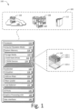
- Fig. 1 illustrates an example operating environment 100 having a host device 102, capable of storing or accessing various forms of data, files, objects, or information.
- a host device 102 may include a computing cluster 104 (e.g., of a cloud 106), a server 108 or server hardware of a data center 110, or a server 112 (e.g., standalone), any of which may be configured as part of a storage network, storage service, or cloud system.
- host device 102 may include a tablet computer, a set-top-box, a data storage appliance, wearable smart-device, television, content-streaming device, high-definition multimedia interface (HDMI) media stick, smart appliance, home automation controller, smart thermostat, Internet-of-Things (IoT) device, mobile-internet device (MID), a network-attached-storage (NAS) drive, aggregate storage system, server blade, gaming console, automotive entertainment device, automotive computing system, automotive control module (e.g., engine or power train control module), and so on.
- HDMI high-definition multimedia interface
- IoT Internet-of-Things
- MID mobile-internet device
- NAS network-attached-storage
- the host device 102 may communicate or store data for any suitable purpose, such as to enable functionalities of a particular type of device, provide a user interface, enable network access, implement gaming applications, playback media, provide navigation, edit content, provide data storage, or the like.
- the host device 102 includes a processor 114 and computer-readable storage media 116.
- the processor 114 may be implemented as any suitable type or number of processors (e.g., x86 or ARM), either single-core or multi-core, for executing instructions or commands of an operating system or other programs of the host device 102.
- the computer-readable media 116 (CRM 116) includes system memory 118 and storage media 120.
- the system memory 118 of the host device 102 may include any suitable type or combination of volatile memory or non-volatile memory.
- the volatile memory of host device 102 may include various types of random-access memory (RAM), dynamic RAM (DRAM), static RAM (SRAM) or the like.
- the non-volatile memory may include read-only memory (ROM), electronically erasable programmable ROM (EEPROM) or Flash memory ( e . g ., NOR Flash or NAND Flash). These memories, individually or in combination, may store data associated with applications, tenants, workloads, initiators, virtual machines, and/or an operating system of host device 102.
- ROM read-only memory
- EEPROM electronically erasable programmable ROM
- Flash memory e . g ., NOR Flash or NAND Flash.
- the storage media 120 of the host device 102 may be configured as any suitable type of data storage media, such as a storage device, storage drive, storage array, storage volume, or the like. Although described with reference to the host device 102, the storage media 120 may also be implemented separately as a standalone device or as part of a larger storage collective, such as a data center, server farm, or virtualized storage system ( e . g ., for cloud-based storage or services). Examples of the storage media 120 include a hard-disk drive (HDD, not shown), an optical-disk drive (not shown), a solid-state drive 122 (SSD 122), and/or an SSD array of SSDs 122-1 through 122-n as shown in Fig. 1 , where n is any suitable integer or number of SSDs.
- HDD hard-disk drive
- SSD 122 solid-state drive
- Each of the SSDs 122 includes or is formed from non-volatile memory devices 124 (NVM devices 124) on which data or information of the host device 102 or other sources is stored.
- the NVM devices 124 may be implemented with any type or combination of solid-state memory media, such Flash, NAND Flash, NAND memory, RAM, DRAM ( e . g ., for caching), SRAM, or the like.
- the data stored to the NVM devices 124 may be organized into files of data ( e . g ., content) or data objects that are stored to the SSDs 122 and accessed by the host device 102 or tenants, workloads, or initiators of the host device.
- the types, sizes, or formats of the files may vary depending on a respective source, use, or application associated with the file.
- the files stored to the SSDs 122 may include audio files, video files, text files, image files, multimedia files, spreadsheets, and so on.
- the host device 102 includes a storage media accelerator 126 (accelerator 126) capable of implementing aspects of virtualizing isolation areas of solid-state storage media.
- the accelerator 126 includes a virtualizer 128, address maps 130, a wear leveler 132, and a load balancer 134, each of which may be implemented to perform respective operations or functions associated with virtualizing isolation areas of solid-state storage media.
- the virtualizer 128 may determine a geometry of solid-state storage media and select, based on the geometry, an area of the solid-state storage media or an isolated unit of storage. The virtualizer 128 may then associate, in the address maps 130, a physical address of area selected for the isolated unit of storage to a virtual address through which the isolated unit of storage is accessible.
- the isolated unit of storage is then exposed by the virtualizer 128, via the virtual address, through a host interface to enable host access of the isolated unit of storage in the solid-state storage media.
- the wear leveler 132 or load balancer 134 remaps the isolated unit of storage to other areas of the solid-state storage media without host interaction (e.g. , notification, interruption, or use of host processing/memory resources).
- the wear leveler 132 may dynamically implement a coarse wear leveling across the solid-state memory devices of a drive, or the load balancer 134 may redistribute highly accessed virtual units of isolated storage to completely different SSDs to implement performance-based load balancing without involving the host system. How these entities are implemented and used varies and is described throughout this disclosure.
- the host device 102 may also include I/O ports 136, a graphics processing unit 138 (GPU 138), and data interfaces 140.
- the I/O ports 136 allow a host device 102 to interact with other devices, peripherals, or users.
- the I/O ports 136 may include or be coupled with a universal serial bus, human interface devices, audio inputs, audio outputs, or the like.
- the GPU 138 processes and renders graphics-related data for host device 102, such as user interface elements of an operating system, applications, or the like. In some cases, the GPU 138 accesses a portion of local memory to render graphics or includes dedicated memory for rendering graphics ( e . g ., video RAM) of the host device 102.
- the data interfaces 140 of the host device 102 provide connectivity to one or more networks and other devices connected to those networks.
- the data interfaces 140 may include wired interfaces, such as Ethernet or fiber optic interfaces for communicating over a local network, intranet, or the Internet.
- the data interfaces 140 may include wireless interfaces that facilitate communication over wireless networks, such as wireless LANs, wide-area wireless networks ( e . g ., cellular networks), and/or wireless personal-area-networks (WPANs). Any of the data communicated through the I/O ports 136 or the data interfaces 140 may be written to or read from the storage media 120 of the host device 102 in accordance with one or more aspects virtualizing isolation areas of solid-state storage media.
- Fig. 2 illustrates example configurations of a storage media accelerator 126 and SSD 122 generally at 200, which are implemented in accordance with one or more aspects of virtualizing isolation areas of solid-state storage media.
- the accelerator 126 is operably coupled between a host 202 and the SSD 122 from which virtualized areas of isolated storage are provided.
- the host 202 includes software 204, such as applications, virtual machines, or tenants (not shown), that execute on compute resources 206 of the host.
- the compute resources 206 include a combination of processing resources and system memory of the host 202 that are used to implement the applications, virtual machines, tenants, or initiators.
- the accelerator 126 may provide isolated access to virtualized units of storage to each virtual machine, tenant, or initiator, while offloading lower-level storage media functions from the compute resources 206.
- the tenants or initiators of the host 202 access data stored in the SSD 122 coupled to the accelerator 126.
- the SSD 122 is implemented with an SSD controller 208 through which channels 210-1 through 120-m of NAND are accessible.
- Each channel 210 of NAND (e.g., channel A or NAND channel 210) includes multiple NAND devices 212-1 through 212-n, which may be implemented as separate NAND devices or NAND dies of the SSD 122 that are accessible or addressable through a respective NAND channel 210.
- the accelerator 126 may select any NAND device 212 or NAND channel 210 for virtualization.
- the accelerator 126 may map a physical NAND device 212 to a virtual storage unit address in the address maps 130.
- the virtual storage unit, or virtual unit of storage, is then exposed by the accelerator 126 to the host 202, such as to a virtual machine or tenant application of the host 202.
- the accelerator 126 may provide isolated storage to the virtual machine or tenant that is isolated from other applications, virtual machines, initiators, or tenants of the host 202.
- Fig. 3 illustrates an example configuration of a storage media accelerator 126 and an array of n SSDs 122 generally at 300, which are implemented in accordance with one or more aspects of virtualizing isolation areas of solid-state storage media.
- the accelerator 126 is operably coupled between a host 302 and an array of SSDs 112-1 through 122-n from which virtualized areas of isolated storage are provided.
- the host 302 may be implemented as a multi-tenant host with virtual machines 304, which may be implemented with any suitable number of virtual machines 304-1 through 304-m.
- the virtual machines 304 execute from a hypervisor 306 that executes on the compute resources 308 of the host 302.
- the compute resources 308 may include a combination of processing resources and system memory of the host 302 that are used to implement the virtual machines 304 through which tenants or initiators operate.
- the accelerator 126 may provide isolated access to virtualized units of storage to each virtual machine 304-1 through 304-m, tenant, or initiator, while offloading lower-level storage media functions from the compute resources 308 of the host 302.
- each SSD 122 of the SSD array is implemented with an SSD controller 208 by which four channels 210 of NAND (e . g ., A-D or E-H) are accessible.
- Each channel 210 of NAND (e . g ., channel E or NAND channel 210-5) includes multiple NAND devices or NAND dies.
- the accelerator 126 may select any SSD 122, NAND channel 210, or NAND devices as a storage area for virtualization.
- the accelerator 126 may map SSD 122-1 to a virtual storage unit address in the address maps 130.
- the virtual storage unit, or virtual unit of storage, is then exposed by the accelerator 126 to the host 302, such as to a virtual machine 304 or tenant application of the host 302.
- the accelerator 126 may provide isolated storage to the virtual machine 304 or tenant that is isolated from other applications, virtual machines 304, initiators, or tenants of the host 302.
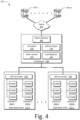
- Fig. 4 illustrates an example configuration of a Fabric-enabled storage media accelerator generally at 400, which is implemented in accordance with one or more aspects of virtualizing isolation areas of solid-state storage media.
- the accelerator 126 includes a Fabric interface (402) and is operably coupled between an instance of a Fabric 404 and an array of SSDs 122-1 through 122-n.
- the Fabric interface 402 may include an NVM over Fabric (NVM-OF) interface, such as a Non-Volatile Memory Express (NVMe) over Ethernet, InfiniBand, or Fibre Channel (FC) interface.
- NVM-OF NVM over Fabric
- NVMe Non-Volatile Memory Express
- FC Fibre Channel
- the accelerator 126 may be implemented as a Fabric-enabled storage target in a disaggregated storage system.
- any of the multiple host devices 102-1 though 102-m may access the SSD 122 array through the accelerator 126.
- each SSD 122 of the SSD array is implemented with an SSD controller 208 by which four channels 210 of NAND (e.g. , A-D or E-H) are accessible.
- Each channel 210 of NAND e.g. , channel E or NAND channel 210-5) includes multiple NAND devices or NAND dies.
- the accelerator 126 may select any SSD 122, NAND channel 210, or NAND devices as a storage area for virtualization.
- the accelerator 126 may map SSD 122-1 to a virtual storage unit address in the address maps 130.
- the virtual storage unit, or virtual unit of storage, is then exposed by the accelerator 126 to the host device 102, such as to a virtual machine or tenant application of one of the host devices 102.
- the accelerator 126 may provide isolated storage to the virtual machine or tenant that is isolated from other host devices, applications, virtual machines, initiators, or tenants.
- the following discussion describes techniques of virtualizing isolation areas of solid-state storage media, which may provide storage isolation and partition functionalities to a host while offloading lower-level storage media functions, such as wear leveling, load balancing, or the like, to a storage media accelerator.
- These techniques may be implemented using any of the environments and entities described herein, such as the accelerator 126, virtualizer 128, address maps 130, wear leveler 132, or load balancer 134.
- These techniques include methods illustrated in Fig. 5 , Fig. 6 , Fig. 8 , and Fig. 10 each of which is shown as a set of operations performed by one or more entities.
- Fig. 5 depicts an example method 500 for virtualizing isolation areas of solid-state storage media, including operations performed by or with the accelerator 126, virtualizer 128, address maps 130, wear leveler 132, or load balancer 134.
- an accelerator determines, via a storage interface, a geometry of solid-state storage media.
- the solid-state storage media may expose the geometry to the accelerator, such as through an open-channel SSD or project Denali compliant interface.
- the geometry includes an architecture, topology, configuration, available control features, or other parameters of a drive in which the solid-state storage media is implemented.
- the geometry of the solid-state storage media may include a logical geometry, a physical geometry, a number of channels, a number of logical units, a number of parallel units, a number of chunks, a chunk size, or a minimum write size of the solid-state storage media.
- the accelerator selects, based on the geometry of the solid-state media, an area of the solid-state storage media as an isolated unit of storage.
- the area selected as the isolated unit of storage may include any granularity or subdivision of solid-state storage, such as an entire SSD, a memory channel of a SSD, a memory device of a SSD, or a memory die of a SSD.
- the accelerator maps a physical address of the area selected for the isolated unit of storage to a virtual address through which the isolated unit of storage is accessible.
- the accelerator may maintain this mapping, as well as other mappings of physical to virtual addresses for isolated units of storage. By so doing, the address mapping function can be offloaded from a host or handled by the accelerator outside of a SSD or SSD controller.
- the accelerator exposes, via the virtual address, the isolated unit of storage through a host interface to enable host access of the isolated unit of storage in the solid-state storage media.
- the isolated unit of storage is associated with an initiator, a workload, a virtual machine, or a tenant of the host. In such cases, the isolated unit of storage is isolated from another initiator, another workload, another virtual machine, or another tenant of the host.
- the solid-state storage media may be configured as nearline or direct attached storage of a host device.
- the accelerator alters the physical address to which the virtual address of the isolated unit of storage is mapped. This may be effective to remap the isolated unit of storage to a different area of the solid-state storage media. In some cases, the physical address is remapped to another area of a SSD as part of a wear leveling function or algorithm. In other cases, the physical address is remapped to another SSD as part of a load balancing function or algorithm implemented by the accelerator.
- Fig. 6 depicts an example method 600 for remapping an isolated unit of storage to another area of storage media in a SSD.
- the operations of method 600 may be performed by or with the accelerator 126, virtualizer 128, address maps 130, wear leveler 132, or load balancer 134.
- an accelerator exposes, via respective virtual addresses, one or more isolated units of storage of a SSD to a host through a host interface.
- the virtualized isolated units of storage may correspond to a NAND channel of a SSD, a NAND device of a SSD, or a NAND die of a SSD.
- NAND channel A is exposed to the host device as a unit of isolated storage.
- a tenant or workload of the host device may access the NAND channel A as isolated storage without conflicting traffic from other tenants or initiators.
- the accelerator monitors use of areas of storage media in the SSD that correspond to the one or more isolated units of storage of the SSD.
- a wear leveler of the accelerator monitors use or access of NAND channels, NAND devices, or NAND dies of the SSD to which the isolated units of storage correspond.
- the tenant of the host device accesses NAND channel A more than other areas of the SSD are accessed.
- the accelerator selects, based on the monitored use, one of the isolated units of storage for remapping to another area of storage media in the SSD. For example, the accelerator may select an isolated unit of storage that corresponds to a heavily a used NAND channel, NAND device, of NAND die of the SSD for remapping. As described herein, the accelerator may remap virtualized isolation areas without host interaction or use of host resources. Continuing the ongoing example, the accelerator selects NAND channel A for remapping to another area of the SSD.
- the accelerator remaps a physical address of the another area of storage media to the respective virtual address of the isolated unit of storage.
- the accelerator may dynamically implement wear leveling by redirecting access to the another area of storage media.
- the accelerator remaps a physical address for the tenant's isolated unit of storage from NAND channel A to NAND channel D of the SSD.
- the accelerator exposes, via the respective virtual address, the remapped isolated unit of storage to the host through the host interface. This may be effective to enable host access to the another area of storage media in the SSD through the virtual address of the isolated unit of storage. Due to the virtual addressing of the isolated unit of storage, the remapping is transparent to the host or tenant, and also requires no host interaction or resources due to offloading provided by the accelerator. Concluding the present example, the accelerator migrates data from NAND channel A to NAND channel D in the SSD and redirects, via the virtual address, access by the tenant of the host device to NAND channel D for subsequent data access.
- the accelerator erases the area of storage media in the SSD to which the virtual address of the remapped isolated unit of storage was previously mapped. This may be effective to free the area of storage media for reallocation or reuse with another isolated unit of storage in the SSD.
- Fig. 8 depicts an example method 800 for remapping an isolated unit of storage to another SSD, including operations performed by or with the accelerator 126, virtualizer 128, address maps 130, wear leveler 132, or load balancer 134.
- an accelerator exposes, via respective virtual addresses, one or more isolated units of storage in solid-state storage media to a host through a host interface.
- the virtualized isolated units of storage may correspond to a SSD, a NAND channel of a SSD, a NAND device of a SSD, or a NAND die of a SSD.
- NAND channel A of a first SSD of a SSD array is exposed to the host device as a unit of isolated storage.
- a tenant or workload of the host device may access the NAND channel A as isolated storage without conflicting traffic from other tenants or initiators.
- the accelerator monitors use of areas of storage media in the solid-state storage media that correspond to the one or more isolated units of storage.
- a load balancer of the accelerator monitors use or access between SSDs or respective areas of SSDs to which the isolated units of storage correspond.
- the tenant of the host device accesses NAND channel A of the SSD 122-1 more than other SSDs in the array are accessed.
- the accelerator selects, based on the monitored use, one of the isolated units of storage for remapping to another area of storage media in the solid-state storage media. For example, the accelerator may select an isolated unit of storage that corresponds to a heavily used or accessed SSD for remapping. As described herein, the accelerator may remap virtualized isolation areas to different SSDs without host interaction or use of host resources. Continuing the ongoing example, the accelerator selects SSD 122-1 for remapping to another SSD of the array.
- the accelerator remaps a physical address of the another area of storage media to the respective virtual address of the isolated unit of storage.
- the accelerator may dynamically implement load balancing by redirecting access to the another area of storage media.
- the accelerator remaps a physical address for the tenant's isolated unit of storage from NAND channel A of SSD 122-1 to NAND channel E of the SSD 122-n in the array.
- the accelerator exposes, via the respective virtual address, the remapped isolated unit of storage to the host through the host interface. This may be effective to enable host access to the another area of storage media in the solid-state storage media through the virtual address of the isolated unit of storage. Concluding the present example, the accelerator migrates data from NAND channel A of SSD 122-1 to NAND channel E of SSD 122-n and redirects, via the virtual address, access by the tenant of the host device from SSD 122-1 to SSD 122-n for subsequent data access.
- the accelerator erases the area of storage media in the solid-state storage media to which the virtual address of the remapped isolated unit of storage was previously mapped. This may be effective to free the area of storage media for reallocation or reuse with another isolated unit of storage in the solid-state storage media.
- the accelerator may erase a SSD, a NAND channel, a NAND device, or a NAND die of data to clear the storage area.
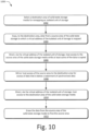
- Fig. 10 depicts an example method 1000 for migrating data of a virtualized isolation area from a source area of storage media to a destination area of storage media.
- the operations of method 1000 may be performed by or with the accelerator 126, virtualizer 128, address maps 130, wear leveler 132, or load balancer 134.
- an accelerator selects a destination area of solid-state storage media for remapping an isolated unit of storage.
- the destination area may include an entire SSD, a NAND channel of a SSD, or a NAND device of a SSD.
- the accelerator copies, to the destination area, data from a source area of solid-state storage media to which a virtual address of the isolated unit of storage is mapped.
- the accelerator directs, via the virtual address of the isolated unit of storage, host access to the source area of the solid-state storage media while at least some of the data is copied.
- the accelerator may copy data from an active isolation unit of storage to a spare unit while at least some read/write access continues to be directed to the active isolation unit of storage.
- the accelerator mirrors host access of the source area to the destination area for access of data that is below a watermark of synchronized data.
- new writes to the active isolation unit that are directed below a watermark of data already copied to the spare isolation unit may be mirrored to both units for data coherency during the migration.
- the accelerator directs, via the virtual address of the isolated unit of storage, host access to the destination area of the solid-state storage media. Responsive to synchronization between the active isolation unit of storage and the destination area, the accelerator may redirect access made through the virtual address to the new unit of storage where the copied data resides. Optionally at 1012, the accelerator erases the data from the source area of the solid-state media to free the source area.
- Fig. 11 illustrates an exemplary System-on-Chip (SoC) 1100 that may implement various aspects of virtualizing isolation areas of solid-state storage media.
- the SoC 1100 may be implemented in any suitable device, such as a computing device, host device, network-attached storage, smart appliance, printer, set-top box, server, data center, solid-state drive (SSD), storage drive array, memory module, automotive computing system, server, server blade, storage blade, storage backplane, storage media expansion device, storage media card, storage media adapter, network attached storage, Fabric-enabled storage target, NVMe-based storage controller, or any other suitable type of device (e.g., others described herein).
- SSD solid-state drive
- ASIC application-specific integrated-circuit
- ASSP application-specific standard product
- DSP digital signal processor
- PSoC programmable SoC
- SiP system-in-package
- FPGA field-programmable gate array
- the SoC 1100 may be integrated with electronic circuitry, a microprocessor, memory, input-output (I/O) control logic, communication interfaces, firmware, and/or software useful to provide functionalities of a host device or storage system, such as any of the devices or components described herein (e.g., storage drive or storage array).
- the SoC 1100 may also include an integrated data bus or interconnect fabric (not shown) that couples the various components of the SoC for data communication or routing between the components.
- the integrated data bus, interconnect fabric, or other components of the SoC 1100 may be exposed or accessed through an external port, parallel data interface, serial data interface, peripheral component interface, or any other suitable data interface.
- the components the SoC 1100 may access or control external storage media through an external interface or off-chip data interface.
- the SoC 1100 includes various components such as input-output (I/O) control logic 1102 and a hardware-based processor 1104 (processor 1104), such as a microprocessor, processor core, application processor, DSP, or the like (e.g., processing resource separate from a host x86 processor).
- the SoC 1100 also includes memory 1106, which may include any type and/or combination of RAM, SRAM, DRAM, non-volatile memory, ROM, one-time programmable (OTP) memory, multiple-time programmable (MTP) memory, Flash memory, and/or other suitable electronic data storage.
- the processor 1104 and code stored on the memory 1106 are implemented as a storage media accelerator or accelerator-enabled storage aggregator to provide various functionalities associated with virtualizing isolation areas of solid-state storage media.
- the memory 1106 stores data, code, instructions, or other information via non-transitory signals, and does not include carrier waves or transitory signals.
- SoC 1100 may comprise a data interface (not shown) for accessing additional or expandable off-chip storage media, such as magnetic memory or solid-state memory ( e . g ., Flash or NAND memory).
- the SoC 1100 may also include firmware 1108, applications, programs, software, and/or operating systems, which may be embodied as processor-executable instructions maintained on the memory 1106 for execution by the processor 1104 to implement functionalities of the SoC 1100.
- the SoC 1100 may also include other communication interfaces, such as a transceiver interface for controlling or communicating with components of a local on-chip (not shown) or off-chip communication transceiver.
- the transceiver interface may also include or implement a signal interface to communicate radio frequency (RF), intermediate frequency (IF), or baseband frequency signals off-chip to facilitate wired or wireless communication through transceivers, physical layer transceivers (PHYs), or media access controllers (MACs) coupled to the SoC 1100.
- the SoC 1100 may include a transceiver interface configured to enable storage over a wired or wireless network, such as to provide a network attached storage (NAS) volume with virtualized storage isolation features.
- NAS network attached storage
- the SoC 1100 also includes an accelerator 126 with a virtualizer 128, address maps 130, wear leveler 132, and load balancer 134, which may be implemented separately as shown or combined with a storage component or data interface.
- the accelerator 126 may expose virtualized units of storage to a host or tenants and offload other storage media management functions to the processor 1104 of the accelerator, such as wear leveling, load balancing, or the like.
- the address maps 130 may be stored on the memory 1106 of the SoC 1100 or on a memory operably coupled with the SoC 1100 and accessible to the accelerator 126.
- any of these entities may be embodied as disparate or combined components, as described with reference to various aspects presented herein. Examples of these components and/or entities, or corresponding functionality, are described with reference to the respective components or entities of the environment 100 of Fig. 1 or respective configurations illustrated in Fig. 2 , Fig. 3 , and/or Fig. 4 .
- the accelerator 126 may be implemented as processor-executable instructions maintained by the memory 1106 and executed by the processor 1104 to implement various aspects and/or features of virtualizing isolation areas of solid-state storage media.
- the accelerator 126 may be implemented independently or in combination with any suitable component or circuitry to implement aspects described herein.
- accelerator 126 may be implemented as part of a DSP, processor/storage bridge, I/O bridge, graphics processing unit, memory controller, storage controller, arithmetic logic unit (ALD), or the like.
- the accelerator 126 may also be provided integrally with other entities of SoC 1100, such as integrated with the processor 1104, memory 1106, a host interface, a storage media interface, or firmware 1108 of the SoC 1100.
- the accelerator 126, virtualizer 128, wear leveler 132, load balancer 134, and/or other components of the SoC 1100 may be implemented as hardware, firmware, fixed logic circuitry, or any combination thereof.
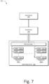
- Fig. 12 illustrates an example storage media accelerator 1200 in accordance with one or more aspects of virtualizing isolation areas of solid-state storage media.
- the storage media accelerator 1200 or any combination of components thereof may be implemented as a storage drive controller, storage media controller, NAS controller, Fabric interface, NVMe initiator, NVMe target, or a storage aggregation controller for solid-state storage media.
- the storage media accelerator 1200 is implemented similar to or with components of the SoC 1100 as described with reference to Fig. 11 .
- an instance of the SoC 1100 may be configured as a storage media accelerator, such as the storage media accelerator 1200 to provide and manage virtualized isolation areas of solid-state media.
- the storage media accelerator 1200 includes input-output (I/O) control logic 1202 and a processor 1204, such as a microprocessor, processor core, application processor, DSP, or the like.
- processor 1204 and firmware of the storage media accelerator 1200 may be implemented to provide various functionalities associated with virtualizing isolation areas of solid-state storage media, such as those described with reference to methods 500, 600, 800, and/or 1000.
- the storage media accelerator also includes a storage media interface 1206 and a host interface 1208, which enable access to storage media and host system, respectively.
- the storage media interface 1206 may include a physical page addressing (PPA) interface, peripheral component interconnect express (PCIe) interface, non-volatile memory express (NVMe) interface, NVM over Fabric (NVM-OF) interface, NVM host controller interface specification (NVMHCIS) compliant interface, or the like.
- PPA physical page addressing
- PCIe peripheral component interconnect express
- NVMe non-volatile memory express
- NVM-OF NVM over Fabric
- NVMHCIS NVM host controller interface specification
- the host interface may include a PCIe interface, SATA-based interface, NVMe interface, NVM-OF interface, NVMHCIS compliant interface, Fabric-enabled storage interface, or the like.
- the storage media accelerator 1200 includes a flash translation layer 1210 (FTL 1210) and a garbage collector 1212.
- FTL 1210 flash translation layer 1210
- garbage collector 1212 for managing access of storage media of SSDs that are operably coupled with the accelerator.
- the FTL 1210 may include a log manager for managing sequential write streams (e.g., write buffering), maintaining address maps of storage media, and implementing or coordinating garbage collection or media reuse with the garbage collector 1212.
- the FTL 1210 may include a media management module for wear leveling, error correction coding, read-retry, bad-block management, metadata recovery, or the like.
- these SSD functionalities may also be implemented by or offloaded to the storage media accelerator 1200.
- the storage media accelerator 1200 also includes instances of a virtualizer 128, address maps 130, wear leveler 132, and load balancer 134. Any or all of these components may be implemented separately as shown or combined with the processor 1204, storage media interface 1206, host interface 1208, or flash translation layer 1210. Examples of these components and/or entities, or corresponding functionality, are described with reference to the respective components or entities of the environment 100 of Fig. 1 or respective configurations illustrated in Fig. 2 , Fig. 3 , and/or Fig. 4 .
- the storage media accelerator 1200 either in whole or part, may be implemented as processor-executable instructions maintained by memory (not shown) of the accelerator and executed by the processor 1204 to implement various aspects and/or features of virtualizing isolation areas of solid-state storage media.
Landscapes
- Engineering & Computer Science (AREA)
- Theoretical Computer Science (AREA)
- Physics & Mathematics (AREA)
- General Engineering & Computer Science (AREA)
- General Physics & Mathematics (AREA)
- Human Computer Interaction (AREA)
- Software Systems (AREA)
- Computer Networks & Wireless Communication (AREA)
- Information Retrieval, Db Structures And Fs Structures Therefor (AREA)
- Memory System Of A Hierarchy Structure (AREA)
- Hall/Mr Elements (AREA)
- Mram Or Spin Memory Techniques (AREA)
- Developing Agents For Electrophotography (AREA)
- Memory System (AREA)
- Debugging And Monitoring (AREA)
- Storage Device Security (AREA)
Claims (13)
- Verfahren zur Virtualisierung von Isolationsbereichen von Festkörperspeichermedien, wobei das Verfahren von einem Speichermedienbeschleuniger durchgeführt wird, der mit einer Host-schnittstelle gekoppelt ist, wobei das Verfahren umfasst:Bestimmen einer Geometrie eines mit der Speichermedienschnittstelle gekoppelten Solid-State-Speichermedienlaufwerks über eine von dem Speichermedienbeschleuniger bereitgestellte Speichermedienschnittstelle, wobei die Geometrie mehrere Kanäle von Solid-State-Speichermedien des Solid-State-Speichermedienlaufwerks umfasst, wobei jeder der mehreren Kanäle den Zugriff auf jeweilige Solid-State-Speichermedienchips des Solid-State-Speichermedienlaufwerks ermöglicht, die mit dem Kanal von Solid-State-Speichermedien gekoppelt sind;Auswählen, basierend auf der Geometrie des Solid-State-Speichermedien-Laufwerks, eines der mehreren Kanäle der Solid-State-Speichermedien des Solid-State-Speichermedien-Laufwerks als eine isolierte Speichereinheit, wobei die isolierte Speichereinheit alle der jeweiligen Solid-State-Speichermedien-Chips umfasst, die mit dem Kanal der Solid-State-Speichermedien des Solid-State-Speichermedien-Laufwerks verbunden sind;Abbilden einer physikalischen Adresse der isolierten Speichereinheit, die den Kanal der Solid-State-Speichermedien umfasst, auf eine virtuelle Adresse, über die die isolierte Speichereinheit zugänglich ist;dadurch gekennzeichnet, dass das Verfahren ferner Folgendes umfasst:Freigeben der isolierten Speichereinheit über die virtuelle Adresse durch die Hostschnittstelle, um einem Initiator, der auf einem Host ausgeführt wird, den Zugriff auf die jeweiligen Solid-State-Speicherchips des Kanals der Solid-State-Speichermedien als isolierte Speichereinheit in dem Solid-State-Speichermedienlaufwerk zu ermöglichen,wobei alle jeweiligen Solid-State-Speichermedien-Chips des Kanals der Solid-State-Speichermedien, die die isolierte Speichereinheit bilden, vom Speicherverkehr von anderen Tenants, die auf dem Host ausgeführt werden, isoliert sind.
- Das Verfahren nach Anspruch 1, wobei das Solid-State-Speichermedien-Laufwerk ein erstes Solid-State-Speichermedien-Laufwerk ist und das Verfahren ferner umfasst, dass auf der Grundlage der Geometrie des ersten Solid-State-Speichermedien-Laufwerks oder eines zweiten Solid-State-Speichermedien-Laufwerks die physikalische Adresse geändert wird, auf die die virtuelle Adresse der isolierten Speichereinheit abgebildet wird, um die isolierte Speichereinheit auf einen anderen der mehreren Kanäle von Solid-State-Speichermedien des ersten Solid-State-Speichermedien-Laufwerks oder auf einen der mehreren Kanäle von Solid-State-Speichermedien des zweiten Solid-State-Speichermedien-Laufwerks umzubuchen.
- Das Verfahren nach Anspruch 2, wobei das erste Solid-State-Speichermedien-Laufwerk ein erstes Solid-State-Laufwerk, SSD, ist, das zweite Solid-State-Speichermedien-Laufwerk ein zweites SSD ist, die physikalische Adresse eine erste physikalische Adresse ist, der Kanal der Solid-State-Speichermedien des ersten SSD ein erster Kanal der Solid-State-Speichermedien ist, der andere der mehreren Kanäle der Solid-State-Speichermedien des ersten SSD oder der Kanal der Solid-State-Speichermedien des zweiten SSD einen zweiten Kanal der Solid-State-Speichermedien umfasst, und das Ändern der ersten physikalischen Adresse einen der folgenden Schritte umfasst:Abbilden einer zweiten physikalischen Adresse des zweiten Kanals von Festkörperspeichermedien, der sich in dem Festkörperspeichermedienlaufwerk der ersten SSD befindet, auf die virtuelle Adresse der isolierten Speichereinheit; oderAbbildung einer zweiten physikalischen Adresse des zweiten Kanals von Solid-State-Speichermedien, der sich im Solid-State-Speichermedienlaufwerk der zweiten SSD befindet, auf die virtuelle Adresse der isolierten Speichereinheit.
- Das Verfahren nach Anspruch 3, wobei:die Abbildung der zweiten physikalischen Adresse des zweiten Kanals der Festkörperspeichermedien der ersten SSD auf die virtuelle Adresse als Teil einer Verschleißausgleichsfunktion implementiert wird; oderdie Abbildung der zweiten physikalischen Adresse des zweiten Kanals der Solid-State-Speichermedien der zweiten SSD auf die virtuelle Adresse als Teil einer Lastausgleichsfunktion implementiert wird.
- Das Verfahren nach einem der Ansprüche 1 bis 4, wobei die Geometrie des Festkörperspeichermediums mindestens eine logische Geometrie, eine physikalische Geometrie, eine Anzahl von Kanälen, eine Anzahl von logischen Einheiten, eine Anzahl von parallelen Einheiten, eine Anzahl von Chunks, eine Chunk-Größe oder eine minimale Schreibgröße des Festkörperspeichermediums umfasst.
- Das Verfahren nach einem der Ansprüche 1 bis 5, wobei:die Speichermedienschnittstelle eine physikalische Seitenadressierungs-, PPA-, Schnittstelle, eine Peripheral Component Interconnect Express-, PCIe-, Schnittstelle, eine Non-Volatile Memory Express-, NVMe-, Schnittstelle, eine NVM over Fabric-, NVM-OF-, Schnittstelle oder eine NVM Host Controller interface Specification-, NVMHCIS-, konforme Schnittstelle umfasst; unddie Host-Schnittstelle eine PCIe-Schnittstelle, eine NVMe-Schnittstelle, eine NVM-OF-Schnittstelle oder eine NVMHCIS-konforme Schnittstelle umfasst.
- Eine Vorrichtung, die Folgendes umfasst:einen hardwarebasierten Prozessor;einen Speicher, der mit dem Prozessor gekoppelt und so konfiguriert ist, dass er prozessorausführbare Anweisungen enthält, die als Reaktion auf die Ausführung eine Anwendung auf dem Gerät implementieren;eine Host-Schnittstelle, die so konfiguriert ist, dass die Anwendung auf Daten in Speichermedien zugreifen kann, die der Vorrichtung zugeordnet sind;einen Speichermedienbeschleuniger, der mit der Hostschnittstelle gekoppelt ist und eine Speichermedienschnittstelle bereitstellt, wobei der Speichermedienbeschleuniger konfiguriert ist, um:Bestimmen, durch die Speichermedienschnittstelle, einer Geometrie eines Festkörperspeichermedienlaufwerks, das betriebsfähig mit der Vorrichtung gekoppelt ist, wobei die Geometrie mehrere Kanäle von Festkörperspeichermedien des Festkörperspeichermedienlaufwerks umfasst, wobei jeder der mehreren Kanäle den Zugriff auf entsprechende Festkörperspeichermedienchips des Festkörperspeichermedienlaufwerks ermöglicht, die mit dem Kanal von Festkörperspeichermedien gekoppelt sind;Auswählen, basierend auf der Geometrie des Solid-State-Speichermedien-Laufwerks, eines der mehreren Kanäle der Solid-State-Speichermedien des Solid-State-Speichermedien-Laufwerks als eine isolierte Speichereinheit, wobei die isolierte Speichereinheit alle der jeweiligen Solid-State-Speichermedien-Chips umfasst, die mit dem Kanal der Solid-State-Speichermedien des Solid-State-Speichermedien-Laufwerks verbunden sind;Abbilden einer physikalischen Adresse der isolierten Speichereinheit, die den Kanal der Festkörperspeichermedien umfasst, auf eine virtuelle Adresse, über die die isolierte Speichereinheit zugänglich ist;dadurch gekennzeichnet, dass der Speichermedienbeschleuniger ferner konfiguriert ist, um:die isolierte Speichereinheit über die virtuelle Adresse durch die Hostschnittstelle freizugeben, um einem Initiator, der auf einem Host ausgeführt wird, den Zugriff auf die isolierte Speichereinheit in dem Solid-State-Speichermedienlaufwerk durch die Anwendung zu ermöglichen,wobei alle jeweiligen Festkörperspeichermedienwürfel des Kanals von Festkörperspeichermedien, die die isolierte Speichereinheit bilden, vom Speicherverkehr von anderen Tenants, die auf dem Host ausgeführt werden, isoliert sind.
- Die Vorrichtung nach Anspruch 7, wobei das Solid-State-Speichermedienlaufwerk ein erstes Solid-State-Speichermedienlaufwerk ist und der Speichermedienbeschleuniger ferner implementiert ist, um auf der Grundlage der Geometrie des ersten Solid-State-Speichermedienlaufwerks oder eines zweiten Solid-State-Speichermedienlaufwerks die physikalische Adresse, auf die die virtuelle Adresse der isolierten Speichereinheit abgebildet wird, zu ändern, um die isolierte Speichereinheit auf einen anderen der mehreren Kanäle von Solid-State-Speichermedien des ersten Solid-State-Speichermedien-Laufwerks oder auf einen der mehreren Kanäle von Solid-State-Speichermedien des zweiten Solid-State-Speichermedien-Laufwerks umzubilden.
- Die Vorrichtung nach Anspruch 8, wobei das erste Solid-State-Speichermedienlaufwerk ein erstes Solid-State-Laufwerk, SSD, ist, das zweite Solid-State-Speichermedienlaufwerk ein zweites SSD ist, die physikalische Adresse eine erste physikalische Adresse ist, der Kanal der Solid-State-Speichermedien des ersten SSD ein erster Kanal der Solid-State-Speichermedien ist, der andere der mehreren Kanäle der Solid-State-Speichermedien des ersten SSD oder der Kanal der Solid-State-Speichermedien des zweiten SSD einen zweiten Kanal der Solid-State-Speichermedien umfasst, und der Speichermedienbeschleuniger ferner implementiert ist, um:der virtuellen Adresse der isolierten Speichereinheit eine zweite physikalische Adresse des zweiten Kanals von Festkörperspeichermedien zuzuordnen, der sich in dem Festkörperspeichermedienlaufwerk der ersten SSD befindet; oderder virtuellen Adresse der isolierten Speichereinheit eine zweite physikalische Adresse des zweiten Kanals von Festkörperspeichermedien zuzuordnen, die sich im Festkörperspeichermedienlaufwerk der zweiten SSD befindet.
- Die Vorrichtung nach Anspruch 7, wobei:
die Geometrie des Festkörperspeichermedienlaufwerks mindestens eines von einer logischen Geometrie, einer physikalischen Geometrie, einer Anzahl von Kanälen, einer Anzahl von logischen Einheiten, einer Anzahl von parallelen Einheiten, einer Anzahl von Chunks, einer Chunk-Größe oder einer minimalen Schreibgröße des Festkörperspeichermediums umfasst. - Die Vorrichtung nach Anspruch 7, wobei:die Vorrichtung ferner das Festkörperspeichermedienlaufwerk umfasst, das betriebsfähig mit der Speichermedienschnittstelle des Speichermedienbeschleunigers gekoppelt ist; oderdas Festkörperspeichermedienlaufwerk als Nearline- oder direkt angeschlossener Speicher der Vorrichtung konfiguriert ist; oderwobei:die Anwendung eine erste Anwendung ist, die mit der isolierten Speichereinheit verbunden ist;als Reaktion auf die Ausführung implementieren die prozessorausführbaren Anweisungen ferner eine zweite Anwendung auf der Vorrichtung; unddie isolierte Speichereinheit vom Zugriff durch die zweite Anwendung auf dem Gerät isoliert ist.
- Ein System-on-Chip (SoC), umfassend die Vorrichtung nach einem der Ansprüche 7 bis 11.
- Das SoC nach Anspruch 12, wobei das SoC auf einem Host-Gerät, einem Server, einem Server-Blade, einem Storage-Blade, einer Storage-Backplane, einem Speichermedien-Erweiterungsgerät, einer Speichermedien-Karte, einem Speichermedien-Adapter, einem Network Attached Storage, einem Fabric-fähigen Speicherziel oder einem NVMe-basierten Speicher-Controller verkörpert oder als Teil davon implementiert ist.
Applications Claiming Priority (1)
| Application Number | Priority Date | Filing Date | Title |
|---|---|---|---|
| US201862715718P | 2018-08-07 | 2018-08-07 |
Publications (2)
| Publication Number | Publication Date |
|---|---|
| EP3608787A1 EP3608787A1 (de) | 2020-02-12 |
| EP3608787B1 true EP3608787B1 (de) | 2024-10-02 |
Family
ID=67658534
Family Applications (1)
| Application Number | Title | Priority Date | Filing Date |
|---|---|---|---|
| EP19190611.4A Active EP3608787B1 (de) | 2018-08-07 | 2019-08-07 | Virtualisierung von isolationsbereichen von festkörperspeichermedien |
Country Status (4)
| Country | Link |
|---|---|
| US (1) | US11656775B2 (de) |
| EP (1) | EP3608787B1 (de) |
| KR (1) | KR102862882B1 (de) |
| CN (1) | CN110825320B (de) |
Families Citing this family (19)
| Publication number | Priority date | Publication date | Assignee | Title |
|---|---|---|---|---|
| US11074013B2 (en) | 2018-08-07 | 2021-07-27 | Marvell Asia Pte, Ltd. | Apparatus and methods for providing quality of service over a virtual interface for solid-state storage |
| US11010314B2 (en) | 2018-10-30 | 2021-05-18 | Marvell Asia Pte. Ltd. | Artificial intelligence-enabled management of storage media access |
| US11132291B2 (en) * | 2019-01-04 | 2021-09-28 | Alibaba Group Holding Limited | System and method of FPGA-executed flash translation layer in multiple solid state drives |
| US11481118B2 (en) | 2019-01-11 | 2022-10-25 | Marvell Asia Pte, Ltd. | Storage media programming with adaptive write buffer release |
| US10922003B1 (en) * | 2019-09-16 | 2021-02-16 | ScaleFlux, Inc. | Realizing host-assisted device-level data deduplication on solid-state data storage devices with embedded non-volatile memory |
| US11397694B2 (en) | 2019-09-17 | 2022-07-26 | Micron Technology, Inc. | Memory chip connecting a system on a chip and an accelerator chip |
| US11416422B2 (en) | 2019-09-17 | 2022-08-16 | Micron Technology, Inc. | Memory chip having an integrated data mover |
| US11100033B1 (en) * | 2020-04-30 | 2021-08-24 | Dell Products L.P. | Single-root input/output virtualization-based storage solution for software defined storage |
| US11175828B1 (en) * | 2020-05-14 | 2021-11-16 | EMC IP Holding Company LLC | Mitigating IO processing performance impacts in automated seamless migration |
| US11720413B2 (en) * | 2020-06-08 | 2023-08-08 | Samsung Electronics Co., Ltd. | Systems and methods for virtualizing fabric-attached storage devices |
| US12039356B2 (en) * | 2021-01-06 | 2024-07-16 | Baidu Usa Llc | Method for virtual machine migration with checkpoint authentication in virtualization environment |
| CN113342697B (zh) * | 2021-07-19 | 2022-08-26 | 英韧科技(上海)有限公司 | 闪存转换层仿真测试系统及方法 |
| KR20230039127A (ko) | 2021-09-13 | 2023-03-21 | 에스케이하이닉스 주식회사 | Ssd에 포함된 존의 병렬성을 탐지하는 장치 및 그 동작 방법 |
| US12487776B1 (en) | 2021-10-28 | 2025-12-02 | Marvell Israel (M.I.S.L) Ltd. | Method and apparatus for transferring data between a host computer and a solid state memory |
| CN115098407B (zh) * | 2022-06-30 | 2026-03-03 | 山东云海国创云计算装备产业创新中心有限公司 | 一种混合raid构建的方法、系统、设备及介质 |
| KR20240079650A (ko) * | 2022-11-29 | 2024-06-05 | 삼성전자주식회사 | 다이렉트 스토리지 기능을 지원하는 스토리지 장치 및 스토리지 시스템 |
| KR20250012280A (ko) | 2023-07-17 | 2025-01-24 | 삼성전자주식회사 | 스토리지 시스템 및 이를 포함하는 컴퓨팅 시스템 |
| CN118426698B (zh) * | 2024-05-08 | 2025-07-11 | 汇钜存储科技(东莞)有限公司 | 一种闪存单元的数据存储方法、装置、介质及存储设备 |
| CN119847443B (zh) * | 2024-12-31 | 2026-01-06 | 成都芯盛集成电路有限公司 | 一种提高ssd盘内dram利用效率的方法、系统及存储介质 |
Family Cites Families (91)
| Publication number | Priority date | Publication date | Assignee | Title |
|---|---|---|---|---|
| US6671791B1 (en) | 2001-06-15 | 2003-12-30 | Advanced Micro Devices, Inc. | Processor including a translation unit for selectively translating virtual addresses of different sizes using a plurality of paging tables and mapping mechanisms |
| US7433948B2 (en) | 2002-01-23 | 2008-10-07 | Cisco Technology, Inc. | Methods and apparatus for implementing virtualization of storage within a storage area network |
| US7406598B2 (en) | 2004-02-17 | 2008-07-29 | Vixs Systems Inc. | Method and system for secure content distribution |
| EP1755528B1 (de) | 2004-06-15 | 2012-04-25 | DENTSPLY International Inc. | Dentalzusammensetzungen mit geringer schwindung und geringer spannung |
| US7502908B2 (en) | 2006-05-04 | 2009-03-10 | International Business Machines Corporation | Method for providing an address format compatible with different addressing formats used for addressing different sized address spaces |
| US20080100636A1 (en) | 2006-10-31 | 2008-05-01 | Jiin Lai | Systems and Methods for Low-Power Computer Operation |
| US7783858B2 (en) | 2007-01-20 | 2010-08-24 | International Business Machines Corporation | Reducing memory overhead of a page table in a dynamic logical partitioning environment |
| US7861036B2 (en) | 2007-09-18 | 2010-12-28 | Agere Systems Inc. | Double degraded array protection in an integrated network attached storage device |
| US8571745B2 (en) | 2008-04-10 | 2013-10-29 | Robert Todd Pack | Advanced behavior engine |
| JP5186982B2 (ja) | 2008-04-02 | 2013-04-24 | 富士通株式会社 | データ管理方法及びスイッチ装置 |
| US8806101B2 (en) | 2008-12-30 | 2014-08-12 | Intel Corporation | Metaphysical address space for holding lossy metadata in hardware |
| JP4915756B2 (ja) * | 2009-12-16 | 2012-04-11 | インターナショナル・ビジネス・マシーンズ・コーポレーション | アドレス変換を高速化する方法及びシステム |
| US9389895B2 (en) | 2009-12-17 | 2016-07-12 | Microsoft Technology Licensing, Llc | Virtual storage target offload techniques |
| JP5660053B2 (ja) | 2010-01-20 | 2015-01-28 | 日本電気株式会社 | ネットワーク装置、ネットワーク構成方法及びネットワーク装置のプログラムを記録したプログラム記録媒体 |
| US8521812B2 (en) | 2010-09-24 | 2013-08-27 | Pravala Inc. | Accessing local network resources in a multi-interface system |
| US8495274B2 (en) | 2010-12-08 | 2013-07-23 | International Business Machines Corporation | Address translation table to enable access to virtual functions |
| US8726276B2 (en) | 2011-01-26 | 2014-05-13 | International Business Machines Corporation | Resetting a virtual function that is hosted by an input/output adapter |
| WO2012137265A1 (en) | 2011-04-08 | 2012-10-11 | Hitachi, Ltd. | Computer, computer system, and data communication method |
| US8751713B2 (en) | 2011-05-06 | 2014-06-10 | International Business Machines Corporation | Executing virtual functions using memory-based data in a PCI express SR-IOV and MR-IOV environment |
| US9251059B2 (en) * | 2011-09-23 | 2016-02-02 | Avalanche Technology, Inc. | Storage system employing MRAM and redundant array of solid state disk |
| US8954822B2 (en) | 2011-11-18 | 2015-02-10 | Sandisk Enterprise Ip Llc | Data encoder and decoder using memory-specific parity-check matrix |
| US8713562B2 (en) | 2012-01-06 | 2014-04-29 | International Business Machines Corporation | Intelligent and automated code deployment |
| US9015351B1 (en) | 2012-03-02 | 2015-04-21 | Marvell International Ltd. | Address translation for SR-IOV virtual function apertures |
| US9098805B2 (en) | 2012-03-06 | 2015-08-04 | Koodbee, Llc | Prediction processing system and method of use and method of doing business |
| CA2903367A1 (en) | 2012-03-06 | 2013-09-12 | Koodbee, Llc | Prediction processing system and method of use and method of doing business |
| CN102708316B (zh) * | 2012-04-19 | 2015-04-08 | 北京华胜天成科技股份有限公司 | 一种用于多租户架构中数据隔离的方法 |
| US8805990B2 (en) * | 2012-07-12 | 2014-08-12 | Microsoft Corporation | Load balancing for single-address tenants |
| US9836316B2 (en) * | 2012-09-28 | 2017-12-05 | Intel Corporation | Flexible acceleration of code execution |
| US9134779B2 (en) | 2012-11-21 | 2015-09-15 | International Business Machines Corporation | Power distribution management in a system on a chip |
| US9424219B2 (en) | 2013-03-12 | 2016-08-23 | Avago Technologies General Ip (Singapore) Pte. Ltd. | Direct routing between address spaces through a nontransparent peripheral component interconnect express bridge |
| US9720717B2 (en) | 2013-03-14 | 2017-08-01 | Sandisk Technologies Llc | Virtualization support for storage devices |
| CN104050201B (zh) * | 2013-03-15 | 2018-04-13 | 伊姆西公司 | 用于多租户分布式环境中的数据管理的方法和设备 |
| US20150378886A1 (en) | 2013-04-08 | 2015-12-31 | Avalanche Technology, Inc. | Software-defined ssd and system using the same |
| US9734096B2 (en) | 2013-05-06 | 2017-08-15 | Industrial Technology Research Institute | Method and system for single root input/output virtualization virtual functions sharing on multi-hosts |
| US10635316B2 (en) | 2014-03-08 | 2020-04-28 | Diamanti, Inc. | Methods and systems for data storage using solid state drives |
| US9501245B2 (en) | 2014-05-02 | 2016-11-22 | Cavium, Inc. | Systems and methods for NVMe controller virtualization to support multiple virtual machines running on a host |
| CN104202359A (zh) * | 2014-08-12 | 2014-12-10 | 浪潮电子信息产业股份有限公司 | 一种基于刀片服务器的NVMe SSD虚拟化设计方法 |
| KR101579941B1 (ko) * | 2014-09-03 | 2015-12-23 | 서울대학교 산학협력단 | 가상머신 i/o 관리 방법 및 장치 |
| CN104461958B (zh) | 2014-10-31 | 2018-08-21 | 华为技术有限公司 | 支持sr-iov的存储资源访问方法、存储控制器及存储设备 |
| CN105812260B (zh) * | 2014-12-31 | 2019-03-19 | 华为技术有限公司 | 一种控制mac地址转发表发送的方法、装置及系统 |
| US20160218991A1 (en) * | 2015-01-23 | 2016-07-28 | Netapp, Inc. | Provisioning of isolated path from computer to co-located storage |
| KR102336443B1 (ko) | 2015-02-04 | 2021-12-08 | 삼성전자주식회사 | 가상화 기능을 지원하는 스토리지 장치 및 사용자 장치 |
| US9378049B1 (en) | 2015-02-12 | 2016-06-28 | Amazon Technologies, Inc. | Servicing I/O requests in an I/O adapter device |
| KR102398213B1 (ko) | 2015-03-09 | 2022-05-17 | 삼성전자주식회사 | 저장 장치, 그것을 포함하는 호스트 시스템, 및 그것의 맵 테이블 업데이트 방법 |
| US10114675B2 (en) | 2015-03-31 | 2018-10-30 | Toshiba Memory Corporation | Apparatus and method of managing shared resources in achieving IO virtualization in a storage device |
| US10025747B2 (en) | 2015-05-07 | 2018-07-17 | Samsung Electronics Co., Ltd. | I/O channel scrambling/ECC disassociated communication protocol |
| US9639280B2 (en) | 2015-06-18 | 2017-05-02 | Advanced Micro Devices, Inc. | Ordering memory commands in a computer system |
| US20170032245A1 (en) | 2015-07-01 | 2017-02-02 | The Board Of Trustees Of The Leland Stanford Junior University | Systems and Methods for Providing Reinforcement Learning in a Deep Learning System |
| KR102371916B1 (ko) | 2015-07-22 | 2022-03-07 | 삼성전자주식회사 | 가상 머신을 지원하는 스토리지 장치, 그것을 포함하는 스토리지 시스템 및 그것의 동작 방법 |
| KR102519663B1 (ko) | 2015-07-31 | 2023-04-07 | 삼성전자주식회사 | 스토리지 장치, 스토리지 장치를 포함하는 시스템 및 그것의 동작 방법 |
| US9948556B2 (en) | 2015-08-25 | 2018-04-17 | Google Llc | Systems and methods for externalizing network functions via packet trunking |
| US9929750B2 (en) | 2015-09-08 | 2018-03-27 | Toshiba Memory Corporation | Memory system |
| US9959138B1 (en) | 2015-09-11 | 2018-05-01 | Cohesity, Inc. | Adaptive self-maintenance scheduler |
| US10866910B2 (en) | 2015-09-28 | 2020-12-15 | Sandisk Technologies Llc | Systems, methods, and computer-readable media for managing instruction fetch in virtual computing environments |
| US10204006B2 (en) | 2015-10-28 | 2019-02-12 | Avago Technologies International Sales Pte. Limited | Systems and methods for side data based soft data flash memory access |
| US10586158B2 (en) | 2015-10-28 | 2020-03-10 | The Climate Corporation | Computer-implemented calculation of corn harvest recommendations |
| US10764242B2 (en) | 2015-11-24 | 2020-09-01 | At&T Intellectual Property I, L.P. | Providing network address translation in a software defined networking environment |
| KR102572357B1 (ko) | 2016-02-03 | 2023-08-29 | 삼성전자주식회사 | Raid-6 데이터 저장 장치와 이를 포함하는 데이터 처리 시스템 |
| US10216575B2 (en) | 2016-03-17 | 2019-02-26 | Sandisk Technologies Llc | Data coding |
| US10635499B2 (en) | 2016-03-23 | 2020-04-28 | Unisys Corporation | Multifunction option virtualization for single root I/O virtualization |
| KR102581479B1 (ko) * | 2016-05-31 | 2023-09-21 | 삼성전자주식회사 | 스토리지 시스템 및 그의 볼륨 관리 방법 |
| US20180032249A1 (en) | 2016-07-26 | 2018-02-01 | Microsoft Technology Licensing, Llc | Hardware to make remote storage access appear as local in a virtualized environment |
| US10318162B2 (en) * | 2016-09-28 | 2019-06-11 | Amazon Technologies, Inc. | Peripheral device providing virtualized non-volatile storage |
| US9747039B1 (en) | 2016-10-04 | 2017-08-29 | Pure Storage, Inc. | Reservations over multiple paths on NVMe over fabrics |
| US10254966B2 (en) | 2016-12-28 | 2019-04-09 | Western Digital Technologies, Inc. | Data management based on I/O traffic profiling |
| US10228874B2 (en) | 2016-12-29 | 2019-03-12 | Intel Corporation | Persistent storage device with a virtual function controller |
| US10963393B1 (en) * | 2017-01-13 | 2021-03-30 | Lightbits Labs Ltd. | Storage system and a method for application aware processing |
| US10339068B2 (en) | 2017-04-24 | 2019-07-02 | Advanced Micro Devices, Inc. | Fully virtualized TLBs |
| US10379765B2 (en) | 2017-06-27 | 2019-08-13 | Western Digital Technologies, Inc. | Geometry-aware command scheduling |
| US10908998B2 (en) | 2017-08-08 | 2021-02-02 | Toshiba Memory Corporation | Managing function level reset in an IO virtualization-enabled storage device |
| US10996888B2 (en) | 2017-10-31 | 2021-05-04 | Qualcomm Incorporated | Write credits management for non-volatile memory |
| US11048537B2 (en) * | 2017-11-10 | 2021-06-29 | Microsoft Technology Licensing, Llc | Virtual machine compute re-configuration |
| CN108038390A (zh) * | 2017-12-09 | 2018-05-15 | 珠海横琴小可乐信息技术有限公司 | 一种软件即服务平台租户数据隔离与共享的方法及系统 |
| US10509753B2 (en) | 2018-02-26 | 2019-12-17 | Micron Technology, Inc. | Dynamic allocation of resources of a storage system utilizing single root input/output virtualization |
| US10698709B2 (en) * | 2018-03-07 | 2020-06-30 | Microsoft Technology Licensing, Llc | Prediction of virtual machine demand |
| US10901910B2 (en) | 2018-04-05 | 2021-01-26 | International Business Machines Corporation | Memory access based I/O operations |
| US20190354599A1 (en) | 2018-05-21 | 2019-11-21 | Microsoft Technology Licensing, Llc | Ai model canvas |
| CN108959127B (zh) | 2018-05-31 | 2021-02-09 | 华为技术有限公司 | 地址转换方法、装置及系统 |
| US11630920B2 (en) | 2018-06-29 | 2023-04-18 | Intel Corporation | Memory tagging for side-channel defense, memory safety, and sandboxing |
| US10725941B2 (en) | 2018-06-30 | 2020-07-28 | Western Digital Technologies, Inc. | Multi-device storage system with hosted services on peer storage devices |
| DE112019003920T5 (de) | 2018-08-03 | 2021-05-20 | Nvidia Corporation | Sicherer zugriff auf speicher einer virtuellen maschine |
| US11074013B2 (en) | 2018-08-07 | 2021-07-27 | Marvell Asia Pte, Ltd. | Apparatus and methods for providing quality of service over a virtual interface for solid-state storage |
| US10866740B2 (en) | 2018-10-01 | 2020-12-15 | Western Digital Technologies, Inc. | System and method for performance-based multiple namespace resource allocation in a memory |
| US11010314B2 (en) | 2018-10-30 | 2021-05-18 | Marvell Asia Pte. Ltd. | Artificial intelligence-enabled management of storage media access |
| US11481118B2 (en) | 2019-01-11 | 2022-10-25 | Marvell Asia Pte, Ltd. | Storage media programming with adaptive write buffer release |
| US11132131B2 (en) | 2019-02-28 | 2021-09-28 | Oracle International Corporation | Consistently enforcing I/O resource constraints for workloads on parallel-access storage devices |
| US11133067B2 (en) | 2019-03-08 | 2021-09-28 | Western Digital Technologies, Inc. | Multi-phased programming with balanced gray coding |
| US11023397B2 (en) | 2019-03-25 | 2021-06-01 | Alibaba Group Holding Limited | System and method for monitoring per virtual machine I/O |
| US11055232B2 (en) | 2019-03-29 | 2021-07-06 | Intel Corporation | Valid bits of a translation lookaside buffer (TLB) for checking multiple page sizes in one probe cycle and reconfigurable sub-TLBS |
| US11372586B2 (en) | 2020-05-19 | 2022-06-28 | Hewlett Packard Enterprise Development Lp | System and method for regulating NVMe-oF command requests and data flow across a network with mismatched rates |
| US12093702B2 (en) | 2021-08-03 | 2024-09-17 | Samsung Electronics Co., Ltd. | Method and electronic device for managing a boost time required for an application launch |
-
2019
- 2019-08-06 US US16/533,243 patent/US11656775B2/en active Active
- 2019-08-07 EP EP19190611.4A patent/EP3608787B1/de active Active
- 2019-08-07 KR KR1020190096061A patent/KR102862882B1/ko active Active
- 2019-08-07 CN CN201910727143.5A patent/CN110825320B/zh active Active
Also Published As
| Publication number | Publication date |
|---|---|
| KR20200016809A (ko) | 2020-02-17 |
| US11656775B2 (en) | 2023-05-23 |
| US20200050385A1 (en) | 2020-02-13 |
| CN110825320B (zh) | 2024-09-13 |
| EP3608787A1 (de) | 2020-02-12 |
| KR102862882B1 (ko) | 2025-09-23 |
| CN110825320A (zh) | 2020-02-21 |
Similar Documents
| Publication | Publication Date | Title |
|---|---|---|
| US11656775B2 (en) | Virtualizing isolation areas of solid-state storage media | |
| US11029853B2 (en) | Dynamic segment allocation for write requests by a storage system | |
| US10915440B2 (en) | Namespace mapping optimization in non-volatile memory devices | |
| KR102519904B1 (ko) | 영구 메모리 할당 및 구성 | |
| US9009437B1 (en) | Techniques for shared data storage provisioning with thin devices | |
| US10365938B2 (en) | Systems and methods for managing data input/output operations in a virtual computing environment | |
| US10423331B2 (en) | Polymorphic storage devices | |
| CN102708060B (zh) | 一种镜像文件访问方法、装置及系统 | |
| US8935499B2 (en) | Interface for management of data movement in a thin provisioned storage system | |
| US10534720B2 (en) | Application aware memory resource management | |
| CN111356990A (zh) | 非易失性存储器装置中的命名空间映射结构调整 | |
| US20200042456A1 (en) | Hybrid memory module and system and method of operating the same | |
| JP2014021972A (ja) | 複数の仮想マシンとして動作する複数のシステムによって共有されるストレージ・キャッシングでの柔軟性を改善するための方法および構造 | |
| US10678431B1 (en) | System and method for intelligent data movements between non-deduplicated and deduplicated tiers in a primary storage array | |
| CN112703481B (zh) | 混合式存储器系统接口 | |
| US20220350519A1 (en) | Migrating data from a large extent pool to a small extent pool | |
| US10459662B1 (en) | Write failure handling for a memory controller to non-volatile memory | |
| US10642727B1 (en) | Managing migration events performed by a memory controller | |
| US10853257B1 (en) | Zero detection within sub-track compression domains | |
| US20130173855A1 (en) | Method of operating storage device including volatile memory and nonvolatile memory | |
| US10152234B1 (en) | Virtual volume virtual desktop infrastructure implementation using a primary storage array lacking data deduplication capability | |
| US20250245147A1 (en) | Storage device and operation method thereof | |
| CN107851062A (zh) | 一种主机集群中缓存管理方法及主机 | |
| US12174744B2 (en) | Centralized, scalable cache for containerized applications in a virtualized environment | |
| US11163475B2 (en) | Block input/output (I/O) accesses in the presence of a storage class memory |
Legal Events
| Date | Code | Title | Description |
|---|---|---|---|
| PUAI | Public reference made under article 153(3) epc to a published international application that has entered the european phase |
Free format text: ORIGINAL CODE: 0009012 |
|
| STAA | Information on the status of an ep patent application or granted ep patent |
Free format text: STATUS: THE APPLICATION HAS BEEN PUBLISHED |
|
| AK | Designated contracting states |
Kind code of ref document: A1 Designated state(s): AL AT BE BG CH CY CZ DE DK EE ES FI FR GB GR HR HU IE IS IT LI LT LU LV MC MK MT NL NO PL PT RO RS SE SI SK SM TR |
|
| AX | Request for extension of the european patent |
Extension state: BA ME |
|
| STAA | Information on the status of an ep patent application or granted ep patent |
Free format text: STATUS: REQUEST FOR EXAMINATION WAS MADE |
|
| 17P | Request for examination filed |
Effective date: 20200729 |
|
| RBV | Designated contracting states (corrected) |
Designated state(s): AL AT BE BG CH CY CZ DE DK EE ES FI FR GB GR HR HU IE IS IT LI LT LU LV MC MK MT NL NO PL PT RO RS SE SI SK SM TR |
|
| STAA | Information on the status of an ep patent application or granted ep patent |
Free format text: STATUS: EXAMINATION IS IN PROGRESS |
|
| 17Q | First examination report despatched |
Effective date: 20211210 |
|
| GRAP | Despatch of communication of intention to grant a patent |
Free format text: ORIGINAL CODE: EPIDOSNIGR1 |
|
| STAA | Information on the status of an ep patent application or granted ep patent |
Free format text: STATUS: GRANT OF PATENT IS INTENDED |
|
| INTG | Intention to grant announced |
Effective date: 20240416 |
|
| GRAS | Grant fee paid |
Free format text: ORIGINAL CODE: EPIDOSNIGR3 |
|
| GRAA | (expected) grant |
Free format text: ORIGINAL CODE: 0009210 |
|
| STAA | Information on the status of an ep patent application or granted ep patent |
Free format text: STATUS: THE PATENT HAS BEEN GRANTED |
|
| RAP1 | Party data changed (applicant data changed or rights of an application transferred) |
Owner name: MARVELL ASIA PTE, LTD. |
|
| P01 | Opt-out of the competence of the unified patent court (upc) registered |
Free format text: CASE NUMBER: APP_46750/2024 Effective date: 20240813 |
|
| AK | Designated contracting states |
Kind code of ref document: B1 Designated state(s): AL AT BE BG CH CY CZ DE DK EE ES FI FR GB GR HR HU IE IS IT LI LT LU LV MC MK MT NL NO PL PT RO RS SE SI SK SM TR |
|
| REG | Reference to a national code |
Ref country code: GB Ref legal event code: FG4D |
|
| REG | Reference to a national code |
Ref country code: CH Ref legal event code: EP |
|
| REG | Reference to a national code |
Ref country code: IE Ref legal event code: FG4D |
|
| REG | Reference to a national code |
Ref country code: DE Ref legal event code: R096 Ref document number: 602019059663 Country of ref document: DE |
|
| REG | Reference to a national code |
Ref country code: LT Ref legal event code: MG9D |
|
| REG | Reference to a national code |
Ref country code: NL Ref legal event code: MP Effective date: 20241002 |
|
| REG | Reference to a national code |
Ref country code: AT Ref legal event code: MK05 Ref document number: 1728982 Country of ref document: AT Kind code of ref document: T Effective date: 20241002 |
|
| PG25 | Lapsed in a contracting state [announced via postgrant information from national office to epo] |
Ref country code: NL Free format text: LAPSE BECAUSE OF FAILURE TO SUBMIT A TRANSLATION OF THE DESCRIPTION OR TO PAY THE FEE WITHIN THE PRESCRIBED TIME-LIMIT Effective date: 20241002 |
|
| PG25 | Lapsed in a contracting state [announced via postgrant information from national office to epo] |
Ref country code: NL Free format text: LAPSE BECAUSE OF FAILURE TO SUBMIT A TRANSLATION OF THE DESCRIPTION OR TO PAY THE FEE WITHIN THE PRESCRIBED TIME-LIMIT Effective date: 20241002 |
|
| PG25 | Lapsed in a contracting state [announced via postgrant information from national office to epo] |
Ref country code: HR Free format text: LAPSE BECAUSE OF FAILURE TO SUBMIT A TRANSLATION OF THE DESCRIPTION OR TO PAY THE FEE WITHIN THE PRESCRIBED TIME-LIMIT Effective date: 20241002 Ref country code: IS Free format text: LAPSE BECAUSE OF FAILURE TO SUBMIT A TRANSLATION OF THE DESCRIPTION OR TO PAY THE FEE WITHIN THE PRESCRIBED TIME-LIMIT Effective date: 20250202 Ref country code: PT Free format text: LAPSE BECAUSE OF FAILURE TO SUBMIT A TRANSLATION OF THE DESCRIPTION OR TO PAY THE FEE WITHIN THE PRESCRIBED TIME-LIMIT Effective date: 20250203 |
|
| PG25 | Lapsed in a contracting state [announced via postgrant information from national office to epo] |
Ref country code: FI Free format text: LAPSE BECAUSE OF FAILURE TO SUBMIT A TRANSLATION OF THE DESCRIPTION OR TO PAY THE FEE WITHIN THE PRESCRIBED TIME-LIMIT Effective date: 20241002 |
|
| PG25 | Lapsed in a contracting state [announced via postgrant information from national office to epo] |
Ref country code: BG Free format text: LAPSE BECAUSE OF FAILURE TO SUBMIT A TRANSLATION OF THE DESCRIPTION OR TO PAY THE FEE WITHIN THE PRESCRIBED TIME-LIMIT Effective date: 20241002 |
|
| PG25 | Lapsed in a contracting state [announced via postgrant information from national office to epo] |
Ref country code: ES Free format text: LAPSE BECAUSE OF FAILURE TO SUBMIT A TRANSLATION OF THE DESCRIPTION OR TO PAY THE FEE WITHIN THE PRESCRIBED TIME-LIMIT Effective date: 20241002 |
|
| PG25 | Lapsed in a contracting state [announced via postgrant information from national office to epo] |
Ref country code: NO Free format text: LAPSE BECAUSE OF FAILURE TO SUBMIT A TRANSLATION OF THE DESCRIPTION OR TO PAY THE FEE WITHIN THE PRESCRIBED TIME-LIMIT Effective date: 20250102 |
|
| PG25 | Lapsed in a contracting state [announced via postgrant information from national office to epo] |
Ref country code: AT Free format text: LAPSE BECAUSE OF FAILURE TO SUBMIT A TRANSLATION OF THE DESCRIPTION OR TO PAY THE FEE WITHIN THE PRESCRIBED TIME-LIMIT Effective date: 20241002 Ref country code: LV Free format text: LAPSE BECAUSE OF FAILURE TO SUBMIT A TRANSLATION OF THE DESCRIPTION OR TO PAY THE FEE WITHIN THE PRESCRIBED TIME-LIMIT Effective date: 20241002 Ref country code: GR Free format text: LAPSE BECAUSE OF FAILURE TO SUBMIT A TRANSLATION OF THE DESCRIPTION OR TO PAY THE FEE WITHIN THE PRESCRIBED TIME-LIMIT Effective date: 20250103 |
|
| PG25 | Lapsed in a contracting state [announced via postgrant information from national office to epo] |
Ref country code: CZ Free format text: LAPSE BECAUSE OF FAILURE TO SUBMIT A TRANSLATION OF THE DESCRIPTION OR TO PAY THE FEE WITHIN THE PRESCRIBED TIME-LIMIT Effective date: 20241002 Ref country code: PL Free format text: LAPSE BECAUSE OF FAILURE TO SUBMIT A TRANSLATION OF THE DESCRIPTION OR TO PAY THE FEE WITHIN THE PRESCRIBED TIME-LIMIT Effective date: 20241002 |
|
| PG25 | Lapsed in a contracting state [announced via postgrant information from national office to epo] |
Ref country code: RS Free format text: LAPSE BECAUSE OF FAILURE TO SUBMIT A TRANSLATION OF THE DESCRIPTION OR TO PAY THE FEE WITHIN THE PRESCRIBED TIME-LIMIT Effective date: 20250102 |
|
| PG25 | Lapsed in a contracting state [announced via postgrant information from national office to epo] |
Ref country code: SM Free format text: LAPSE BECAUSE OF FAILURE TO SUBMIT A TRANSLATION OF THE DESCRIPTION OR TO PAY THE FEE WITHIN THE PRESCRIBED TIME-LIMIT Effective date: 20241002 |
|
| REG | Reference to a national code |
Ref country code: DE Ref legal event code: R097 Ref document number: 602019059663 Country of ref document: DE |
|
| PG25 | Lapsed in a contracting state [announced via postgrant information from national office to epo] |
Ref country code: DK Free format text: LAPSE BECAUSE OF FAILURE TO SUBMIT A TRANSLATION OF THE DESCRIPTION OR TO PAY THE FEE WITHIN THE PRESCRIBED TIME-LIMIT Effective date: 20241002 |
|
| PG25 | Lapsed in a contracting state [announced via postgrant information from national office to epo] |
Ref country code: EE Free format text: LAPSE BECAUSE OF FAILURE TO SUBMIT A TRANSLATION OF THE DESCRIPTION OR TO PAY THE FEE WITHIN THE PRESCRIBED TIME-LIMIT Effective date: 20241002 |
|
| PG25 | Lapsed in a contracting state [announced via postgrant information from national office to epo] |
Ref country code: RO Free format text: LAPSE BECAUSE OF FAILURE TO SUBMIT A TRANSLATION OF THE DESCRIPTION OR TO PAY THE FEE WITHIN THE PRESCRIBED TIME-LIMIT Effective date: 20241002 |
|
| PG25 | Lapsed in a contracting state [announced via postgrant information from national office to epo] |
Ref country code: SK Free format text: LAPSE BECAUSE OF FAILURE TO SUBMIT A TRANSLATION OF THE DESCRIPTION OR TO PAY THE FEE WITHIN THE PRESCRIBED TIME-LIMIT Effective date: 20241002 |
|
| PG25 | Lapsed in a contracting state [announced via postgrant information from national office to epo] |
Ref country code: IT Free format text: LAPSE BECAUSE OF FAILURE TO SUBMIT A TRANSLATION OF THE DESCRIPTION OR TO PAY THE FEE WITHIN THE PRESCRIBED TIME-LIMIT Effective date: 20241002 |
|
| PLBE | No opposition filed within time limit |
Free format text: ORIGINAL CODE: 0009261 |
|
| STAA | Information on the status of an ep patent application or granted ep patent |
Free format text: STATUS: NO OPPOSITION FILED WITHIN TIME LIMIT |
|
| PG25 | Lapsed in a contracting state [announced via postgrant information from national office to epo] |
Ref country code: SE Free format text: LAPSE BECAUSE OF FAILURE TO SUBMIT A TRANSLATION OF THE DESCRIPTION OR TO PAY THE FEE WITHIN THE PRESCRIBED TIME-LIMIT Effective date: 20241002 |
|
| 26N | No opposition filed |
Effective date: 20250703 |
|
| PGFP | Annual fee paid to national office [announced via postgrant information from national office to epo] |
Ref country code: DE Payment date: 20250827 Year of fee payment: 7 |
|
| PGFP | Annual fee paid to national office [announced via postgrant information from national office to epo] |
Ref country code: GB Payment date: 20250826 Year of fee payment: 7 |
|
| PGFP | Annual fee paid to national office [announced via postgrant information from national office to epo] |
Ref country code: FR Payment date: 20250825 Year of fee payment: 7 |
|
| REG | Reference to a national code |
Ref country code: CH Ref legal event code: H13 Free format text: ST27 STATUS EVENT CODE: U-0-0-H10-H13 (AS PROVIDED BY THE NATIONAL OFFICE) Effective date: 20260324 |
|
| PG25 | Lapsed in a contracting state [announced via postgrant information from national office to epo] |
Ref country code: MC Free format text: LAPSE BECAUSE OF FAILURE TO SUBMIT A TRANSLATION OF THE DESCRIPTION OR TO PAY THE FEE WITHIN THE PRESCRIBED TIME-LIMIT Effective date: 20241002 |
|
| PG25 | Lapsed in a contracting state [announced via postgrant information from national office to epo] |
Ref country code: LU Free format text: LAPSE BECAUSE OF NON-PAYMENT OF DUE FEES Effective date: 20250807 |
|
| PG25 | Lapsed in a contracting state [announced via postgrant information from national office to epo] |
Ref country code: CH Free format text: LAPSE BECAUSE OF NON-PAYMENT OF DUE FEES Effective date: 20250831 |