EP3608718A1 - Photomask blank, photomask, and photomask manufacturing method - Google Patents
Photomask blank, photomask, and photomask manufacturing method Download PDFInfo
- Publication number
- EP3608718A1 EP3608718A1 EP18781333.2A EP18781333A EP3608718A1 EP 3608718 A1 EP3608718 A1 EP 3608718A1 EP 18781333 A EP18781333 A EP 18781333A EP 3608718 A1 EP3608718 A1 EP 3608718A1
- Authority
- EP
- European Patent Office
- Prior art keywords
- phase shift
- shift film
- film
- photomask
- light
- Prior art date
- Legal status (The legal status is an assumption and is not a legal conclusion. Google has not performed a legal analysis and makes no representation as to the accuracy of the status listed.)
- Granted
Links
Images






Classifications
-
- G—PHYSICS
- G03—PHOTOGRAPHY; CINEMATOGRAPHY; ANALOGOUS TECHNIQUES USING WAVES OTHER THAN OPTICAL WAVES; ELECTROGRAPHY; HOLOGRAPHY
- G03F—PHOTOMECHANICAL PRODUCTION OF TEXTURED OR PATTERNED SURFACES, e.g. FOR PRINTING, FOR PROCESSING OF SEMICONDUCTOR DEVICES; MATERIALS THEREFOR; ORIGINALS THEREFOR; APPARATUS SPECIALLY ADAPTED THEREFOR
- G03F1/00—Originals for photomechanical production of textured or patterned surfaces, e.g., masks, photo-masks, reticles; Mask blanks or pellicles therefor; Containers specially adapted therefor; Preparation thereof
- G03F1/26—Phase shift masks [PSM]; PSM blanks; Preparation thereof
- G03F1/32—Attenuating PSM [att-PSM], e.g. halftone PSM or PSM having semi-transparent phase shift portion; Preparation thereof
-
- G—PHYSICS
- G03—PHOTOGRAPHY; CINEMATOGRAPHY; ANALOGOUS TECHNIQUES USING WAVES OTHER THAN OPTICAL WAVES; ELECTROGRAPHY; HOLOGRAPHY
- G03F—PHOTOMECHANICAL PRODUCTION OF TEXTURED OR PATTERNED SURFACES, e.g. FOR PRINTING, FOR PROCESSING OF SEMICONDUCTOR DEVICES; MATERIALS THEREFOR; ORIGINALS THEREFOR; APPARATUS SPECIALLY ADAPTED THEREFOR
- G03F1/00—Originals for photomechanical production of textured or patterned surfaces, e.g., masks, photo-masks, reticles; Mask blanks or pellicles therefor; Containers specially adapted therefor; Preparation thereof
- G03F1/50—Mask blanks not covered by G03F1/20 - G03F1/34; Preparation thereof
-
- G—PHYSICS
- G03—PHOTOGRAPHY; CINEMATOGRAPHY; ANALOGOUS TECHNIQUES USING WAVES OTHER THAN OPTICAL WAVES; ELECTROGRAPHY; HOLOGRAPHY
- G03F—PHOTOMECHANICAL PRODUCTION OF TEXTURED OR PATTERNED SURFACES, e.g. FOR PRINTING, FOR PROCESSING OF SEMICONDUCTOR DEVICES; MATERIALS THEREFOR; ORIGINALS THEREFOR; APPARATUS SPECIALLY ADAPTED THEREFOR
- G03F1/00—Originals for photomechanical production of textured or patterned surfaces, e.g., masks, photo-masks, reticles; Mask blanks or pellicles therefor; Containers specially adapted therefor; Preparation thereof
- G03F1/68—Preparation processes not covered by groups G03F1/20 - G03F1/50
- G03F1/80—Etching
-
- G—PHYSICS
- G03—PHOTOGRAPHY; CINEMATOGRAPHY; ANALOGOUS TECHNIQUES USING WAVES OTHER THAN OPTICAL WAVES; ELECTROGRAPHY; HOLOGRAPHY
- G03F—PHOTOMECHANICAL PRODUCTION OF TEXTURED OR PATTERNED SURFACES, e.g. FOR PRINTING, FOR PROCESSING OF SEMICONDUCTOR DEVICES; MATERIALS THEREFOR; ORIGINALS THEREFOR; APPARATUS SPECIALLY ADAPTED THEREFOR
- G03F7/00—Photomechanical, e.g. photolithographic, production of textured or patterned surfaces, e.g. printing surfaces; Materials therefor, e.g. comprising photoresists; Apparatus specially adapted therefor
- G03F7/70—Microphotolithographic exposure; Apparatus therefor
- G03F7/708—Construction of apparatus, e.g. environment aspects, hygiene aspects or materials
- G03F7/7095—Materials, e.g. materials for housing, stage or other support having particular properties, e.g. weight, strength, conductivity, thermal expansion coefficient
- G03F7/70958—Optical materials or coatings, e.g. with particular transmittance, reflectance or anti-reflection properties
Definitions
- the present invention relates to a photomask blank, a photomask and a photomask manufacturing method used for fabricating semiconductor devices and so on.
- a photomask manufacturing device and manufacturing method As a technique for forming a fine pattern image on a resist material, a photomask manufacturing device and manufacturing method is known where an original pattern is drawn on a photomask blank coated with a photoresist, which is subjected to heat treatment after exposure and developed thereafter to fabricate a resist pattern. Then, a light shielding film and a phase shift film are etched using the resist pattern as a mask.
- the light shielding film is, for example, a film formed by adding oxygen, nitrogen or carbon to a chromium film
- the phase shift film is, for example, a film formed by adding a transition metal such as molybdenum to silicon, nitrogen or oxygen.
- an exposure light source used for manufacturing semiconductor devices uses shorter wavelength of light from KrF excimer laser (wavelength of 248 nm) to ArF excimer laser (wavelength of 193 nm).
- shortening of wavelength of light source means increase of energy per one photon. From the viewpoint of state of energy, it means that the photomask is exposed to a state where chemical reaction is more likely to occur, and therefore, a phenomenon has occurred that has not been an issue in the step of manufacturing a wafer using an exposure wavelength of 248 nm.
- one of the problems is the variation of mask pattern dimension during exposure.
- oxidation of the mask pattern has caused the dimension of the line-based pattern to be enlarged, and the impact that the variation of dimension provides on the manufacturing processes of leading-edge wafers has become significant.
- a mainstream phase shift mask in order to improve wafer transfer characteristics, has a phase difference between an ArF excimer laser beam transmitted through a light-transmissive substrate and an ArF excimer laser beam transmitted through both the light-transmissive substrate and the phase shift film (hereinafter simply referred to as "phase difference") of between 170 through 190 degrees and a light transmittance of 6 %. If the light transmittance of the phase shift film on the phase shift mask is 6 %, a most favorable wafer transfer characteristics is achieved where the phase difference is around 180 degrees.
- phase shift film dry-etched using a fluorine-based gas where the film thickness of the phase shift film is set to have a phase difference of around 177 degrees
- a method of processing the light-transmissive substrate for about 3 nm simultaneously to realize a final phase difference of around 180 degrees is known.
- NILS Normalized Image Log Slope
- DOF Depth of Focus
- MEEF Mask Error Enhancement Factor
- EMF bias Electro Magnetic Field Bias
- the phase shift effect is further enhanced, and favorable wafer transfer characteristics can be achieved.
- the dimension of the pattern on the wafer is required to be even finer, and a high transmittance phase shift mask having a light transmittance of 20 % or higher is desired to obtain higher wafer transfer characteristics.
- phase shift film thickness must be increased to realize higher light transmittance while maintaining the phase difference of the phase shift film to around 177 degrees.
- a fine assist pattern is required, but a problem occurs in a cleaning step for removing foreign substances in which the assist pattern is collapsed and lost by the impact caused by cleaning fluid or rinse fluid. This problem is caused by the increased thickness of the phase shift film, and in order to improve durability against cleaning, the film thickness of the phase shift film must be reduced.
- phase shift film that is as thin as possible is preferred, since the thinner the film thickness of the phase shift film is, the better the EMF bias is.
- a silicon nitride film having eliminated transition metal such as molybdenum from the phase shift film is drawing attention, since it has high light transmittance of the phase shift film, so that good wafer transfer characteristics (NILS, DOF, MEEF, EMF bias)can be realized and pattern variation by exposure is reduced.
- a prior art halftone-type phase shift mask forms a phase shift film mainly using silicon nitride and reducing the content of transition metal such as molybdenum. (JPL1 and JPL2).
- the light transmittance of the phase shift film is required to be 6 % or higher.
- JPL1 and JPL2 JPL1 and JPL2
- the light transmittance of the phase shift film is respectively 9 % or more and 30 % or less (JPL1) or 3 % or more and 12 % or less (JPL2), and it is difficult to correspond to high transmittance that is required in leading-edge photomasks.
- phase shift film In order to increase the light transmittance by adding nitrogen or oxygen gas, it is necessary to increase the film thickness of the phase shift film to maintain a phase difference of around 177 degrees, and the possibility of collapsing of the pattern during cleaning is increased.
- silicon nitride is effective in increasing the light transmittance while suppressing the film thickness of the phase shift film to a minimum and maintaining a phase difference around 177 degrees, but in a monolayer film of silicon nitride, the light transmittance cannot be increased higher than 18 %.
- the present invention aims at solving the problems described above, and the object thereof is to provide a photomask blank, a photomask and a photomask manufacturing method that adopts a phase shift film as thin as possible, that has favorable wafer transfer characteristics (NILS, DOF, MEEF and EMF bias) and enables to ensure both irradiation resistance and pattern collapse resistance during cleaning.
- a photomask blank relates to a photomask blank used for fabricating a photomask to which an exposure light with a wavelength of 193 nm is applied, the photomask blank including a light-transmissive substrate, a phase shift film formed on the light-transmissive substrate and providing a phase shift effect, and a light shielding film formed on the phase shift film.
- the phase shift film is composed by laminating a first phase shift film using a silicon nitride-based material, and a second phase shift film using a silicon oxynitride-based material.
- the phase shift film has a light transmittance of 30 % or more with respect to the exposure light
- the first phase shift film has a refractive index n 1 of 2.5 or more and 2.75 or less
- the second phase shift film has a refractive index n 2 of 1.55 or more and 2.20 or less
- the first phase shift film has an extinction coefficient k 1 of 0.2 or more and 0.4 or less
- the second phase shift film has an extinction coefficient k 2 that is greater than 0 and no greater than 0.1.
- a film thickness D 1 of the first phase shift film and a film thickness D 2 of the second phase shift film should preferably satisfy the following relationship: D 1 nm > ⁇ 0.5 ⁇ D 2 nm + 45 ⁇ nm , and D 1 nm ⁇ ⁇ 0.5 ⁇ D 2 nm + 75 ⁇ nm .
- the light shielding film should preferably not be etched by fluorine-based dry etching and be etched by oxygen-containing chlorine-based dry etching and should preferably have a chromium content of 20 atomic % or more.
- a photomask according to one aspect of the present invention relates to a photomask to which an exposure light with a wavelength of 193 nm is applied, the photomask including a light-transmissive substrate, and a circuit pattern which is a pattern formed on a phase shift film laminated on the light-transmissive substrate.
- the phase shift film is composed by laminating a first phase shift film using a silicon nitride-based material, and a second phase shift film using a silicon oxynitride-based material.
- the phase shift film has a light transmittance of 30 % or more with respect to the exposure light
- the first phase shift film has a refractive index n 1 of 2.5 or more and 2.75 or less
- the second phase shift film has a refractive index n 2 of 1.55 or more and 2.20 or less
- the first phase shift film has an extinction coefficient k 1 of 0.2 or more and 0.4 or less
- the second phase shift film has an extinction coefficient k 2 that is greater than 0 and no greater than 0.1.
- a film thickness D 1 of the first phase shift film and a film thickness D 2 of the second phase shift film should preferably satisfy the following relationship: D 1 nm > ⁇ 0.5 ⁇ D 2 nm + 45 ⁇ nm , and D 1 nm ⁇ ⁇ 0.5 ⁇ D 2 nm + 75 ⁇ nm .
- a light shielding film should preferably be laminated on the phase shift film positioned at a periphery portion of an effective area including the circuit pattern, and the light shielding film should preferably be mainly composed of chromium that may not substantially be etched by fluorine-based dry etching but can be etched by oxygen-containing chlorine-based dry etching.
- a photomask manufacturing method relates to a photomask manufacturing method using the above-described photomask blank, the method including a step of forming a pattern on the light shielding film by performing dry etching using an oxygen-containing chlorine-based gas to the light shielding film, a step of forming a circuit pattern and a periphery portion pattern that forms a periphery portion of an area including the circuit pattern on the phase shift film by performing dry etching using a fluorine-based gas to the phase shift film using the pattern formed on the light shielding film as a mask, a step of forming a resist pattern on the periphery portion pattern, and performing dry etching using an oxygen-containing chlorine-based gas using the resist pattern as a mask to remove a portion of the light shielding film, and a step of removing the resist pattern.
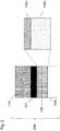
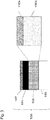
- FIGs. 1 and 2 illustrate a photomask blank according to the present invention, wherein FIG. 1 is a schematic cross-sectional view illustrating a configuration of a photomask blank according to a first embodiment, and FIG. 2 is a schematic cross-sectional view illustrating a configuration of a photomask blank according to a second embodiment.
- a photomask blank 200 illustrated in FIG. 1 is a transmission-type phase shift mask blank, which is a photomask blank used for fabricating a photomask to which exposure light with a wavelength of 193 nm (which is obtained from an exposure light source such as ArF excimer laser) is applied, and includes a light-transmissive substrate 103, a phase shift film 102 formed on the light-transmissive substrate 103 and provides a phase shift effect, and a light shielding film 101 formed on the phase shift film 102 in contact therewith.
- a transmission-type phase shift mask blank which is a photomask blank used for fabricating a photomask to which exposure light with a wavelength of 193 nm (which is obtained from an exposure light source such as ArF excimer laser) is applied, and includes a light-transmissive substrate 103, a phase shift film 102 formed on the light-transmissive substrate 103 and provides a phase shift effect, and a light shielding film 101 formed on the phase shift film 102 in contact
- the light shielding film 101 should preferably include chromium as a main component, which is not etched substantially by fluorine-based dry etching but can be etched by oxygen-containing chlorine-based dry etching, and preferably, the chromium content should be 20 atomic % or more.
- the phase shift film 102 should preferably have a phase difference of 170 through 190 degrees, and a light transmittance of 20 % or more with respect to exposure light, so as to obtain wafer transfer characteristics of a transfer pattern by phase shift effect corresponding to exposure conditions.
- the phase difference of 180 degree is especially preferable to obtain favorable wafer transfer characteristics.
- the phase shift film 102 adopts a two-layer structure composed of a first phase shift film 102b and a second phase shift film 102a.
- a two-layer structure is adopted since a combination of two kinds of films having different refractive index n and extinction coefficient k enables a wider range of film thickness and light transmittance to be realized compared to a single-layer film.
- phase shift film 102 in order to reduce pattern dimension fluctuation by exposure, a transition metal such as molybdenum should not be contained.
- the first phase shift film 102b should be composed of a silicon nitride-based material such as Si 3 N 4
- the second phase shift film 102a should be composed of a silicon oxynitride-based material such as SiON.
- the reason for this composition is that in order to thin the phase shift film while maintaining a phase difference of around 177 degrees, it is necessary to realize a phase shift film including a silicon nitride having a large refractive index n and a relatively small extinction coefficient k.
- a silicon oxynitride-based material having an even smaller extinction coefficient k is laminated as a phase difference adjusting film to realize a two-layer film formed of a film formed of a silicon oxynitride-based material and a film formed of a silicon nitride-based material, which enables to thin the film thickness of the phase shift film 102, and as a result, a good EMF bias as described above can be achieved.
- the reason why a silicon oxynitride-based material such as SiON is used as the second phase shift film 102a is that it has a greater refractive index n than silicon oxide that has been conventionally used as the phase difference adjusting film, and that the film thickness of the phase shift film 102 can be further reduced.
- phase shift film 102 by simultaneously reducing the film thickness of the first phase shift film 102b having a relatively large extinction coefficient k and adjusting the film thickness of the second phase shift film 102a having a relatively small extension coefficient k compared to the first phase shift film 102b, it becomes possible to realize a light transmittance of 30 % or higher while maintaining a phase difference of around 180 degrees.
- the refractive index n and the extinction coefficient k of the first phase shift film 102b and the second phase shift film 102a are known to be varied according to the composition ratio of nitrogen and silicon of the first phase shift film 102b and the composition ratio of oxygen, nitrogen and silicon of the second phase shift film 102a.
- Si 3 N 4 has a large refractive index n and relatively small extinction coefficient k, so that it is suitably used in the first phase shift film 102b.
- SiON has a greater refractive index n and even smaller extinction coefficient k, so that it is suitably used in the second phase shift film 102a.
- Si 3 N 4 is preferably used for the first phase shift film 102b, and SiON is preferably used for the second phase shift film 102a.
- the refractive index n 1 of the first phase shift film 102b may be 2.5 or more and 2.75 or less
- the refractive index n 2 of the second phase shift film 102a may be 1.55 or more and 2.20 or less
- the extinction coefficient k 1 of the first phase shift film 102b may be 0.2 or more and 0.4 or less
- the extinction coefficient k 2 of the second phase shift film 102a may be greater than 0 and no greater than 0.1.
- a film formed on the light-transmissive substrate 103 in contact therewith is referred to as a "lower layer film” and a film formed above the lower layer film is referred to as an "upper layer film”.
- a film formed above the lower layer film is referred to as an "upper layer film”.
- the first phase shift film 102b using silicon nitride-based material such as Si 3 N 4 is formed on the light-transmissive substrate 103 in contact therewith, and the second phase shift film 102a using silicon oxynitride-based material such as SiON is laminated thereon, so that the lower layer film is the first phase shift film 102b using silicon nitride-based material, and the upper layer film is the second phase shift film 102a using silicon oxynitride-based material.
- the lamination order can be opposite.
- the phase shift film 102 may adopt a laminated structure in which the lower layer film is the second phase shift film 102a using silicon oxynitride-based material and the upper layer film is the first phase shift film 102b using silicon nitride-based material.
- the phase shift film 102 adopting a laminated structure in which the lower layer film is the first phase shift film 102b and the upper layer film is the second phase shift film 102a it has better wafer transfer characteristics such as NILS compared to the film adopting an opposite structure (laminated structure in which the upper layer film is the first phase shift film 102b and the lower layer film is the second phase shift film 102a). Specific examples will be described later.
- phase shift film 102 adopting a laminated structure in which the upper layer film is the first phase shift film 102b and the lower layer film is the second phase shift film 102a
- end point detection using plasma emission becomes difficult since the compositions of the light-transmissive substrate 103 and the second phase shift film 102a are extremely similar.
- etching the phase shift film 102 using an electron beam corrector a success rate of correction is deteriorated, since end point detection is difficult by the same reason mentioned above and selectivity with the light-transmissive substrate 103 is small.
- the phase shift film 102 should preferably adopt a laminated structure as illustrated in FIGs.
- phase shift film 102 in which the lower layer film is the first phase shift film 102b and the upper layer film is the second phase shift film 102a will be described.
- the film thickness D 1 of the first phase shift film 102b and the film thickness D 2 of the second phase shift film 102a of the phase shift film 102 should preferably satisfy a relationship of D 1 nm > ⁇ 0.5 ⁇ D 2 nm + 45 ⁇ nm , and D 1 nm ⁇ ⁇ 0.5 ⁇ D 2 nm + 75 ⁇ nm .
- a photomask blank 250 illustrated in FIG. 2 adopts a similar basic configuration as the photomask 200 illustrated in FIG. 1 but differs therefrom in that a resist film 104 is further formed on the light shielding film 101.
- the film thickness of the resist film 104 should preferably be 70 nm or more and 150 nm or less in order to prevent collapse of resist pattern when forming a fine pattern.
- FIG. 1 A configuration as illustrated in FIG. 1 (or FIG. 2 ) is typical in a phase shift mask blank, but a film other than those described above can be laminated.
- a different film in the following description, this film is referred to as a "pattern processing film" can be laminated on the photomask blank illustrated in FIG. 1 .
- pattern processing film an example of a phase shift mask blank having such configuration will be described.
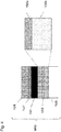
- FIG. 3 is a schematic cross-sectional view of a photomask blank adopting a configuration where a pattern processing film is deposited on the light shielding film 101 of the photomask 200 described with reference to FIG. 1 .
- characteristics (such as the film thickness or the composition) of the light shielding film 101 and the phase shift film 102 are the same as those illustrated in FIGs. 1 and 2 .
- a pattern processing film 107 formed on the light shielding film 101 is a film formed using a material, such as silicon-based material, that can be dry-etched by fluorine-based dry etching.
- a photomask blank 550 illustrated in FIG. 4 is a schematic cross-sectional view illustrating a structure of the photomask blank 550 in which a resist film 108 is further laminated on the pattern processing film 107 of the photomask blank 500 of FIG. 3 .
- the photomask blank 550 is the same as the photomask blank 500 other than the point that the resist film 108 is laminated.
- the film thickness of the resist film 108 can be reduced, and as a result, collapse of resist during the developing step can be reduced.
- the film thickness of the resist film 108 should preferably be 70 nm or more and 100 nm or less to prevent collapse of resist pattern when forming a fine pattern.
- FIG. 5 is a schematic cross-sectional view illustrating a structure of the photomask according to an embodiment of the present invention.
- a photomask 300 illustrated in FIG. 5 is a transmission-type phase shift mask that is fabrication using the photomask 200 (or 250) illustrated in FIG. 1 (or FIG. 2 ) or the photomask blank 500 (or 550) illustrated in FIG. 3 (or FIG. 4 ).
- the photomask 300 illustrated in FIG. 5 is a photomask to which exposure light having a wavelength of 193 nm is applied and includes at least a light-transmissive substrate 103 and a circuit pattern formed by etching the phase shift film 102 on the light-transmissive substrate 103.
- the phase shift film 102 is a film composed by laminating the first phase shift film 102b and the second phase shift film 102a.
- the area denoted by reference number 105 is referred to as an effective area 105, and the effective area 105 is an area including a circuit pattern (area in which the circuit pattern is arranged). Further, a periphery portion pattern 106 composed of the phase shift film 102 and the light shielding film 101 laminated thereon is provided on the periphery portion of the effective area 105.
- the portion of the phase shift film 102 constituting the circuit pattern and the periphery portion pattern is referred to as a "phase shift film pattern 102c".
- light transmittance of the periphery portion pattern 106 with respect to exposure light should preferably be 0.1 % or less.
- the reason of this configuration is to prevent light other than the desired exposure light from being irradiated onto the wafer.
- an exposure device called a stepper is used to transfer the mask pattern onto the resist on the wafer, where exposure region is set by a mechanical shutter and step-and-repeat is performed to realize reduced size projection exposure, and the periphery portion pattern 106 is used to prevent overlap exposure light at the boundary portion of the respective exposure steps. This is because if the transmittance of the periphery portion pattern with respect to exposure wavelength is greater than 0.1 %, the overlap exposure light will create a pattern.
- FIGs. 6 and 7 illustrate a flow of the steps for manufacturing the photomask based on the form of the photomask blank 250 illustrated in FIG. 2 on which the resist film 104 is formed.
- steps ( FIG. 6 ⁇ S-1>, ⁇ S-2> and ⁇ S-3>) for forming an etching mask pattern 101a on the light shielding film 101 by performing dry etching using oxygen-containing chlorine-based gas to the light shielding film 101 using a first resist pattern 104a (obtained by drawing a circuit pattern on the resist film 104 and developing the same) formed on the light shielding film 101 of the photomask blank 250 as a mask are performed.
- phase shift film pattern 102c for forming the phase shift film pattern 102c on the phase shift film 102 by performing dry etching using fluorine-based gas to the phase shift film 102 using an etching mask pattern 101a formed on the light shielding film 101 as a mask is performed.
- a step ( FIG. 6 ⁇ S-5>) for removing the first resist pattern 104a remaining on the etching mask pattern 101a is performed. Thereafter, a step ( FIG. 6 ⁇ S-6>) for applying the resist film 104b thereon and a step ( FIG. 6 ⁇ S-7>) for forming a second resist pattern 104c on the periphery portion by drawing a pattern on the resist film 104b and developing the same are performed. Next, a step ( FIG. 6 ⁇ S-8>) for removing a portion of the light shielding film 101 (etching mask pattern 101a) by performing dry etching using oxygen-containing chlorine-based gas and using the second resist pattern 104c formed on the periphery portion as a mask is performed.
- a step ( FIG. 7 ⁇ S-9>) for forming a periphery portion pattern (composed of the phase shift film pattern 102c and the light shielding film 101 (etching mask pattern 101a) laminated on the phase shift film pattern 102c) by removing the second resist pattern 104c formed on the periphery portion is performed, to thereby fabricate a photomask 400.
- the resist pattern can be removed by sulfuric acid hydration cleaning. Further, a laser drawing device can be used for drawing patterns.
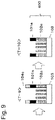
- FIGs. 8 and 9 illustrate a flow of the steps for manufacturing a photomask from the photomask blank 550 illustrated in FIG. 4 .
- steps ( FIG. 8 ⁇ T1 >, ⁇ T2> and ⁇ T3>) for forming a pattern-processing pattern 107a on the pattern processing film 107 by performing dry etching using fluorine-based gas to the pattern processing film 107 using a first resist pattern 108a (obtained by drawing a circuit pattern on the resist film 108 and developing the same) formed on the pattern processing film 107 of the photomask blank 550 as a mask are performed.
- a step ( Fig. 8 ⁇ T-4>) for forming the etching mask pattern 101a on the light shielding film 101 by performing dry etching using oxygen-containing chlorine-based gas to the light shielding film 101 is performed.
- a step ( FIG. 8 ⁇ T-5>) for removing the first resist pattern 108a remaining on the etching mask pattern 101a is performed.
- a step ( FIG. 8 ⁇ T-6>) for forming the phase shift film pattern 102c on the phase shift film 102 by performing dry etching using fluorine-based gas to the phase shift film 102 using the etching mask pattern 101a formed on the light shielding film 101 as a mask is performed.
- the pattern-processing pattern 107a is simultaneously etched with the phase shift film 102 by the fluorine-based gas and removed.
- FIG. 8 ⁇ T-7> a step for applying the resist film 104b is performed, and then a step ( FIG. 8 ⁇ T-8>) for forming the second resist pattern 104c on the periphery portion by drawing a pattern on the resist film 104b and developing the same is performed.
- a step FIG. 8 ⁇ T-8>
- FIG. 9 ⁇ T-9> for removing a portion of the light shielding film 101 (the etching mask pattern 101a) by performing dry etching using oxygen-containing chlorine-based gas and using the second resist pattern 104c formed on the periphery portion as a mask is performed.
- a step ( FIG. 9 ⁇ T-10>) for forming a periphery portion pattern (composed of the phase shift film pattern 102c and the light shielding film 101 (etching mask pattern 101a) laminated on the phase shift film pattern 102c) by removing the second resist pattern 104c formed on the periphery portion is performed, to thereby fabricate the photomask 400.
- the resist pattern can be removed by sulfuric acid hydration cleaning. Further, a laser drawing device can be used for drawing patterns.
- the pattern processing film should preferably be composed of a silicon-based material capable of being etched by fluorine-based gas. Further, the film thickness of the pattern processing film should preferably be 5 nm or more and 10 nm or less to completely etch the pattern-processing pattern 107a during the etching time of the phase shift film 102 in the step illustrated in FIG. 9 ⁇ T-6>.
- wafer transfer characteristics were evaluated by wafer transfer simulation so as to verify the validity of the photomask blank according to the present invention and the photomask manufacturing method using the same.
- phase shift film that is, phase shift film composed of silicon, molybdenum, oxygen and nitrogen.
- the characteristics of the phase shift film according to the comparative example are as follows.
- the composition is as follows: 10 atomic % molybdenum content, 30 atomic % silicon content, 10 atomic % oxygen content, and 50 atomic % nitrogen content.
- the relationship between light transmittance and film thicknesses of the first phase shift film 102b using silicon nitride-based material and the second phase shift film 102a using silicon oxynitride-based material was evaluated.
- the combination of the first phase shift film 102b and the second phase shift film 102a capable of realizing a transmittance of 30 %, 40 %, 50 % and 60 % of the phase shift film 102 is obtained by calculation, which is compared with the comparative example described above.
- phase shift film 102 having a transmittance of 30 %, 40 %, 50 % or 60 % the first phase shift film 102b serving as the lower layer film and the second phase shift film 102a serving as the upper layer film are respectively referred to as "phase shift film 102 of example 1", “phase shift film 102 of example 2", “phase shift film 102 of example 3” and “phase shift film 102 of example 4".
- the film thickness of the first phase shift film 102b and the second phase shift film 102a constituting the phase shift film 102 of examples 1 through 4 in a state where the phase difference at a wavelength of exposure light of ArF excimer laser is approximately 177 degrees, the film thickness of the first phase shift film 102b and the film thickness of the second phase shift film 102a that realize a minimum total film thickness for the respective light transmittances of the phase shift film 102 were computed.
- the computed results film thicknesses of the first phase shift film 102b and the second phase shift film 102a constituting the phase shift film 102 of examples 1 through 4 are shown in the following Table 2.
- the film thickness of the first phase shift film 102b is reduced and the film thickness of the second phase shift film 102a is increased.
- the total film thickness of the phase shift film 102 increases as the light transmittance of the phase shift film 102 increases, but according to the phase shift film 102 of the present embodiment, the total film thickness of the phase shift film 102 (phase shift film 102 of example 1) of the case where the light transmittance is 30 % is 71 nm, which means that a high light transmittance could be realized by a film thickness that is thinner than the phase shift film of the comparative example.
- phase shift film 102 in which the first phase shift film 102b and the second phase shift film 102a are laminated in an opposite order as the phase shift film 102 of examples 1 through 4 was evaluated.
- the phase shift film 102 having a transmittance of 30 %, 40 %, 50 % or 60 % and wherein the first phase shift film 102b is used as the upper layer film and the second phase shift film 102a is used as the lower layer film are respectively referred to as "the phase shift film 102 of example 5", “the phase shift film 102 of example 6",”the phase shift film 102 of example 7", and "the phase shift film 102 of example 8".
- the film thickness of the first phase shift film 102b and the film thickness of the second phase shift film 102a realizing a minimum total film thickness at the respective light transmittances of the phase shift film 102 in a state where the phase difference at the wavelength of exposure light of ArF excimer laser is approximately 177 degrees were computed.
- the results are shown in the following Table 3.
- phase shift film 102 of examples 5 through 8 the film thickness of the first phase shift film 102b was reduced and the film thickness of the second phase shift film 102a was increased as the light transmittance of the phase shift film 102 was increased, similar to the phase shift film 102 of examples 1 through 4. Further, since the total film thickness of the phase shift film 102 according to example 5 (where the light transmittance is 30 %) was 73 nm, it can be recognized that the phase shift film 102 according to the embodiment of the present invention realizes a high light transmittance by a similar film thickness as the phase shift film of the comparative example.
- the change of film thickness of the phase shift film in a state where the light transmittance is varied from 30 % to 100 % was calculated.
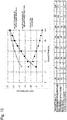
- the results are illustrated in FIG. 10 .
- the table illustrated on the lower portion of FIG. 10 illustrates the film thickness of the second phase shift film, the film thickness of the first phase shift film and the total film thickness of the phase shift film (which is the sum of film thickness of the first phase shift film and film thickness of the second phase shift film) of cases where the light transmittance is 30 %, 40 %, 50 %, 60 %, 70 %, 80 %, 90 % and 100 %, and the graph on the upper part of FIG. 10 shows the result thereof.
- the result of FIG. 10 is a result of calculation of the case where the first phase shift film 102b is used as the lower layer film and the second phase shift film 102a is used as the upper layer film, similar to the phase shift film 102 of examples 1 through 4.
- the total film thickness should be set to a value that is greater 70 nm and is 114 nm or less to realize a light transmittance of 30 % or more.
- Table 4 shows NILS, DOF, MEEF and EMF bias obtained by calculation regarding the photomask 400 using the phase shift films 102 of examples 1 through 4 and the photomask 400 using the phase shift film 102 of the comparative example, improvement rate of the respective examples with respect to the comparative example, and average improvement rate of each example. Evaluation was performed by setting the phase difference of the photomask 400 to 180 degrees, in order to realize more preferable transfer characteristics.
- the photomask according to the present invention is effective in realizing high wafer transfer characteristics.
- the photomask 400 using the phase shift film 102 of example 1 shows the most preferable result.
- the NILS, DOF, MEEF and EMF bias for photomask 400 fabricated using the phase shift film 102 of examples 5 through 8 were evaluated. This evaluation is also performed with the phase difference of the photomask 400 set to 180 degrees.
- the NILS, DOF, MEEF and EMF bias with respect to the light transmittance at the wavelength of exposure light of ArF excimer laser were obtained by calculation, and results of improvement rates of the respective examples with respect to the comparative example and average improvement rate of the respective examples are shown in Table 5.
- the photomasks using the phase shift film 102 of examples 5 through 8 have smaller improvement rates compared to examples 1 through 4. Therefore, the structure where the first phase shift film 102b is used as the lower layer film and the second phase shift film 102a is used as the upper layer film as according to examples 1 through 4 was more preferable since a more favorable wafer transfer characteristics could be obtained.
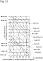
- FIG. 11 illustrates the values of NILS of the phase shift film 102 in which the first phase shift film 102b is used as the lower layer film and the second phase shift film 102a is used as the upper layer film in a state where D 1 is varied within the range of 5 nm to 65 nm and D 2 is varied within the range of 20 nm to 80 nm using wafer transfer simulation, and FIG. 12 shows this result on a graph. Meanwhile, FIG.
- FIG. 13 illustrates the values of NILS of the phase shift film 102 in which the second phase shift film 102a is used as the lower layer film and the first phase shift film 102b is used as the upper layer film in a state where the film thicknesses D 1 and D 2 are varied, and FIG. 14 shows this result in a graph.
- the simulation evaluation was obtained by performing calculation using S-Litho manufactured by Synopsys, Inc., similar to the aforementioned example, and the evaluation conditions were the same as the aforementioned example.
- the NILS of the phase shift film according to the comparative example is 1.79.
- the relationship between the film thickness D 1 of the first phase shift film 102b and the film thickness D 2 of the second phase shift film 102a in which the NILS is improved than the comparative example should preferably fall within an area satisfying the following expressions: D 1 nm > ⁇ 0.5 ⁇ D 2 nm + 45 ⁇ nm , and D 1 nm ⁇ ⁇ 0.5 ⁇ D 2 nm + 75 ⁇ nm .
- D 1 and D 2 should fall within the range satisfying the above expressions.
- the phase shift film according to examples 1 to 8 can be fabricated by making a deposition of the first phase shift film 102b on an optically-polished, six-inch-square synthetic quartz substrate having transmittance with a 0.25 in. film thickness, with using silicon as the target and with using nitrogen and argon as the sputtering gas, and making a deposition of the second phase shift film 102a with using silicon as the target and with using nitrogen, oxygen and argon as the sputtering gas, by a DC magnetron sputtering device.
- the light shielding film 101 is deposited on the phase shift film 102 by a DC magnetron sputtering device with using chromium as the target and with using nitrogen and oxygen as the sputtering gas. Thereby, a mask blank is fabricated. Further, a step for forming a pattern processing film on the light shielding film 101 for fabricating a mask blank as explained in FIG. 3 and the like can be added.
- the photomask blank 200 illustrated in FIG. 1 according to the first embodiment of the present invention was prepared.
- the phase shift film 102 and the light shielding film 101 were set as follows.
- the phase shift film 102 had a total film thickness of 70 nm and a transmittance of 30 % and adopted a two-layer structure including the first phase shift film 102b with a film thickness of 48 nm and the second phase shift film 102a with a film thickness of 22 nm.
- the first phase shift film 102b is formed of silicon nitride
- the second phase shift film 102a is formed of silicon oxynitride.
- the light shielding film 101 was a single-layer film having a film thickness of 70 nm, a chromium content of 50 atomic %, a carbon content of 20 % and a nitrogen content of 30 atomic %, wherein the combination of the phase shift film 102 and the light shielding film 101 realized the transmittance of a wavelength of 193 nm is 0.1 % or smaller.
- a negative-type chemical amplification electron beam resist SEBN 2014 (manufactured by Shin-Etsu Chemical Co., Ltd.) was spin-coated to a film thickness of 150 nm on the photomask 200 to form the resist film 104, and the photomask blank 250 illustrated in FIG. 2 according to the second embodiment was realized ( FIG. 6 ⁇ S-1>).
- ICP Inductively Coupled Plasma
- Gas Cl 2 + O 2 + He
- Gas Pressure 6 mTorr
- ICP power 400 W
- Bias power 15 W
- ICP Inductively Coupled Plasma
- Gas Cl 2 + O 2 + He
- Gas Pressure 6 mTorr
- ICP power 400 W
- Bias power 30 W
- ICP Gas SF 6 + O 2
- Gas Pressure 5 mTorr
- ICP power 325 W
- the first resist pattern 104a was removed by sulfuric acid hydration cleaning ( FIG. 6 ⁇ S-5>).
- the resist film 104b was coated ( FIG. 6 ⁇ S-6>) and drawing was performed by a laser drawing device. Thereafter, development was performed to form the second resist pattern 104c ( FIG. 6 ⁇ S-7>).
- oxygen-containing chlorine-based gas was used to perform dry etching of the etching mask pattern 101a ( FIG. 6 ⁇ S-8>).
- ICP Inductively Coupled Plasma
- Gas Cl 2 + O 2 + He
- Gas Pressure 8 mTorr
- ICP power 500 W
- Bias power 10 W
- the second resist pattern 104c was removed by sulfuric acid hydration cleaning, and the photomask 400 using the photomask blank according to the present invention was fabricated ( FIG. 7 ⁇ S-9>).
- the photomask blank according to the present invention and the photomask manufacturing method using the same can be applied as a phase shift mask blank for fabricating a phase shift mask, and a method for manufacturing the phase shift mask, that has favorable wafer transfer characteristics (NILS, DOF, MEEF and EMF bias), irradiation resistance and pattern collapse resistance during cleaning in a latest photomask for a 14-nm or finer generation of logic devices or 20-nm or finer generation of memory devices.
- wafer transfer characteristics NILS, DOF, MEEF and EMF bias
- 101 Light shielding film
- 101a etching mask pattern
- 102 phase shift film
- 102a second phase shift film
- 102b first phase shift film
- 102c phase shift film pattern
- 103 light-transmissive substrate
- 104 resist film
- 104a first resist pattern
- 104b resist film
- 104c second resist pattern
- 105 effective area
- 106 periphery portion pattern
- 107 pattern processing film
- 107a pattern processing pattern
- 108 resist film
- 300 photomask
- 400 photomask
Landscapes
- Physics & Mathematics (AREA)
- General Physics & Mathematics (AREA)
- Health & Medical Sciences (AREA)
- Engineering & Computer Science (AREA)
- Environmental & Geological Engineering (AREA)
- Epidemiology (AREA)
- Public Health (AREA)
- Preparing Plates And Mask In Photomechanical Process (AREA)
- Exposure And Positioning Against Photoresist Photosensitive Materials (AREA)
Abstract
Description
- The present invention relates to a photomask blank, a photomask and a photomask manufacturing method used for fabricating semiconductor devices and so on.
- As a technique for forming a fine pattern image on a resist material, a photomask manufacturing device and manufacturing method is known where an original pattern is drawn on a photomask blank coated with a photoresist, which is subjected to heat treatment after exposure and developed thereafter to fabricate a resist pattern. Then, a light shielding film and a phase shift film are etched using the resist pattern as a mask. The light shielding film is, for example, a film formed by adding oxygen, nitrogen or carbon to a chromium film, and the phase shift film is, for example, a film formed by adding a transition metal such as molybdenum to silicon, nitrogen or oxygen.
- Recently, along with the high integration of LSI, an exposure light source used for manufacturing semiconductor devices uses shorter wavelength of light from KrF excimer laser (wavelength of 248 nm) to ArF excimer laser (wavelength of 193 nm).
- Based on a relational expression E = hc/λ between light energy E and wavelength λ (wherein h represents Planck's constant and c represents velocity of light), shortening of wavelength of light source means increase of energy per one photon. From the viewpoint of state of energy, it means that the photomask is exposed to a state where chemical reaction is more likely to occur, and therefore, a phenomenon has occurred that has not been an issue in the step of manufacturing a wafer using an exposure wavelength of 248 nm.
- Especially, one of the problems is the variation of mask pattern dimension during exposure. Along with the increase in accumulated amount of exposure irradiated to a line-based pattern on the mask, oxidation of the mask pattern has caused the dimension of the line-based pattern to be enlarged, and the impact that the variation of dimension provides on the manufacturing processes of leading-edge wafers has become significant.
- Further, in a process of manufacturing leading-edge wafers, in order to improve wafer transfer characteristics, a mainstream phase shift mask has a phase difference between an ArF excimer laser beam transmitted through a light-transmissive substrate and an ArF excimer laser beam transmitted through both the light-transmissive substrate and the phase shift film (hereinafter simply referred to as "phase difference") of between 170 through 190 degrees and a light transmittance of 6 %. If the light transmittance of the phase shift film on the phase shift mask is 6 %, a most favorable wafer transfer characteristics is achieved where the phase difference is around 180 degrees.
- In a state of forming a phase shift film dry-etched using a fluorine-based gas where the film thickness of the phase shift film is set to have a phase difference of around 177 degrees, a method of processing the light-transmissive substrate for about 3 nm simultaneously to realize a final phase difference of around 180 degrees is known.
- Normalized Image Log Slope (NILS) that represents a slope of contrast of optical energy distribution that passes through the photomask to form a pattern image on the wafer resist, Depth of Focus (DOF) that represents a distance from a focus capable of forming the pattern stably, Mask Error Enhancement Factor (MEEF) that represents a degree of error of dimension on the mask being amplified on the wafer dimension, and a bias (Electro Magnetic Field Bias: EMF bias) related to an electromagnetic field effect in the mask pattern, are used as items for expressing wafer transfer characteristics.
- In 14-nm or finer generation of logic devices or in 20-nm or finer generation of memory devices, transmittance of 6 % is not sufficient, so a high-transmittance phase shift mask is gathering attention.
- By increasing the light transmittance, the phase shift effect is further enhanced, and favorable wafer transfer characteristics can be achieved.
- In 14-nm or finer generation of logic devices or in 20-nm or finer generation of memory devices, the dimension of the pattern on the wafer is required to be even finer, and a high transmittance phase shift mask having a light transmittance of 20 % or higher is desired to obtain higher wafer transfer characteristics.
- However, the phase shift film thickness must be increased to realize higher light transmittance while maintaining the phase difference of the phase shift film to around 177 degrees.
- Further, along with the refinement of the photomask, a fine assist pattern is required, but a problem occurs in a cleaning step for removing foreign substances in which the assist pattern is collapsed and lost by the impact caused by cleaning fluid or rinse fluid. This problem is caused by the increased thickness of the phase shift film, and in order to improve durability against cleaning, the film thickness of the phase shift film must be reduced.
- At the same time, a phase shift film that is as thin as possible is preferred, since the thinner the film thickness of the phase shift film is, the better the EMF bias is.
- A silicon nitride film having eliminated transition metal such as molybdenum from the phase shift film is drawing attention, since it has high light transmittance of the phase shift film, so that good wafer transfer characteristics (NILS, DOF, MEEF, EMF bias)can be realized and pattern variation by exposure is reduced.
-
- [JPL1] Japanese Patent Application Laid-Open Publication No.
2010-9038 - [JPL2] Japanese Patent Application Laid-Open Publication No.
2016-191882 - In 14-nm or finer generation of logic devices, double exposure or quadruplex exposure are performed during the wafer manufacturing process, so that there is a need to minimize the variation of mask dimension during wafer exposure. In contrast, in order to improve irradiation resistance, a prior art halftone-type phase shift mask forms a phase shift film mainly using silicon nitride and reducing the content of transition metal such as molybdenum. (JPL1 and JPL2).
- Further, in order to realize favorable wafer transfer characteristics (NILS, DOF, MEEF, EMF bias) during the wafer manufacturing process, the light transmittance of the phase shift film is required to be 6 % or higher. (JPL1 and JPL2)
- Further, along with the refinement of the photomask, a fine assist pattern is required, so that a phase shift film having a small film thickness is preferable to reduce the influence of the cleaning fluid on the pattern during the cleaning step of the photomask. (JPL1 and JPL2)
- However, according the method disclosed in JPL1 or JPL 2, the light transmittance of the phase shift film is respectively 9 % or more and 30 % or less (JPL1) or 3 % or more and 12 % or less (JPL2), and it is difficult to correspond to high transmittance that is required in leading-edge photomasks.
- In order to increase the light transmittance by adding nitrogen or oxygen gas, it is necessary to increase the film thickness of the phase shift film to maintain a phase difference of around 177 degrees, and the possibility of collapsing of the pattern during cleaning is increased.
- Further, silicon nitride is effective in increasing the light transmittance while suppressing the film thickness of the phase shift film to a minimum and maintaining a phase difference around 177 degrees, but in a monolayer film of silicon nitride, the light transmittance cannot be increased higher than 18 %.
- The present invention aims at solving the problems described above, and the object thereof is to provide a photomask blank, a photomask and a photomask manufacturing method that adopts a phase shift film as thin as possible, that has favorable wafer transfer characteristics (NILS, DOF, MEEF and EMF bias) and enables to ensure both irradiation resistance and pattern collapse resistance during cleaning.
- A photomask blank according to one aspect of the present invention relates to a photomask blank used for fabricating a photomask to which an exposure light with a wavelength of 193 nm is applied, the photomask blank including a light-transmissive substrate, a phase shift film formed on the light-transmissive substrate and providing a phase shift effect, and a light shielding film formed on the phase shift film. The phase shift film is composed by laminating a first phase shift film using a silicon nitride-based material, and a second phase shift film using a silicon oxynitride-based material. Further, the phase shift film has a light transmittance of 30 % or more with respect to the exposure light, the first phase shift film has a refractive index n1 of 2.5 or more and 2.75 or less, the second phase shift film has a refractive index n2 of 1.55 or more and 2.20 or less, the first phase shift film has an extinction coefficient k1 of 0.2 or more and 0.4 or less, and the second phase shift film has an extinction coefficient k2 that is greater than 0 and no greater than 0.1.
- According further to the photomask blank, a film thickness D1 of the first phase shift film and a film thickness D2 of the second phase shift film should preferably satisfy the following relationship:


- Further according to the photomask blank, the light shielding film should preferably not be etched by fluorine-based dry etching and be etched by oxygen-containing chlorine-based dry etching and should preferably have a chromium content of 20 atomic % or more.
- A photomask according to one aspect of the present invention relates to a photomask to which an exposure light with a wavelength of 193 nm is applied, the photomask including a light-transmissive substrate, and a circuit pattern which is a pattern formed on a phase shift film laminated on the light-transmissive substrate. The phase shift film is composed by laminating a first phase shift film using a silicon nitride-based material, and a second phase shift film using a silicon oxynitride-based material. Further, the phase shift film has a light transmittance of 30 % or more with respect to the exposure light, the first phase shift film has a refractive index n1 of 2.5 or more and 2.75 or less, the second phase shift film has a refractive index n2 of 1.55 or more and 2.20 or less, the first phase shift film has an extinction coefficient k1 of 0.2 or more and 0.4 or less, and the second phase shift film has an extinction coefficient k2 that is greater than 0 and no greater than 0.1.
- According to this photomask, a film thickness D1 of the first phase shift film and a film thickness D2 of the second phase shift film should preferably satisfy the following relationship:


- According to this photomask, a light shielding film should preferably be laminated on the phase shift film positioned at a periphery portion of an effective area including the circuit pattern, and the light shielding film should preferably be mainly composed of chromium that may not substantially be etched by fluorine-based dry etching but can be etched by oxygen-containing chlorine-based dry etching.
- Further, a photomask manufacturing method according to one aspect of the present invention relates to a photomask manufacturing method using the above-described photomask blank, the method including a step of forming a pattern on the light shielding film by performing dry etching using an oxygen-containing chlorine-based gas to the light shielding film, a step of forming a circuit pattern and a periphery portion pattern that forms a periphery portion of an area including the circuit pattern on the phase shift film by performing dry etching using a fluorine-based gas to the phase shift film using the pattern formed on the light shielding film as a mask, a step of forming a resist pattern on the periphery portion pattern, and performing dry etching using an oxygen-containing chlorine-based gas using the resist pattern as a mask to remove a portion of the light shielding film, and a step of removing the resist pattern.
- According to the present invention, it becomes possible to realize a photomask blank or a photomask having a good irradiation resistance while ensuring wafer transfer characteristics.
-
- [
FIG. 1] FIG. 1 is a schematic cross-sectional view illustrating a configuration of a photomask blank according to a first embodiment. - [
FIG. 2] FIG. 2 is a schematic cross-sectional view illustrating a configuration of a photomask blank according to a second embodiment. - [
FIG. 3] FIG. 3 is a schematic cross-sectional view illustrating a configuration of a photomask blank in which a pattern processing film is deposited on a light shielding film. - [
FIG. 4] FIG. 4 is a schematic cross-sectional view illustrating a configuration of a photomask blank in which a pattern processing film and a resist film are laminated on the light shielding film. - [
FIG. 5] FIG. 5 is a schematic cross-sectional view illustrating a configuration of a photomask according to the embodiment of the present invention. - [
FIG. 6] FIG. 6 is a schematic view illustrating a photomask manufacturing method according to the embodiment of the present invention. - [
FIG. 7] FIG. 7 is a schematic view illustrating a photomask manufacturing method according to the embodiment of the present invention. - [
FIG. 8] FIG. 8 is a schematic view of a photomask manufacturing method using a photomask blank in which a pattern processing film is deposited on a light shielding film. - [
FIG. 9] FIG. 9 is a schematic view of a photomask manufacturing method according to the embodiment of the present invention in which the pattern processing film is deposited on the light shielding film. - [
FIG. 10] FIG. 10 is a view illustrating a relationship between film thickness and light transmittance of the phase shift film. - [
FIG. 11] FIG. 11 is a view illustrating a relationship between film thickness D1 of a first phase shift film and a second phase shift film D2, and NILS. - [
FIG. 12] FIG. 12 is a graph illustrating a relationship between film thickness D1 of the first phase shift film and film thickness D2 of the second phase shift film, and NILS. - [
FIG. 13] FIG. 13 is a view illustrating a relationship between film thickness D1 of the first phase shift film and film thickness D2 of the second phase shift film, and NILS. - [
FIG. 14] FIG. 14 is a graph illustrating a relationship between film thickness D1 of the first phase shift film and film thickness D2 of the second phase shift film, and NILS. - Now, an embodiment of the present invention will be described with reference to the drawings. In the respective drawings, the same components are assigned with the same reference numbers, and descriptions thereof may be omitted. The drawings referred to in the description may show characteristic portions in enlarged views to help understand the characteristics, and dimensions of the respective components do not necessarily correspond to the actual dimensions.
-
FIGs. 1 and2 illustrate a photomask blank according to the present invention, whereinFIG. 1 is a schematic cross-sectional view illustrating a configuration of a photomask blank according to a first embodiment, andFIG. 2 is a schematic cross-sectional view illustrating a configuration of a photomask blank according to a second embodiment. - A
photomask blank 200 illustrated inFIG. 1 is a transmission-type phase shift mask blank, which is a photomask blank used for fabricating a photomask to which exposure light with a wavelength of 193 nm (which is obtained from an exposure light source such as ArF excimer laser) is applied, and includes a light-transmissive substrate 103, aphase shift film 102 formed on the light-transmissive substrate 103 and provides a phase shift effect, and alight shielding film 101 formed on thephase shift film 102 in contact therewith. - The
light shielding film 101 should preferably include chromium as a main component, which is not etched substantially by fluorine-based dry etching but can be etched by oxygen-containing chlorine-based dry etching, and preferably, the chromium content should be 20 atomic % or more. - The
phase shift film 102 should preferably have a phase difference of 170 through 190 degrees, and a light transmittance of 20 % or more with respect to exposure light, so as to obtain wafer transfer characteristics of a transfer pattern by phase shift effect corresponding to exposure conditions. The phase difference of 180 degree is especially preferable to obtain favorable wafer transfer characteristics. - The
phase shift film 102 adopts a two-layer structure composed of a firstphase shift film 102b and a secondphase shift film 102a. A two-layer structure is adopted since a combination of two kinds of films having different refractive index n and extinction coefficient k enables a wider range of film thickness and light transmittance to be realized compared to a single-layer film. - Regarding the
phase shift film 102, in order to reduce pattern dimension fluctuation by exposure, a transition metal such as molybdenum should not be contained. Further, the firstphase shift film 102b should be composed of a silicon nitride-based material such as Si3N4, and the secondphase shift film 102a should be composed of a silicon oxynitride-based material such as SiON. The reason for this composition is that in order to thin the phase shift film while maintaining a phase difference of around 177 degrees, it is necessary to realize a phase shift film including a silicon nitride having a large refractive index n and a relatively small extinction coefficient k. However, in the case of a single-layer film using silicon nitride, the light transmittance is approximately 18 % at most, and a higher light transmittance cannot be realized. Therefore, a silicon oxynitride-based material having an even smaller extinction coefficient k is laminated as a phase difference adjusting film to realize a two-layer film formed of a film formed of a silicon oxynitride-based material and a film formed of a silicon nitride-based material, which enables to thin the film thickness of thephase shift film 102, and as a result, a good EMF bias as described above can be achieved. - Further, the reason why a silicon oxynitride-based material such as SiON is used as the second
phase shift film 102a is that it has a greater refractive index n than silicon oxide that has been conventionally used as the phase difference adjusting film, and that the film thickness of thephase shift film 102 can be further reduced. - Regarding the
phase shift film 102, by simultaneously reducing the film thickness of the firstphase shift film 102b having a relatively large extinction coefficient k and adjusting the film thickness of the secondphase shift film 102a having a relatively small extension coefficient k compared to the firstphase shift film 102b, it becomes possible to realize a light transmittance of 30 % or higher while maintaining a phase difference of around 180 degrees. - The refractive index n and the extinction coefficient k of the first
phase shift film 102b and the secondphase shift film 102a are known to be varied according to the composition ratio of nitrogen and silicon of the firstphase shift film 102b and the composition ratio of oxygen, nitrogen and silicon of the secondphase shift film 102a. Among silicon nitrides existing stably in nature, Si3N4 has a large refractive index n and relatively small extinction coefficient k, so that it is suitably used in the firstphase shift film 102b. Further, among silicon nitride oxides existing stably in nature, SiON has a greater refractive index n and even smaller extinction coefficient k, so that it is suitably used in the secondphase shift film 102a. Therefore, Si3N4 is preferably used for the firstphase shift film 102b, and SiON is preferably used for the secondphase shift film 102a. If Si3N4 is used for the firstphase shift film 102b and SiON is used for the secondphase shift film 102a, the refractive index n1 of the firstphase shift film 102b may be 2.5 or more and 2.75 or less, the refractive index n2 of the secondphase shift film 102a may be 1.55 or more and 2.20 or less, the extinction coefficient k1 of the firstphase shift film 102b may be 0.2 or more and 0.4 or less, and the extinction coefficient k2 of the secondphase shift film 102a may be greater than 0 and no greater than 0.1. - In the following description, a film formed on the light-
transmissive substrate 103 in contact therewith is referred to as a "lower layer film" and a film formed above the lower layer film is referred to as an "upper layer film". In thephase shift film 102 illustrated inFIGs. 1 or2 , the firstphase shift film 102b using silicon nitride-based material such as Si3N4 is formed on the light-transmissive substrate 103 in contact therewith, and the secondphase shift film 102a using silicon oxynitride-based material such as SiON is laminated thereon, so that the lower layer film is the firstphase shift film 102b using silicon nitride-based material, and the upper layer film is the secondphase shift film 102a using silicon oxynitride-based material. However, the lamination order can be opposite. That is, thephase shift film 102 may adopt a laminated structure in which the lower layer film is the secondphase shift film 102a using silicon oxynitride-based material and the upper layer film is the firstphase shift film 102b using silicon nitride-based material. Incidentally, as illustrated inFIGs. 1 and2 , in the case of thephase shift film 102 adopting a laminated structure in which the lower layer film is the firstphase shift film 102b and the upper layer film is the secondphase shift film 102a, it has better wafer transfer characteristics such as NILS compared to the film adopting an opposite structure (laminated structure in which the upper layer film is the firstphase shift film 102b and the lower layer film is the secondphase shift film 102a). Specific examples will be described later. - Further, in the case of the
phase shift film 102 adopting a laminated structure in which the upper layer film is the firstphase shift film 102b and the lower layer film is the secondphase shift film 102a, while dry-etching thephase shift film 102 using fluorine-based gas, end point detection using plasma emission becomes difficult since the compositions of the light-transmissive substrate 103 and the secondphase shift film 102a are extremely similar. Further, in etching thephase shift film 102 using an electron beam corrector, a success rate of correction is deteriorated, since end point detection is difficult by the same reason mentioned above and selectivity with the light-transmissive substrate 103 is small. In consideration of these issues, thephase shift film 102 should preferably adopt a laminated structure as illustrated inFIGs. 1 and2 , where the lower layer film is the firstphase shift film 102b and the upper layer film is the secondphase shift film 102a. Therefore, in the following description, unless denoted otherwise, thephase shift film 102 in which the lower layer film is the firstphase shift film 102b and the upper layer film is the secondphase shift film 102a will be described. - Further, considering the wafer transfer characteristics such as NILS, the film thickness D1 of the first
phase shift film 102b and the film thickness D2 of the secondphase shift film 102a of thephase shift film 102 should preferably satisfy a relationship of

- A
photomask blank 250 illustrated inFIG. 2 adopts a similar basic configuration as thephotomask 200 illustrated inFIG. 1 but differs therefrom in that a resistfilm 104 is further formed on thelight shielding film 101. - The film thickness of the resist
film 104 should preferably be 70 nm or more and 150 nm or less in order to prevent collapse of resist pattern when forming a fine pattern. - A configuration as illustrated in
FIG. 1 (orFIG. 2 ) is typical in a phase shift mask blank, but a film other than those described above can be laminated. For example, a different film (in the following description, this film is referred to as a "pattern processing film") can be laminated on the photomask blank illustrated inFIG. 1 . Hereafter, an example of a phase shift mask blank having such configuration will be described. -
FIG. 3 is a schematic cross-sectional view of a photomask blank adopting a configuration where a pattern processing film is deposited on thelight shielding film 101 of thephotomask 200 described with reference toFIG. 1 . In aphotomask blank 500 ofFIG. 3 , characteristics (such as the film thickness or the composition) of thelight shielding film 101 and thephase shift film 102 are the same as those illustrated inFIGs. 1 and2 . Apattern processing film 107 formed on thelight shielding film 101 is a film formed using a material, such as silicon-based material, that can be dry-etched by fluorine-based dry etching. - Meanwhile, a photomask blank 550 illustrated in
FIG. 4 is a schematic cross-sectional view illustrating a structure of the photomask blank 550 in which a resistfilm 108 is further laminated on thepattern processing film 107 of thephotomask blank 500 ofFIG. 3 . Thephotomask blank 550 is the same as thephotomask blank 500 other than the point that the resistfilm 108 is laminated. - By forming the photomask blank to have a configuration as illustrated in
FIGs. 3 and4 , the film thickness of the resistfilm 108 can be reduced, and as a result, collapse of resist during the developing step can be reduced. The film thickness of the resistfilm 108 should preferably be 70 nm or more and 100 nm or less to prevent collapse of resist pattern when forming a fine pattern. -
FIG. 5 is a schematic cross-sectional view illustrating a structure of the photomask according to an embodiment of the present invention. Aphotomask 300 illustrated inFIG. 5 is a transmission-type phase shift mask that is fabrication using the photomask 200 (or 250) illustrated inFIG. 1 (orFIG. 2 ) or the photomask blank 500 (or 550) illustrated inFIG. 3 (orFIG. 4 ). Thephotomask 300 illustrated inFIG. 5 is a photomask to which exposure light having a wavelength of 193 nm is applied and includes at least a light-transmissive substrate 103 and a circuit pattern formed by etching thephase shift film 102 on the light-transmissive substrate 103. As described above, thephase shift film 102 is a film composed by laminating the firstphase shift film 102b and the secondphase shift film 102a. - In
FIG. 5 , the area denoted byreference number 105 is referred to as aneffective area 105, and theeffective area 105 is an area including a circuit pattern (area in which the circuit pattern is arranged). Further, aperiphery portion pattern 106 composed of thephase shift film 102 and thelight shielding film 101 laminated thereon is provided on the periphery portion of theeffective area 105. In the following description, the portion of thephase shift film 102 constituting the circuit pattern and the periphery portion pattern is referred to as a "phaseshift film pattern 102c". - Incidentally, light transmittance of the
periphery portion pattern 106 with respect to exposure light should preferably be 0.1 % or less. The reason of this configuration is to prevent light other than the desired exposure light from being irradiated onto the wafer. Normally, an exposure device called a stepper is used to transfer the mask pattern onto the resist on the wafer, where exposure region is set by a mechanical shutter and step-and-repeat is performed to realize reduced size projection exposure, and theperiphery portion pattern 106 is used to prevent overlap exposure light at the boundary portion of the respective exposure steps. This is because if the transmittance of the periphery portion pattern with respect to exposure wavelength is greater than 0.1 %, the overlap exposure light will create a pattern. - Next, a photomask manufacturing method according to the embodiment of the present invention will be described.
FIGs. 6 and7 illustrate a flow of the steps for manufacturing the photomask based on the form of the photomask blank 250 illustrated inFIG. 2 on which the resistfilm 104 is formed. - At first, steps (
FIG. 6 <S-1>, <S-2> and <S-3>) for forming anetching mask pattern 101a on thelight shielding film 101 by performing dry etching using oxygen-containing chlorine-based gas to thelight shielding film 101 using a first resistpattern 104a (obtained by drawing a circuit pattern on the resistfilm 104 and developing the same) formed on thelight shielding film 101 of the photomask blank 250 as a mask are performed. Next, a step (Fig. 6 <S-4>) for forming the phaseshift film pattern 102c on thephase shift film 102 by performing dry etching using fluorine-based gas to thephase shift film 102 using anetching mask pattern 101a formed on thelight shielding film 101 as a mask is performed. - Next, a step (
FIG. 6 <S-5>) for removing the first resistpattern 104a remaining on theetching mask pattern 101a is performed. Thereafter, a step (FIG. 6 <S-6>) for applying the resistfilm 104b thereon and a step (FIG. 6 <S-7>) for forming a second resistpattern 104c on the periphery portion by drawing a pattern on the resistfilm 104b and developing the same are performed. Next, a step (FIG. 6 <S-8>) for removing a portion of the light shielding film 101 (etching mask pattern 101a) by performing dry etching using oxygen-containing chlorine-based gas and using the second resistpattern 104c formed on the periphery portion as a mask is performed. Lastly, a step (FIG. 7 <S-9>) for forming a periphery portion pattern (composed of the phaseshift film pattern 102c and the light shielding film 101 (etching mask pattern 101a) laminated on the phaseshift film pattern 102c) by removing the second resistpattern 104c formed on the periphery portion is performed, to thereby fabricate aphotomask 400. The resist pattern can be removed by sulfuric acid hydration cleaning. Further, a laser drawing device can be used for drawing patterns. -
FIGs. 8 and9 illustrate a flow of the steps for manufacturing a photomask from the photomask blank 550 illustrated inFIG. 4 . - At first, steps (
FIG. 8 <T1 >, <T2> and <T3>) for forming a pattern-processing pattern 107a on thepattern processing film 107 by performing dry etching using fluorine-based gas to thepattern processing film 107 using a first resistpattern 108a (obtained by drawing a circuit pattern on the resistfilm 108 and developing the same) formed on thepattern processing film 107 of the photomask blank 550 as a mask are performed. Next, a step (Fig. 8 <T-4>) for forming theetching mask pattern 101a on thelight shielding film 101 by performing dry etching using oxygen-containing chlorine-based gas to thelight shielding film 101 is performed. - Next, a step (
FIG. 8 <T-5>) for removing the first resistpattern 108a remaining on theetching mask pattern 101a is performed. - Thereafter, a step (
FIG. 8 <T-6>) for forming the phaseshift film pattern 102c on thephase shift film 102 by performing dry etching using fluorine-based gas to thephase shift film 102 using theetching mask pattern 101a formed on thelight shielding film 101 as a mask is performed. Here, the pattern-processing pattern 107a is simultaneously etched with thephase shift film 102 by the fluorine-based gas and removed. - The steps performed hereafter are similar to the steps (
FIG. 6 <S-6> toFIG. 7 <S-9>) described with reference toFIGs. 6 and7 . At first, as illustrated inFIG. 8 <T-7>, a step for applying the resistfilm 104b is performed, and then a step (FIG. 8 <T-8>) for forming the second resistpattern 104c on the periphery portion by drawing a pattern on the resistfilm 104b and developing the same is performed. Next, a step (FIG. 9 <T-9>) for removing a portion of the light shielding film 101 (theetching mask pattern 101a) by performing dry etching using oxygen-containing chlorine-based gas and using the second resistpattern 104c formed on the periphery portion as a mask is performed. Lastly, a step (FIG. 9 <T-10>) for forming a periphery portion pattern (composed of the phaseshift film pattern 102c and the light shielding film 101 (etching mask pattern 101a) laminated on the phaseshift film pattern 102c) by removing the second resistpattern 104c formed on the periphery portion is performed, to thereby fabricate thephotomask 400. The resist pattern can be removed by sulfuric acid hydration cleaning. Further, a laser drawing device can be used for drawing patterns. - As described above, the pattern processing film should preferably be composed of a silicon-based material capable of being etched by fluorine-based gas. Further, the film thickness of the pattern processing film should preferably be 5 nm or more and 10 nm or less to completely etch the pattern-
processing pattern 107a during the etching time of thephase shift film 102 in the step illustrated inFIG. 9 <T-6>. - In this example, wafer transfer characteristics were evaluated by wafer transfer simulation so as to verify the validity of the photomask blank according to the present invention and the photomask manufacturing method using the same.
- Simulation evaluation was obtained by performing calculation using S-Litho manufactured by Synopsys, Inc.
-
- NA: 1.35
- Sigma: QS X-0 deg, BL: 32 deg/Y - 90 deg, BL: 37 deg
- Polarization: Azimuthally polarization
- Target: 52 nm dense hole (Negative tone develop)
- Pitch: 100 nm
- Refractive index n1 of first
phase shift film 102b: 2.60 - Extinction coefficient k1 of first
phase shift film 102b: 0.35 - Refractive index n2 of second
phase shift film 102a: 1.85 - Extinction coefficient k2 of second
phase shift film 102a: 0.004 - In order to verify the validity of the photomask blank according to the present invention, as a comparative example, wafer transfer simulation was also performed to a conventional phase shift film, that is, phase shift film composed of silicon, molybdenum, oxygen and nitrogen. The characteristics of the phase shift film according to the comparative example are as follows.
- Transmittance: 6 %
Film thickness: 75 nm
Phase difference: 177.0 degrees
Refractive index n: 2.3
Extinction coefficient k: 0.55 - The composition is as follows: 10 atomic % molybdenum content, 30 atomic % silicon content, 10 atomic % oxygen content, and 50 atomic % nitrogen content.
- The result of wafer transfer simulation regarding the phase shift film according to the comparative example is illustrated in Table 1.
[Table 1] COMPARATIVE EXAMPLE LIGHT TRANSMITTANCE OF PHASE SHIFT FILM 102 [%] 6% NILS 1.79 DOF[um] 0.51 MEEF 6.2 EMF BIAS 13.0 - At first, the relationship between light transmittance and film thicknesses of the first
phase shift film 102b using silicon nitride-based material and the secondphase shift film 102a using silicon oxynitride-based material was evaluated. In the present example, the combination of the firstphase shift film 102b and the secondphase shift film 102a capable of realizing a transmittance of 30 %, 40 %, 50 % and 60 % of thephase shift film 102 is obtained by calculation, which is compared with the comparative example described above. In the following description, regarding thephase shift film 102 having a transmittance of 30 %, 40 %, 50 % or 60 %, the firstphase shift film 102b serving as the lower layer film and the secondphase shift film 102a serving as the upper layer film are respectively referred to as "phase shift film 102 of example 1", "phase shift film 102 of example 2", "phase shift film 102 of example 3" and "phase shift film 102 of example 4". - Upon computing the film thicknesses of the first
phase shift film 102b and the secondphase shift film 102a constituting thephase shift film 102 of examples 1 through 4, in a state where the phase difference at a wavelength of exposure light of ArF excimer laser is approximately 177 degrees, the film thickness of the firstphase shift film 102b and the film thickness of the secondphase shift film 102a that realize a minimum total film thickness for the respective light transmittances of thephase shift film 102 were computed. The computed results (film thicknesses of the firstphase shift film 102b and the secondphase shift film 102a constituting thephase shift film 102 of examples 1 through 4) are shown in the following Table 2.[Table 2] COMPARATIVE EXAMPLE EXAMPLE 1 EXAMPLE 2 EXAMPLE 3 EXAMPLE 4 LIGHT TRANSMITTANCE OF PHASE SHIFT FILM 102 [%] 6% 30% 40% 50% 60% FILM THICKNESS OF SECOND PHASE SHIFT FILM 102a [nm]NONE 22 51 62 73 FILM THICKNESS OF FIRST PHASE SHIFT FILM 102b [nm]NONE 49 33 28 22 TOTAL FILM THICKNESS OF PHASE SHIFT FILM 102 [nm] 75 71 84 90 95 PHASE DIFFERENCE [degrees] 177.0 177.0 177.0 177.0 177.0 - As can be recognized from Table 2, as the light transmittance of the
phase shift film 102 increases, the film thickness of the firstphase shift film 102b is reduced and the film thickness of the secondphase shift film 102a is increased. Further, the total film thickness of thephase shift film 102 increases as the light transmittance of thephase shift film 102 increases, but according to thephase shift film 102 of the present embodiment, the total film thickness of the phase shift film 102 (phase shift film 102 of example 1) of the case where the light transmittance is 30 % is 71 nm, which means that a high light transmittance could be realized by a film thickness that is thinner than the phase shift film of the comparative example. - Next, the
phase shift film 102 in which the firstphase shift film 102b and the secondphase shift film 102a are laminated in an opposite order as thephase shift film 102 of examples 1 through 4 was evaluated. In the following description, thephase shift film 102 having a transmittance of 30 %, 40 %, 50 % or 60 % and wherein the firstphase shift film 102b is used as the upper layer film and the secondphase shift film 102a is used as the lower layer film are respectively referred to as "thephase shift film 102 of example 5", "thephase shift film 102 of example 6","thephase shift film 102 of example 7", and "thephase shift film 102 of example 8". Similar to thephase shift film 102 of examples 1 through 4, in order to obtain the film thicknesses of the firstphase shift film 102b and the secondphase shift film 102a constituting thephase shift film 102 of examples 5 through 8, the film thickness of the firstphase shift film 102b and the film thickness of the secondphase shift film 102a realizing a minimum total film thickness at the respective light transmittances of thephase shift film 102 in a state where the phase difference at the wavelength of exposure light of ArF excimer laser is approximately 177 degrees were computed. The results are shown in the following Table 3.[Table 3] COMPARATIVE EXAMPLE EXAMPLE 5 EXAMPLE 6 EXAMPLE 7 EXAMPLE 8 LIGHT TRANSMITTANCE OF PHASE SHIFT FILM 102 [%] 6% 30% 40% 50% 60% FILM THICKNESS OF FIRST PHASE SHIFT FILM 102b [nm]NONE 43 33 18 10 FILM THICKNESS OF SECOND PHASE SHIFT FILM 102a [nm]NONE 30 52 80 92 TOTAL FILM THICKNESS OF PHASE SHIFT FILM 102 [nm] 75 73 85 98 102 PHASE DIFFERENCE [degrees] 177.0 177.0 177.0 177.0 177.0 - It has been recognized that also according to the
phase shift film 102 of examples 5 through 8, the film thickness of the firstphase shift film 102b was reduced and the film thickness of the secondphase shift film 102a was increased as the light transmittance of thephase shift film 102 was increased, similar to thephase shift film 102 of examples 1 through 4. Further, since the total film thickness of thephase shift film 102 according to example 5 (where the light transmittance is 30 %) was 73 nm, it can be recognized that thephase shift film 102 according to the embodiment of the present invention realizes a high light transmittance by a similar film thickness as the phase shift film of the comparative example. - Further, the change of film thickness of the phase shift film in a state where the light transmittance is varied from 30 % to 100 % was calculated. The results are illustrated in
FIG. 10 . The table illustrated on the lower portion ofFIG. 10 illustrates the film thickness of the second phase shift film, the film thickness of the first phase shift film and the total film thickness of the phase shift film (which is the sum of film thickness of the first phase shift film and film thickness of the second phase shift film) of cases where the light transmittance is 30 %, 40 %, 50 %, 60 %, 70 %, 80 %, 90 % and 100 %, and the graph on the upper part ofFIG. 10 shows the result thereof. The result ofFIG. 10 is a result of calculation of the case where the firstphase shift film 102b is used as the lower layer film and the secondphase shift film 102a is used as the upper layer film, similar to thephase shift film 102 of examples 1 through 4. - As can be recognized from
FIG. 10 , the total film thickness should be set to a value that is greater 70 nm and is 114 nm or less to realize a light transmittance of 30 % or more. - Further, based on Tables 2 and 3, it can be recognized that the structure where the first
phase shift film 102b is used as the lower layer film and the secondphase shift film 102a is used as the upper layer film (examples 1 through 4) realizes a thinner film thickness than thephase shift film 102 of examples 5 through 8. - Next, Table 4 shows NILS, DOF, MEEF and EMF bias obtained by calculation regarding the
photomask 400 using thephase shift films 102 of examples 1 through 4 and thephotomask 400 using thephase shift film 102 of the comparative example, improvement rate of the respective examples with respect to the comparative example, and average improvement rate of each example. Evaluation was performed by setting the phase difference of thephotomask 400 to 180 degrees, in order to realize more preferable transfer characteristics.[Table 4] COMPARATIVE EXAMPLE EXAMPLE 1 EXAMPLE 2 EXAMPLE 3 EXAMPLE 4 LIGHT TRANSMITTANCE OF PHASE SHIFT FILM 102 [%] 6% 30% 40% 50% 60% NILS 1.79 2.26 1.94 2.01 1.98 DOF[um] 0.51 0.53 0.52 0.53 0.52 MEEF 6.2 5.0 5.8 5.3 5.5 EMF BIAS 13.0 8.4 6.1 6.9 6.1 NILS IMPROVEMENT RATE TO COMPARATIVE EXAMPLE [%] 25.8 8.17 12.08 10.41 DOF IMPROVEMENT RATE TO COMPARATIVE EXAMPLE [%] 3.6 2.6 4.5 2.6 MEEF IMPROVEMENT RATE TO COMPARATIVE EXAMPLE [%] 19.9 6.1 15.3 11.1 EMF BIAS IMPROVEMENT RATE TO COMPARATIVE EXAMPLE [%] 35.3 53.1 47.0 53.2 AVERAGE VALUE OF IMPROVEMENT RATE [%] 21.2 17.5 23.2 22.3 - As a result, it has been recognized that all items were improved in the
photomask 400 using thephase shift film 102 of examples 1 through 4 compared to the phase shift film of the comparative example. Therefore, the photomask according to the present invention is effective in realizing high wafer transfer characteristics. - Further, regarding NILS, the
photomask 400 using thephase shift film 102 of example 1 shows the most preferable result. - Next, the NILS, DOF, MEEF and EMF bias for
photomask 400 fabricated using thephase shift film 102 of examples 5 through 8 were evaluated. This evaluation is also performed with the phase difference of thephotomask 400 set to 180 degrees. - Regarding the
photomask 400 using thephase shift film 102 of examples 5 through 8 and the comparative example, the NILS, DOF, MEEF and EMF bias with respect to the light transmittance at the wavelength of exposure light of ArF excimer laser were obtained by calculation, and results of improvement rates of the respective examples with respect to the comparative example and average improvement rate of the respective examples are shown in Table 5. - Regarding the improvement rate of Table 5, "-" indicates that the improvement rate has been deteriorated.
[Table 5] COMPARATIVE EXAMPLE EXAMPLE 5 EXAMPLE 6 EXAMPLE 7 EXAMPLE 8 LIGHT TRANSMITTANCE OF PHASE SHIFT FILM 102 [%] 6% 30% 40% 50% 60% NILS 1.79 2.13 1.91 1.82 1.95 DOF[um] 0.51 0.52 0.52 0.51 0.51 MEEF 6.2 6.4 6.4 4.6 4.6 EMF BIAS 13.0 9.1 8.6 6.5 7.1 NILS IMPROVEMENT RATE TO COMPARATIVE EXAMPLE [%] 18.7 6.3 1.5 8.7 DOF IMPROVEMENT RATE TO COMPARATIVE EXAMPLE [%] 1.6 1.7 1.3 0.6 MEEF IMPROVEMENT RATE TO COMPARATIVE EXAMPLE [%] -3.1 -2.3 26.6 26.5 EMF BIAS IMPROVEMENT RATE TO COMPARATIVE EXAMPLE [%] 29.6 34.0 49.4 44.8 AVERAGE VALUE OF IMPROVEMENT RATE [%] 11.7 9.9 19.7 20.2 - As a result, it can be recognized that all examples 1 through 8 were able to achieve favorable wafer transfer characteristics than the comparative example, and that they are valid for wafer fabrication. However, regarding examples 5 through 8, improvement has been seen compared to the comparative example based on the average value of improvement, but it can be seen that MEEF is deteriorated in examples 5 and 6.
- Further, the photomasks using the
phase shift film 102 of examples 5 through 8 have smaller improvement rates compared to examples 1 through 4. Therefore, the structure where the firstphase shift film 102b is used as the lower layer film and the secondphase shift film 102a is used as the upper layer film as according to examples 1 through 4 was more preferable since a more favorable wafer transfer characteristics could be obtained. - Next, the values of NILS in a state where the film thickness D1 of the first
phase shift film 102b and the film thickness D2 of the secondphase shift film 102a were varied were examined.FIG. 11 illustrates the values of NILS of thephase shift film 102 in which the firstphase shift film 102b is used as the lower layer film and the secondphase shift film 102a is used as the upper layer film in a state where D1 is varied within the range of 5 nm to 65 nm and D2 is varied within the range of 20 nm to 80 nm using wafer transfer simulation, andFIG. 12 shows this result on a graph. Meanwhile,FIG. 13 illustrates the values of NILS of thephase shift film 102 in which the secondphase shift film 102a is used as the lower layer film and the firstphase shift film 102b is used as the upper layer film in a state where the film thicknesses D1 and D2 are varied, andFIG. 14 shows this result in a graph. - The simulation evaluation was obtained by performing calculation using S-Litho manufactured by Synopsys, Inc., similar to the aforementioned example, and the evaluation conditions were the same as the aforementioned example.
- As shown in Table 1, the NILS of the phase shift film according to the comparative example is 1.79. As shown in
FIGs. 11 through 14 , the relationship between the film thickness D1 of the firstphase shift film 102b and the film thickness D2 of the secondphase shift film 102a in which the NILS is improved than the comparative example should preferably fall within an area satisfying the following expressions:

- The photomask blank according to the present invention and the photomask fabricated using the photomask blank have been described with reference to examples, but the above-described examples are mere examples for implementing the present invention, and the present invention is not limited to the illustrated examples.
- Various modifications of these examples, such as adding an antireflection coating on the
phase shift film 102, are within the scope of the present invention, and it is clear from the above descriptions that other various examples are possible within the scope of the present invention. - Lastly, the actual method for manufacturing the
photomask 400 and thephase shift film 102 will be described. The phase shift film according to examples 1 to 8 can be fabricated by making a deposition of the firstphase shift film 102b on an optically-polished, six-inch-square synthetic quartz substrate having transmittance with a 0.25 in. film thickness, with using silicon as the target and with using nitrogen and argon as the sputtering gas, and making a deposition of the secondphase shift film 102a with using silicon as the target and with using nitrogen, oxygen and argon as the sputtering gas, by a DC magnetron sputtering device. - Next, the
light shielding film 101 is deposited on thephase shift film 102 by a DC magnetron sputtering device with using chromium as the target and with using nitrogen and oxygen as the sputtering gas. Thereby, a mask blank is fabricated. Further, a step for forming a pattern processing film on thelight shielding film 101 for fabricating a mask blank as explained inFIG. 3 and the like can be added. - Next, an actual method for manufacturing the
photomask 400 will be described. - The photomask blank 200 illustrated in
FIG. 1 according to the first embodiment of the present invention was prepared. In the present example, thephase shift film 102 and thelight shielding film 101 were set as follows. - The
phase shift film 102 had a total film thickness of 70 nm and a transmittance of 30 % and adopted a two-layer structure including the firstphase shift film 102b with a film thickness of 48 nm and the secondphase shift film 102a with a film thickness of 22 nm. The firstphase shift film 102b is formed of silicon nitride, and the secondphase shift film 102a is formed of silicon oxynitride. - The
light shielding film 101 was a single-layer film having a film thickness of 70 nm, a chromium content of 50 atomic %, a carbon content of 20 % and a nitrogen content of 30 atomic %, wherein the combination of thephase shift film 102 and thelight shielding film 101 realized the transmittance of a wavelength of 193 nm is 0.1 % or smaller. - A negative-type chemical amplification electron beam resist SEBN 2014 (manufactured by Shin-Etsu Chemical Co., Ltd.) was spin-coated to a film thickness of 150 nm on the
photomask 200 to form the resistfilm 104, and the photomask blank 250 illustrated inFIG. 2 according to the second embodiment was realized (FIG. 6 <S-1>). - Next, an evaluation pattern was drawn with a dosage of 35 µC/cm2, and thereafter, heat treatment (PEB = Post Exposure Bake) was performed for ten minutes at 110 °C by a heat treatment device. Next, development was performed for 90 seconds by paddle development, and the first resist
pattern 104a was formed (FIG. 6 <S-2>). - Next, dry-etching was performed to the
light shielding film 101 using oxygen-containing chlorine-based gas under the conditions described below (FIG. 6 <S-3>). Etching penetration failure did not occur in this state. - Apparatus: ICP (Inductively Coupled Plasma) method
Gas: Cl2 + O2 + He, Gas Pressure: 6 mTorr
ICP power: 400 W
Bias power: 15 W - Apparatus: ICP (Inductively Coupled Plasma) method
Gas: Cl2 + O2 + He, Gas Pressure: 6 mTorr
ICP power: 400 W
Bias power: 30 W - Next, dry etching was performed to the
phase shift film 102 using fluorine-based gas under the following conditions (FIG. 6 <S-4>). - Apparatus: ICP
Gas: SF6 + O2, Gas Pressure: 5 mTorr
ICP power: 325 W - Next, the first resist
pattern 104a was removed by sulfuric acid hydration cleaning (FIG. 6 <S-5>). - Next, the resist
film 104b was coated (FIG. 6 <S-6>) and drawing was performed by a laser drawing device. Thereafter, development was performed to form the second resistpattern 104c (FIG. 6 <S-7>). - Next, oxygen-containing chlorine-based gas was used to perform dry etching of the
etching mask pattern 101a (FIG. 6 <S-8>). - Apparatus: ICP (Inductively Coupled Plasma) method
Gas: Cl2 + O2 + He, Gas Pressure: 8 mTorr
ICP power: 500 W
Bias power: 10 W - Next, the second resist
pattern 104c was removed by sulfuric acid hydration cleaning, and thephotomask 400 using the photomask blank according to the present invention was fabricated (FIG. 7 <S-9>). - The photomask blank according to the present invention and the photomask manufacturing method using the same can be applied as a phase shift mask blank for fabricating a phase shift mask, and a method for manufacturing the phase shift mask, that has favorable wafer transfer characteristics (NILS, DOF, MEEF and EMF bias), irradiation resistance and pattern collapse resistance during cleaning in a latest photomask for a 14-nm or finer generation of logic devices or 20-nm or finer generation of memory devices.
- 101: Light shielding film, 101a: etching mask pattern, 102: phase shift film, 102a: second phase shift film, 102b: first phase shift film, 102c: phase shift film pattern, 103: light-transmissive substrate, 104: resist film, 104a: first resist pattern, 104b: resist film, 104c: second resist pattern, 105: effective area, 106: periphery portion pattern, 107: pattern processing film, 107a: pattern processing pattern, 108: resist film, 108a: first resist pattern, 200, 250, 500, 550 : photomask blank, 300: photomask, 400: photomask
Claims (12)
- A photomask blank used for fabricating a photomask to which an exposure light with a wavelength of 193 nm is applied, the photomask blank comprising:a light-transmissive substrate;a phase shift film formed on the light-transmissive substrate and providing a phase shift effect; anda light shielding film formed on the phase shift film,wherein the phase shift film is composed by laminatinga first phase shift film using a silicon nitride-based material, anda second phase shift film using a silicon oxynitride-based material,the phase shift film has a light transmittance of 30 % or more with respect to the exposure light,the first phase shift film has a refractive index n1 of 2.5 or more and 2.75 or less, and the second phase shift film has a refractive index n2 of 1.55 or more and 2.20 or less, andthe first phase shift film has an extinction coefficient k1 of 0.2 or more and 0.4 or less, and the second phase shift film has an extinction coefficient k2 that is greater than 0 and no greater than 0.1
- The photomask blank according to claim 1,
wherein the phase shift film is composed by laminating the second phase shift film on the first phase shift film that is formed on the light-transmissive substrate. - The photomask blank according to claim 1 or claim 2,
wherein a total film thickness of the phase shift film is greater than 70 nm and is 114 nm or less. - The photomask blank according to any one of claims 1 through 3,
wherein in the phase shift film, a film thickness D1 of the first phase shift film and a film thickness D2 of the second phase shift film satisfies the following relationship:

- The photomask blank according to any one of claims 1 through 4,
wherein the light shielding film is substantially not etched by fluorine-based dry etching and is capable of being etched by oxygen-containing chlorine-based dry etching, and has a chromium content of 20 atomic % or more. - A photomask to which an exposure light with a wavelength of 193 nm is applied, the photomask comprising a light-transmissive substrate, and a circuit pattern which is a pattern formed on a phase shift film laminated on the light-transmissive substrate,
wherein the phase shift film is composed by laminating
a first phase shift film using a silicon nitride-based material, and
a second phase shift film using a silicon oxynitride-based material,
the phase shift film has a light transmittance of 30 % or more with respect to the exposure light,
the first phase shift film has a refractive index n1 of 2.5 or more and 2.75 or less, and the second phase shift film has a refractive index n2 of 1.55 or more and 2.20 or less, and
the first phase shift film has an extinction coefficient k1 of 0.2 or more and 0.4 or less, and the second phase shift film has an extinction coefficient k2 that is greater than 0 and no greater than 0.1. - The photomask according to claim 6,
wherein the phase shift film is composed by forming the first phase shift film on the light-transmissive substrate, and further laminating the second phase shift film on the first phase shift film. - The photomask according to claim 6 or claim 7,
wherein a total film thickness of the phase shift film is greater than 70 nm and is 114 nm or less. - The photomask according to any one of claims 6 through 8,
wherein in the phase shift film, a film thickness D1 of the first phase shift film and a film thickness D2 of the second phase shift film satisfies the following relationship:

- The photomask according to any one of claims 6 through 9,
wherein the photomask comprises a light shielding film laminated on the phase shift film positioned at a periphery portion of an effective area including the circuit pattern, and
the light shielding film is substantially not etched by fluorine-based dry etching and is capable of being etched by oxygen-containing chlorine-based dry etching, and has a chromium content of 20 atomic % or more. - The photomask according to claim 10,
wherein a light transmittance to the exposure light of a laminated film conbining with the light shielding film and the phase shift film provided on the periphery portion is 0.1 % or less. - A photomask manufacturing method using the photomask blank according to any one of claims 1 through 5, the method comprising:a step of forming a pattern on the light shielding film by performing dry etching using an oxygen-containing chlorine-based gas to the light shielding film;a step of forming a circuit pattern and a periphery portion pattern that forms a periphery portion of an area including the circuit pattern on the phase shift film, by performing dry etching using a fluorine-based gas to the phase shift film using the pattern formed on the light shielding film as a mask;a step of forming a resist pattern on the periphery portion pattern, and performing dry etching using an oxygen-containing chlorine-based gas using the resist pattern as a mask to remove a portion of the light shielding film; anda step of removing the resist pattern.
Applications Claiming Priority (2)
| Application Number | Priority Date | Filing Date | Title |
|---|---|---|---|
| JP2017073498A JP6432636B2 (en) | 2017-04-03 | 2017-04-03 | Photomask blank, photomask and photomask manufacturing method |
| PCT/JP2018/014059 WO2018186325A1 (en) | 2017-04-03 | 2018-04-02 | Photomask blank, photomask, and photomask manufacturing method |
Publications (3)
| Publication Number | Publication Date |
|---|---|
| EP3608718A1 true EP3608718A1 (en) | 2020-02-12 |
| EP3608718A4 EP3608718A4 (en) | 2021-01-13 |
| EP3608718B1 EP3608718B1 (en) | 2026-03-25 |
Family
ID=63713504
Family Applications (1)
| Application Number | Title | Priority Date | Filing Date |
|---|---|---|---|
| EP18781333.2A Active EP3608718B1 (en) | 2017-04-03 | 2018-04-02 | Photomask blank, photomask, and photomask manufacturing method |
Country Status (8)
| Country | Link |
|---|---|
| US (1) | US11187974B2 (en) |
| EP (1) | EP3608718B1 (en) |
| JP (1) | JP6432636B2 (en) |
| KR (1) | KR102559145B1 (en) |
| CN (1) | CN110462510B (en) |
| SG (1) | SG11201908669PA (en) |
| TW (1) | TWI770155B (en) |
| WO (1) | WO2018186325A1 (en) |
Families Citing this family (3)
| Publication number | Priority date | Publication date | Assignee | Title |
|---|---|---|---|---|
| JP6896694B2 (en) * | 2018-12-25 | 2021-06-30 | Hoya株式会社 | Mask blank, phase shift mask, phase shift mask manufacturing method and semiconductor device manufacturing method |
| JP7255512B2 (en) * | 2019-03-29 | 2023-04-11 | 信越化学工業株式会社 | Phase shift mask blank and phase shift mask |
| TW202235996A (en) * | 2020-11-24 | 2022-09-16 | 日商Hoya股份有限公司 | Phase shift mask blank, method for manufacturing phase shift mask, and method for manufacturing display device |
Family Cites Families (24)
| Publication number | Priority date | Publication date | Assignee | Title |
|---|---|---|---|---|
| US6045954A (en) * | 1998-06-12 | 2000-04-04 | Industrial Technology Research Institute | Formation of silicon nitride film for a phase shift mask at 193 nm |
| CN1896868B (en) * | 2001-11-27 | 2012-06-20 | Hoya株式会社 | Halftone phase shift mask blank, halftone phase shift mask, and manufacturing method thereof |
| US7011910B2 (en) | 2002-04-26 | 2006-03-14 | Hoya Corporation | Halftone-type phase-shift mask blank, and halftone-type phase-shift mask |
| JP4707922B2 (en) * | 2002-04-26 | 2011-06-22 | Hoya株式会社 | Halftone phase shift mask blank and halftone phase shift mask |
| JP2003322952A (en) | 2002-04-30 | 2003-11-14 | Mitsubishi Electric Corp | High transmittance halftone phase shift mask and method of manufacturing semiconductor device |
| JP5702920B2 (en) | 2008-06-25 | 2015-04-15 | Hoya株式会社 | Phase shift mask blank, phase shift mask, and method of manufacturing phase shift mask blank |
| TWI457697B (en) * | 2009-01-15 | 2014-10-21 | 信越化學工業股份有限公司 | Mask manufacturing method, blank mask and dry etching |
| KR101168406B1 (en) * | 2009-05-26 | 2012-07-25 | 엘지이노텍 주식회사 | Half tone mask and method of manufacturig the same |
| JP5682493B2 (en) * | 2010-08-04 | 2015-03-11 | 信越化学工業株式会社 | Binary photomask blank and method for manufacturing binary photomask |
| JP5483366B2 (en) * | 2011-03-11 | 2014-05-07 | Hoya株式会社 | Halftone phase shift mask blank and method of manufacturing halftone phase shift mask |
| WO2014112457A1 (en) * | 2013-01-15 | 2014-07-24 | Hoya株式会社 | Mask blank, phase-shift mask, and method for manufacturing mask blank and phase-shift mask |
| KR102251087B1 (en) * | 2013-08-21 | 2021-05-14 | 다이니폰 인사츠 가부시키가이샤 | Mask blank, mask blank with negative resist film, phase shift mask, and method for producing patterned body using same |
| JP6379556B2 (en) * | 2013-08-21 | 2018-08-29 | 大日本印刷株式会社 | Mask blanks, mask blanks with a negative resist film, phase shift mask, and method for producing a pattern forming body using the same |
| JP6264238B2 (en) * | 2013-11-06 | 2018-01-24 | 信越化学工業株式会社 | Halftone phase shift photomask blank, halftone phase shift photomask, and pattern exposure method |
| JP6524614B2 (en) * | 2014-05-27 | 2019-06-05 | 大日本印刷株式会社 | Mask blanks, mask blanks with negative resist film, phase shift mask, and method of manufacturing patterned body using the same |
| JP6313678B2 (en) * | 2014-07-14 | 2018-04-18 | Hoya株式会社 | Mask blank manufacturing method, phase shift mask manufacturing method, and semiconductor device manufacturing method |
| JP2016035559A (en) | 2014-08-04 | 2016-03-17 | 信越化学工業株式会社 | Halftone phase shift photomask blank and method for manufacturing the same |
| KR101579848B1 (en) * | 2014-08-29 | 2015-12-23 | 주식회사 에스앤에스텍 | Phase Shift Blankmask and Photomask |
| JP6341129B2 (en) * | 2015-03-31 | 2018-06-13 | 信越化学工業株式会社 | Halftone phase shift mask blank and halftone phase shift mask |
| JP6380204B2 (en) | 2015-03-31 | 2018-08-29 | 信越化学工業株式会社 | Halftone phase shift mask blank, halftone phase shift mask and pattern exposure method |
| JP6418035B2 (en) * | 2015-03-31 | 2018-11-07 | 信越化学工業株式会社 | Phase shift mask blanks and phase shift masks |
| JP6544300B2 (en) * | 2015-08-31 | 2019-07-17 | 信越化学工業株式会社 | Halftone phase shift photomask blank, method of manufacturing the same, and halftone phase shift photomask |
| US9897911B2 (en) | 2015-08-31 | 2018-02-20 | Shin-Etsu Chemical Co., Ltd. | Halftone phase shift photomask blank, making method, and halftone phase shift photomask |
| JP6451561B2 (en) * | 2015-09-03 | 2019-01-16 | 信越化学工業株式会社 | Photomask blank |
-
2017
- 2017-04-03 JP JP2017073498A patent/JP6432636B2/en active Active
-
2018
- 2018-04-02 CN CN201880021110.2A patent/CN110462510B/en active Active
- 2018-04-02 WO PCT/JP2018/014059 patent/WO2018186325A1/en not_active Ceased
- 2018-04-02 EP EP18781333.2A patent/EP3608718B1/en active Active
- 2018-04-02 SG SG11201908669P patent/SG11201908669PA/en unknown
- 2018-04-02 TW TW107111584A patent/TWI770155B/en active
- 2018-04-02 KR KR1020197028000A patent/KR102559145B1/en active Active
-
2019
- 2019-09-23 US US16/578,938 patent/US11187974B2/en active Active
Also Published As
| Publication number | Publication date |
|---|---|
| JP6432636B2 (en) | 2018-12-05 |
| EP3608718A4 (en) | 2021-01-13 |
| SG11201908669PA (en) | 2019-10-30 |
| CN110462510A (en) | 2019-11-15 |
| TW201842399A (en) | 2018-12-01 |
| JP2018180015A (en) | 2018-11-15 |
| KR102559145B1 (en) | 2023-07-24 |
| CN110462510B (en) | 2023-06-20 |
| EP3608718B1 (en) | 2026-03-25 |
| KR20190134619A (en) | 2019-12-04 |
| TWI770155B (en) | 2022-07-11 |
| US20200012185A1 (en) | 2020-01-09 |
| US11187974B2 (en) | 2021-11-30 |
| WO2018186325A1 (en) | 2018-10-11 |
Similar Documents
| Publication | Publication Date | Title |
|---|---|---|
| KR101795335B1 (en) | Mask blank, transfer mask, method for manufacturing transfer mask and method for manufacturing semiconductor device | |
| EP2302452B1 (en) | Photomask blank and photomask | |
| JP6264238B2 (en) | Halftone phase shift photomask blank, halftone phase shift photomask, and pattern exposure method | |
| CN106019810B (en) | Halftone Phase Shift Mask Blanks and Halftone Phase Shift Masks | |
| US8637213B2 (en) | Mask blank and transfer mask | |
| US9372393B2 (en) | Mask blank, transfer mask, method of manufacturing a transfer mask, and method of manufacturing a semiconductor device | |
| CN106019808A (en) | Phase shift mask blank, phase shift mask, and blank preparing method | |
| EP3575870B1 (en) | Photomask blank, method of manufacturing photomask, and photomask | |
| WO2010147172A1 (en) | Mask blank, transfer mask, and method for manufacturing transfer masks | |
| CN107290929B (en) | Photomask with multiple shielding layers | |
| TWI854972B (en) | Photomask base, phase-shifted photomask, and method for manufacturing semiconductor device | |
| JPWO2019167622A1 (en) | Manufacturing method of mask blank, phase shift mask and semiconductor device | |
| US11187974B2 (en) | Photomask blank, photomask, and photomask manufacturing method | |
| CN110770652A (en) | Mask blank, phase shift mask, and manufacturing method of semiconductor device | |
| JP6627926B2 (en) | Method for manufacturing phase shift mask blanks | |
| WO2022191042A1 (en) | Phase-shift mask blank, phase-shift mask, method of manufacturing phase-shift mask, and method of modifying phase-shift mask | |
| JP2018063441A (en) | Halftone phase shift photomask blank, halftone phase shift photomask, and pattern exposure method | |
| CN113568270A (en) | Method for manufacturing photomask | |
| JP6551585B2 (en) | Halftone phase shift photomask blank and method of manufacturing the same | |
| JP2023111618A (en) | PHASE SHIFT MASK AND METHOD FOR MANUFACTURING PHASE SHIFT MASK | |
| JP2008310092A (en) | Photo mask | |
| JP2008085210A (en) | Extreme ultraviolet exposure mask, manufacturing method thereof, and semiconductor integrated circuit manufacturing method using the same |
Legal Events
| Date | Code | Title | Description |
|---|---|---|---|
| STAA | Information on the status of an ep patent application or granted ep patent |
Free format text: STATUS: THE INTERNATIONAL PUBLICATION HAS BEEN MADE |
|
| PUAI | Public reference made under article 153(3) epc to a published international application that has entered the european phase |
Free format text: ORIGINAL CODE: 0009012 |
|
| STAA | Information on the status of an ep patent application or granted ep patent |
Free format text: STATUS: REQUEST FOR EXAMINATION WAS MADE |
|
| 17P | Request for examination filed |
Effective date: 20190925 |
|
| AK | Designated contracting states |
Kind code of ref document: A1 Designated state(s): AL AT BE BG CH CY CZ DE DK EE ES FI FR GB GR HR HU IE IS IT LI LT LU LV MC MK MT NL NO PL PT RO RS SE SI SK SM TR |
|
| AX | Request for extension of the european patent |
Extension state: BA ME |
|
| DAV | Request for validation of the european patent (deleted) | ||
| DAX | Request for extension of the european patent (deleted) | ||
| A4 | Supplementary search report drawn up and despatched |
Effective date: 20201215 |
|
| RIC1 | Information provided on ipc code assigned before grant |
Ipc: G03F 1/50 20120101ALI20201209BHEP Ipc: G03F 1/32 20120101AFI20201209BHEP Ipc: G03F 1/80 20120101ALI20201209BHEP |
|
| RAP1 | Party data changed (applicant data changed or rights of an application transferred) |
Owner name: TOPPAN PHOTOMASK CO., LTD. |
|
| RAP3 | Party data changed (applicant data changed or rights of an application transferred) |
Owner name: TEKSCEND PHOTOMASK CORP. |
|
| GRAP | Despatch of communication of intention to grant a patent |
Free format text: ORIGINAL CODE: EPIDOSNIGR1 |
|
| STAA | Information on the status of an ep patent application or granted ep patent |
Free format text: STATUS: GRANT OF PATENT IS INTENDED |
|
| INTG | Intention to grant announced |
Effective date: 20251029 |
|
| GRAS | Grant fee paid |
Free format text: ORIGINAL CODE: EPIDOSNIGR3 |
|
| GRAA | (expected) grant |
Free format text: ORIGINAL CODE: 0009210 |
|
| STAA | Information on the status of an ep patent application or granted ep patent |
Free format text: STATUS: THE PATENT HAS BEEN GRANTED |
|
| AK | Designated contracting states |
Kind code of ref document: B1 Designated state(s): AL AT BE BG CH CY CZ DE DK EE ES FI FR GB GR HR HU IE IS IT LI LT LU LV MC MK MT NL NO PL PT RO RS SE SI SK SM TR |
|
| P01 | Opt-out of the competence of the unified patent court (upc) registered |
Free format text: CASE NUMBER: UPC_APP_0005378_3608718/2026 Effective date: 20260213 |
|
| REG | Reference to a national code |
Ref country code: CH Ref legal event code: F10 Free format text: ST27 STATUS EVENT CODE: U-0-0-F10-F00 (AS PROVIDED BY THE NATIONAL OFFICE) Effective date: 20260325 Ref country code: GB Ref legal event code: FG4D |
|
| REG | Reference to a national code |
Ref country code: DE Ref legal event code: R096 Ref document number: 602018090049 Country of ref document: DE |
|
| REG | Reference to a national code |
Ref country code: IE Ref legal event code: FG4D |