EP3605817A1 - Insulation-type switching power supply - Google Patents
Insulation-type switching power supply Download PDFInfo
- Publication number
- EP3605817A1 EP3605817A1 EP18778197.6A EP18778197A EP3605817A1 EP 3605817 A1 EP3605817 A1 EP 3605817A1 EP 18778197 A EP18778197 A EP 18778197A EP 3605817 A1 EP3605817 A1 EP 3605817A1
- Authority
- EP
- European Patent Office
- Prior art keywords
- secondary winding
- winding
- circuit
- pulse signal
- pulse
- Prior art date
- Legal status (The legal status is an assumption and is not a legal conclusion. Google has not performed a legal analysis and makes no representation as to the accuracy of the status listed.)
- Granted
Links
Images

Classifications
-
- H—ELECTRICITY
- H02—GENERATION; CONVERSION OR DISTRIBUTION OF ELECTRIC POWER
- H02M—APPARATUS FOR CONVERSION BETWEEN AC AND AC, BETWEEN AC AND DC, OR BETWEEN DC AND DC, AND FOR USE WITH MAINS OR SIMILAR POWER SUPPLY SYSTEMS; CONVERSION OF DC OR AC INPUT POWER INTO SURGE OUTPUT POWER; CONTROL OR REGULATION THEREOF
- H02M3/00—Conversion of DC power input into DC power output
- H02M3/22—Conversion of DC power input into DC power output with intermediate conversion into AC
- H02M3/24—Conversion of DC power input into DC power output with intermediate conversion into AC by static converters
- H02M3/28—Conversion of DC power input into DC power output with intermediate conversion into AC by static converters using discharge tubes with control electrode or semiconductor devices with control electrode to produce the intermediate AC
- H02M3/325—Conversion of DC power input into DC power output with intermediate conversion into AC by static converters using discharge tubes with control electrode or semiconductor devices with control electrode to produce the intermediate AC using devices of a triode or a transistor type requiring continuous application of a control signal
- H02M3/335—Conversion of DC power input into DC power output with intermediate conversion into AC by static converters using discharge tubes with control electrode or semiconductor devices with control electrode to produce the intermediate AC using devices of a triode or a transistor type requiring continuous application of a control signal using semiconductor devices only
- H02M3/33507—Conversion of DC power input into DC power output with intermediate conversion into AC by static converters using discharge tubes with control electrode or semiconductor devices with control electrode to produce the intermediate AC using devices of a triode or a transistor type requiring continuous application of a control signal using semiconductor devices only with automatic control of the output voltage or current, e.g. flyback converters
- H02M3/33523—Conversion of DC power input into DC power output with intermediate conversion into AC by static converters using discharge tubes with control electrode or semiconductor devices with control electrode to produce the intermediate AC using devices of a triode or a transistor type requiring continuous application of a control signal using semiconductor devices only with automatic control of the output voltage or current, e.g. flyback converters with galvanic isolation between input and output of both the power stage and the feedback loop
-
- H—ELECTRICITY
- H02—GENERATION; CONVERSION OR DISTRIBUTION OF ELECTRIC POWER
- H02M—APPARATUS FOR CONVERSION BETWEEN AC AND AC, BETWEEN AC AND DC, OR BETWEEN DC AND DC, AND FOR USE WITH MAINS OR SIMILAR POWER SUPPLY SYSTEMS; CONVERSION OF DC OR AC INPUT POWER INTO SURGE OUTPUT POWER; CONTROL OR REGULATION THEREOF
- H02M1/00—Details of apparatus for conversion
- H02M1/40—Means for preventing magnetic saturation
-
- H—ELECTRICITY
- H02—GENERATION; CONVERSION OR DISTRIBUTION OF ELECTRIC POWER
- H02M—APPARATUS FOR CONVERSION BETWEEN AC AND AC, BETWEEN AC AND DC, OR BETWEEN DC AND DC, AND FOR USE WITH MAINS OR SIMILAR POWER SUPPLY SYSTEMS; CONVERSION OF DC OR AC INPUT POWER INTO SURGE OUTPUT POWER; CONTROL OR REGULATION THEREOF
- H02M1/00—Details of apparatus for conversion
- H02M1/0003—Details of control, feedback or regulation circuits
Definitions
- the present invention relates to an insulation-type switching power supply provided with a flyback converter circuit.
- a conventional insulation-type switching power supply provided with a flyback converter circuit feeds back an output voltage on the secondary side to the primary side via an insulating circuit such as a photocoupler or a transformer and controls a switching duty ratio of a switching element of the flyback converter circuit in a pulse width modulation (PWM) control circuit provided on the primary side (e.g., see Patent Document 1 or 2) .
- PWM pulse width modulation
- the PWM control circuit when the PWM control circuit is provided on the secondary side and the PWM control pulse is transmitted to the primary side via the transformer, a reset circuit for resetting the transformer is required. Further, when the switching duty ratio of the PWM control pulse exceeds 50%, there is a risk that the reset circuit may not be able to reset the transformer, and magnetic saturation, a reverse electromotive voltage, or the like may occur to cause damage on a peripheral circuit or the like. In this case, such a risk of the occurrence of the magnetic saturation, the reverse electromotive voltage, or the like can be reduced by, for example, increasing the size of the transformer and a semiconductor element which transmit the PWM control pulse to the primary side.
- the present invention has been made in view of such circumstances, and an object of the present invention is to provide, at low cost, an insulation-type switching power supply that can operate at a switching duty ratio beyond 50% and has a small size and high efficiency.
- An aspect of the present invention is an insulation-type switching power supply including: a flyback converter circuit; and a feedback control circuit that performs pulse width modulation (PWM) control of a switching element in the flyback converter circuit based on an output voltage of the flyback converter circuit.
- PWM pulse width modulation
- the feedback control circuit includes a PWM control circuit that generates and outputs a first PWM control pulse signal and a second PWM control pulse signal respectively by alternately extracting pulses of a PWM control pulse signal of the switching element, a transformer, a bidirectional excitation circuit that excites a primary winding of the transformer in a forward direction using the first PWM control pulse signal and excites the primary winding of the transformer in a reverse direction using the second PWM control pulse signal, and a switching circuit that generates a pulse signal by inverting a negative pulse of a pulse signal, induced in a secondary winding of the transformer, to a positive pulse and switches the switching element by using the generated pulse signal.
- a first PWM control pulse signal and a second PWM control pulse signal are generated by alternately extracting pulses of the PWM control pulse signal, and the primary winding of the transformer is alternately excited in a bidirectional manner using the first PWM control pulse signal and the second PWM control pulse signal. Then, a pulse signal is generated by inverting a negative pulse of a pulse signal, induced in the secondary winding of the transformer, to a positive pulse, so that the same pulse signal as the PWM control pulse signal generated by the PWM control circuit is obtained.
- the PWM control pulse signal generated by the PWM control circuit on the secondary side (output side) of the flyback converter circuit, is transmitted to the primary side (input side) of the flyback converter circuit via the transformer to enable the feedback control of the flyback converter circuit.
- the primary winding of the transformer is alternately excited in the bidirectional manner using the first PWM control pulse signal and the second PWM control pulse signal, a reset circuit for the transformer is not required, and even when the PWM control pulse signal has a switching duty ratio beyond 50%, magnetic saturation, reverse electromotive voltage, or the like does not occur in the transformer.
- an insulation-type switching power supply that can operate at a switching duty ratio beyond 50% and has a small size and high efficiency.
- FIG. 1 is a circuit diagram of an insulation-type switching power supply according to the present invention.
- the insulation-type switching power supply according to the present invention is provided with a flyback converter circuit 10 and a feedback control circuit 20.
- the flyback converter circuit 10 is a flyback insulation-type DC-DC converter and includes an insulating transformer T1, a field-effect transistor Q1, resistors R1, R2, capacitors C1, C2, and a diode D1.
- the insulating transformer T1 includes a primary winding L11 and secondary winding L12.
- the winding start of the primary winding L11 of the insulating transformer T1 is connected to an input Vin, and the winding end of the primary winding L11 is connected to the drain of the field-effect transistor Q1.
- Each of the resistor R1 and the resistor R2 has one end connected to the gate (control terminal) of the field-effect transistor Q1.
- the other end of the resistor R1 is connected to the feedback control circuit 20.
- the other end of the resistor R2 is connected to a primary-side ground GND1.
- One end of the capacitor C1 is connected to the input Vin, and the other end of the capacitor C1 is connected to the primary-side ground GND1.
- the source of the field-effect transistor Q1 is connected to the primary-side ground GND1.
- the winding start of the secondary winding L12 of the insulating transformer T1 is connected to a secondary-side ground GND2, and the winding end of the secondary winding L12 is connected to the anode of the diode D1.
- the cathode of the diode D1 is connected to an output Vout.
- One end of the capacitor C2 is connected to the output Vout, and the other end of the capacitor C2 is connected to the secondary-side ground GND2.
- the feedback control circuit 20 performs the PWM control of the field-effect transistor Q1 in the flyback converter circuit 10 based on the voltage of the output Vout of the flyback converter circuit 10.
- the feedback control circuit 20 includes a pulse transformer 21, a bidirectional excitation circuit 22, a switching circuit 23, a driver 24, and the PWM control circuit 25.
- the pulse transformer 21 as a "transformer” includes a primary winding L21, a first secondary winding L22, and a second secondary winding L23.
- the winding end of the first secondary winding L22 and the winding start of the second secondary winding L23 are connected to the primary-side ground GND1.
- the bidirectional excitation circuit 22 is a circuit that excites the primary winding L21 of the pulse transformer 21 in the forward direction using the PWM pulse 1 generated by the PWM control circuit 25 and excites the primary winding L21 of the pulse transformer 21 in the reverse direction using the PWM pulse 2, as described later.
- the bidirectional excitation circuit 22 includes transistors Q4 to Q7 and capacitors C3, C4.
- the transistors Q4, Q6 are NPN bipolar transistors, and the transistors Q5, Q7 are PNP bipolar transistors.
- the collector of the transistor Q4 is connected to an output Vcc of a constant voltage power supply for control (not illustrated).
- the emitter of the transistor Q4 is connected to the emitter of the transistor Q5.
- the collector of the transistor Q5 is connected to the secondary-side ground GND2.
- the base of the transistor Q4 is connected to the base of the transistor Q5, and the point of the connection is connected to the driver 24.
- the point of connection between the emitter of the transistor Q4 and the emitter of the transistor Q5 is connected to one end of the capacitor C3.
- the other end of the capacitor C3 is connected to the winding start of the primary winding L21 of the pulse transformer 21.
- the collector of the transistor Q6 is connected to the output Vcc.
- the emitter of the transistor Q6 is connected to the emitter of the transistor Q7.
- the collector of the transistor Q7 is connected to the secondary-side ground GND2.
- the base of the transistor Q6 is connected to the base of the transistor Q7, and the point of the connection is connected to the driver 24.
- the point of connection between the emitter of the transistor Q6 and the emitter of the transistor Q7 is connected to the winding end of the primary winding L21 of the pulse transformer 21.
- One end of the capacitor C4 is connected to the output Vcc, and the other end of the capacitor C4 is connected to the secondary-side ground GND2.
- the switching circuit 23 generates a pulse signal by removing a negative pulse of a pulse signal induced in each of the first secondary winding L22 and the second secondary winding L23 of the pulse transformer 21 and synthesizing a positive pulse, that is, generates a pulse signal by inverting a negative pulse of a pulse signal, induced in the secondary winding of the transformer 21, to a positive pulse, and switches the field-effect transistor Q1 by using the generated pulse signal.
- the PWM control pulse signal generated by the PWM control circuit 25 on the secondary side (output Vout side) of the flyback converter circuit 10, is transmitted to the primary side (input Vin side) of the flyback converter circuit 10 via the pulse transformer 21 to enable the feedback control of the flyback converter circuit 10.
- the switching circuit 23 includes a first rectifier circuit 231, a second rectifier circuit 232, and a drawing circuit 233.
- the first rectifier circuit 231 is a circuit for half-wave rectifying and outputting a pulse signal induced in the first secondary winding L22, and the first rectifier circuit 231 includes a first rectifier diode D2.
- the second rectifier circuit 232 is a circuit for half-wave rectifying and outputting a pulse signal, obtained by inverting the polarity of a pulse signal induced in the second secondary winding L23, and the second rectifier circuit 232 includes a second rectifier diode D3.
- each of the first rectifier diode D2 and the second rectifier diode D3 is not particularly limited so long as being a diode capable of half-wave rectifying a pulse signal, but it is preferable to use a Schottky barrier diode having excellent switching characteristics as in the embodiment.
- the anode of the first rectifier diode D2 is connected to the winding start of the first secondary winding L22 of the pulse transformer 21.
- the anode of the second rectifier diode D3 is connected to the winding end of the second secondary winding L23 of the pulse transformer 21.
- the cathode of each of the first rectifier diode D2 and the second rectifier diode D3 is connected to the gate of the field-effect transistor Q1 via the resistor R1 of the flyback converter circuit 10.
- the drawing circuit 233 is a circuit for drawing the charge of the gate of the field-effect transistor Q1 while the input signal of the first rectifier circuit 231 and the input signal of the second rectifier circuit 232 are both at the low level.
- the drawing circuit 233 includes transistors Q2, Q3 and resistors R3, R4.
- the transistor Q2 as a "first PNP transistor” and the transistor Q3 as a “second PNP transistor” are, for example, PNP bipolar transistors.
- the base of the transistor Q2 is connected to the winding start of the first secondary winding L22, and the emitter of the transistor Q2 is connected to the gate of the field-effect transistor Q1.
- the base of the transistor Q3 is connected to the winding end of the second secondary winding L23, and the collector of the transistor Q3 is connected to the primary-side ground GND1.
- the collector of the transistor Q2 is connected to the emitter of the transistor Q3.
- the resistor R3 as a "current-limiting resistor” is a resistor that limits the base current of the transistor Q2.
- One end of the resistor R3 is connected to the winding start of the first secondary winding L22, and the other end of the resistor R3 is connected to the base of the transistor Q2.
- the resistor R4 as the "current-limiting resistor” is a resistor that limits the base current of the transistor Q3.
- One end of the resistor R4 is connected to the winding end of the second secondary winding L23, and the other end of the resistor R4 is connected to the base of the transistor Q3.
- the base of the transistor Q2 of the drawing circuit 233 may be connected to the winding end of the second secondary winding L23 via the resistor R4, and the base of the transistor Q3 of the drawing circuit 233 may be connected to the winding start of the first secondary winding L22 via the resistor R3.
- the transistors Q2, Q3 may, for example, be p-channel field-effect transistors.
- the driver 24 drives the transistors Q4 to Q7 of the bidirectional excitation circuit 22 based on a control signal output by the PWM control circuit 25.
- the PWM control circuit 25 is, for example, a known microcomputer control circuit or control integrated circuit (IC). Based on the voltage of the output Vout of the flyback converter circuit 10, the PWM control circuit 25 generates a PWM control pulse signal for switching the field-effect transistor Q1 and generates a PWM pulse 1 (first PWM control pulse signal) and a PWM pulse 2 (second PWM control pulse signal) respectively by alternately extracting pulses of the PWM control pulse signal, to output the generated pulses to the driver 24.
- IC control integrated circuit
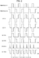
- FIG. 2 is a timing chart illustrating the operation of the insulation-type switching power supply according to the present invention.
- the transistor Q4 is in an on-state and the transistor Q5 is in an off-state.
- the PWM pulse 2 is at the low level (0 V)
- the transistor Q6 is in the off-state and the transistor Q7 is in the on-state.
- the voltage (L22 V (pulse transformer output voltage 1)) of the winding start of the first secondary winding L22 in the pulse transformer 21 becomes a positive pulse voltage.
- the voltage (L23 V (pulse transformer output voltage 2)) of the winding end of the second secondary winding L23 in the pulse transformer 21 becomes a negative pulse voltage.
- the transistors Q4, Q6 are in the off-state and the transistors Q5, Q7 are in the on-state.
- the excitation current does not flow in the primary winding L21 of the pulse transformer 21.
- the transistor Q6 is in the on-state and the transistor Q7 is in the off-state.
- the PWM pulse 1 is at the low level (0 V)
- the transistor Q4 is in the off-state and the transistor Q5 is in the on-state.
- the primary winding L21 of the pulse transformer 21 the excitation current flows from the winding start to the winding end, and the primary winding L21 is excited in the reverse direction.
- the voltage of the winding start of the first secondary winding L22 in the pulse transformer 21 becomes a negative pulse voltage.
- the voltage of the winding end of the second secondary winding L23 in the pulse transformer 21 becomes a positive pulse voltage.
- the transistors Q4, Q6 are in the off-state and the transistors Q5, Q7 are in the on-state.
- the excitation current does not flow in the primary winding L21 of the pulse transformer 21.
- the PWM Pulse 1 While the PWM Pulse 1 is at the high level (timing T1 to T2), in the first rectifier circuit 231, a current flows in the first rectifier diode D2.
- the PWM pulse 2 is at the high level (timing T3 to T4), the direction of the current flowing in the first secondary winding L22 is the reverse direction, so that the current does not flow in the first rectifier diode D2. That is, the first rectifier diode D2 half-wave rectifies a pulse signal (L22 V (pulse transformer output voltage 1)) induced at the winding start of the first secondary winding L22 of the pulse transformer 21. Thereby, the same pulse signal as the PWM Pulse 1 is obtained (the collector-emitter voltage (VCE) of the transistor Q2).
- VCE collector-emitter voltage
- the PWM Pulse 2 is at the high level (timing T3 to T4), in the second rectifier circuit 232, a current flows in the second rectifier diode D3.
- the PWM pulse 1 is at the high level (timing T1 to T2)
- the direction of the current flowing in the second secondary winding L23 is the reverse direction, so that the current does not flow in the second rectifier diode D3. That is, the second rectifier diode D3 half-wave rectifies a pulse signal (L23 V (pulse transformer output voltage 2)) induced at the winding end of the second secondary winding L23 of the pulse transformer 21.
- the same pulse signal as the PWM pulse 2 is obtained (the collector-emitter voltage (VCE) of the transistor Q3).
- a pulse signal to be the logical sum of the output signal of the first rectifier diode D2 and the output signal of the second rectifier diode D3 is generated. That is, a pulse signal, obtained by inverting a negative pulse of a pulse signal induced in the first secondary winding L22 of the pulse transformer 21 to a positive pulse, is generated (the gate-source voltage (VGS) of the field-effect transistor Q1). Thereby, the same pulse signal as the PWM control pulse signal generated by the PWM control circuit 25 is obtained.
- VGS gate-source voltage
- the transistor Q2 is in the off-state and the transistor Q3 is in the on-state.
- the gate of the field-effect transistor Q1 is thus not connected to the primary-side ground GND1.
- the transistor Q2 is in the on-state and the transistor Q3 is in the off-state.
- the gate of the field-effect transistor Q1 is thus not connected to the primary-side ground GND1.
- the transistors Q2, Q3 are both in the on-state.
- the gate of the field-effect transistor Q1 is connected to the primary-side ground GND1, and the charge of the gate of the field-effect transistor Q1 is drawn (a collector current Ic of the transistors Q2, Q3).
- the insulation-type switching power supply since the primary winding L21 of the pulse transformer 21 is alternately excited in the bidirectional manner using the first PWM pulse 1 and the second PWM pulse 2, a reset circuit for the pulse transformer 21 is not required, and even when the PWM control pulse signal generated by the PWM control circuit 25 has a switching duty ratio beyond 50%, magnetic saturation, reverse electromotive voltage, or the like does not occur in the pulse transformer 21. Therefore, according to the present invention, it is possible to provide, at low cost, an insulation-type switching power supply that can operate at a switching duty ratio beyond 50% and has a small size and high efficiency.
- the configuration of the switching circuit 23 of the embodiment is a simple circuit configuration using two half-wave rectifier circuits (first rectifier circuit 231, second rectifier circuit 232) and is thus preferred in terms of being able to provide the insulation-type switching power supply according to the present invention at lower cost. Further, the configuration of the switching circuit 23 of the embodiment is an extremely simple circuit configuration using two rectifier diodes (first rectifier diode D2, second rectifier diode D3) and is thus preferred in terms of being able to provide the insulation-type switching power supply according to the present invention at even lower cost.
- the insulation-type switching power supply according to the present invention is preferably provided with the drawing circuit 233 that draws the charge of the gate of the field-effect transistor Q1 while the input signal of the first rectifier circuit 231 and the input signal of the second rectifier circuit 232 are both at the low level.
- the drawing circuit 233 draws the charge of the gate of the field-effect transistor Q1 while the PWM control pulse signal is at the low level.
- the drawing circuit 233 of the embodiment has a simple circuit configuration that turns on and off two PNP transistors (transistors Q2, Q3) by using signals induced in the first secondary winding L22 and the second secondary winding L23 of the pulse transformer 21 and is thus preferred in terms of being able to provide the insulation-type switching power supply according to the present invention at even lower cost.
- the drawing circuit 233 is preferably provided with the resistors R3, R4 that limit the base currents of the transistors Q2, Q3. By adjusting the resistance values of the resistors R3, R4, it is possible to adjust the operation timings of the transistors Q2, Q3 so that the charge of the gate of the field-effect transistor Q1 is withdrawn at an accurate timing.
- a first aspect of the present invention is an insulation-type switching power supply including: a flyback converter circuit; and a feedback control circuit that performs pulse width modulation (PWM) control of a switching element in the flyback converter circuit based on an output voltage of the flyback converter circuit.
- PWM pulse width modulation
- the feedback control circuit includes a PWM control circuit that generates and outputs a first PWM control pulse signal and a second PWM control pulse signal respectively by alternately extracting pulses of a PWM control pulse signal of the switching element, a transformer, a bidirectional excitation circuit that excites a primary winding of the transformer in a forward direction using the first PWM control pulse signal and excites the primary winding of the transformer in a reverse direction using the second PWM control pulse signal, and a switching circuit that generates a pulse signal by inverting a negative pulse of a pulse signal, induced in a secondary winding of the transformer, to a positive pulse and switches the switching element by using the generated pulse signal.
- a first PWM control pulse signal and a second PWM control pulse signal are generated by alternately extracting pulses of the PWM control pulse signal, and the primary winding of the transformer is alternately excited in a bidirectional manner using the first PWM control pulse signal and the second PWM control pulse signal. Then, a pulse signal is generated by inverting a negative pulse of a pulse signal, induced in the secondary winding of the transformer, to a positive pulse, so that the same pulse signal as the PWM control pulse signal generated by the PWM control circuit is obtained.
- the PWM control pulse signal generated by the PWM control circuit on the secondary side (output side) of the flyback converter circuit, is transmitted to the primary side (input side) of the flyback converter circuit via the transformer to enable the feedback control of the flyback converter circuit.
- the primary winding of the transformer is alternately excited in the bidirectional manner using the first PWM control pulse signal and the second PWM control pulse signal, a reset circuit for the transformer is not required, and even when the PWM control pulse signal has a switching duty ratio beyond 50%, magnetic saturation, reverse electromotive voltage, or the like does not occur in the transformer.
- the first aspect of the present invention it is possible to provide, at low cost, an insulation-type switching power supply that can operate at a switching duty ratio beyond 50% and has a small size and high efficiency.
- a second aspect of the present invention is, in the first aspect of the present invention described above, an insulation-type switching power supply in which the secondary winding of the transformer includes a first secondary winding and a second secondary winding, the switching circuit includes a first rectifier circuit that half-wave rectifies and outputs a pulse signal induced in the first secondary winding, and a second rectifier circuit that half-wave rectifies and outputs a pulse signal obtained by reversing a polarity of a pulse signal induced in the second secondary winding, and the switching circuit generates a pulse signal to be a logical sum of an output signal of the first rectifier circuit and an output signal of the second rectifier circuit, and switches the switching element by using the generated pulse signal.
- a pulse signal induced in the first secondary winding is half-wave rectified to obtain the same pulse signal as the first PWM control pulse signal.
- a pulse signal obtained by inverting the polarity of a pulse signal induced in the second secondary winding, is half-wave rectified to obtain the same pulse signal as the second PWM control pulse signal. Then, a pulse signal to be the logical sum of the output signal of the first rectifier circuit and the output signal of the second rectifier circuit is generated to obtain the same pulse signal as the PWM control pulse signal generated by the PWM control circuit.
- the same pulse signal as the PWM control pulse signal generated by the PWM control circuit is obtained by the switching circuit with a simple circuit configuration using two half-wave rectifier circuits, so that it is possible to provide the insulation-type switching power supply according to the present invention at lower cost.
- a third aspect of the present invention is, in the second aspect of the present invention described above, an insulation-type switching power supply in which in the transformer, a winding end of the first secondary winding and a winding start of the second secondary winding are connected to a ground terminal of the switching element, the first rectifier circuit includes a first rectifier diode having an anode connected to a winding start of the first secondary winding and a cathode connected to a control terminal of the switching element, and the second rectifier circuit includes a second rectifier diode having an anode connected to a winding end of the second secondary winding and a cathode connected to the control terminal of the switching element.
- the same pulse signal as the PWM control pulse signal generated by the PWM control circuit is obtained by the rectifier circuit with an extremely simple circuit configuration using two rectifier diodes, so that it is possible to provide the insulation-type switching power supply according to the present invention at even lower cost.
- a fourth aspect of the present invention is, in the second or third aspect of the present invention described above, an insulation-type switching power supply in which the feedback control circuit further includes a drawing circuit that draws a charge of the control terminal of the switching element while an input signal of the first rectifier circuit and an input signal of the second rectifier circuit are both at a low level.
- the first PWM control pulse signal and the second PWM control pulse signal are both at the low level, that is, the PWM control pulse signal is at the low level.
- a fifth aspect of the present invention is, in the fourth aspect of the present invention described above, an insulation-type switching power supply in which the drawing circuit includes a first PNP transistor having a base connected to the winding start of the first secondary winding and an emitter connected to the control terminal of the switching element, and a second PNP transistor having a base connected to the winding end of the second secondary winding, an emitter connected to a collector of the first PNP transistor, and a collector connected to the ground terminal of the switching element.
- the drawing circuit with such a configuration only while the PWM control pulse signal is at the low level, the first PNP transistor and the second PNP transistor are both in the on-state, and the control terminal of the switching element is connected to the ground terminal of the switching element. Thereby, while the PWM control pulse signal is at the low level, it is possible to draw the charge of the control terminal of the switching element.
- the insulation-type switching power supply according to the present invention at even lower cost due to the drawing circuit with a simple circuit configuration that turns on and off two PNP transistors by using signals induced in the first secondary winding and the second secondary winding of the transformer.
- a sixth aspect of the present invention is, in the fifth aspect of the present invention described above, an insulation-type switching power supply in which in the drawing circuit, current-limiting resistors are respectively provided between the winding start of the first secondary winding and the base of the first PNP transistor and between the winding end of the second secondary winding and the base of the second PNP transistor.
- the sixth aspect of the present invention by adjusting the resistance values of the current-limiting resistors, it is possible to adjust the operation timings of the first PNP transistor and the second PNP transistor so that the charge of the control terminal of the switching element is withdrawn at an accurate timing.
- a seventh aspect of the present invention is, in the fourth aspect of the present invention described above, an insulation-type switching power supply in which the drawing circuit includes a first PNP transistor having a base connected to the winding end of the second secondary winding and an emitter connected to the control terminal of the switching element, and a second PNP transistor having a base connected to the winding start of the first secondary winding, an emitter connected to a collector of the first PNP transistor, and a collector connected to the ground terminal of the switching element.
- the seventh aspect of the present invention similarly to the fifth aspect of the present invention, it is possible to provide the insulation-type switching power supply according to the present invention at even lower cost due to the drawing circuit with a simple circuit configuration that turns on and off two PNP transistors by using signals induced in the first secondary winding and the second secondary winding of the transformer.
- An eighth aspect of the present invention is, in the seventh aspect of the present invention described above, an insulation-type switching power supply in which in the drawing circuit, current-limiting resistors are respectively provided between the winding start of the first secondary winding and the base of the second PNP transistor and between the winding end of the second secondary winding and the base of the first PNP transistor.
- the eighth aspect of the present invention similarly to the sixth aspect of the present invention, by adjusting the resistance values of the current-limiting resistors, it is possible to adjust the operation timings of the first PNP transistor and the second PNP transistor so that the charge of the control terminal of the switching element is withdrawn at an accurate timing.
- a ninth aspect of the present invention is, in the fourth aspect of the present invention described above, an insulation-type switching power supply in which the drawing circuit includes a first p-channel field-effect transistor having a gate connected to the winding start of the first secondary winding and a source connected to the control terminal of the switching element, and a second p-channel field-effect transistor having a gate connected to the winding end of the second secondary winding, a source connected to a drain of the first p-channel field-effect transistor, and a drain connected to the ground terminal of the switching element.
- the ninth aspect of the present invention similarly to the fifth aspect of the present invention, it is possible to provide the insulation-type switching power supply according to the present invention at even lower cost due to the drawing circuit with a simple circuit configuration that turns on and off two p-channel field-effect transistors by using signals induced in the first secondary winding and the second secondary winding of the transformer.
- a tenth aspect of the present invention is, in the ninth aspect of the present invention described above, an insulation-type switching power supply in which in the drawing circuit, current-limiting resistors are respectively provided between the winding start of the first secondary winding and the gate of the first p-channel field-effect transistor and between the winding end of the second secondary winding and the gate of the second p-channel field-effect transistor.
- the tenth aspect of the present invention similarly to the sixth aspect of the present invention, by adjusting the resistance values of the current-limiting resistors, it is possible to adjust the operation timings of the first p-channel field-effect transistor and the second p-channel field-effect transistor so that the charge of the control terminal of the switching element is withdrawn at an accurate timing.
- An eleventh aspect of the present invention is, in the fourth aspect of the present invention described above, an insulation-type switching power supply in which the drawing circuit includes a first p-channel field-effect transistor having a gate connected to the winding end of the second secondary winding and a source connected to the control terminal of the switching element, and a second p-channel field-effect transistor having a gate connected to the winding start of the first secondary winding, a source connected to a drain of the first p-channel field-effect transistor, and a drain connected to the ground terminal of the switching element.
- the eleventh aspect of the present invention similarly to the fifth aspect of the present invention, it is possible to provide the insulation-type switching power supply according to the present invention at even lower cost due to the drawing circuit with a simple circuit configuration that turns on and off two p-channel field-effect transistor by using signals induced in the first secondary winding and the second secondary winding of the transformer.
- a twelfth aspect of the present invention is, in the eleventh aspect of the present invention described above, an insulation-type switching power supply in which in the drawing circuit, current-limiting resistors are respectively provided between the winding start of the first secondary winding and the gate of the second p-channel field-effect transistor and between the winding end of the second secondary winding and the gate of the first p-channel field-effect transistor.
Landscapes
- Engineering & Computer Science (AREA)
- Power Engineering (AREA)
- Dc-Dc Converters (AREA)
Abstract
Description
- The present invention relates to an insulation-type switching power supply provided with a flyback converter circuit.
- For performing constant voltage control of an output voltage, a conventional insulation-type switching power supply provided with a flyback converter circuit feeds back an output voltage on the secondary side to the primary side via an insulating circuit such as a photocoupler or a transformer and controls a switching duty ratio of a switching element of the flyback converter circuit in a pulse width modulation (PWM) control circuit provided on the primary side (e.g., see
Patent Document 1 or 2) . -
- Patent Document 1: Japanese Patent Laid-Open No.
08-033341 - Patent Document 2: Japanese Patent Laid-Open No.
2007-020395 - However, since the above prior art is configured to have the PWM control circuit provided on the primary side, it is necessary to separately provide a constant voltage power supply for the PWM control circuit on the primary side where a high voltage is often handled, thereby causing a problem of difficulty in reducing the size and cost of the circuit. Hence it is conceivable that the PWM control circuit is provided on the secondary side, and a PWM control pulse is transmitted to the primary side via the transformer.
- However, when the PWM control circuit is provided on the secondary side and the PWM control pulse is transmitted to the primary side via the transformer, a reset circuit for resetting the transformer is required. Further, when the switching duty ratio of the PWM control pulse exceeds 50%, there is a risk that the reset circuit may not be able to reset the transformer, and magnetic saturation, a reverse electromotive voltage, or the like may occur to cause damage on a peripheral circuit or the like. In this case, such a risk of the occurrence of the magnetic saturation, the reverse electromotive voltage, or the like can be reduced by, for example, increasing the size of the transformer and a semiconductor element which transmit the PWM control pulse to the primary side. However, there is also a risk that the use of a large-sized transformer or the like may make it difficult to reduce the size and cost of the circuit and may cause an increase in loss and a decrease in power conversion efficiency. On the other hand, when the switching duty ratio of the PWM control pulse is limited up to 50% so as to avoid such a situation as thus described, it is impossible to take advantage of the flyback converter circuit which is operable at a switching duty ratio beyond 50%.
- The present invention has been made in view of such circumstances, and an object of the present invention is to provide, at low cost, an insulation-type switching power supply that can operate at a switching duty ratio beyond 50% and has a small size and high efficiency.
- An aspect of the present invention is an insulation-type switching power supply including: a flyback converter circuit; and a feedback control circuit that performs pulse width modulation (PWM) control of a switching element in the flyback converter circuit based on an output voltage of the flyback converter circuit. The feedback control circuit includes a PWM control circuit that generates and outputs a first PWM control pulse signal and a second PWM control pulse signal respectively by alternately extracting pulses of a PWM control pulse signal of the switching element, a transformer, a bidirectional excitation circuit that excites a primary winding of the transformer in a forward direction using the first PWM control pulse signal and excites the primary winding of the transformer in a reverse direction using the second PWM control pulse signal, and a switching circuit that generates a pulse signal by inverting a negative pulse of a pulse signal, induced in a secondary winding of the transformer, to a positive pulse and switches the switching element by using the generated pulse signal.
- As thus described, a first PWM control pulse signal and a second PWM control pulse signal are generated by alternately extracting pulses of the PWM control pulse signal, and the primary winding of the transformer is alternately excited in a bidirectional manner using the first PWM control pulse signal and the second PWM control pulse signal. Then, a pulse signal is generated by inverting a negative pulse of a pulse signal, induced in the secondary winding of the transformer, to a positive pulse, so that the same pulse signal as the PWM control pulse signal generated by the PWM control circuit is obtained. Thereby, the PWM control pulse signal, generated by the PWM control circuit on the secondary side (output side) of the flyback converter circuit, is transmitted to the primary side (input side) of the flyback converter circuit via the transformer to enable the feedback control of the flyback converter circuit. In the present invention, since the primary winding of the transformer is alternately excited in the bidirectional manner using the first PWM control pulse signal and the second PWM control pulse signal, a reset circuit for the transformer is not required, and even when the PWM control pulse signal has a switching duty ratio beyond 50%, magnetic saturation, reverse electromotive voltage, or the like does not occur in the transformer.
- Therefore, according to the aspect of the present invention, it is possible to provide, at low cost, an insulation-type switching power supply that can operate at a switching duty ratio beyond 50% and has a small size and high efficiency.
- According to the present invention, it is possible to provide, at low cost, an insulation-type switching power supply that can operate at a switching duty ratio beyond 50% and has a small size and high efficiency.
-
-
FIG. 1 is a circuit diagram of an insulation-type switching power supply according to the present invention. -
FIG. 2 is a timing chart illustrating the operation of the insulation-type switching power supply according to the present invention. - Hereinafter, the embodiment of the present invention will be described with reference to the accompanying drawings. The present invention is not particularly limited to the embodiment described below, but needless to say, various modifications are possible within the scope of the invention described in the claims.
- The configuration of the insulation-type switching power supply according to the present invention will be described with reference to
FIG. 1 . -
FIG. 1 is a circuit diagram of an insulation-type switching power supply according to the present invention. - The insulation-type switching power supply according to the present invention is provided with a
flyback converter circuit 10 and afeedback control circuit 20. - The
flyback converter circuit 10 is a flyback insulation-type DC-DC converter and includes an insulating transformer T1, a field-effect transistor Q1, resistors R1, R2, capacitors C1, C2, and a diode D1. - The insulating transformer T1 includes a primary winding L11 and secondary winding L12. The winding start of the primary winding L11 of the insulating transformer T1 is connected to an input Vin, and the winding end of the primary winding L11 is connected to the drain of the field-effect transistor Q1. Each of the resistor R1 and the resistor R2 has one end connected to the gate (control terminal) of the field-effect transistor Q1. The other end of the resistor R1 is connected to the
feedback control circuit 20. The other end of the resistor R2 is connected to a primary-side ground GND1. One end of the capacitor C1 is connected to the input Vin, and the other end of the capacitor C1 is connected to the primary-side ground GND1. The source of the field-effect transistor Q1 is connected to the primary-side ground GND1. - The winding start of the secondary winding L12 of the insulating transformer T1 is connected to a secondary-side ground GND2, and the winding end of the secondary winding L12 is connected to the anode of the diode D1. The cathode of the diode D1 is connected to an output Vout. One end of the capacitor C2 is connected to the output Vout, and the other end of the capacitor C2 is connected to the secondary-side ground GND2.
- In the
flyback converter circuit 10 with such a configuration, power is stored into the insulating transformer T1 while the field-effect transistor Q1 as a "switching element" is on. Then, at the timing of turning-off of the field-effect transistor Q1, the power stored in the insulating transformer T1 is output by the counter electromotive force of the insulating transformer T1. - The
feedback control circuit 20 performs the PWM control of the field-effect transistor Q1 in theflyback converter circuit 10 based on the voltage of the output Vout of theflyback converter circuit 10. Thefeedback control circuit 20 includes apulse transformer 21, abidirectional excitation circuit 22, aswitching circuit 23, adriver 24, and thePWM control circuit 25. - The
pulse transformer 21 as a "transformer" includes a primary winding L21, a first secondary winding L22, and a second secondary winding L23. The winding end of the first secondary winding L22 and the winding start of the second secondary winding L23 are connected to the primary-side ground GND1. - The
bidirectional excitation circuit 22 is a circuit that excites the primary winding L21 of thepulse transformer 21 in the forward direction using thePWM pulse 1 generated by thePWM control circuit 25 and excites the primary winding L21 of thepulse transformer 21 in the reverse direction using thePWM pulse 2, as described later. Thebidirectional excitation circuit 22 includes transistors Q4 to Q7 and capacitors C3, C4. The transistors Q4, Q6 are NPN bipolar transistors, and the transistors Q5, Q7 are PNP bipolar transistors. - The collector of the transistor Q4 is connected to an output Vcc of a constant voltage power supply for control (not illustrated). The emitter of the transistor Q4 is connected to the emitter of the transistor Q5. The collector of the transistor Q5 is connected to the secondary-side ground GND2. The base of the transistor Q4 is connected to the base of the transistor Q5, and the point of the connection is connected to the
driver 24. The point of connection between the emitter of the transistor Q4 and the emitter of the transistor Q5 is connected to one end of the capacitor C3. The other end of the capacitor C3 is connected to the winding start of the primary winding L21 of thepulse transformer 21. - The collector of the transistor Q6 is connected to the output Vcc. The emitter of the transistor Q6 is connected to the emitter of the transistor Q7. The collector of the transistor Q7 is connected to the secondary-side ground GND2. The base of the transistor Q6 is connected to the base of the transistor Q7, and the point of the connection is connected to the
driver 24. The point of connection between the emitter of the transistor Q6 and the emitter of the transistor Q7 is connected to the winding end of the primary winding L21 of thepulse transformer 21. One end of the capacitor C4 is connected to the output Vcc, and the other end of the capacitor C4 is connected to the secondary-side ground GND2. - The switching
circuit 23 generates a pulse signal by removing a negative pulse of a pulse signal induced in each of the first secondary winding L22 and the second secondary winding L23 of thepulse transformer 21 and synthesizing a positive pulse, that is, generates a pulse signal by inverting a negative pulse of a pulse signal, induced in the secondary winding of thetransformer 21, to a positive pulse, and switches the field-effect transistor Q1 by using the generated pulse signal. Thereby, the PWM control pulse signal, generated by thePWM control circuit 25 on the secondary side (output Vout side) of theflyback converter circuit 10, is transmitted to the primary side (input Vin side) of theflyback converter circuit 10 via thepulse transformer 21 to enable the feedback control of theflyback converter circuit 10. The switchingcircuit 23 includes afirst rectifier circuit 231, asecond rectifier circuit 232, and adrawing circuit 233. - The
first rectifier circuit 231 is a circuit for half-wave rectifying and outputting a pulse signal induced in the first secondary winding L22, and thefirst rectifier circuit 231 includes a first rectifier diode D2. Thesecond rectifier circuit 232 is a circuit for half-wave rectifying and outputting a pulse signal, obtained by inverting the polarity of a pulse signal induced in the second secondary winding L23, and thesecond rectifier circuit 232 includes a second rectifier diode D3. The type of each of the first rectifier diode D2 and the second rectifier diode D3 is not particularly limited so long as being a diode capable of half-wave rectifying a pulse signal, but it is preferable to use a Schottky barrier diode having excellent switching characteristics as in the embodiment. - The anode of the first rectifier diode D2 is connected to the winding start of the first secondary winding L22 of the
pulse transformer 21. The anode of the second rectifier diode D3 is connected to the winding end of the second secondary winding L23 of thepulse transformer 21. The cathode of each of the first rectifier diode D2 and the second rectifier diode D3 is connected to the gate of the field-effect transistor Q1 via the resistor R1 of theflyback converter circuit 10. Thereby, a pulse signal to be the logical sum of the output signal of thefirst rectifier circuit 231 and the output signal of thesecond rectifier circuit 232 is generated, and the field-effect transistor Q1 is switched using the generated pulse signal. - The
drawing circuit 233 is a circuit for drawing the charge of the gate of the field-effect transistor Q1 while the input signal of thefirst rectifier circuit 231 and the input signal of thesecond rectifier circuit 232 are both at the low level. Thedrawing circuit 233 includes transistors Q2, Q3 and resistors R3, R4. - The transistor Q2 as a "first PNP transistor" and the transistor Q3 as a "second PNP transistor" are, for example, PNP bipolar transistors. The base of the transistor Q2 is connected to the winding start of the first secondary winding L22, and the emitter of the transistor Q2 is connected to the gate of the field-effect transistor Q1. The base of the transistor Q3 is connected to the winding end of the second secondary winding L23, and the collector of the transistor Q3 is connected to the primary-side ground GND1. The collector of the transistor Q2 is connected to the emitter of the transistor Q3.
- The resistor R3 as a "current-limiting resistor" is a resistor that limits the base current of the transistor Q2. One end of the resistor R3 is connected to the winding start of the first secondary winding L22, and the other end of the resistor R3 is connected to the base of the transistor Q2. The resistor R4 as the "current-limiting resistor" is a resistor that limits the base current of the transistor Q3. One end of the resistor R4 is connected to the winding end of the second secondary winding L23, and the other end of the resistor R4 is connected to the base of the transistor Q3.
- Though not illustrated, as a modification of the present invention, the base of the transistor Q2 of the
drawing circuit 233 may be connected to the winding end of the second secondary winding L23 via the resistor R4, and the base of the transistor Q3 of thedrawing circuit 233 may be connected to the winding start of the first secondary winding L22 via the resistor R3. Further, as a modification of the present invention, the transistors Q2, Q3 may, for example, be p-channel field-effect transistors. - The
driver 24 drives the transistors Q4 to Q7 of thebidirectional excitation circuit 22 based on a control signal output by thePWM control circuit 25. ThePWM control circuit 25 is, for example, a known microcomputer control circuit or control integrated circuit (IC). Based on the voltage of the output Vout of theflyback converter circuit 10, thePWM control circuit 25 generates a PWM control pulse signal for switching the field-effect transistor Q1 and generates a PWM pulse 1 (first PWM control pulse signal) and a PWM pulse 2 (second PWM control pulse signal) respectively by alternately extracting pulses of the PWM control pulse signal, to output the generated pulses to thedriver 24. - The operation of the insulation-type switching power supply according to the present invention will be described with reference to
FIG. 2 . -
FIG. 2 is a timing chart illustrating the operation of the insulation-type switching power supply according to the present invention. - During the time when the
PWM pulse 1 is at the high level (timing T1 to T2), in thebidirectional excitation circuit 22, the transistor Q4 is in an on-state and the transistor Q5 is in an off-state. Further, since thePWM pulse 2 is at the low level (0 V), during that time, the transistor Q6 is in the off-state and the transistor Q7 is in the on-state. Hence in the primary winding L21 of thepulse transformer 21, an excitation current flows from the winding start to the winding end, and the primary winding L21 is excited in the forward direction. Thereby, the voltage (L22 V (pulse transformer output voltage 1)) of the winding start of the first secondary winding L22 in thepulse transformer 21 becomes a positive pulse voltage. On the other hand, the voltage (L23 V (pulse transformer output voltage 2)) of the winding end of the second secondary winding L23 in thepulse transformer 21 becomes a negative pulse voltage. - While the
PWM pulse 1 and thePWM pulse 2 are both at the low level after the shift of thePWM pulse 1 to the low level (timing T2 to T3), in thebidirectional excitation circuit 22, the transistors Q4, Q6 are in the off-state and the transistors Q5, Q7 are in the on-state. Hence the excitation current does not flow in the primary winding L21 of thepulse transformer 21. Thereby, the voltage of the winding start of the first secondary winding L22 in thepulse transformer 21 and the voltage of the winding end of the second secondary winding L23 in thepulse transformer 21 both become 0 V. - During the time when the
PWM pulse 2 is at the high level (timing T3 to T4), in thebidirectional excitation circuit 22, the transistor Q6 is in the on-state and the transistor Q7 is in the off-state. Further, since thePWM pulse 1 is at the low level (0 V), during that time, the transistor Q4 is in the off-state and the transistor Q5 is in the on-state. Hence in the primary winding L21 of thepulse transformer 21, the excitation current flows from the winding start to the winding end, and the primary winding L21 is excited in the reverse direction. Thereby, the voltage of the winding start of the first secondary winding L22 in thepulse transformer 21 becomes a negative pulse voltage. On the other hand, the voltage of the winding end of the second secondary winding L23 in thepulse transformer 21 becomes a positive pulse voltage. - While the
PWM pulse 1 and thePWM pulse 2 are both at the low level after the shift of thePWM pulse 2 to the low level (timing T4 to T1), in thebidirectional excitation circuit 22, the transistors Q4, Q6 are in the off-state and the transistors Q5, Q7 are in the on-state. Hence the excitation current does not flow in the primary winding L21 of thepulse transformer 21. Thereby, the voltage of the winding start of the first secondary winding L22 in thepulse transformer 21 and the voltage of the winding end of the second secondary winding L23 in thepulse transformer 21 both become 0 V. - While the
PWM Pulse 1 is at the high level (timing T1 to T2), in thefirst rectifier circuit 231, a current flows in the first rectifier diode D2. On the other hand, while thePWM pulse 2 is at the high level (timing T3 to T4), the direction of the current flowing in the first secondary winding L22 is the reverse direction, so that the current does not flow in the first rectifier diode D2. That is, the first rectifier diode D2 half-wave rectifies a pulse signal (L22 V (pulse transformer output voltage 1)) induced at the winding start of the first secondary winding L22 of thepulse transformer 21. Thereby, the same pulse signal as thePWM Pulse 1 is obtained (the collector-emitter voltage (VCE) of the transistor Q2). - While the
PWM Pulse 2 is at the high level (timing T3 to T4), in thesecond rectifier circuit 232, a current flows in the second rectifier diode D3. On the other hand, while thePWM pulse 1 is at the high level (timing T1 to T2), the direction of the current flowing in the second secondary winding L23 is the reverse direction, so that the current does not flow in the second rectifier diode D3. That is, the second rectifier diode D3 half-wave rectifies a pulse signal (L23 V (pulse transformer output voltage 2)) induced at the winding end of the second secondary winding L23 of thepulse transformer 21. Thereby, the same pulse signal as thePWM pulse 2 is obtained (the collector-emitter voltage (VCE) of the transistor Q3). - By the connection between the cathode of the first rectifier diode D2 and the cathode of the second rectifier diode D3, a pulse signal to be the logical sum of the output signal of the first rectifier diode D2 and the output signal of the second rectifier diode D3 is generated. That is, a pulse signal, obtained by inverting a negative pulse of a pulse signal induced in the first secondary winding L22 of the
pulse transformer 21 to a positive pulse, is generated (the gate-source voltage (VGS) of the field-effect transistor Q1). Thereby, the same pulse signal as the PWM control pulse signal generated by thePWM control circuit 25 is obtained. - During the time when the
PWM pulse 1 is at the high level (timing T1 to T2), in thedrawing circuit 233, the transistor Q2 is in the off-state and the transistor Q3 is in the on-state. The gate of the field-effect transistor Q1 is thus not connected to the primary-side ground GND1. Similarly, during the time when thePWM pulse 2 is at the high level (timing T3 to T4), the transistor Q2 is in the on-state and the transistor Q3 is in the off-state. The gate of the field-effect transistor Q1 is thus not connected to the primary-side ground GND1. On the other hand, during the time when thePWM pulse 1 and thePWM pulse 2 are both at the low level (timings T2 to T3, T4 to T1), in thedrawing circuit 233, the transistors Q2, Q3 are both in the on-state. Thereby, the gate of the field-effect transistor Q1 is connected to the primary-side ground GND1, and the charge of the gate of the field-effect transistor Q1 is drawn (a collector current Ic of the transistors Q2, Q3). - As described above, in the insulation-type switching power supply according to the present invention, since the primary winding L21 of the
pulse transformer 21 is alternately excited in the bidirectional manner using thefirst PWM pulse 1 and thesecond PWM pulse 2, a reset circuit for thepulse transformer 21 is not required, and even when the PWM control pulse signal generated by thePWM control circuit 25 has a switching duty ratio beyond 50%, magnetic saturation, reverse electromotive voltage, or the like does not occur in thepulse transformer 21.
Therefore, according to the present invention, it is possible to provide, at low cost, an insulation-type switching power supply that can operate at a switching duty ratio beyond 50% and has a small size and high efficiency. - The configuration of the switching
circuit 23 of the embodiment is a simple circuit configuration using two half-wave rectifier circuits (first rectifier circuit 231, second rectifier circuit 232) and is thus preferred in terms of being able to provide the insulation-type switching power supply according to the present invention at lower cost. Further, the configuration of the switchingcircuit 23 of the embodiment is an extremely simple circuit configuration using two rectifier diodes (first rectifier diode D2, second rectifier diode D3) and is thus preferred in terms of being able to provide the insulation-type switching power supply according to the present invention at even lower cost. - Moreover, as in the embodiment, the insulation-type switching power supply according to the present invention is preferably provided with the
drawing circuit 233 that draws the charge of the gate of the field-effect transistor Q1 while the input signal of thefirst rectifier circuit 231 and the input signal of thesecond rectifier circuit 232 are both at the low level. By drawing the charge of the gate of the field-effect transistor Q1 while the PWM control pulse signal is at the low level, the field-effect transistor Q1 can be stably switched at a more accurate timing, to enable highly accurate PWM control. - Further, the
drawing circuit 233 of the embodiment has a simple circuit configuration that turns on and off two PNP transistors (transistors Q2, Q3) by using signals induced in the first secondary winding L22 and the second secondary winding L23 of thepulse transformer 21 and is thus preferred in terms of being able to provide the insulation-type switching power supply according to the present invention at even lower cost. Moreover, as in the embodiment, thedrawing circuit 233 is preferably provided with the resistors R3, R4 that limit the base currents of the transistors Q2, Q3. By adjusting the resistance values of the resistors R3, R4, it is possible to adjust the operation timings of the transistors Q2, Q3 so that the charge of the gate of the field-effect transistor Q1 is withdrawn at an accurate timing. - A first aspect of the present invention is an insulation-type switching power supply including: a flyback converter circuit; and a feedback control circuit that performs pulse width modulation (PWM) control of a switching element in the flyback converter circuit based on an output voltage of the flyback converter circuit. The feedback control circuit includes a PWM control circuit that generates and outputs a first PWM control pulse signal and a second PWM control pulse signal respectively by alternately extracting pulses of a PWM control pulse signal of the switching element, a transformer, a bidirectional excitation circuit that excites a primary winding of the transformer in a forward direction using the first PWM control pulse signal and excites the primary winding of the transformer in a reverse direction using the second PWM control pulse signal, and a switching circuit that generates a pulse signal by inverting a negative pulse of a pulse signal, induced in a secondary winding of the transformer, to a positive pulse and switches the switching element by using the generated pulse signal.
- As thus described, a first PWM control pulse signal and a second PWM control pulse signal are generated by alternately extracting pulses of the PWM control pulse signal, and the primary winding of the transformer is alternately excited in a bidirectional manner using the first PWM control pulse signal and the second PWM control pulse signal. Then, a pulse signal is generated by inverting a negative pulse of a pulse signal, induced in the secondary winding of the transformer, to a positive pulse, so that the same pulse signal as the PWM control pulse signal generated by the PWM control circuit is obtained. Thereby, the PWM control pulse signal, generated by the PWM control circuit on the secondary side (output side) of the flyback converter circuit, is transmitted to the primary side (input side) of the flyback converter circuit via the transformer to enable the feedback control of the flyback converter circuit. In the present invention, since the primary winding of the transformer is alternately excited in the bidirectional manner using the first PWM control pulse signal and the second PWM control pulse signal, a reset circuit for the transformer is not required, and even when the PWM control pulse signal has a switching duty ratio beyond 50%, magnetic saturation, reverse electromotive voltage, or the like does not occur in the transformer.
- Therefore, according to the first aspect of the present invention, it is possible to provide, at low cost, an insulation-type switching power supply that can operate at a switching duty ratio beyond 50% and has a small size and high efficiency.
- A second aspect of the present invention is, in the first aspect of the present invention described above, an insulation-type switching power supply in which the secondary winding of the transformer includes a first secondary winding and a second secondary winding, the switching circuit includes a first rectifier circuit that half-wave rectifies and outputs a pulse signal induced in the first secondary winding, and a second rectifier circuit that half-wave rectifies and outputs a pulse signal obtained by reversing a polarity of a pulse signal induced in the second secondary winding, and the switching circuit generates a pulse signal to be a logical sum of an output signal of the first rectifier circuit and an output signal of the second rectifier circuit, and switches the switching element by using the generated pulse signal.
- In the first rectifier circuit, a pulse signal induced in the first secondary winding is half-wave rectified to obtain the same pulse signal as the first PWM control pulse signal. In the second rectifier circuit, a pulse signal, obtained by inverting the polarity of a pulse signal induced in the second secondary winding, is half-wave rectified to obtain the same pulse signal as the second PWM control pulse signal. Then, a pulse signal to be the logical sum of the output signal of the first rectifier circuit and the output signal of the second rectifier circuit is generated to obtain the same pulse signal as the PWM control pulse signal generated by the PWM control circuit.
- Thereby, according to the second aspect of the present invention, the same pulse signal as the PWM control pulse signal generated by the PWM control circuit is obtained by the switching circuit with a simple circuit configuration using two half-wave rectifier circuits, so that it is possible to provide the insulation-type switching power supply according to the present invention at lower cost.
- A third aspect of the present invention is, in the second aspect of the present invention described above, an insulation-type switching power supply in which in the transformer, a winding end of the first secondary winding and a winding start of the second secondary winding are connected to a ground terminal of the switching element, the first rectifier circuit includes a first rectifier diode having an anode connected to a winding start of the first secondary winding and a cathode connected to a control terminal of the switching element, and the second rectifier circuit includes a second rectifier diode having an anode connected to a winding end of the second secondary winding and a cathode connected to the control terminal of the switching element.
- According to the third aspect of the present invention, the same pulse signal as the PWM control pulse signal generated by the PWM control circuit is obtained by the rectifier circuit with an extremely simple circuit configuration using two rectifier diodes, so that it is possible to provide the insulation-type switching power supply according to the present invention at even lower cost.
- A fourth aspect of the present invention is, in the second or third aspect of the present invention described above, an insulation-type switching power supply in which the feedback control circuit further includes a drawing circuit that draws a charge of the control terminal of the switching element while an input signal of the first rectifier circuit and an input signal of the second rectifier circuit are both at a low level.
- While the input signal of the first rectifier circuit and the input signal of the second rectifier circuit are both at the low level, the first PWM control pulse signal and the second PWM control pulse signal are both at the low level, that is, the PWM control pulse signal is at the low level. By drawing the charge of the control terminal of the switching element while the PWM control pulse signal is at the low level, the switching element can be stably switched at a more accurate timing, to enable highly accurate PWM control.
- A fifth aspect of the present invention is, in the fourth aspect of the present invention described above, an insulation-type switching power supply in which the drawing circuit includes a first PNP transistor having a base connected to the winding start of the first secondary winding and an emitter connected to the control terminal of the switching element, and a second PNP transistor having a base connected to the winding end of the second secondary winding, an emitter connected to a collector of the first PNP transistor, and a collector connected to the ground terminal of the switching element.
- In the drawing circuit with such a configuration, only while the PWM control pulse signal is at the low level, the first PNP transistor and the second PNP transistor are both in the on-state, and the control terminal of the switching element is connected to the ground terminal of the switching element. Thereby, while the PWM control pulse signal is at the low level, it is possible to draw the charge of the control terminal of the switching element. According to the fifth aspect of the present invention, it is possible to provide the insulation-type switching power supply according to the present invention at even lower cost due to the drawing circuit with a simple circuit configuration that turns on and off two PNP transistors by using signals induced in the first secondary winding and the second secondary winding of the transformer.
- A sixth aspect of the present invention is, in the fifth aspect of the present invention described above, an insulation-type switching power supply in which in the drawing circuit, current-limiting resistors are respectively provided between the winding start of the first secondary winding and the base of the first PNP transistor and between the winding end of the second secondary winding and the base of the second PNP transistor.
- According to the sixth aspect of the present invention, by adjusting the resistance values of the current-limiting resistors, it is possible to adjust the operation timings of the first PNP transistor and the second PNP transistor so that the charge of the control terminal of the switching element is withdrawn at an accurate timing.
- A seventh aspect of the present invention is, in the fourth aspect of the present invention described above, an insulation-type switching power supply in which the drawing circuit includes a first PNP transistor having a base connected to the winding end of the second secondary winding and an emitter connected to the control terminal of the switching element, and a second PNP transistor having a base connected to the winding start of the first secondary winding, an emitter connected to a collector of the first PNP transistor, and a collector connected to the ground terminal of the switching element.
- According to the seventh aspect of the present invention, similarly to the fifth aspect of the present invention, it is possible to provide the insulation-type switching power supply according to the present invention at even lower cost due to the drawing circuit with a simple circuit configuration that turns on and off two PNP transistors by using signals induced in the first secondary winding and the second secondary winding of the transformer.
- An eighth aspect of the present invention is, in the seventh aspect of the present invention described above, an insulation-type switching power supply in which in the drawing circuit, current-limiting resistors are respectively provided between the winding start of the first secondary winding and the base of the second PNP transistor and between the winding end of the second secondary winding and the base of the first PNP transistor.
- According to the eighth aspect of the present invention, similarly to the sixth aspect of the present invention, by adjusting the resistance values of the current-limiting resistors, it is possible to adjust the operation timings of the first PNP transistor and the second PNP transistor so that the charge of the control terminal of the switching element is withdrawn at an accurate timing.
- A ninth aspect of the present invention is, in the fourth aspect of the present invention described above, an insulation-type switching power supply in which the drawing circuit includes a first p-channel field-effect transistor having a gate connected to the winding start of the first secondary winding and a source connected to the control terminal of the switching element, and a second p-channel field-effect transistor having a gate connected to the winding end of the second secondary winding, a source connected to a drain of the first p-channel field-effect transistor, and a drain connected to the ground terminal of the switching element.
- According to the ninth aspect of the present invention, similarly to the fifth aspect of the present invention, it is possible to provide the insulation-type switching power supply according to the present invention at even lower cost due to the drawing circuit with a simple circuit configuration that turns on and off two p-channel field-effect transistors by using signals induced in the first secondary winding and the second secondary winding of the transformer.
- A tenth aspect of the present invention is, in the ninth aspect of the present invention described above, an insulation-type switching power supply in which in the drawing circuit, current-limiting resistors are respectively provided between the winding start of the first secondary winding and the gate of the first p-channel field-effect transistor and between the winding end of the second secondary winding and the gate of the second p-channel field-effect transistor.
- According to the tenth aspect of the present invention, similarly to the sixth aspect of the present invention, by adjusting the resistance values of the current-limiting resistors, it is possible to adjust the operation timings of the first p-channel field-effect transistor and the second p-channel field-effect transistor so that the charge of the control terminal of the switching element is withdrawn at an accurate timing.
- An eleventh aspect of the present invention is, in the fourth aspect of the present invention described above, an insulation-type switching power supply in which the drawing circuit includes
a first p-channel field-effect transistor having a gate connected to the winding end of the second secondary winding and a source connected to the control terminal of the switching element, and a second p-channel field-effect transistor having a gate connected to the winding start of the first secondary winding, a source connected to a drain of the first p-channel field-effect transistor, and a drain connected to the ground terminal of the switching element. - According to the eleventh aspect of the present invention, similarly to the fifth aspect of the present invention, it is possible to provide the insulation-type switching power supply according to the present invention at even lower cost due to the drawing circuit with a simple circuit configuration that turns on and off two p-channel field-effect transistor by using signals induced in the first secondary winding and the second secondary winding of the transformer.
- A twelfth aspect of the present invention is, in the eleventh aspect of the present invention described above, an insulation-type switching power supply in which in the drawing circuit, current-limiting resistors are respectively provided between the winding start of the first secondary winding and the gate of the second p-channel field-effect transistor and between the winding end of the second secondary winding and the gate of the first p-channel field-effect transistor.
- According to the twelfth aspect of the present invention, similarly to the sixth aspect of the present invention, by adjusting the resistance values of the current-limiting resistors, it is possible to adjust the operation timings of the first p-channel field-effect transistor and the second p-channel field-effect transistor so that the charge of the control terminal of the switching element is withdrawn at an accurate timing.
-
- 10
- flyback converter circuit
- 20
- feedback control circuit
- 21
- pulse transformer
- 22
- bidirectional excitation circuit
- 23
- switching circuit
- 24
- driver
- 25
- PWM control circuit
- 231
- first rectifier circuit
- 232
- second rectifier circuit
- 233
- drawing circuit
Claims (12)
- An insulation-type switching power supply comprising:a flyback converter circuit; anda feedback control circuit that performs pulse width modulation (PWM) control of a switching element in the flyback converter circuit based on an output voltage of the flyback converter circuit,wherein the feedback control circuit includesa PWM control circuit that generates and outputs a first PWM control pulse signal and a second PWM control pulse signal respectively by alternately extracting pulses of a PWM control pulse signal of the switching element,a transformer,a bidirectional excitation circuit that excites a primary winding of the transformer in a forward direction using the first PWM control pulse signal and excites the primary winding of the transformer in a reverse direction using the second PWM control pulse signal, anda switching circuit that generates a pulse signal by inverting a negative pulse of a pulse signal, induced in a secondary winding of the transformer, to a positive pulse and switches the switching element by using the generated pulse signal.
- The insulation-type switching power supply according to claim 1, wherein
the secondary winding of the transformer includes a first secondary winding and a second secondary winding,
the switching circuit includes
a first rectifier circuit that half-wave rectifies and outputs a pulse signal induced in the first secondary winding, and
a second rectifier circuit that half-wave rectifies and outputs a pulse signal obtained by reversing a polarity of a pulse signal induced in the second secondary winding, and
the switching circuit generates a pulse signal to be a logical sum of an output signal of the first rectifier circuit and an output signal of the second rectifier circuit, and switches the switching element by using the generated pulse signal. - The insulation-type switching power supply according to claim 2, wherein
in the transformer, a winding end of the first secondary winding and a winding start of the second secondary winding are connected to a ground terminal of the switching element,
the first rectifier circuit includes a first rectifier diode having an anode connected to a winding start of the first secondary winding and a cathode connected to a control terminal of the switching element, and
the second rectifier circuit includes a second rectifier diode having an anode connected to a winding end of the second secondary winding and a cathode connected to the control terminal of the switching element. - The insulation-type switching power supply according to claim 2 or 3, wherein
the feedback control circuit further includes a drawing circuit that draws a charge of the control terminal of the switching element while an input signal of the first rectifier circuit and an input signal of the second rectifier circuit are both at a low level. - The insulation-type switching power supply according to claim 4, wherein
the drawing circuit includes
a first PNP transistor having a base connected to the winding start of the first secondary winding and an emitter connected to the control terminal of the switching element, and
a second PNP transistor having a base connected to the winding end of the second secondary winding, an emitter connected to a collector of the first PNP transistor, and a collector connected to the ground terminal of the switching element. - The insulation-type switching power supply according to claim 5, wherein in the drawing circuit, current-limiting resistors are respectively provided between the winding start of the first secondary winding and the base of the first PNP transistor and between the winding end of the second secondary winding and the base of the second PNP transistor.
- The insulation-type switching power supply according to claim 4, wherein
the drawing circuit includes
a first PNP transistor having a base connected to the winding end of the second secondary winding and an emitter connected to the control terminal of the switching element, and
a second PNP transistor having a base connected to the winding start of the first secondary winding, an emitter connected to a collector of the first PNP transistor, and a collector connected to the ground terminal of the switching element. - The insulation-type switching power supply according to claim 7, wherein in the drawing circuit, current-limiting resistors are respectively provided between the winding start of the first secondary winding and the base of the second PNP transistor and between the winding end of the second secondary winding and the base of the first PNP transistor.
- The insulation-type switching power supply according to claim 4, wherein
the drawing circuit includes
a first p-channel field-effect transistor having a gate connected to the winding start of the first secondary winding and a source connected to the control terminal of the switching element, and
a second p-channel field-effect transistor having a gate connected to the winding end of the second secondary winding, a source connected to a drain of the first p-channel field-effect transistor, and a drain connected to the ground terminal of the switching element. - The insulation-type switching power supply according to claim 9, wherein in the drawing circuit, current-limiting resistors are respectively provided between the winding start of the first secondary winding and the gate of the first p-channel field-effect transistor and between the winding end of the second secondary winding and the gate of the second p-channel field-effect transistor.
- The insulation-type switching power supply according to claim 4, wherein
the drawing circuit includes
a first p-channel field-effect transistor having a gate connected to the winding end of the second secondary winding and a source connected to the control terminal of the switching element, and
a second p-channel field-effect transistor having a gate connected to the winding start of the first secondary winding, a source connected to a drain of the first p-channel field-effect transistor, and a drain connected to the ground terminal of the switching element. - The insulation-type switching power supply according to claim 11, wherein in the drawing circuit, current-limiting resistors are respectively provided between the winding start of the first secondary winding and the gate of the second p-channel field-effect transistor and between the winding end of the second secondary winding and the gate of the first p-channel field-effect transistor.
Applications Claiming Priority (2)
| Application Number | Priority Date | Filing Date | Title |
|---|---|---|---|
| JP2017065986A JP6876482B2 (en) | 2017-03-29 | 2017-03-29 | Insulated switching power supply |
| PCT/JP2018/001296 WO2018179694A1 (en) | 2017-03-29 | 2018-01-18 | Insulation-type switching power supply |
Publications (3)
| Publication Number | Publication Date |
|---|---|
| EP3605817A1 true EP3605817A1 (en) | 2020-02-05 |
| EP3605817A4 EP3605817A4 (en) | 2020-11-25 |
| EP3605817B1 EP3605817B1 (en) | 2021-10-13 |
Family
ID=63677781
Family Applications (1)
| Application Number | Title | Priority Date | Filing Date |
|---|---|---|---|
| EP18778197.6A Active EP3605817B1 (en) | 2017-03-29 | 2018-01-18 | Isolated switched-mode power supply |
Country Status (5)
| Country | Link |
|---|---|
| US (1) | US11038429B2 (en) |
| EP (1) | EP3605817B1 (en) |
| JP (1) | JP6876482B2 (en) |
| CN (1) | CN110476342B (en) |
| WO (1) | WO2018179694A1 (en) |
Families Citing this family (1)
| Publication number | Priority date | Publication date | Assignee | Title |
|---|---|---|---|---|
| US20250141263A1 (en) * | 2023-10-31 | 2025-05-01 | Florida State University Research Foundation, Inc. | Magnetic core desaturation methods for magnetic energy harvesting |
Family Cites Families (19)
| Publication number | Priority date | Publication date | Assignee | Title |
|---|---|---|---|---|
| DE3231788C2 (en) * | 1982-08-26 | 1986-04-30 | ANT Nachrichtentechnik GmbH, 7150 Backnang | Control circuit for electronic circuit breakers |
| JPS60249869A (en) * | 1984-05-22 | 1985-12-10 | Fujitsu Denso Ltd | Double pulse generation detecting system |
| JPH0777510B2 (en) * | 1986-11-08 | 1995-08-16 | ソニー株式会社 | Switching Regulator |
| JPS63299772A (en) * | 1987-05-27 | 1988-12-07 | Matsushita Electric Ind Co Ltd | switching regulator device |
| US4862339A (en) * | 1987-06-05 | 1989-08-29 | Yokogawa Electric Corporation | DC power supply with improved output stabilizing feedback |
| EP0689731A1 (en) | 1993-03-17 | 1996-01-03 | National Semiconductor Corporation | Frequency shift circuit for switching regulator |
| US5463290A (en) * | 1994-05-02 | 1995-10-31 | Thomson Consumer Electronics, Inc. | Power supply stabilization circuit with separate AC/DC negative feedback paths |
| JPH0833341A (en) | 1994-07-21 | 1996-02-02 | Yutaka Denki Seisakusho:Kk | Power factor improving switching power supply circuit |
| JP2003033011A (en) | 2001-05-10 | 2003-01-31 | Fiderikkusu:Kk | Switching power supply device |
| CN100502211C (en) * | 2004-03-24 | 2009-06-17 | 伊博电源(杭州)有限公司 | A self-driving circuit of a flyback converter synchronous rectifier |
| US7453709B2 (en) | 2005-07-08 | 2008-11-18 | Power Integrations, Inc. | Method and apparatus for increasing the power capability of a power supply |
| JP5170241B2 (en) * | 2009-02-13 | 2013-03-27 | 株式会社村田製作所 | Isolated switching power supply |
| US9337738B2 (en) * | 2012-07-24 | 2016-05-10 | Texas Instruments Incorporated | Transformer-coupled gate-drive power regulator system |
| CN203691245U (en) * | 2013-12-31 | 2014-07-02 | 西安理工大学 | Synchronous rectifier controller used for flyback converter |
| US9819274B2 (en) * | 2014-11-20 | 2017-11-14 | Microchip Technology Incorporated | Start-up controller for a power converter |
| US9960664B2 (en) * | 2014-12-07 | 2018-05-01 | Alpha And Omega Semiconductor Incorporated | Voltage converter |
| TWI599160B (en) * | 2015-05-06 | 2017-09-11 | 立錡科技股份有限公司 | Flyback power converter and controller and driver thereof |
| TWI580168B (en) * | 2015-05-21 | 2017-04-21 | 立錡科技股份有限公司 | Power converter with synchronous control function and control method thereof |
| US10644603B2 (en) * | 2018-03-26 | 2020-05-05 | L3 Cincinnati Electronics Corporation | Energy-harvesting power supplies |
-
2017
- 2017-03-29 JP JP2017065986A patent/JP6876482B2/en active Active
-
2018
- 2018-01-18 US US16/498,573 patent/US11038429B2/en not_active Expired - Fee Related
- 2018-01-18 CN CN201880022979.9A patent/CN110476342B/en active Active
- 2018-01-18 EP EP18778197.6A patent/EP3605817B1/en active Active
- 2018-01-18 WO PCT/JP2018/001296 patent/WO2018179694A1/en not_active Ceased
Also Published As
| Publication number | Publication date |
|---|---|
| CN110476342B (en) | 2021-06-22 |
| WO2018179694A1 (en) | 2018-10-04 |
| US11038429B2 (en) | 2021-06-15 |
| EP3605817B1 (en) | 2021-10-13 |
| CN110476342A (en) | 2019-11-19 |
| JP2018170849A (en) | 2018-11-01 |
| US20210119543A1 (en) | 2021-04-22 |
| JP6876482B2 (en) | 2021-05-26 |
| EP3605817A4 (en) | 2020-11-25 |
Similar Documents
| Publication | Publication Date | Title |
|---|---|---|
| EP3416288B1 (en) | Multiple stage gate driver for cascode switch with current sensing | |
| KR101378568B1 (en) | Synchronous Rectifier | |
| US11881787B2 (en) | Method and system of a power converter with secondary side active clamp | |
| EP2421137A1 (en) | Switching power supply unit | |
| EP3386088B1 (en) | Switched mode power supply with adaptive reference voltage for controlling output transistor, and corresponding method | |
| EP1351373A1 (en) | Current driven synchronous rectifier with energy recovery using hysteresis driver | |
| CN105896987A (en) | Flyback converter bootstrap type synchronous rectification drive circuit | |
| US9564819B2 (en) | Switching power supply circuit | |
| KR100593926B1 (en) | Flyback Converter with Synchronous Rectifier | |
| CN210380657U (en) | DC/DC converter | |
| CN100511944C (en) | Synchronous rectification forward converter | |
| EP3605817B1 (en) | Isolated switched-mode power supply | |
| US20180351542A1 (en) | Biasing circuit for switch | |
| CN110572046A (en) | DC/DC converter | |
| US6856523B2 (en) | Level shifted drive for clamp device | |
| EP3605811B1 (en) | Switching control device | |
| WO2022067657A1 (en) | Flyback converter and method of operating the same | |
| JPS58175975A (en) | Power converter | |
| JP4503431B2 (en) | Switching power supply | |
| CN101359877B (en) | Flyback converter with self-driving synchronous rectifier | |
| JP2016192857A (en) | Synchronous rectification circuit | |
| JPS58175972A (en) | Dc/dc converter | |
| TW201404026A (en) | LCD product and flyback power converting device thereof |
Legal Events
| Date | Code | Title | Description |
|---|---|---|---|
| STAA | Information on the status of an ep patent application or granted ep patent |
Free format text: STATUS: THE INTERNATIONAL PUBLICATION HAS BEEN MADE |
|
| PUAI | Public reference made under article 153(3) epc to a published international application that has entered the european phase |
Free format text: ORIGINAL CODE: 0009012 |
|
| STAA | Information on the status of an ep patent application or granted ep patent |
Free format text: STATUS: REQUEST FOR EXAMINATION WAS MADE |
|
| 17P | Request for examination filed |
Effective date: 20190826 |
|
| AK | Designated contracting states |
Kind code of ref document: A1 Designated state(s): AL AT BE BG CH CY CZ DE DK EE ES FI FR GB GR HR HU IE IS IT LI LT LU LV MC MK MT NL NO PL PT RO RS SE SI SK SM TR |
|
| AX | Request for extension of the european patent |
Extension state: BA ME |
|
| DAV | Request for validation of the european patent (deleted) | ||
| DAX | Request for extension of the european patent (deleted) | ||
| A4 | Supplementary search report drawn up and despatched |
Effective date: 20201027 |
|
| RIC1 | Information provided on ipc code assigned before grant |
Ipc: H02M 3/335 20060101AFI20201021BHEP Ipc: H02M 1/40 20070101ALI20201021BHEP |
|
| REG | Reference to a national code |
Ref country code: DE Ref legal event code: R079 Ref document number: 602018025066 Country of ref document: DE Free format text: PREVIOUS MAIN CLASS: H02M0003280000 Ipc: H02M0003335000 |
|
| GRAP | Despatch of communication of intention to grant a patent |
Free format text: ORIGINAL CODE: EPIDOSNIGR1 |
|
| STAA | Information on the status of an ep patent application or granted ep patent |
Free format text: STATUS: GRANT OF PATENT IS INTENDED |
|
| RIC1 | Information provided on ipc code assigned before grant |
Ipc: H02M 1/40 20070101ALI20210520BHEP Ipc: H02M 3/335 20060101AFI20210520BHEP |
|
| INTG | Intention to grant announced |
Effective date: 20210622 |
|
| GRAS | Grant fee paid |
Free format text: ORIGINAL CODE: EPIDOSNIGR3 |
|
| GRAA | (expected) grant |
Free format text: ORIGINAL CODE: 0009210 |
|
| STAA | Information on the status of an ep patent application or granted ep patent |
Free format text: STATUS: THE PATENT HAS BEEN GRANTED |
|
| AK | Designated contracting states |
Kind code of ref document: B1 Designated state(s): AL AT BE BG CH CY CZ DE DK EE ES FI FR GB GR HR HU IE IS IT LI LT LU LV MC MK MT NL NO PL PT RO RS SE SI SK SM TR |
|
| REG | Reference to a national code |
Ref country code: GB Ref legal event code: FG4D |
|
| REG | Reference to a national code |
Ref country code: CH Ref legal event code: EP |
|
| REG | Reference to a national code |
Ref country code: DE Ref legal event code: R096 Ref document number: 602018025066 Country of ref document: DE |
|
| REG | Reference to a national code |
Ref country code: IE Ref legal event code: FG4D |
|
| REG | Reference to a national code |
Ref country code: AT Ref legal event code: REF Ref document number: 1438899 Country of ref document: AT Kind code of ref document: T Effective date: 20211115 |
|
| REG | Reference to a national code |
Ref country code: LT Ref legal event code: MG9D |
|
| REG | Reference to a national code |
Ref country code: NL Ref legal event code: MP Effective date: 20211013 |
|
| REG | Reference to a national code |
Ref country code: AT Ref legal event code: MK05 Ref document number: 1438899 Country of ref document: AT Kind code of ref document: T Effective date: 20211013 |
|
| PG25 | Lapsed in a contracting state [announced via postgrant information from national office to epo] |
Ref country code: RS Free format text: LAPSE BECAUSE OF FAILURE TO SUBMIT A TRANSLATION OF THE DESCRIPTION OR TO PAY THE FEE WITHIN THE PRESCRIBED TIME-LIMIT Effective date: 20211013 Ref country code: LT Free format text: LAPSE BECAUSE OF FAILURE TO SUBMIT A TRANSLATION OF THE DESCRIPTION OR TO PAY THE FEE WITHIN THE PRESCRIBED TIME-LIMIT Effective date: 20211013 Ref country code: FI Free format text: LAPSE BECAUSE OF FAILURE TO SUBMIT A TRANSLATION OF THE DESCRIPTION OR TO PAY THE FEE WITHIN THE PRESCRIBED TIME-LIMIT Effective date: 20211013 Ref country code: BG Free format text: LAPSE BECAUSE OF FAILURE TO SUBMIT A TRANSLATION OF THE DESCRIPTION OR TO PAY THE FEE WITHIN THE PRESCRIBED TIME-LIMIT Effective date: 20220113 Ref country code: AT Free format text: LAPSE BECAUSE OF FAILURE TO SUBMIT A TRANSLATION OF THE DESCRIPTION OR TO PAY THE FEE WITHIN THE PRESCRIBED TIME-LIMIT Effective date: 20211013 |
|
| PG25 | Lapsed in a contracting state [announced via postgrant information from national office to epo] |
Ref country code: IS Free format text: LAPSE BECAUSE OF FAILURE TO SUBMIT A TRANSLATION OF THE DESCRIPTION OR TO PAY THE FEE WITHIN THE PRESCRIBED TIME-LIMIT Effective date: 20220213 Ref country code: SE Free format text: LAPSE BECAUSE OF FAILURE TO SUBMIT A TRANSLATION OF THE DESCRIPTION OR TO PAY THE FEE WITHIN THE PRESCRIBED TIME-LIMIT Effective date: 20211013 Ref country code: PT Free format text: LAPSE BECAUSE OF FAILURE TO SUBMIT A TRANSLATION OF THE DESCRIPTION OR TO PAY THE FEE WITHIN THE PRESCRIBED TIME-LIMIT Effective date: 20220214 Ref country code: PL Free format text: LAPSE BECAUSE OF FAILURE TO SUBMIT A TRANSLATION OF THE DESCRIPTION OR TO PAY THE FEE WITHIN THE PRESCRIBED TIME-LIMIT Effective date: 20211013 Ref country code: NO Free format text: LAPSE BECAUSE OF FAILURE TO SUBMIT A TRANSLATION OF THE DESCRIPTION OR TO PAY THE FEE WITHIN THE PRESCRIBED TIME-LIMIT Effective date: 20220113 Ref country code: NL Free format text: LAPSE BECAUSE OF FAILURE TO SUBMIT A TRANSLATION OF THE DESCRIPTION OR TO PAY THE FEE WITHIN THE PRESCRIBED TIME-LIMIT Effective date: 20211013 Ref country code: LV Free format text: LAPSE BECAUSE OF FAILURE TO SUBMIT A TRANSLATION OF THE DESCRIPTION OR TO PAY THE FEE WITHIN THE PRESCRIBED TIME-LIMIT Effective date: 20211013 Ref country code: HR Free format text: LAPSE BECAUSE OF FAILURE TO SUBMIT A TRANSLATION OF THE DESCRIPTION OR TO PAY THE FEE WITHIN THE PRESCRIBED TIME-LIMIT Effective date: 20211013 Ref country code: GR Free format text: LAPSE BECAUSE OF FAILURE TO SUBMIT A TRANSLATION OF THE DESCRIPTION OR TO PAY THE FEE WITHIN THE PRESCRIBED TIME-LIMIT Effective date: 20220114 Ref country code: ES Free format text: LAPSE BECAUSE OF FAILURE TO SUBMIT A TRANSLATION OF THE DESCRIPTION OR TO PAY THE FEE WITHIN THE PRESCRIBED TIME-LIMIT Effective date: 20211013 |
|
| REG | Reference to a national code |
Ref country code: DE Ref legal event code: R097 Ref document number: 602018025066 Country of ref document: DE |
|
| PG25 | Lapsed in a contracting state [announced via postgrant information from national office to epo] |
Ref country code: SM Free format text: LAPSE BECAUSE OF FAILURE TO SUBMIT A TRANSLATION OF THE DESCRIPTION OR TO PAY THE FEE WITHIN THE PRESCRIBED TIME-LIMIT Effective date: 20211013 Ref country code: SK Free format text: LAPSE BECAUSE OF FAILURE TO SUBMIT A TRANSLATION OF THE DESCRIPTION OR TO PAY THE FEE WITHIN THE PRESCRIBED TIME-LIMIT Effective date: 20211013 Ref country code: RO Free format text: LAPSE BECAUSE OF FAILURE TO SUBMIT A TRANSLATION OF THE DESCRIPTION OR TO PAY THE FEE WITHIN THE PRESCRIBED TIME-LIMIT Effective date: 20211013 Ref country code: EE Free format text: LAPSE BECAUSE OF FAILURE TO SUBMIT A TRANSLATION OF THE DESCRIPTION OR TO PAY THE FEE WITHIN THE PRESCRIBED TIME-LIMIT Effective date: 20211013 Ref country code: DK Free format text: LAPSE BECAUSE OF FAILURE TO SUBMIT A TRANSLATION OF THE DESCRIPTION OR TO PAY THE FEE WITHIN THE PRESCRIBED TIME-LIMIT Effective date: 20211013 Ref country code: CZ Free format text: LAPSE BECAUSE OF FAILURE TO SUBMIT A TRANSLATION OF THE DESCRIPTION OR TO PAY THE FEE WITHIN THE PRESCRIBED TIME-LIMIT Effective date: 20211013 |
|
| PLBE | No opposition filed within time limit |
Free format text: ORIGINAL CODE: 0009261 |
|
| STAA | Information on the status of an ep patent application or granted ep patent |
Free format text: STATUS: NO OPPOSITION FILED WITHIN TIME LIMIT |
|
| PG25 | Lapsed in a contracting state [announced via postgrant information from national office to epo] |
Ref country code: MC Free format text: LAPSE BECAUSE OF FAILURE TO SUBMIT A TRANSLATION OF THE DESCRIPTION OR TO PAY THE FEE WITHIN THE PRESCRIBED TIME-LIMIT Effective date: 20211013 |
|
| REG | Reference to a national code |
Ref country code: CH Ref legal event code: PL |
|
| 26N | No opposition filed |
Effective date: 20220714 |
|
| REG | Reference to a national code |
Ref country code: BE Ref legal event code: MM Effective date: 20220131 |
|
| PG25 | Lapsed in a contracting state [announced via postgrant information from national office to epo] |
Ref country code: LU Free format text: LAPSE BECAUSE OF NON-PAYMENT OF DUE FEES Effective date: 20220118 Ref country code: AL Free format text: LAPSE BECAUSE OF FAILURE TO SUBMIT A TRANSLATION OF THE DESCRIPTION OR TO PAY THE FEE WITHIN THE PRESCRIBED TIME-LIMIT Effective date: 20211013 |
|
| PG25 | Lapsed in a contracting state [announced via postgrant information from national office to epo] |
Ref country code: SI Free format text: LAPSE BECAUSE OF FAILURE TO SUBMIT A TRANSLATION OF THE DESCRIPTION OR TO PAY THE FEE WITHIN THE PRESCRIBED TIME-LIMIT Effective date: 20211013 Ref country code: BE Free format text: LAPSE BECAUSE OF NON-PAYMENT OF DUE FEES Effective date: 20220131 |
|
| PG25 | Lapsed in a contracting state [announced via postgrant information from national office to epo] |
Ref country code: LI Free format text: LAPSE BECAUSE OF NON-PAYMENT OF DUE FEES Effective date: 20220131 Ref country code: CH Free format text: LAPSE BECAUSE OF NON-PAYMENT OF DUE FEES Effective date: 20220131 |
|
| PG25 | Lapsed in a contracting state [announced via postgrant information from national office to epo] |
Ref country code: IE Free format text: LAPSE BECAUSE OF NON-PAYMENT OF DUE FEES Effective date: 20220118 |
|
| P01 | Opt-out of the competence of the unified patent court (upc) registered |
Effective date: 20230509 |
|
| PG25 | Lapsed in a contracting state [announced via postgrant information from national office to epo] |
Ref country code: MK Free format text: LAPSE BECAUSE OF FAILURE TO SUBMIT A TRANSLATION OF THE DESCRIPTION OR TO PAY THE FEE WITHIN THE PRESCRIBED TIME-LIMIT Effective date: 20211013 Ref country code: CY Free format text: LAPSE BECAUSE OF FAILURE TO SUBMIT A TRANSLATION OF THE DESCRIPTION OR TO PAY THE FEE WITHIN THE PRESCRIBED TIME-LIMIT Effective date: 20211013 |
|
| PG25 | Lapsed in a contracting state [announced via postgrant information from national office to epo] |
Ref country code: HU Free format text: LAPSE BECAUSE OF FAILURE TO SUBMIT A TRANSLATION OF THE DESCRIPTION OR TO PAY THE FEE WITHIN THE PRESCRIBED TIME-LIMIT; INVALID AB INITIO Effective date: 20180118 |
|
| PG25 | Lapsed in a contracting state [announced via postgrant information from national office to epo] |
Ref country code: TR Free format text: LAPSE BECAUSE OF FAILURE TO SUBMIT A TRANSLATION OF THE DESCRIPTION OR TO PAY THE FEE WITHIN THE PRESCRIBED TIME-LIMIT Effective date: 20211013 |
|
| PG25 | Lapsed in a contracting state [announced via postgrant information from national office to epo] |
Ref country code: MT Free format text: LAPSE BECAUSE OF FAILURE TO SUBMIT A TRANSLATION OF THE DESCRIPTION OR TO PAY THE FEE WITHIN THE PRESCRIBED TIME-LIMIT Effective date: 20211013 |
|
| PGFP | Annual fee paid to national office [announced via postgrant information from national office to epo] |
Ref country code: GB Payment date: 20251127 Year of fee payment: 9 |
|
| PGFP | Annual fee paid to national office [announced via postgrant information from national office to epo] |
Ref country code: FR Payment date: 20251128 Year of fee payment: 9 |
|
| PGFP | Annual fee paid to national office [announced via postgrant information from national office to epo] |
Ref country code: DE Payment date: 20251203 Year of fee payment: 9 |
|
| PGFP | Annual fee paid to national office [announced via postgrant information from national office to epo] |
Ref country code: IT Payment date: 20251219 Year of fee payment: 9 |