EP3605812A1 - Dc power generating system with voltage ripple compensation - Google Patents
Dc power generating system with voltage ripple compensation Download PDFInfo
- Publication number
- EP3605812A1 EP3605812A1 EP19189668.7A EP19189668A EP3605812A1 EP 3605812 A1 EP3605812 A1 EP 3605812A1 EP 19189668 A EP19189668 A EP 19189668A EP 3605812 A1 EP3605812 A1 EP 3605812A1
- Authority
- EP
- European Patent Office
- Prior art keywords
- voltage
- boost converter
- current
- pmg
- regulator
- Prior art date
- Legal status (The legal status is an assumption and is not a legal conclusion. Google has not performed a legal analysis and makes no representation as to the accuracy of the status listed.)
- Granted
Links
Images



Classifications
-
- H—ELECTRICITY
- H02—GENERATION; CONVERSION OR DISTRIBUTION OF ELECTRIC POWER
- H02M—APPARATUS FOR CONVERSION BETWEEN AC AND AC, BETWEEN AC AND DC, OR BETWEEN DC AND DC, AND FOR USE WITH MAINS OR SIMILAR POWER SUPPLY SYSTEMS; CONVERSION OF DC OR AC INPUT POWER INTO SURGE OUTPUT POWER; CONTROL OR REGULATION THEREOF
- H02M1/00—Details of apparatus for conversion
- H02M1/14—Arrangements for reducing ripples from DC input or output
- H02M1/15—Arrangements for reducing ripples from DC input or output using active elements
-
- H—ELECTRICITY
- H02—GENERATION; CONVERSION OR DISTRIBUTION OF ELECTRIC POWER
- H02M—APPARATUS FOR CONVERSION BETWEEN AC AND AC, BETWEEN AC AND DC, OR BETWEEN DC AND DC, AND FOR USE WITH MAINS OR SIMILAR POWER SUPPLY SYSTEMS; CONVERSION OF DC OR AC INPUT POWER INTO SURGE OUTPUT POWER; CONTROL OR REGULATION THEREOF
- H02M3/00—Conversion of DC power input into DC power output
- H02M3/02—Conversion of DC power input into DC power output without intermediate conversion into AC
- H02M3/04—Conversion of DC power input into DC power output without intermediate conversion into AC by static converters
- H02M3/10—Conversion of DC power input into DC power output without intermediate conversion into AC by static converters using discharge tubes with control electrode or semiconductor devices with control electrode
- H02M3/145—Conversion of DC power input into DC power output without intermediate conversion into AC by static converters using discharge tubes with control electrode or semiconductor devices with control electrode using devices of a triode or transistor type requiring continuous application of a control signal
- H02M3/155—Conversion of DC power input into DC power output without intermediate conversion into AC by static converters using discharge tubes with control electrode or semiconductor devices with control electrode using devices of a triode or transistor type requiring continuous application of a control signal using semiconductor devices only
- H02M3/156—Conversion of DC power input into DC power output without intermediate conversion into AC by static converters using discharge tubes with control electrode or semiconductor devices with control electrode using devices of a triode or transistor type requiring continuous application of a control signal using semiconductor devices only with automatic control of output voltage or current, e.g. switching regulators
- H02M3/158—Conversion of DC power input into DC power output without intermediate conversion into AC by static converters using discharge tubes with control electrode or semiconductor devices with control electrode using devices of a triode or transistor type requiring continuous application of a control signal using semiconductor devices only with automatic control of output voltage or current, e.g. switching regulators including plural semiconductor devices as final control devices for a single load
- H02M3/1582—Buck-boost converters
-
- H—ELECTRICITY
- H02—GENERATION; CONVERSION OR DISTRIBUTION OF ELECTRIC POWER
- H02M—APPARATUS FOR CONVERSION BETWEEN AC AND AC, BETWEEN AC AND DC, OR BETWEEN DC AND DC, AND FOR USE WITH MAINS OR SIMILAR POWER SUPPLY SYSTEMS; CONVERSION OF DC OR AC INPUT POWER INTO SURGE OUTPUT POWER; CONTROL OR REGULATION THEREOF
- H02M5/00—Conversion of AC power input into AC power output, e.g. for change of voltage, for change of frequency, for change of number of phases
- H02M5/40—Conversion of AC power input into AC power output, e.g. for change of voltage, for change of frequency, for change of number of phases with intermediate conversion into DC
- H02M5/42—Conversion of AC power input into AC power output, e.g. for change of voltage, for change of frequency, for change of number of phases with intermediate conversion into DC by static converters
- H02M5/44—Conversion of AC power input into AC power output, e.g. for change of voltage, for change of frequency, for change of number of phases with intermediate conversion into DC by static converters using discharge tubes or semiconductor devices to convert the intermediate DC into AC
- H02M5/453—Conversion of AC power input into AC power output, e.g. for change of voltage, for change of frequency, for change of number of phases with intermediate conversion into DC by static converters using discharge tubes or semiconductor devices to convert the intermediate DC into AC using devices of a triode or transistor type requiring continuous application of a control signal
- H02M5/458—Conversion of AC power input into AC power output, e.g. for change of voltage, for change of frequency, for change of number of phases with intermediate conversion into DC by static converters using discharge tubes or semiconductor devices to convert the intermediate DC into AC using devices of a triode or transistor type requiring continuous application of a control signal using semiconductor devices only
- H02M5/4585—Conversion of AC power input into AC power output, e.g. for change of voltage, for change of frequency, for change of number of phases with intermediate conversion into DC by static converters using discharge tubes or semiconductor devices to convert the intermediate DC into AC using devices of a triode or transistor type requiring continuous application of a control signal using semiconductor devices only having a rectifier with controlled elements
-
- H—ELECTRICITY
- H02—GENERATION; CONVERSION OR DISTRIBUTION OF ELECTRIC POWER
- H02M—APPARATUS FOR CONVERSION BETWEEN AC AND AC, BETWEEN AC AND DC, OR BETWEEN DC AND DC, AND FOR USE WITH MAINS OR SIMILAR POWER SUPPLY SYSTEMS; CONVERSION OF DC OR AC INPUT POWER INTO SURGE OUTPUT POWER; CONTROL OR REGULATION THEREOF
- H02M7/00—Conversion of AC power input into DC power output; Conversion of DC power input into AC power output
- H02M7/02—Conversion of AC power input into DC power output without possibility of reversal
- H02M7/04—Conversion of AC power input into DC power output without possibility of reversal by static converters
- H02M7/06—Conversion of AC power input into DC power output without possibility of reversal by static converters using discharge tubes without control electrode or semiconductor devices without control electrode
-
- H—ELECTRICITY
- H02—GENERATION; CONVERSION OR DISTRIBUTION OF ELECTRIC POWER
- H02P—CONTROL OR REGULATION OF ELECTRIC MOTORS, ELECTRIC GENERATORS OR DYNAMO-ELECTRIC CONVERTERS; CONTROLLING TRANSFORMERS, REACTORS OR CHOKE COILS
- H02P9/00—Arrangements for controlling electric generators for the purpose of obtaining a desired output
-
- H—ELECTRICITY
- H02—GENERATION; CONVERSION OR DISTRIBUTION OF ELECTRIC POWER
- H02P—CONTROL OR REGULATION OF ELECTRIC MOTORS, ELECTRIC GENERATORS OR DYNAMO-ELECTRIC CONVERTERS; CONTROLLING TRANSFORMERS, REACTORS OR CHOKE COILS
- H02P9/00—Arrangements for controlling electric generators for the purpose of obtaining a desired output
- H02P9/10—Control effected upon generator excitation circuit to reduce harmful effects of overloads or transients, e.g. sudden application of load, sudden removal of load, sudden change of load
-
- H—ELECTRICITY
- H02—GENERATION; CONVERSION OR DISTRIBUTION OF ELECTRIC POWER
- H02P—CONTROL OR REGULATION OF ELECTRIC MOTORS, ELECTRIC GENERATORS OR DYNAMO-ELECTRIC CONVERTERS; CONTROLLING TRANSFORMERS, REACTORS OR CHOKE COILS
- H02P9/00—Arrangements for controlling electric generators for the purpose of obtaining a desired output
- H02P9/14—Arrangements for controlling electric generators for the purpose of obtaining a desired output by variation of field
- H02P9/26—Arrangements for controlling electric generators for the purpose of obtaining a desired output by variation of field using discharge tubes or semiconductor devices
- H02P9/30—Arrangements for controlling electric generators for the purpose of obtaining a desired output by variation of field using discharge tubes or semiconductor devices using semiconductor devices
- H02P9/305—Arrangements for controlling electric generators for the purpose of obtaining a desired output by variation of field using discharge tubes or semiconductor devices using semiconductor devices controlling voltage
-
- H—ELECTRICITY
- H02—GENERATION; CONVERSION OR DISTRIBUTION OF ELECTRIC POWER
- H02M—APPARATUS FOR CONVERSION BETWEEN AC AND AC, BETWEEN AC AND DC, OR BETWEEN DC AND DC, AND FOR USE WITH MAINS OR SIMILAR POWER SUPPLY SYSTEMS; CONVERSION OF DC OR AC INPUT POWER INTO SURGE OUTPUT POWER; CONTROL OR REGULATION THEREOF
- H02M1/00—Details of apparatus for conversion
- H02M1/0003—Details of control, feedback or regulation circuits
- H02M1/0016—Control circuits providing compensation of output voltage deviations using feedforward of disturbance parameters
- H02M1/0022—Control circuits providing compensation of output voltage deviations using feedforward of disturbance parameters the disturbance parameters being input voltage fluctuations
-
- H—ELECTRICITY
- H02—GENERATION; CONVERSION OR DISTRIBUTION OF ELECTRIC POWER
- H02M—APPARATUS FOR CONVERSION BETWEEN AC AND AC, BETWEEN AC AND DC, OR BETWEEN DC AND DC, AND FOR USE WITH MAINS OR SIMILAR POWER SUPPLY SYSTEMS; CONVERSION OF DC OR AC INPUT POWER INTO SURGE OUTPUT POWER; CONTROL OR REGULATION THEREOF
- H02M1/00—Details of apparatus for conversion
- H02M1/0003—Details of control, feedback or regulation circuits
- H02M1/0025—Arrangements for modifying reference values, feedback values or error values in the control loop of a converter
-
- H—ELECTRICITY
- H02—GENERATION; CONVERSION OR DISTRIBUTION OF ELECTRIC POWER
- H02M—APPARATUS FOR CONVERSION BETWEEN AC AND AC, BETWEEN AC AND DC, OR BETWEEN DC AND DC, AND FOR USE WITH MAINS OR SIMILAR POWER SUPPLY SYSTEMS; CONVERSION OF DC OR AC INPUT POWER INTO SURGE OUTPUT POWER; CONTROL OR REGULATION THEREOF
- H02M1/00—Details of apparatus for conversion
- H02M1/0043—Converters switched with a phase shift, i.e. interleaved
-
- H—ELECTRICITY
- H02—GENERATION; CONVERSION OR DISTRIBUTION OF ELECTRIC POWER
- H02M—APPARATUS FOR CONVERSION BETWEEN AC AND AC, BETWEEN AC AND DC, OR BETWEEN DC AND DC, AND FOR USE WITH MAINS OR SIMILAR POWER SUPPLY SYSTEMS; CONVERSION OF DC OR AC INPUT POWER INTO SURGE OUTPUT POWER; CONTROL OR REGULATION THEREOF
- H02M1/00—Details of apparatus for conversion
- H02M1/0067—Converter structures employing plural converter units, other than for parallel operation of the units on a single load
- H02M1/007—Plural converter units in cascade
-
- H—ELECTRICITY
- H02—GENERATION; CONVERSION OR DISTRIBUTION OF ELECTRIC POWER
- H02M—APPARATUS FOR CONVERSION BETWEEN AC AND AC, BETWEEN AC AND DC, OR BETWEEN DC AND DC, AND FOR USE WITH MAINS OR SIMILAR POWER SUPPLY SYSTEMS; CONVERSION OF DC OR AC INPUT POWER INTO SURGE OUTPUT POWER; CONTROL OR REGULATION THEREOF
- H02M1/00—Details of apparatus for conversion
- H02M1/12—Arrangements for reducing harmonics from AC input or output
-
- H—ELECTRICITY
- H02—GENERATION; CONVERSION OR DISTRIBUTION OF ELECTRIC POWER
- H02M—APPARATUS FOR CONVERSION BETWEEN AC AND AC, BETWEEN AC AND DC, OR BETWEEN DC AND DC, AND FOR USE WITH MAINS OR SIMILAR POWER SUPPLY SYSTEMS; CONVERSION OF DC OR AC INPUT POWER INTO SURGE OUTPUT POWER; CONTROL OR REGULATION THEREOF
- H02M3/00—Conversion of DC power input into DC power output
- H02M3/02—Conversion of DC power input into DC power output without intermediate conversion into AC
- H02M3/04—Conversion of DC power input into DC power output without intermediate conversion into AC by static converters
- H02M3/10—Conversion of DC power input into DC power output without intermediate conversion into AC by static converters using discharge tubes with control electrode or semiconductor devices with control electrode
- H02M3/145—Conversion of DC power input into DC power output without intermediate conversion into AC by static converters using discharge tubes with control electrode or semiconductor devices with control electrode using devices of a triode or transistor type requiring continuous application of a control signal
- H02M3/155—Conversion of DC power input into DC power output without intermediate conversion into AC by static converters using discharge tubes with control electrode or semiconductor devices with control electrode using devices of a triode or transistor type requiring continuous application of a control signal using semiconductor devices only
- H02M3/156—Conversion of DC power input into DC power output without intermediate conversion into AC by static converters using discharge tubes with control electrode or semiconductor devices with control electrode using devices of a triode or transistor type requiring continuous application of a control signal using semiconductor devices only with automatic control of output voltage or current, e.g. switching regulators
- H02M3/158—Conversion of DC power input into DC power output without intermediate conversion into AC by static converters using discharge tubes with control electrode or semiconductor devices with control electrode using devices of a triode or transistor type requiring continuous application of a control signal using semiconductor devices only with automatic control of output voltage or current, e.g. switching regulators including plural semiconductor devices as final control devices for a single load
- H02M3/1584—Conversion of DC power input into DC power output without intermediate conversion into AC by static converters using discharge tubes with control electrode or semiconductor devices with control electrode using devices of a triode or transistor type requiring continuous application of a control signal using semiconductor devices only with automatic control of output voltage or current, e.g. switching regulators including plural semiconductor devices as final control devices for a single load with a plurality of power processing stages connected in parallel
- H02M3/1586—Conversion of DC power input into DC power output without intermediate conversion into AC by static converters using discharge tubes with control electrode or semiconductor devices with control electrode using devices of a triode or transistor type requiring continuous application of a control signal using semiconductor devices only with automatic control of output voltage or current, e.g. switching regulators including plural semiconductor devices as final control devices for a single load with a plurality of power processing stages connected in parallel switched with a phase shift, i.e. interleaved
-
- H—ELECTRICITY
- H02—GENERATION; CONVERSION OR DISTRIBUTION OF ELECTRIC POWER
- H02M—APPARATUS FOR CONVERSION BETWEEN AC AND AC, BETWEEN AC AND DC, OR BETWEEN DC AND DC, AND FOR USE WITH MAINS OR SIMILAR POWER SUPPLY SYSTEMS; CONVERSION OF DC OR AC INPUT POWER INTO SURGE OUTPUT POWER; CONTROL OR REGULATION THEREOF
- H02M7/00—Conversion of AC power input into DC power output; Conversion of DC power input into AC power output
- H02M7/02—Conversion of AC power input into DC power output without possibility of reversal
- H02M7/04—Conversion of AC power input into DC power output without possibility of reversal by static converters
- H02M7/12—Conversion of AC power input into DC power output without possibility of reversal by static converters using discharge tubes with control electrode or semiconductor devices with control electrode
- H02M7/21—Conversion of AC power input into DC power output without possibility of reversal by static converters using discharge tubes with control electrode or semiconductor devices with control electrode using devices of a triode or transistor type requiring continuous application of a control signal
- H02M7/217—Conversion of AC power input into DC power output without possibility of reversal by static converters using discharge tubes with control electrode or semiconductor devices with control electrode using devices of a triode or transistor type requiring continuous application of a control signal using semiconductor devices only
- H02M7/219—Conversion of AC power input into DC power output without possibility of reversal by static converters using discharge tubes with control electrode or semiconductor devices with control electrode using devices of a triode or transistor type requiring continuous application of a control signal using semiconductor devices only in a bridge configuration
-
- H—ELECTRICITY
- H02—GENERATION; CONVERSION OR DISTRIBUTION OF ELECTRIC POWER
- H02P—CONTROL OR REGULATION OF ELECTRIC MOTORS, ELECTRIC GENERATORS OR DYNAMO-ELECTRIC CONVERTERS; CONTROLLING TRANSFORMERS, REACTORS OR CHOKE COILS
- H02P2103/00—Controlling arrangements characterised by the type of generator
- H02P2103/20—Controlling arrangements characterised by the type of generator of the synchronous type
Definitions
- Exemplary embodiments generally pertain to the field of electric power generating systems (EPGS), and more particularly to high voltage direct current (DC) power generation with active voltage ripple compensation.
- EPGS electric power generating systems
- DC direct current
- a conventional DC power generating system utilizes a variable-speed permanent magnet synchronous generator (PMG) and an active rectifier.
- PMG typically offers high efficiency and high power density in comparison with a wound-field synchronous generator construction.
- the size of the conventional 2-level six switching device active rectifier often requires large size passive components, such as electromagnetic interference (EMI) filters, DC link capacitor(s) and output power quality filter(s).
- EMI electromagnetic interference
- multilevel topologies such as Vienna Rectifier, have been considered to achieve low harmonic distortion with moderate switching frequency and reduced EMI emissions compared to a standard 2-level active rectifier/inverter.
- this approach may require the use of custom SiC power modules resulting in a higher system cost.
- the system includes a permanent magnet generator (PMG) and a passive rectifier in operable communication with the PMG.
- PMG permanent magnet generator
- the system also includes a boost converter in operable communication with the passive rectifier and a controller in electrical communication with the boost converter.
- the controller is configured to cause the boost converter to supply a DC bus and to control the boost converter based on a voltage compensation signal to the boost converter to reduce voltage ripple on the voltage of the DC bus.
- controller includes a current regulator in electrical communication with the boost converter, and the current regulator is configured to provide a pulse width modulation (PWM) scheme to the boost converter based on d-q components of feedback voltage harmonics of the boost converter.
- PWM pulse width modulation
- controller further includes a voltage regulator in communication with the current regulator, wherein the voltage regulator is configured to provide a compensated reference current to the current regulator.
- controller further includes an electrical angle estimator in communication with the PMG and the current regulator, and wherein the electrical angle estimator is configured to estimate at least an angle of power generated at the PMG.
- further embodiments may include that the voltage regulator is in communication with the electrical angle estimator, and wherein the voltage regulator is configured to provide quadrature components of a feedback voltage output harmonics at the boost converter to the current regulator, the quadrature components of the feedback voltage output harmonics being based on the estimated electrical angle of the PMG and the feedback voltage.
- controller further includes a pulse width modulation (PWM) modulator in communication with the current regulator and the boost converter, the PWM modulator configured to control the boost converter based on a compensated reference current and a current of the boost converter.
- PWM pulse width modulation
- further embodiments may include that the current regulator is configured to provide a pulse width modulation (PWM) scheme to the boost converter through regulation of the boost converter current.
- PWM pulse width modulation
- further embodiments may include that the current regulator is configured provide to a pulse width modulation (PWM) scheme to the boost converter based on proportional - integral of current errors of the of the boost converter.
- PWM pulse width modulation
- further embodiments may include that the voltage regulator comprises a phase locked loop configured to generate an electrical angle of the PMG based on a position sensor associated with the PMG and a number of pole-pairs in the PMG.
- the voltage regulator comprises a phase locked loop configured to generate an electrical angle of the PMG based on a position sensor associated with the PMG and a number of pole-pairs in the PMG.
- further embodiments may include that the voltage regulator comprises a harmonic selector configured to select a harmonic of a plurality of harmonics of a voltage generated by the PMG to be compensated.
- further embodiments may include that the voltage regulator comprises a voltage ripple harmonic selector, the voltage ripple harmonic selector configured to select a harmonic of a plurality of harmonics associated with the voltage generated by the PMG after passive rectification and generate a compensation signal based on the PMG electrical angle and the voltage of the DC bus.
- the voltage ripple harmonic selector configured to select a harmonic of a plurality of harmonics associated with the voltage generated by the PMG after passive rectification and generate a compensation signal based on the PMG electrical angle and the voltage of the DC bus.
- further embodiments may include that the voltage ripple compensation signal is a summation of voltage compensation signals for each harmonic of a plurality of harmonics selected.
- further embodiments may include that the PMG is a three phase generator and the passive rectifier is a six-pulse rectifier.
- Also described herein in another embodiment is a method for providing voltage ripple compensation in a DC power generation system having a permanent magnet generator (PMG).
- the method includes operably connecting a passive rectifier to the PMG, operably connecting a boost converter to the passive rectifier, and operably connecting a controller in electrical communication with the PMG and boost converter.
- the controller is configured to execute a process to cause the boost converter to supply a DC bus and wherein the controller is configured to control the boost converter based on a voltage compensation signal to the boost converter to reduce voltage ripple on the voltage of the DC bus.
- further embodiments may include the controller executing includes a current regulator function, and wherein the current regulator is configured to provide a pulse width modulation (PWM) scheme to the boost converter based on quadrature components of feedback voltage harmonics of the boost converter, and wherein the controller further includes a voltage regulator function in communication with the current regulator function.
- PWM pulse width modulation
- the voltage regulator function is configured to provide a compensated reference current to the current regulator, and wherein the controller further includes an electrical angle estimator function, the electrical angle estimator function configured to estimate at least an angle of power generated at the PMG, and the voltage regulator function communicates with the electrical angle estimator function, and the voltage regulator function provides quadrature components of a feedback voltage output harmonics at the boost converter to the current regulator, the quadrature components of the feedback voltage output harmonics being based on the estimated electrical angle of the PMG and the feedback voltage.
- further embodiments may include a pulse width modulation (PWM) modulator function in communication with the current regulator and the boost converter, the PWM modulator function configured to control the boost converter based on a compensated reference current and a current of the boost converter.
- PWM pulse width modulation
- further embodiments may include configuring the current regulator function to provide a pulse width modulation (PWM) scheme to the boost converter through regulation of the boost converter current.
- PWM pulse width modulation
- further embodiments may include configuring the current regulator function to provide a pulse width modulation (PWM) scheme to the boost converter based on proportional - integral of current errors of the of the boost converter.
- PWM pulse width modulation
- further embodiments may include that the voltage regulator function comprises a phase locked loop configured to generate an electrical angle of the PMG based on a position sensor associated with the PMG and a number of pole-pairs in the PMG.
- the voltage regulator function comprises a phase locked loop configured to generate an electrical angle of the PMG based on a position sensor associated with the PMG and a number of pole-pairs in the PMG.
- further embodiments may include that the voltage regulator function comprises a harmonic selector configured to select a harmonic of a plurality of harmonics of a voltage generated by the PMG after passive rectification to be compensated.
- further embodiments may include that the voltage regulator function comprises a voltage ripple harmonic selector, the voltage ripple harmonic selector configured to select a harmonic of a plurality of harmonics associated with the voltage generated by the PMG after passive rectification and generate a compensation signal based on the PMG electrical angle and the voltage of the DC bus.
- the voltage ripple harmonic selector configured to select a harmonic of a plurality of harmonics associated with the voltage generated by the PMG after passive rectification and generate a compensation signal based on the PMG electrical angle and the voltage of the DC bus.
- further embodiments may include that the voltage ripple compensation signal is a summation of voltage compensation signals for each harmonic of a plurality of harmonics selected.
- further embodiments may include that the PMG is a three phase generator and the passive rectifier is a six-pulse rectifier.
- Embodiments described herein are directed to a system and method DC power generating system for a high voltage DC bus, with example embodiments being discussed below in detail. According to example embodiments, technical benefits and improvements in voltage ripple compensation through active control and compensation. In addition, the voltage ripple compensation of the described embodiments reduces requirements with regard to the size of a DC link capacitor and filtering within the DC power generating system, resulting in improved weight, size and cost for the system.
- the DC power system 100 may be a power system of a vehicle, for example, a car, truck, or other ground vehicle, aircraft, and the like.
- the system 100 includes a variable speed three-phase permanent magnet generator (PMG) 101.
- the PMG 101 is mechanically driven by a prime mover (not shown) and generates a three-phase alternating current (AC) output as is conventionally known.
- the system 100 may include a voltage sensor(s) 102 in communication with each phase output of the PMG 101.
- the voltage sensor 102 is configured to provide voltage feedback signals for each phase output of the PMG 101 for the purpose of determining PMG electrical angle.
- the PMG electrical angle may be determined by a Hall-effect sensor that is operably connected to and configured to communicate with a system controller as described herein.
- the system 100 further includes a conventional rectifier 110 in electrical communication with PMG 101.
- the rectifier 110 includes a plurality of diodes denoted as D1, D2, D3, D4, D5, and D6 to rectify the AC voltages from the PMG 101 to pulse rectified DC voltage 112. It will be appreciated that while the rectifier 110 is depicted and employs conventional diodes D1-D6, other configurations are possible, including, but not limited to active rectification, employing active switching devices and the like.
- the system 100 further includes a multi-leg interleaved DC-DC boost converter 120.
- the each leg 122 (depicted as 122a-122d) of the boost converter 120 comprises a series boost inductor 124 (depicted as 124a-124d) operably connected to the mid-point of two series connected switching devices 126, 127 (depicted as 126a-126d and 127a-127d respectively).
- the current from the pulse rectified DC voltage 112 of the PMG 101 is passed to the boost inductor 124a-124d of each leg 122a-122d of the boost converter 120 through the inductances 124 to each leg 122.
- the switching devices 126 and 127 are each responsive to a pulse-width modulated (PWM) signals configured to synchronously rectify and convert the pulse rectified voltages 112 from the PMG 101 to DC voltages to supply a DC bus 140.
- PWM pulse-width modulated
- the pulse-width modulated signal of each phase of the DC-DC boost converter is phase shifted (interleaved) by 360deg/n, where n is a number of phases of DC-DC boost converter.
- the interleaving reduces ripple current being directed to the load at the PWM switching frequency.
- the boost converter 120 converts the rectified three-phase voltage 112 into 270 volts DC output power at a DC bus 140.
- the DC bus 140 is 28VDC and may also charge a battery and the like.
- the boost converter 120 further includes a plurality of current transducers 121a, 121b, 121c, and 121d configured to provide current feedback associated with each phase leg 122 of the boost converter 120.
- the current transducers 121a, 121b, 121c, and 121d are arranged at input portions of respective pairs of switching devices 126a-126d and 127a-127d respectively.
- the DC bus 140 includes a positive terminal 142 and a negative terminal 143.
- the DC bus 140 may also include one or more DC bus capacitors 144 connecting the positive and negative terminals 142 and 143 of the DC bus 140.
- the DC bus 140 further includes a voltage sensor 145 coupled in parallel across the DC capacitor 144.
- the voltage sensor 145 is configured to provide voltage feedback for the boost converter 120.
- the boost converter 120, and DC bus 140 may further include filter inductors denoted LF1 and LD1 arranged serially from the first terminal 142 to a first output terminal 146 of the DC bus 140, and inductors LF2 and LD2 arranged serially from the second terminal 143 to a second output terminal 147 of the DC bus 140.
- resistors RD1 and RD2 may further be arranged in parallel communication with inductances LD1 and LD2, respectively.
- a filter capacitor CF may be arranged across the first output terminal 146 and second output terminal 147 of the DC 140 bus.
- the filter inductors LF1, LD1, LF2, LD2, resistors RD1 and RD2 operably cooperate with filter capacitor CF to provide further voltage ripple and EMI reduction at the output of the DC voltage bus 140. Additional EMI filtering may also optionally be employed as depicted in the figure.
- the system 100 further includes load 150 in communication with the output terminals 146/147 of DC bus 140.
- the load 150 may be any suitable DC load applied to the output DC bus 146/147.
- the DC load 150 may be constant power DC load.
- FIG. 2 depicts a simplified block diagram of the functions and interfaces of the controller 160.
- FIG. 3 depicts additional function detail of the functions of the controller 160.
- the system 100 optionally includes the gate drives 170 in communication with the switching devices 126a-d and 127a-d of the boost converter 120.
- the gate drives 170 may be configured to open and close each of the plurality of switching devices 126a-d and 127a-d in accordance with a selected gate control scheme to cause the boost converter 120 to synchronously rectify and convert the pulse rectified voltages 112 to generate the DC voltages of DC bus 140.
- the system 100 further includes controller 160 in communication with the gate drives 170 and/or the switching devices 126a-d and 127a-d and applies a pulse width modulated (PWM) signal to the gate drives 170 or switching devices 126a-d and 127a-d to implement the conversion.
- PWM pulse width modulated
- the controller 160 further includes various processes and function configured to implement the functionality of the boost converter 120.
- the controller 160 includes a PWM modulator function 161 configured to provide the PWM signal(s). The outputs of PWM function 161 are connected to the MOSFET gates of the switching devices 126a-126d and 127a-127d respectively via gate drive 170.
- the controller 160 also includes a current regulation function 162 that operates in communication with a PWM function 161 to generate the PWM signals that control the gate drives 170 or switching devices 126a-d and 127a-d in response to the voltage regulator output signal I_ref_comp.
- the current regulator function 162 may be in in operable communication with the plurality of current transducers 121a-121d to control the function of the boost converter 120 and supply the DC bus 140 and ultimately the load 150.
- the current regulator 162 includes a plurality of current regulators denoted 162a-162d, one for each of the legs 122a-122d of the boost converter 120.
- each regulator function 162a-162d includes a summer 169a-169d for each current regulator 162a-162d to receive a compensated current reference denoted as I ref comp and each feedback current as sensed by the current transducers 121a-121d.
- a current error signal is then directed to a proportional integral (PI) controller denoted 168a-168d respectively for each current regulator 162a-162d ( FIG. 3 ) employed to monitor the voltage of the DC bus 140 and generate a reference command for the current regulator function 162.
- PI proportional integral
- the controller 160 further includes voltage regulator function 163 in communication with the current regulator function 162.
- the voltage regulator function 163 of the controller 160 may be in operable communication with the voltage sensor 145 of the boost converter 120 and more specifically the DC bus 140.
- the voltage regulator function 166 monitors the sensor 145 and provides a current reference to control the synchronous current regulator function 162, and there by the boost converter 120 (via the switching devices 126a-d and 127a-d to maintain the voltage on the DC bus 140 at a prescribed level.
- the voltage regulator function 163 includes a proportional integral (PI) controller 167 ( FIG. 3 ) employed to monitor the voltage of the DC bus 140 and generate a reference command for the current regulator function 162.
- PI proportional integral
- the controller 160 further includes PMG electrical angle estimator function 164 in communication with the voltage regulator function 163, the current regulator function 162, and the voltage sensor 145.
- the PMG electrical angle estimator function 164 may be configured to estimate an electrical angle of PMG 101, and provide the estimation to current regulator 162.
- the PMG electrical angle estimator 164 may be configured to estimate a rotational speed of the PMG 101 and provide the speed estimation to the voltage regulator function 163 as is known in the art.
- the voltage regulator function 163 of the controller 160 also includes a voltage ripple compensator function 165.
- the voltage ripple compensator 165 provides compensation to the current reference established in the voltage regulator 163 as described in further detail herein.
- the output of the voltage ripple compensator function 165 is added at summer 166 to the output of PI controller 167 in the voltage regulator function 163 to form a modulated current reference applied to current regulator(s) 162.
- the set of current regulators 162, that is, one current regulator denoted as 162a - 162d is employed to control each phase leg 122a-122d respectively.
- the PI controllers 168a-168d provides control inputs to cause the current regulators 162a-162d to control the voltage on the DC bus 140.
- the voltage compensation function 165 provides compensation inputs to the current regulators 162a-162d to cancel or reduce voltage ripple on the DC bus 140 as will be described in further detail herein.
- the carrier signal of each of the current regulator pulse-width-modulator (PWM) is phase shifted in relationship with the next one (interleaving).
- the phase shifting is based on the number of legs 122 employed in the boost converter 120. That is, to facilitate the interleaving the control of the current regulator(s) are phase shifted by 360/n where n is the number of phase legs 122 employed in the boost converter 120.
- the PWM carrier for each phase leg 122a-122d is shifted by 90 degrees respectively.
- FIG 4 depicts a further detailed diagram of a voltage ripple compensation function 165 also denoted as 200.
- the voltage ripple compensation function 165, 200 includes a phase-locked-loop (PLL) 210 and a set of voltage ripple harmonic selectors 230.
- the PLL 210 facilitates synchronization with the ripple generated by the rectification of the PMG voltages.
- the PLL 210 receives rotor position signals for the three phase PMG 101 derive the rotary position of the PMG 101.
- the rotary position is then converted to an electrical angle 211 by multiplying by the number of pole-pairs in the PMG 101 as depicted in the PLL 210.
- the electrical angle 211 for the PMG 101 is then multiplied by six at multiplier 212.
- Multiplication by six facilitates identification and selection of the voltage ripple that is equal 6-times of fundamental PMG frequency (as generated by the 6-pulse rectifier 110).
- the direct and quadrature vector components of the input vector (signal Vdc_fdbk) are formulated in a quadrature generator [sin(k ⁇ t) and cos(k ⁇ t)] 240a-240n by utilizing sin and cos functions.
- FIG. 5 where a further detailed representation of the voltage ripple harmonic selector 230 is depicted.
- the DC bus voltage signal (Vdc_fdbk) as measured by sensor 145 is applied to input of voltage ripple harmonic selectors 230 denoted 230a-230n.
- the quadrature signals (sin(k ⁇ t) and cos(k ⁇ t)) corresponding to a particular harmonic k are applied to a particular voltage ripple harmonic selector 230a-230n respectively.
- the direct and quadrature vector components e.g., (corresponding to sin and cos) of the input vector (signal Vdc_fdbk) of the quadrature generator [sin(k ⁇ t) and cos(k ⁇ t)] for the selected frequency are selected as dc quantities at the outputs of first multipliers denoted 232a and 232b.
- the high frequency components are filtered out by low pass filters 234a and 234b, and d-q vector components are applied to the second set of multipliers 236a and 236b.
- the second inputs of the second set of multipliers 236a, 236b are also connected to the input quadrature generator signals. The products are then added together at summer 238.
- the output of each particular voltage ripple harmonic selector 230a-230n produces a compensation signal (denoted Vcomp_1-Vcomp_n) associated with each harmonic k selected for compensation.
- Each of the compensation signals Vcomp_1-Vcomp_n is added at the output summer 250 ( FIG. 4 ) to formulate a voltage ripple compensation signal as discussed with respect to FIG. 3 .
- FIG. 6 depicts a method 600 of reducing voltage ripple in a DC power generation system 100 in accordance with one or more embodiments of the present disclosure.
- the method 600 includes operably connecting a passive rectifier 110 to the PMG 101 as depicted at process step 610.
- the method 600 continues with operably connecting a boost converter 120 to the passive rectifier 110.
- a controller 160 is operably connected in electrical communication with the PMG 101 and the boost converter 120 as depicted at process step 630.
- the controller 160 is configured to execute a process to cause the boost converter 120 to supply a DC bus 140 based on a voltage compensation signal to the boost converter 120 to reduce voltage ripple on the voltage of the DC bus 140 as depicted at process step 640.
- the method 600 may also include the controller 160 including a current regulator function 162 ( FIG. 2 ), where the current regulator function 162 is configured to provide a pulse width modulation (PWM) scheme to the boost converter 120 based on quadrature components of feedback voltage harmonics of the boost converter 120. Furthermore, the method 600 includes a voltage regulator function 163 in communication with the current regulator function 162, wherein the voltage regulator function 163 is configured to provide a compensated reference current to the current regulator 162. The method 600 may also include an electrical angle estimator function 164, the electrical angle estimator function 164 is configured to estimate the electrical angle of power generated at the PMG 101.
- PWM pulse width modulation
- the electrical angle estimator function 164 also communicates with the voltage regulator function 163, which provides quadrature components of a feedback voltage output harmonics as sensed by sensor 145 to the current regulator 162, the quadrature components of the feedback voltage output harmonics being based on the estimated electrical angle of the PMG 101 and the feedback voltage.
- the present embodiments may be a system, a method, and/or a computer program product at any possible technical detail level of integration
- the computer program product may include a computer readable storage medium (or media) having computer readable program instructions thereon for causing a processor to carry out aspects of the present disclosure
- the computer readable storage medium can be a tangible device that can retain and store instructions for use by an instruction execution device.
- the computer readable storage medium may be, for example, but is not limited to, an electronic storage device, a magnetic storage device, an optical storage device, an electromagnetic storage device, a semiconductor storage device, or any suitable combination of the foregoing.
- a non-exhaustive list of more specific examples of the computer readable storage medium includes the following: a portable computer diskette, a hard disk, a random access memory (RAM), a read-only memory (ROM), an erasable programmable read-only memory (EPROM or Flash memory), a static random access memory (SRAM), a portable compact disc read-only memory (CD-ROM), a digital versatile disk (DVD), a memory stick, a floppy disk, a mechanically encoded device such as punch-cards or raised structures in a groove having instructions recorded thereon, and any suitable combination of the foregoing.
- RAM random access memory
- ROM read-only memory
- EPROM or Flash memory erasable programmable read-only memory
- SRAM static random access memory
- CD-ROM compact disc read-only memory
- DVD digital versatile disk
- memory stick a floppy disk
- a mechanically encoded device such as punch-cards or raised structures in a groove having instructions recorded thereon
- a computer readable storage medium is not to be construed as being transitory signals per se, such as radio waves or other freely propagating electromagnetic waves, electromagnetic waves propagating through a waveguide or other transmission media (e.g., light pulses passing through a fiber-optic cable), or electrical signals transmitted through a wire.
- Computer readable program instructions described herein can be downloaded to respective computing/processing devices from a computer readable storage medium or to an external computer or external storage device via a network, for example, the Internet, a local area network, a wide area network and/or a wireless network.
- the network may comprise copper transmission cables, optical transmission fibers, wireless transmission, routers, firewalls, switches, gateway computers and/or edge servers.
- a network adapter card or network interface in each computing/processing device receives computer readable program instructions from the network and forwards the computer readable program instructions for storage in a computer readable storage medium within the respective computing/processing device.
- each block of the block diagrams and/or flowchart illustration, and combinations of blocks in the block diagrams and/or flowchart illustration can be implemented by special purpose hardware-based systems that perform the specified functions or acts or carry out combinations of special purpose hardware and computer instructions.
Landscapes
- Engineering & Computer Science (AREA)
- Power Engineering (AREA)
- Dc-Dc Converters (AREA)
Abstract
Description
- Exemplary embodiments generally pertain to the field of electric power generating systems (EPGS), and more particularly to high voltage direct current (DC) power generation with active voltage ripple compensation.
- Generally, a conventional DC power generating system utilizes a variable-speed permanent magnet synchronous generator (PMG) and an active rectifier. PMG typically offers high efficiency and high power density in comparison with a wound-field synchronous generator construction. However, the size of the conventional 2-level six switching device active rectifier often requires large size passive components, such as electromagnetic interference (EMI) filters, DC link capacitor(s) and output power quality filter(s). To achieve a high power density multilevel topologies, such as Vienna Rectifier, have been considered to achieve low harmonic distortion with moderate switching frequency and reduced EMI emissions compared to a standard 2-level active rectifier/inverter. However, this approach may require the use of custom SiC power modules resulting in a higher system cost. Another approach is to use a conventional six-pulse passive rectifier coupled with a DC-DC boost converter. This approach, however, typically exhibits a large voltage ripple at 6-times of PMG fundamental frequency. In many applications such voltage ripple may be considered objectionable. To that end, there is a need for a high voltage (270Vdc) mid (∼10 kW) power generating system employing a PMG and a high frequency power converter into an affordable high power density alternator that exhibits good power quality.
- Disclosed herein is a method and system for providing voltage ripple compensation in a DC power generation system. The system includes a permanent magnet generator (PMG) and a passive rectifier in operable communication with the PMG. The system also includes a boost converter in operable communication with the passive rectifier and a controller in electrical communication with the boost converter. The controller is configured to cause the boost converter to supply a DC bus and to control the boost converter based on a voltage compensation signal to the boost converter to reduce voltage ripple on the voltage of the DC bus.
- In addition to one or more of the features described above, or as an alternative, further embodiments may include that the controller includes a current regulator in electrical communication with the boost converter, and the current regulator is configured to provide a pulse width modulation (PWM) scheme to the boost converter based on d-q components of feedback voltage harmonics of the boost converter.
- In addition to one or more of the features described above, or as an alternative, further embodiments may include that the controller further includes a voltage regulator in communication with the current regulator, wherein the voltage regulator is configured to provide a compensated reference current to the current regulator.
- In addition to one or more of the features described above, or as an alternative, further embodiments may include that the controller further includes an electrical angle estimator in communication with the PMG and the current regulator, and wherein the electrical angle estimator is configured to estimate at least an angle of power generated at the PMG.
- In addition to one or more of the features described above, or as an alternative, further embodiments may include that the voltage regulator is in communication with the electrical angle estimator, and wherein the voltage regulator is configured to provide quadrature components of a feedback voltage output harmonics at the boost converter to the current regulator, the quadrature components of the feedback voltage output harmonics being based on the estimated electrical angle of the PMG and the feedback voltage.
- In addition to one or more of the features described above, or as an alternative, further embodiments may include that the controller further includes a pulse width modulation (PWM) modulator in communication with the current regulator and the boost converter, the PWM modulator configured to control the boost converter based on a compensated reference current and a current of the boost converter.
- In addition to one or more of the features described above, or as an alternative, further embodiments may include that the current regulator is configured to provide a pulse width modulation (PWM) scheme to the boost converter through regulation of the boost converter current.
- In addition to one or more of the features described above, or as an alternative, further embodiments may include that the current regulator is configured provide to a pulse width modulation (PWM) scheme to the boost converter based on proportional - integral of current errors of the of the boost converter.
- In addition to one or more of the features described above, or as an alternative, further embodiments may include that the voltage regulator comprises a phase locked loop configured to generate an electrical angle of the PMG based on a position sensor associated with the PMG and a number of pole-pairs in the PMG.
- In addition to one or more of the features described above, or as an alternative, further embodiments may include that the voltage regulator comprises a harmonic selector configured to select a harmonic of a plurality of harmonics of a voltage generated by the PMG to be compensated.
- In addition to one or more of the features described above, or as an alternative, further embodiments may include that the voltage regulator comprises a voltage ripple harmonic selector, the voltage ripple harmonic selector configured to select a harmonic of a plurality of harmonics associated with the voltage generated by the PMG after passive rectification and generate a compensation signal based on the PMG electrical angle and the voltage of the DC bus.
- In addition to one or more of the features described above, or as an alternative, further embodiments may include that the voltage ripple compensation signal is a summation of voltage compensation signals for each harmonic of a plurality of harmonics selected.
- In addition to one or more of the features described above, or as an alternative, further embodiments may include that the PMG is a three phase generator and the passive rectifier is a six-pulse rectifier.
- Also described herein in another embodiment is a method for providing voltage ripple compensation in a DC power generation system having a permanent magnet generator (PMG). The method includes operably connecting a passive rectifier to the PMG, operably connecting a boost converter to the passive rectifier, and operably connecting a controller in electrical communication with the PMG and boost converter. The controller is configured to execute a process to cause the boost converter to supply a DC bus and wherein the controller is configured to control the boost converter based on a voltage compensation signal to the boost converter to reduce voltage ripple on the voltage of the DC bus.
- In addition to one or more of the features described above, or as an alternative, further embodiments may include the controller executing includes a current regulator function, and wherein the current regulator is configured to provide a pulse width modulation (PWM) scheme to the boost converter based on quadrature components of feedback voltage harmonics of the boost converter, and wherein the controller further includes a voltage regulator function in communication with the current regulator function. The voltage regulator function is configured to provide a compensated reference current to the current regulator, and wherein the controller further includes an electrical angle estimator function, the electrical angle estimator function configured to estimate at least an angle of power generated at the PMG, and the voltage regulator function communicates with the electrical angle estimator function, and the voltage regulator function provides quadrature components of a feedback voltage output harmonics at the boost converter to the current regulator, the quadrature components of the feedback voltage output harmonics being based on the estimated electrical angle of the PMG and the feedback voltage.
- In addition to one or more of the features described above, or as an alternative, further embodiments may include a pulse width modulation (PWM) modulator function in communication with the current regulator and the boost converter, the PWM modulator function configured to control the boost converter based on a compensated reference current and a current of the boost converter.
- In addition to one or more of the features described above, or as an alternative, further embodiments may include configuring the current regulator function to provide a pulse width modulation (PWM) scheme to the boost converter through regulation of the boost converter current.
- In addition to one or more of the features described above, or as an alternative, further embodiments may include configuring the current regulator function to provide a pulse width modulation (PWM) scheme to the boost converter based on proportional - integral of current errors of the of the boost converter.
- In addition to one or more of the features described above, or as an alternative, further embodiments may include that the voltage regulator function comprises a phase locked loop configured to generate an electrical angle of the PMG based on a position sensor associated with the PMG and a number of pole-pairs in the PMG.
- In addition to one or more of the features described above, or as an alternative, further embodiments may include that the voltage regulator function comprises a harmonic selector configured to select a harmonic of a plurality of harmonics of a voltage generated by the PMG after passive rectification to be compensated.
- In addition to one or more of the features described above, or as an alternative, further embodiments may include that the voltage regulator function comprises a voltage ripple harmonic selector, the voltage ripple harmonic selector configured to select a harmonic of a plurality of harmonics associated with the voltage generated by the PMG after passive rectification and generate a compensation signal based on the PMG electrical angle and the voltage of the DC bus.
- In addition to one or more of the features described above, or as an alternative, further embodiments may include that the voltage ripple compensation signal is a summation of voltage compensation signals for each harmonic of a plurality of harmonics selected.
- In addition to one or more of the features described above, or as an alternative, further embodiments may include that the PMG is a three phase generator and the passive rectifier is a six-pulse rectifier.
- The foregoing features and elements may be combined in various combinations without exclusivity, unless expressly indicated otherwise. These features and elements as well as the operation thereof will become more apparent in light of the following description and the accompanying drawings. It should be understood, however, that the following description and drawings are intended to be illustrative and explanatory in nature and non-limiting.
- The following descriptions should not be considered limiting in any way. With reference to the accompanying drawings, like elements are numbered alike:
-
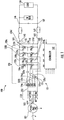
FIG. 1 depicts a block diagram of an electric power generating system with interleaved boost converter and voltage ripple compensation in accordance with one or more embodiments of the present disclosure; -
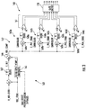
FIG. 2 depicts a simplified control diagram a voltage regulation function for the electric power generation system in accordance with one or more embodiments of the present disclosure; -
FIG. 3 depicts a simplified control diagram a voltage ripple compensation function on for the electric power generation system in accordance with one or more embodiments of the present disclosure; -
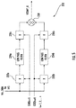
FIG. 4 depicts a simplified control diagram a voltage ripple harmonic compensation function of the voltage ripple compensation function for the electric power generating system in accordance with one or more embodiments of the present disclosure; and -
FIG. 5 depicts a simplified control diagram a voltage ripple harmonic selector of the voltage ripple compensation function for the electric power generating system in accordance with one or more embodiments of the present disclosure; and -
FIG. 6 depicts a method of voltage ripple compensation in a DC power generating system in accordance with one or more embodiments of the present disclosure. - Embodiments described herein are directed to a system and method DC power generating system for a high voltage DC bus, with example embodiments being discussed below in detail. According to example embodiments, technical benefits and improvements in voltage ripple compensation through active control and compensation. In addition, the voltage ripple compensation of the described embodiments reduces requirements with regard to the size of a DC link capacitor and filtering within the DC power generating system, resulting in improved weight, size and cost for the system.
- A detailed description of one or more embodiments of the disclosed apparatus and method are presented herein by way of exemplification and not limitation with reference to the Figures. As shown and described herein, various features of the disclosure will be presented. Various embodiments may have the same or similar features and thus the same or similar features may be labeled with the same reference numeral, but preceded by a different first number indicating the figure to which the feature is shown. Thus, for example, element "a" that is shown in FIG. X may be labeled "Xa" and a similar feature in FIG. Z may be labeled "Za." Although similar reference numbers may be used in a generic sense, various embodiments will be described and various features may include changes, alterations, modifications, etc. as will be appreciated by those of skill in the art, whether explicitly described or otherwise would be appreciated by those of skill in the art.
- The terminology used herein is for the purpose of describing particular embodiments only and is not intended to be limiting of the present disclosure. As used herein, the singular forms "a", "an" and "the" are intended to include the plural forms as well, unless the context clearly indicates otherwise. The term "about" is intended to include the degree of error associated with measurement of the particular quantity based upon the equipment available at the time of filing the application. It will be further understood that the terms "comprises" and/or "comprising," when used in this specification, specify the presence of stated features, integers, steps, operations, elements, and/or components, but do not preclude the presence or addition of one or more other features, integers, steps, operations, element components, and/or groups thereof.
- Turning to
FIG. 1 , a DC power system is shown. TheDC power system 100 may be a power system of a vehicle, for example, a car, truck, or other ground vehicle, aircraft, and the like. As illustrated, thesystem 100 includes a variable speed three-phase permanent magnet generator (PMG) 101. ThePMG 101 is mechanically driven by a prime mover (not shown) and generates a three-phase alternating current (AC) output as is conventionally known. Thesystem 100 may include a voltage sensor(s) 102 in communication with each phase output of thePMG 101. Thevoltage sensor 102 is configured to provide voltage feedback signals for each phase output of thePMG 101 for the purpose of determining PMG electrical angle. In an embodiment the PMG electrical angle may be determined by a Hall-effect sensor that is operably connected to and configured to communicate with a system controller as described herein. - The
system 100 further includes aconventional rectifier 110 in electrical communication withPMG 101. Therectifier 110 includes a plurality of diodes denoted as D1, D2, D3, D4, D5, and D6 to rectify the AC voltages from thePMG 101 to pulse rectifiedDC voltage 112. It will be appreciated that while therectifier 110 is depicted and employs conventional diodes D1-D6, other configurations are possible, including, but not limited to active rectification, employing active switching devices and the like. - The
system 100 further includes a multi-leg interleaved DC-DC boost converter 120. The each leg 122 (depicted as 122a-122d) of theboost converter 120 comprises a series boost inductor 124 (depicted as 124a-124d) operably connected to the mid-point of two series connected switching devices 126, 127 (depicted as 126a-126d and 127a-127d respectively). The current from the pulse rectifiedDC voltage 112 of thePMG 101 is passed to theboost inductor 124a-124d of each leg 122a-122d of theboost converter 120 through the inductances 124 to eachleg 122. The switching devices 126 and 127 are each responsive to a pulse-width modulated (PWM) signals configured to synchronously rectify and convert the pulse rectifiedvoltages 112 from thePMG 101 to DC voltages to supply a DC bus 140. In accordance with an embodiment, the pulse-width modulated signal of each phase of the DC-DC boost converter is phase shifted (interleaved) by 360deg/n, where n is a number of phases of DC-DC boost converter. The interleaving reduces ripple current being directed to the load at the PWM switching frequency. In one example, theboost converter 120 converts the rectified three-phase voltage 112 into 270 volts DC output power at a DC bus 140. In another embodiment the DC bus 140 is 28VDC and may also charge a battery and the like. Theboost converter 120 further includes a plurality ofcurrent transducers phase leg 122 of theboost converter 120. Thecurrent transducers devices 126a-126d and 127a-127d respectively. - In an embodiment the DC bus 140 includes a
positive terminal 142 and anegative terminal 143. The DC bus 140 may also include one or moreDC bus capacitors 144 connecting the positive andnegative terminals voltage sensor 145 coupled in parallel across theDC capacitor 144. Thevoltage sensor 145 is configured to provide voltage feedback for theboost converter 120. Theboost converter 120, and DC bus 140 may further include filter inductors denoted LF1 and LD1 arranged serially from thefirst terminal 142 to afirst output terminal 146 of the DC bus 140, and inductors LF2 and LD2 arranged serially from thesecond terminal 143 to asecond output terminal 147 of the DC bus 140. In an embodiment, resistors RD1 and RD2 may further be arranged in parallel communication with inductances LD1 and LD2, respectively. Furthermore, a filter capacitor CF may be arranged across thefirst output terminal 146 andsecond output terminal 147 of the DC 140 bus. The filter inductors LF1, LD1, LF2, LD2, resistors RD1 and RD2 operably cooperate with filter capacitor CF to provide further voltage ripple and EMI reduction at the output of the DC voltage bus 140. Additional EMI filtering may also optionally be employed as depicted in the figure. - The
system 100 further includesload 150 in communication with theoutput terminals 146/147 of DC bus 140. Theload 150 may be any suitable DC load applied to theoutput DC bus 146/147. For example, as described above, theDC load 150 may be constant power DC load. - Turning now to
FIG. 2 andFIG. 3 as well.FIG 2 depicts a simplified block diagram of the functions and interfaces of thecontroller 160.FIG. 3 depicts additional function detail of the functions of thecontroller 160. Thesystem 100 optionally includes the gate drives 170 in communication with theswitching devices 126a-d and 127a-d of theboost converter 120. The gate drives 170 may be configured to open and close each of the plurality of switchingdevices 126a-d and 127a-d in accordance with a selected gate control scheme to cause theboost converter 120 to synchronously rectify and convert the pulse rectifiedvoltages 112 to generate the DC voltages of DC bus 140. Thesystem 100 further includescontroller 160 in communication with the gate drives 170 and/or theswitching devices 126a-d and 127a-d and applies a pulse width modulated (PWM) signal to the gate drives 170 or switchingdevices 126a-d and 127a-d to implement the conversion. - In an embodiment the
controller 160 further includes various processes and function configured to implement the functionality of theboost converter 120. In an embodiment thecontroller 160 includes aPWM modulator function 161 configured to provide the PWM signal(s). The outputs ofPWM function 161 are connected to the MOSFET gates of theswitching devices 126a-126d and 127a-127d respectively viagate drive 170. In operation, thecontroller 160 also includes acurrent regulation function 162 that operates in communication with aPWM function 161 to generate the PWM signals that control the gate drives 170 or switchingdevices 126a-d and 127a-d in response to the voltage regulator output signal I_ref_comp. For example, thecurrent regulator function 162 may be in in operable communication with the plurality ofcurrent transducers 121a-121d to control the function of theboost converter 120 and supply the DC bus 140 and ultimately theload 150. In an embodiment thecurrent regulator 162 includes a plurality of current regulators denoted 162a-162d, one for each of the legs 122a-122d of theboost converter 120. - In an embodiment the each
regulator function 162a-162d includes a summer 169a-169d for eachcurrent regulator 162a-162d to receive a compensated current reference denoted as I ref comp and each feedback current as sensed by thecurrent transducers 121a-121d. A current error signal is then directed to a proportional integral (PI) controller denoted 168a-168d respectively for eachcurrent regulator 162a-162d (FIG. 3 ) employed to monitor the voltage of the DC bus 140 and generate a reference command for thecurrent regulator function 162. - The
controller 160 further includesvoltage regulator function 163 in communication with thecurrent regulator function 162. For example, thevoltage regulator function 163 of thecontroller 160 may be in operable communication with thevoltage sensor 145 of theboost converter 120 and more specifically the DC bus 140. Thevoltage regulator function 166 monitors thesensor 145 and provides a current reference to control the synchronouscurrent regulator function 162, and there by the boost converter 120 (via theswitching devices 126a-d and 127a-d to maintain the voltage on the DC bus 140 at a prescribed level. In an embodiment thevoltage regulator function 163 includes a proportional integral (PI) controller 167 (FIG. 3 ) employed to monitor the voltage of the DC bus 140 and generate a reference command for thecurrent regulator function 162. - The
controller 160 further includes PMG electricalangle estimator function 164 in communication with thevoltage regulator function 163, thecurrent regulator function 162, and thevoltage sensor 145. The PMG electricalangle estimator function 164 may be configured to estimate an electrical angle ofPMG 101, and provide the estimation tocurrent regulator 162. Furthermore, the PMGelectrical angle estimator 164 may be configured to estimate a rotational speed of thePMG 101 and provide the speed estimation to thevoltage regulator function 163 as is known in the art. - Continuing with
FIG. 2 , and turning now toFIG. 3 as well, where further detail of the functions of thecontroller 160 are depicted. Thevoltage regulator function 163 of thecontroller 160 also includes a voltageripple compensator function 165. Thevoltage ripple compensator 165 provides compensation to the current reference established in thevoltage regulator 163 as described in further detail herein. For example, in an embodiment, the output of the voltageripple compensator function 165 is added atsummer 166 to the output ofPI controller 167 in thevoltage regulator function 163 to form a modulated current reference applied to current regulator(s) 162. In an embodiment, the set ofcurrent regulators 162, that is, one current regulator denoted as 162a - 162d is employed to control each phase leg 122a-122d respectively. In operation, thePI controllers 168a-168d provides control inputs to cause thecurrent regulators 162a-162d to control the voltage on the DC bus 140. Furthermore, thevoltage compensation function 165 provides compensation inputs to thecurrent regulators 162a-162d to cancel or reduce voltage ripple on the DC bus 140 as will be described in further detail herein. Furthermore, the carrier signal of each of the current regulator pulse-width-modulator (PWM) is phase shifted in relationship with the next one (interleaving). In an embodiment the phase shifting is based on the number oflegs 122 employed in theboost converter 120. That is, to facilitate the interleaving the control of the current regulator(s) are phase shifted by 360/n where n is the number ofphase legs 122 employed in theboost converter 120. In an embodiment employing four phase legs 122a-122d as described, the PWM carrier for each phase leg 122a-122d is shifted by 90 degrees respectively. -
FIG 4 depicts a further detailed diagram of a voltageripple compensation function 165 also denoted as 200. In an embodiment, the voltageripple compensation function harmonic selectors 230. ThePLL 210 facilitates synchronization with the ripple generated by the rectification of the PMG voltages. ThePLL 210 receives rotor position signals for the threephase PMG 101 derive the rotary position of thePMG 101. The rotary position is then converted to anelectrical angle 211 by multiplying by the number of pole-pairs in thePMG 101 as depicted in thePLL 210. Theelectrical angle 211 for thePMG 101 is then multiplied by six atmultiplier 212. Multiplication by six facilitates identification and selection of the voltage ripple that is equal 6-times of fundamental PMG frequency (as generated by the 6-pulse rectifier 110). The derived signal 213 is multiplied a number (k=1, 2..n) at multiplier 214 (referenced specifically as 214a-214n) corresponding to the harmonic (e.g., fundamental, 2nd, 3rd etc.) of the voltage ripple on the voltage of the DC bus 140 to be compensated or reduced. The direct and quadrature vector components of the input vector (signal Vdc_fdbk) are formulated in a quadrature generator [sin(kωt) and cos(kωt)] 240a-240n by utilizing sin and cos functions. - Turning now to
FIG. 5 , where a further detailed representation of the voltage rippleharmonic selector 230 is depicted. In an embodiment, the DC bus voltage signal (Vdc_fdbk) as measured bysensor 145 is applied to input of voltage rippleharmonic selectors 230 denoted 230a-230n. The quadrature signals (sin(kωt) and cos(kωt)) corresponding to a particular harmonic k are applied to a particular voltage rippleharmonic selector 230a-230n respectively. The direct and quadrature vector components e.g., (corresponding to sin and cos) of the input vector (signal Vdc_fdbk) of the quadrature generator [sin(kωt) and cos(kωt)] for the selected frequency are selected as dc quantities at the outputs of first multipliers denoted 232a and 232b. The high frequency components are filtered out bylow pass filters multipliers multipliers summer 238. The resulting time-varying signal formed at thesummer output 238 and has amplitude, frequency, and phase of the selected harmonic of the dc link voltage ripple. The output of each particular voltage rippleharmonic selector 230a-230n produces a compensation signal (denoted Vcomp_1-Vcomp_n) associated with each harmonic k selected for compensation. Each of the compensation signals Vcomp_1-Vcomp_n is added at the output summer 250 (FIG. 4 ) to formulate a voltage ripple compensation signal as discussed with respect toFIG. 3 . -
FIG. 6 depicts amethod 600 of reducing voltage ripple in a DCpower generation system 100 in accordance with one or more embodiments of the present disclosure. Themethod 600 includes operably connecting apassive rectifier 110 to thePMG 101 as depicted atprocess step 610. Atprocess step 620, themethod 600 continues with operably connecting aboost converter 120 to thepassive rectifier 110. Acontroller 160 is operably connected in electrical communication with thePMG 101 and theboost converter 120 as depicted atprocess step 630. Thecontroller 160 is configured to execute a process to cause theboost converter 120 to supply a DC bus 140 based on a voltage compensation signal to theboost converter 120 to reduce voltage ripple on the voltage of the DC bus 140 as depicted atprocess step 640. - The
method 600 may also include thecontroller 160 including a current regulator function 162 (FIG. 2 ), where thecurrent regulator function 162 is configured to provide a pulse width modulation (PWM) scheme to theboost converter 120 based on quadrature components of feedback voltage harmonics of theboost converter 120. Furthermore, themethod 600 includes avoltage regulator function 163 in communication with thecurrent regulator function 162, wherein thevoltage regulator function 163 is configured to provide a compensated reference current to thecurrent regulator 162. Themethod 600 may also include an electricalangle estimator function 164, the electricalangle estimator function 164 is configured to estimate the electrical angle of power generated at thePMG 101. The electricalangle estimator function 164 also communicates with thevoltage regulator function 163, which provides quadrature components of a feedback voltage output harmonics as sensed bysensor 145 to thecurrent regulator 162, the quadrature components of the feedback voltage output harmonics being based on the estimated electrical angle of thePMG 101 and the feedback voltage. - The present embodiments may be a system, a method, and/or a computer program product at any possible technical detail level of integration. The computer program product may include a computer readable storage medium (or media) having computer readable program instructions thereon for causing a processor to carry out aspects of the present disclosure.
- The computer readable storage medium can be a tangible device that can retain and store instructions for use by an instruction execution device. The computer readable storage medium may be, for example, but is not limited to, an electronic storage device, a magnetic storage device, an optical storage device, an electromagnetic storage device, a semiconductor storage device, or any suitable combination of the foregoing. A non-exhaustive list of more specific examples of the computer readable storage medium includes the following: a portable computer diskette, a hard disk, a random access memory (RAM), a read-only memory (ROM), an erasable programmable read-only memory (EPROM or Flash memory), a static random access memory (SRAM), a portable compact disc read-only memory (CD-ROM), a digital versatile disk (DVD), a memory stick, a floppy disk, a mechanically encoded device such as punch-cards or raised structures in a groove having instructions recorded thereon, and any suitable combination of the foregoing. A computer readable storage medium, as used herein, is not to be construed as being transitory signals per se, such as radio waves or other freely propagating electromagnetic waves, electromagnetic waves propagating through a waveguide or other transmission media (e.g., light pulses passing through a fiber-optic cable), or electrical signals transmitted through a wire.
- Computer readable program instructions described herein can be downloaded to respective computing/processing devices from a computer readable storage medium or to an external computer or external storage device via a network, for example, the Internet, a local area network, a wide area network and/or a wireless network. The network may comprise copper transmission cables, optical transmission fibers, wireless transmission, routers, firewalls, switches, gateway computers and/or edge servers. A network adapter card or network interface in each computing/processing device receives computer readable program instructions from the network and forwards the computer readable program instructions for storage in a computer readable storage medium within the respective computing/processing device.
- Aspects of the present invention are described herein with reference to flowchart illustrations and/or block diagrams of methods, apparatus (systems), and computer program products according to embodiments. It will be understood that each block of the flowchart illustrations and/or block diagrams, and combinations of blocks in the flowchart illustrations and/or block diagrams, can be implemented by computer readable program instructions. The flowchart and block diagrams in the Figures illustrate the architecture, functionality, and operation of possible implementations of systems, methods, and computer program products according to various embodiments. In this regard, each block in the flowchart or block diagrams may represent a module, segment, or portion of instructions, which comprises one or more executable instructions for implementing the specified logical function(s). In some alternative implementations, the functions noted in the blocks may occur out of the order noted in the Figures. For example, two blocks shown in succession may, in fact, be executed substantially concurrently, or the blocks may sometimes be executed in the reverse order, depending upon the functionality involved. It will also be noted that each block of the block diagrams and/or flowchart illustration, and combinations of blocks in the block diagrams and/or flowchart illustration, can be implemented by special purpose hardware-based systems that perform the specified functions or acts or carry out combinations of special purpose hardware and computer instructions.
- While the present disclosure has been described with reference to an exemplary embodiment or embodiments, it will be understood by those skilled in the art that various changes may be made without departing from the scope of the invention as defined by the claims. In addition, many modifications may be made to adapt a particular situation or material to the teachings of the present disclosure without departing from the scope of the invention. Therefore, it is intended that the present disclosure not be limited to the particular embodiment disclosed as the best mode contemplated for carrying out this present disclosure, but that the present disclosure will include all embodiments falling within the scope of the claims.
Claims (15)
- A system for providing voltage ripple compensation in a DC power generation system, the system comprising:a permanent magnet generator, PMG (101);a passive rectifier (110) in operable communication with the PMG;a multi-phase interleaved DC-DC boost converter (120) in operable communication with the passive rectifier; anda controller (160) in electrical communication with the boost converter, wherein the controller is configured to cause the boost converter to supply a DC bus (140) and wherein the controller is configured to control the boost converter based on desired DC bus voltage and on a voltage compensation signal to the boost converter to reduce voltage ripple on the voltage of the DC bus, wherein the voltage compensation signal is based at least in part on d-q components of harmonics of a DC bus feedback voltage due to 6-pulse passive rectification;wherein the controller includes a current regulator (162) in electrical communication with the boost converter, and wherein the current regulator is configured to provide a current regulation scheme to the boost converter based on desired DC bus voltage, the voltage compensation signal and at least one feedback current of the boost converter,wherein the controller further includes a voltage regulator (163) in communication with the current regulator, wherein the voltage regulator is configured to provide a compensated reference current to the current regulator,wherein the controller further includes an electrical angle estimator (164) in communication with the PMG and the current regulator, andwherein the voltage regulator is in communication with the electrical angle estimator, and wherein the voltage regulator is configured to provide quadrature components of the harmonics of the DC bus feedback voltage at the boost converter to the current regulator, the quadrature components of the feedback voltage output harmonics being based on the estimated electrical angle of the PMG and the feedback voltage.
- The system of claim 1, wherein the controller further includes a pulse width modulation, PWM, modulator (161) in communication with the current regulator and the boost converter, the PWM modulator configured to control the boost converter based on a compensated reference current and a current of the boost converter.
- The system of claim 1 or 2, wherein the current regulator is configured to provide a current regulation scheme to the boost converter through regulation of the boost converter current.
- The system of claim 1 or 2, wherein the current regulator is configured provide to a current regulation scheme to the boost converter based on proportional - integral of current errors of the of the boost converter.
- The system of any preceding claim, wherein the voltage regulator comprises a phase locked loop configured to generate an electrical angle of the PMG based on a position sensor associated with the PMG and a number of pole-pairs in the PMG.
- The system of any preceding claim, wherein the voltage regulator comprises a harmonic selector configured to select a harmonic or a plurality of harmonics on DC bus after passive rectification of the PMG output to be compensated.
- The system of any of claims 1 to 5, wherein the voltage regulator comprises a voltage ripple harmonic selector (230), the voltage ripple harmonic selector configured to select a harmonic of a plurality of harmonics associated with the DC bus voltage generated by the passive rectification of the PMG output and generate a compensation signal based on the PMG electrical angle and the voltage of the DC bus.
- The system of claim 7, wherein the voltage ripple compensation signal is a summation of voltage compensation signals for each harmonic of a plurality of harmonics selected.
- The system of any preceding claim, wherein the PMG is a three phase generator and the passive rectifier is a six-pulse rectifier.
- A method for providing voltage ripple compensation in a DC power generation system having a permanent magnet generator, PMG, the method including:operably connecting a passive rectifier to the PMG;operably connecting a multi-phase interleaved DC-DC boost converter to the passive rectifier;operably connecting a controller in electrical communication with the PMG and boost converter, wherein the controller is configured to execute a process to cause the boost converter to supply a desired DC bus output voltage and wherein the controller is configured to control the boost converter based on the desired DC bus output voltage and a voltage compensation signal to the boost converter to reduce voltage ripple on the voltage of the DC bus, wherein the voltage compensation signal is based at least in part on d-q components of harmonics of a feedback voltage harmonics on the DC bus caused by passive rectification of PMG output;causing the the controller to executing a current regulator function, and wherein the current regulator is configured to provide a current regulation scheme to the boost converter based on the voltage compensation signal and at least one feedback current of the boost converter,wherein the controller further includes a voltage regulator function in communication with the current regulator function, wherein the voltage regulator function is configured to provide a compensated reference current to the current regulator,wherein the controller further includes an electrical angle estimator function, the electrical angle estimator function configured to estimate at least an angle of power generated at the PMG, andwherein the voltage regulator function communicates with the electrical angle estimator function, and the voltage regulator function provides the quadrature components of the harmonics of the feedback voltage at the boost converter to the current regulator, the quadrature components of the harmonics of the feedback voltage being based on the estimated electrical angle of the PMG and the feedback voltage.
- The method of claim 10, further including a pulse width modulation (PWM) modulator function in communication with the current regulator and the boost converter, the PWM modulator function configured to control the boost converter based on a compensated reference current and a current of the boost converter.
- The method of claim 10, further including configuring the current regulator function to provide a current regulation scheme to the boost converter through regulation of the boost converter current.
- The method of claim 10, further including configuring the current regulator function to provide a current regulation scheme to the boost converter based on proportional - integral of current errors of the of the boost converter.
- The method of claim 10, wherein the voltage regulator function comprises a phase locked loop configured to generate an electrical angle of the PMG based on a position sensor associated with the PMG and a number of pole-pairs in the PMG.
- The method of claim 14, wherein the voltage regulator function comprises a harmonic selector configured to select a harmonic of a plurality of harmonics of a voltage generated by the PMG after passive rectification to be compensated.
Applications Claiming Priority (1)
| Application Number | Priority Date | Filing Date | Title |
|---|---|---|---|
| US16/054,689 US10541598B1 (en) | 2018-08-03 | 2018-08-03 | DC power generating system with voltage ripple compensation |
Publications (2)
| Publication Number | Publication Date |
|---|---|
| EP3605812A1 true EP3605812A1 (en) | 2020-02-05 |
| EP3605812B1 EP3605812B1 (en) | 2021-03-17 |
Family
ID=67539300
Family Applications (1)
| Application Number | Title | Priority Date | Filing Date |
|---|---|---|---|
| EP19189668.7A Active EP3605812B1 (en) | 2018-08-03 | 2019-08-01 | Dc power generating system with voltage ripple compensation |
Country Status (2)
| Country | Link |
|---|---|
| US (1) | US10541598B1 (en) |
| EP (1) | EP3605812B1 (en) |
Cited By (1)
| Publication number | Priority date | Publication date | Assignee | Title |
|---|---|---|---|---|
| GB2577975A (en) * | 2018-08-13 | 2020-04-15 | Hamilton Sundstrand Corp | Electric system architecture with a permanent magnet generator and interleaved active rectifiers |
Families Citing this family (12)
| Publication number | Priority date | Publication date | Assignee | Title |
|---|---|---|---|---|
| US20200127455A1 (en) * | 2018-10-21 | 2020-04-23 | Technology Innovation Momentum Fund (Israel) Limited Partnership | Device and Method for Controlling DC Bus Ripple |
| US10855166B2 (en) * | 2019-03-11 | 2020-12-01 | Infineon Technologies Ag | Ripple shaping for switch-mode power supply using number of active phases |
| FR3103228B1 (en) * | 2019-11-15 | 2021-10-29 | Valeo Equip Electr Moteur | ENGINE MODE END OF CONTROL MODULE AND MANAGEMENT PROCESS FOR A ROTATING ELECTRIC MACHINE |
| CN111262425B (en) * | 2020-03-31 | 2021-03-09 | 安可达技术(苏州)有限公司 | Control system and method of staggered totem-pole power factor correction circuit |
| US12176821B2 (en) * | 2021-05-13 | 2024-12-24 | Vertiv Corporation | Intelligent rectifier current regulation of DC bus voltage droop |
| CN113341226B (en) * | 2021-06-21 | 2022-04-29 | 合肥美的暖通设备有限公司 | Harmonic detection method, device, frequency converter and storage medium |
| US12015353B1 (en) * | 2021-07-12 | 2024-06-18 | Smart Wires Inc. | Attenuating harmonic current in power transmission lines |
| US11533013B1 (en) * | 2021-07-29 | 2022-12-20 | Rivian Ip Holdings, Llc | Pulse width modulation clock synchronization |
| EP4160891A1 (en) | 2021-10-04 | 2023-04-05 | Hamilton Sundstrand Corporation | Active rectifier harmonics compensator |
| US11855544B2 (en) * | 2022-02-03 | 2023-12-26 | Lee Fredrik Mazurek | Single stage synchronous harmonic current controlled power system |
| JP7464925B2 (en) * | 2022-02-28 | 2024-04-10 | 矢崎総業株式会社 | Charger |
| US11855545B1 (en) * | 2023-09-10 | 2023-12-26 | Lee Fredrik Mazurek | Single stage synchronous generalized regulator |
Citations (1)
| Publication number | Priority date | Publication date | Assignee | Title |
|---|---|---|---|---|
| US20150145325A1 (en) * | 2012-06-22 | 2015-05-28 | Eaton Corporation | Active power factor correction for aircraft power system harmonic mitigation |
Family Cites Families (18)
| Publication number | Priority date | Publication date | Assignee | Title |
|---|---|---|---|---|
| US5140245A (en) * | 1990-09-24 | 1992-08-18 | Westinghouse Electric Corp. | Pmg-based position sensor and synchronous drive incorporating same |
| US5218520A (en) | 1991-11-27 | 1993-06-08 | Rozman Gregory I | Vscf system with reduced dc link ripple |
| US6545887B2 (en) * | 1999-08-06 | 2003-04-08 | The Regents Of The University Of California | Unified constant-frequency integration control of three-phase power factor corrected rectifiers, active power filters and grid-connected inverters |
| ATE442693T1 (en) * | 2000-01-28 | 2009-09-15 | Cummins Generator Technologies | AC GENERATION SYSTEM |
| US6850426B2 (en) * | 2002-04-30 | 2005-02-01 | Honeywell International Inc. | Synchronous and bi-directional variable frequency power conversion systems |
| US7224147B2 (en) | 2005-07-20 | 2007-05-29 | Hamilton Sundstrand Corporation | Buck/boost method of voltage regulation for a permanent magnet generator (PMG) |
| US7859230B2 (en) | 2007-12-26 | 2010-12-28 | Pratt & Whitney Canada Corp | Voltage regulation to reduce ripple in a power generation system |
| CN102460338B (en) * | 2009-05-19 | 2014-08-13 | 最大输出可再生能源公司 | Construction of a power station comprising a cluster of power generating units |
| US8378641B2 (en) | 2010-07-12 | 2013-02-19 | Hamilton Sundstrand Corporation | Electric power generating system with boost converter/synchronous active filter |
| WO2012049706A1 (en) * | 2010-10-13 | 2012-04-19 | 三菱電機株式会社 | Three-phase ac/dc converting apparatus and air handling unit using three-phase ac/dc converting apparatus |
| US9059647B2 (en) | 2010-11-16 | 2015-06-16 | Hamilton Sundstrand Corporation | High voltage DC power generation |
| US20120126758A1 (en) | 2010-11-19 | 2012-05-24 | Hamilton Sundstrand Corporation | High voltage dc power generation |
| KR101288638B1 (en) | 2011-12-27 | 2013-07-22 | 주식회사 효성 | Current ripple reduction device for double fed induction wind generator and method therefore |
| US20130181654A1 (en) * | 2012-01-18 | 2013-07-18 | Hamilton Sundstrand Corporation | Motor drive system employing an active rectifier |
| US9602025B2 (en) * | 2013-07-12 | 2017-03-21 | Infineon Technologies Austria Ag | Multiphase power converter circuit and method |
| JP5997677B2 (en) * | 2013-10-16 | 2016-09-28 | ダイキン工業株式会社 | Power converter and air conditioner |
| KR102314037B1 (en) * | 2014-06-09 | 2021-10-15 | 엘지전자 주식회사 | Mootor driver and air conditioner including the same |
| US11043880B2 (en) | 2016-11-10 | 2021-06-22 | Hamilton Sunstrand Corporation | Electric power generating system with a synchronous generator |
-
2018
- 2018-08-03 US US16/054,689 patent/US10541598B1/en active Active
-
2019
- 2019-08-01 EP EP19189668.7A patent/EP3605812B1/en active Active
Patent Citations (1)
| Publication number | Priority date | Publication date | Assignee | Title |
|---|---|---|---|---|
| US20150145325A1 (en) * | 2012-06-22 | 2015-05-28 | Eaton Corporation | Active power factor correction for aircraft power system harmonic mitigation |
Cited By (2)
| Publication number | Priority date | Publication date | Assignee | Title |
|---|---|---|---|---|
| GB2577975A (en) * | 2018-08-13 | 2020-04-15 | Hamilton Sundstrand Corp | Electric system architecture with a permanent magnet generator and interleaved active rectifiers |
| GB2577975B (en) * | 2018-08-13 | 2022-08-03 | Hamilton Sundstrand Corp | Electric system architecture with a permanent magnet generator and interleaved active rectifiers |
Also Published As
| Publication number | Publication date |
|---|---|
| US10541598B1 (en) | 2020-01-21 |
| US20200044558A1 (en) | 2020-02-06 |
| EP3605812B1 (en) | 2021-03-17 |
Similar Documents
| Publication | Publication Date | Title |
|---|---|---|
| EP3605812B1 (en) | Dc power generating system with voltage ripple compensation | |
| CA2726056C (en) | Method and system for reducing switching losses in a high-frequency multi-cell power supply | |
| US8471514B2 (en) | Adaptive harmonic reduction apparatus and methods | |
| CN112542955B (en) | Power conversion system, controller, and computer readable medium | |
| JP6503277B2 (en) | Controller and AC motor drive | |
| CA2719584A1 (en) | Dc bus voltage harmonics reduction | |
| EP1921740A2 (en) | Power converter control | |
| US20130181654A1 (en) | Motor drive system employing an active rectifier | |
| US10135352B2 (en) | Controller for power converter with frequency modulated carrier | |
| US10651770B2 (en) | Direct current voltage regulation of a six-phase permanent magnet generator | |
| EP2779403A1 (en) | Power conversion system and method | |
| EP3082246A1 (en) | Systems and methods for controlling inverters | |
| EP3010143B1 (en) | Method for controlling force ripples of a generator | |
| Alnajjar et al. | Predictive control of variable frequency brushless excited synchronous generator for more electric aircraft power system | |
| Verkroost et al. | Module connection topologies and interleaving strategies for integrated modular motor drives | |
| Gandomi et al. | A fault tolerant T-type inverter for five-phase PMSM drives | |
| JP2010220332A (en) | Power converting device | |
| Pontt et al. | Output sinus filter for medium voltage drive with direct torque control | |
| Kabalci et al. | Comparison of model predictive torque control based NPC and ANPC inverters for IM drive | |
| Bahrami-Fard et al. | An Effective Current Harmonic Suppression Strategy for Three-Phase Vienna Rectifiers | |
| Neve et al. | Analysis and simulation of Z-source inverter fed to single phase induction motor drive | |
| Koiwa et al. | Efficiency evaluation of a matrix converter with a boost-up AC chopper in an adjustable drive system | |
| US10547259B1 (en) | Electric generating system with an interleaved DC-DC converter | |
| Guzman et al. | Predictive control of modular current source converters | |
| Mariem et al. | Active Filtering and Power Factor Correction for Electric Vehicles |
Legal Events
| Date | Code | Title | Description |
|---|---|---|---|
| PUAI | Public reference made under article 153(3) epc to a published international application that has entered the european phase |
Free format text: ORIGINAL CODE: 0009012 |
|
| STAA | Information on the status of an ep patent application or granted ep patent |
Free format text: STATUS: THE APPLICATION HAS BEEN PUBLISHED |
|
| AK | Designated contracting states |
Kind code of ref document: A1 Designated state(s): AL AT BE BG CH CY CZ DE DK EE ES FI FR GB GR HR HU IE IS IT LI LT LU LV MC MK MT NL NO PL PT RO RS SE SI SK SM TR |
|
| AX | Request for extension of the european patent |
Extension state: BA ME |
|
| STAA | Information on the status of an ep patent application or granted ep patent |
Free format text: STATUS: REQUEST FOR EXAMINATION WAS MADE |
|
| 17P | Request for examination filed |
Effective date: 20200805 |
|
| RBV | Designated contracting states (corrected) |
Designated state(s): AL AT BE BG CH CY CZ DE DK EE ES FI FR GB GR HR HU IE IS IT LI LT LU LV MC MK MT NL NO PL PT RO RS SE SI SK SM TR |
|
| GRAP | Despatch of communication of intention to grant a patent |
Free format text: ORIGINAL CODE: EPIDOSNIGR1 |
|
| STAA | Information on the status of an ep patent application or granted ep patent |
Free format text: STATUS: GRANT OF PATENT IS INTENDED |
|
| RIC1 | Information provided on ipc code assigned before grant |
Ipc: H02M 7/06 20060101ALI20200925BHEP Ipc: H02M 1/15 20060101AFI20200925BHEP Ipc: H02M 1/00 20060101ALI20200925BHEP Ipc: H02M 3/158 20060101ALI20200925BHEP Ipc: H02P 9/00 20060101ALI20200925BHEP |
|
| INTG | Intention to grant announced |
Effective date: 20201016 |
|
| GRAS | Grant fee paid |
Free format text: ORIGINAL CODE: EPIDOSNIGR3 |
|
| GRAA | (expected) grant |
Free format text: ORIGINAL CODE: 0009210 |
|
| STAA | Information on the status of an ep patent application or granted ep patent |
Free format text: STATUS: THE PATENT HAS BEEN GRANTED |
|
| AK | Designated contracting states |
Kind code of ref document: B1 Designated state(s): AL AT BE BG CH CY CZ DE DK EE ES FI FR GB GR HR HU IE IS IT LI LT LU LV MC MK MT NL NO PL PT RO RS SE SI SK SM TR |
|
| REG | Reference to a national code |
Ref country code: GB Ref legal event code: FG4D |
|
| REG | Reference to a national code |
Ref country code: CH Ref legal event code: EP |
|
| REG | Reference to a national code |
Ref country code: DE Ref legal event code: R096 Ref document number: 602019003230 Country of ref document: DE |
|
| REG | Reference to a national code |
Ref country code: IE Ref legal event code: FG4D |
|
| REG | Reference to a national code |
Ref country code: AT Ref legal event code: REF Ref document number: 1373170 Country of ref document: AT Kind code of ref document: T Effective date: 20210415 |
|
| REG | Reference to a national code |
Ref country code: LT Ref legal event code: MG9D |
|
| PG25 | Lapsed in a contracting state [announced via postgrant information from national office to epo] |
Ref country code: HR Free format text: LAPSE BECAUSE OF FAILURE TO SUBMIT A TRANSLATION OF THE DESCRIPTION OR TO PAY THE FEE WITHIN THE PRESCRIBED TIME-LIMIT Effective date: 20210317 Ref country code: BG Free format text: LAPSE BECAUSE OF FAILURE TO SUBMIT A TRANSLATION OF THE DESCRIPTION OR TO PAY THE FEE WITHIN THE PRESCRIBED TIME-LIMIT Effective date: 20210617 Ref country code: GR Free format text: LAPSE BECAUSE OF FAILURE TO SUBMIT A TRANSLATION OF THE DESCRIPTION OR TO PAY THE FEE WITHIN THE PRESCRIBED TIME-LIMIT Effective date: 20210618 Ref country code: FI Free format text: LAPSE BECAUSE OF FAILURE TO SUBMIT A TRANSLATION OF THE DESCRIPTION OR TO PAY THE FEE WITHIN THE PRESCRIBED TIME-LIMIT Effective date: 20210317 Ref country code: NO Free format text: LAPSE BECAUSE OF FAILURE TO SUBMIT A TRANSLATION OF THE DESCRIPTION OR TO PAY THE FEE WITHIN THE PRESCRIBED TIME-LIMIT Effective date: 20210617 |
|
| REG | Reference to a national code |
Ref country code: AT Ref legal event code: MK05 Ref document number: 1373170 Country of ref document: AT Kind code of ref document: T Effective date: 20210317 |
|
| REG | Reference to a national code |
Ref country code: NL Ref legal event code: MP Effective date: 20210317 |
|
| PG25 | Lapsed in a contracting state [announced via postgrant information from national office to epo] |
Ref country code: RS Free format text: LAPSE BECAUSE OF FAILURE TO SUBMIT A TRANSLATION OF THE DESCRIPTION OR TO PAY THE FEE WITHIN THE PRESCRIBED TIME-LIMIT Effective date: 20210317 Ref country code: SE Free format text: LAPSE BECAUSE OF FAILURE TO SUBMIT A TRANSLATION OF THE DESCRIPTION OR TO PAY THE FEE WITHIN THE PRESCRIBED TIME-LIMIT Effective date: 20210317 Ref country code: LV Free format text: LAPSE BECAUSE OF FAILURE TO SUBMIT A TRANSLATION OF THE DESCRIPTION OR TO PAY THE FEE WITHIN THE PRESCRIBED TIME-LIMIT Effective date: 20210317 |
|
| PG25 | Lapsed in a contracting state [announced via postgrant information from national office to epo] |
Ref country code: NL Free format text: LAPSE BECAUSE OF FAILURE TO SUBMIT A TRANSLATION OF THE DESCRIPTION OR TO PAY THE FEE WITHIN THE PRESCRIBED TIME-LIMIT Effective date: 20210317 |
|
| PG25 | Lapsed in a contracting state [announced via postgrant information from national office to epo] |
Ref country code: LT Free format text: LAPSE BECAUSE OF FAILURE TO SUBMIT A TRANSLATION OF THE DESCRIPTION OR TO PAY THE FEE WITHIN THE PRESCRIBED TIME-LIMIT Effective date: 20210317 Ref country code: EE Free format text: LAPSE BECAUSE OF FAILURE TO SUBMIT A TRANSLATION OF THE DESCRIPTION OR TO PAY THE FEE WITHIN THE PRESCRIBED TIME-LIMIT Effective date: 20210317 Ref country code: CZ Free format text: LAPSE BECAUSE OF FAILURE TO SUBMIT A TRANSLATION OF THE DESCRIPTION OR TO PAY THE FEE WITHIN THE PRESCRIBED TIME-LIMIT Effective date: 20210317 Ref country code: AT Free format text: LAPSE BECAUSE OF FAILURE TO SUBMIT A TRANSLATION OF THE DESCRIPTION OR TO PAY THE FEE WITHIN THE PRESCRIBED TIME-LIMIT Effective date: 20210317 Ref country code: SM Free format text: LAPSE BECAUSE OF FAILURE TO SUBMIT A TRANSLATION OF THE DESCRIPTION OR TO PAY THE FEE WITHIN THE PRESCRIBED TIME-LIMIT Effective date: 20210317 |
|
| PG25 | Lapsed in a contracting state [announced via postgrant information from national office to epo] |
Ref country code: PL Free format text: LAPSE BECAUSE OF FAILURE TO SUBMIT A TRANSLATION OF THE DESCRIPTION OR TO PAY THE FEE WITHIN THE PRESCRIBED TIME-LIMIT Effective date: 20210317 Ref country code: PT Free format text: LAPSE BECAUSE OF FAILURE TO SUBMIT A TRANSLATION OF THE DESCRIPTION OR TO PAY THE FEE WITHIN THE PRESCRIBED TIME-LIMIT Effective date: 20210719 Ref country code: RO Free format text: LAPSE BECAUSE OF FAILURE TO SUBMIT A TRANSLATION OF THE DESCRIPTION OR TO PAY THE FEE WITHIN THE PRESCRIBED TIME-LIMIT Effective date: 20210317 Ref country code: SK Free format text: LAPSE BECAUSE OF FAILURE TO SUBMIT A TRANSLATION OF THE DESCRIPTION OR TO PAY THE FEE WITHIN THE PRESCRIBED TIME-LIMIT Effective date: 20210317 Ref country code: IS Free format text: LAPSE BECAUSE OF FAILURE TO SUBMIT A TRANSLATION OF THE DESCRIPTION OR TO PAY THE FEE WITHIN THE PRESCRIBED TIME-LIMIT Effective date: 20210717 |
|
| REG | Reference to a national code |
Ref country code: DE Ref legal event code: R097 Ref document number: 602019003230 Country of ref document: DE |
|
| PLBE | No opposition filed within time limit |
Free format text: ORIGINAL CODE: 0009261 |
|
| STAA | Information on the status of an ep patent application or granted ep patent |
Free format text: STATUS: NO OPPOSITION FILED WITHIN TIME LIMIT |
|
| PG25 | Lapsed in a contracting state [announced via postgrant information from national office to epo] |
Ref country code: ES Free format text: LAPSE BECAUSE OF FAILURE TO SUBMIT A TRANSLATION OF THE DESCRIPTION OR TO PAY THE FEE WITHIN THE PRESCRIBED TIME-LIMIT Effective date: 20210317 Ref country code: DK Free format text: LAPSE BECAUSE OF FAILURE TO SUBMIT A TRANSLATION OF THE DESCRIPTION OR TO PAY THE FEE WITHIN THE PRESCRIBED TIME-LIMIT Effective date: 20210317 Ref country code: AL Free format text: LAPSE BECAUSE OF FAILURE TO SUBMIT A TRANSLATION OF THE DESCRIPTION OR TO PAY THE FEE WITHIN THE PRESCRIBED TIME-LIMIT Effective date: 20210317 |
|
| 26N | No opposition filed |
Effective date: 20211220 |
|
| PG25 | Lapsed in a contracting state [announced via postgrant information from national office to epo] |
Ref country code: SI Free format text: LAPSE BECAUSE OF FAILURE TO SUBMIT A TRANSLATION OF THE DESCRIPTION OR TO PAY THE FEE WITHIN THE PRESCRIBED TIME-LIMIT Effective date: 20210317 |
|
| PG25 | Lapsed in a contracting state [announced via postgrant information from national office to epo] |
Ref country code: MC Free format text: LAPSE BECAUSE OF FAILURE TO SUBMIT A TRANSLATION OF THE DESCRIPTION OR TO PAY THE FEE WITHIN THE PRESCRIBED TIME-LIMIT Effective date: 20210317 |
|
| REG | Reference to a national code |
Ref country code: BE Ref legal event code: MM Effective date: 20210831 |
|
| PG25 | Lapsed in a contracting state [announced via postgrant information from national office to epo] |
Ref country code: IT Free format text: LAPSE BECAUSE OF FAILURE TO SUBMIT A TRANSLATION OF THE DESCRIPTION OR TO PAY THE FEE WITHIN THE PRESCRIBED TIME-LIMIT Effective date: 20210317 |
|
| PG25 | Lapsed in a contracting state [announced via postgrant information from national office to epo] |
Ref country code: IS Free format text: LAPSE BECAUSE OF FAILURE TO SUBMIT A TRANSLATION OF THE DESCRIPTION OR TO PAY THE FEE WITHIN THE PRESCRIBED TIME-LIMIT Effective date: 20210717 Ref country code: LU Free format text: LAPSE BECAUSE OF NON-PAYMENT OF DUE FEES Effective date: 20210801 |
|
| PG25 | Lapsed in a contracting state [announced via postgrant information from national office to epo] |
Ref country code: IE Free format text: LAPSE BECAUSE OF NON-PAYMENT OF DUE FEES Effective date: 20210801 Ref country code: BE Free format text: LAPSE BECAUSE OF NON-PAYMENT OF DUE FEES Effective date: 20210831 |
|
| REG | Reference to a national code |
Ref country code: CH Ref legal event code: PL |
|
| PG25 | Lapsed in a contracting state [announced via postgrant information from national office to epo] |
Ref country code: LI Free format text: LAPSE BECAUSE OF NON-PAYMENT OF DUE FEES Effective date: 20220831 Ref country code: CH Free format text: LAPSE BECAUSE OF NON-PAYMENT OF DUE FEES Effective date: 20220831 |
|
| P01 | Opt-out of the competence of the unified patent court (upc) registered |
Effective date: 20230522 |
|
| PG25 | Lapsed in a contracting state [announced via postgrant information from national office to epo] |
Ref country code: CY Free format text: LAPSE BECAUSE OF FAILURE TO SUBMIT A TRANSLATION OF THE DESCRIPTION OR TO PAY THE FEE WITHIN THE PRESCRIBED TIME-LIMIT Effective date: 20210317 |
|
| PG25 | Lapsed in a contracting state [announced via postgrant information from national office to epo] |
Ref country code: HU Free format text: LAPSE BECAUSE OF FAILURE TO SUBMIT A TRANSLATION OF THE DESCRIPTION OR TO PAY THE FEE WITHIN THE PRESCRIBED TIME-LIMIT; INVALID AB INITIO Effective date: 20190801 |
|
| PG25 | Lapsed in a contracting state [announced via postgrant information from national office to epo] |
Ref country code: MK Free format text: LAPSE BECAUSE OF FAILURE TO SUBMIT A TRANSLATION OF THE DESCRIPTION OR TO PAY THE FEE WITHIN THE PRESCRIBED TIME-LIMIT Effective date: 20210317 |
|
| PG25 | Lapsed in a contracting state [announced via postgrant information from national office to epo] |
Ref country code: MT Free format text: LAPSE BECAUSE OF FAILURE TO SUBMIT A TRANSLATION OF THE DESCRIPTION OR TO PAY THE FEE WITHIN THE PRESCRIBED TIME-LIMIT Effective date: 20210317 |
|
| PGFP | Annual fee paid to national office [announced via postgrant information from national office to epo] |
Ref country code: DE Payment date: 20250724 Year of fee payment: 7 |
|
| PGFP | Annual fee paid to national office [announced via postgrant information from national office to epo] |
Ref country code: GB Payment date: 20250725 Year of fee payment: 7 |
|
| PGFP | Annual fee paid to national office [announced via postgrant information from national office to epo] |
Ref country code: FR Payment date: 20250723 Year of fee payment: 7 |
|
| PG25 | Lapsed in a contracting state [announced via postgrant information from national office to epo] |
Ref country code: TR Free format text: LAPSE BECAUSE OF FAILURE TO SUBMIT A TRANSLATION OF THE DESCRIPTION OR TO PAY THE FEE WITHIN THE PRESCRIBED TIME-LIMIT Effective date: 20210317 |