EP3605341B1 - Controlling performance of a solid state drive - Google Patents
Controlling performance of a solid state drive Download PDFInfo
- Publication number
- EP3605341B1 EP3605341B1 EP19189312.2A EP19189312A EP3605341B1 EP 3605341 B1 EP3605341 B1 EP 3605341B1 EP 19189312 A EP19189312 A EP 19189312A EP 3605341 B1 EP3605341 B1 EP 3605341B1
- Authority
- EP
- European Patent Office
- Prior art keywords
- volatile memory
- time duration
- ssd
- timer
- controller
- Prior art date
- Legal status (The legal status is an assumption and is not a legal conclusion. Google has not performed a legal analysis and makes no representation as to the accuracy of the status listed.)
- Active
Links
Images


Classifications
-
- G—PHYSICS
- G06—COMPUTING OR CALCULATING; COUNTING
- G06F—ELECTRIC DIGITAL DATA PROCESSING
- G06F12/00—Accessing, addressing or allocating within memory systems or architectures
- G06F12/02—Addressing or allocation; Relocation
- G06F12/06—Addressing a physical block of locations, e.g. base addressing, module addressing, memory dedication
- G06F12/0646—Configuration or reconfiguration
-
- G—PHYSICS
- G06—COMPUTING OR CALCULATING; COUNTING
- G06F—ELECTRIC DIGITAL DATA PROCESSING
- G06F13/00—Interconnection of, or transfer of information or other signals between, memories, input/output devices or central processing units
- G06F13/14—Handling requests for interconnection or transfer
- G06F13/16—Handling requests for interconnection or transfer for access to memory bus
- G06F13/1668—Details of memory controller
- G06F13/1689—Synchronisation and timing concerns
-
- G—PHYSICS
- G06—COMPUTING OR CALCULATING; COUNTING
- G06F—ELECTRIC DIGITAL DATA PROCESSING
- G06F12/00—Accessing, addressing or allocating within memory systems or architectures
- G06F12/02—Addressing or allocation; Relocation
- G06F12/0223—User address space allocation, e.g. contiguous or non contiguous base addressing
- G06F12/023—Free address space management
- G06F12/0238—Memory management in non-volatile memory, e.g. resistive RAM or ferroelectric memory
- G06F12/0246—Memory management in non-volatile memory, e.g. resistive RAM or ferroelectric memory in block erasable memory, e.g. flash memory
-
- G—PHYSICS
- G06—COMPUTING OR CALCULATING; COUNTING
- G06F—ELECTRIC DIGITAL DATA PROCESSING
- G06F13/00—Interconnection of, or transfer of information or other signals between, memories, input/output devices or central processing units
- G06F13/14—Handling requests for interconnection or transfer
- G06F13/20—Handling requests for interconnection or transfer for access to input/output bus
- G06F13/22—Handling requests for interconnection or transfer for access to input/output bus using successive scanning, e.g. polling
-
- G—PHYSICS
- G06—COMPUTING OR CALCULATING; COUNTING
- G06F—ELECTRIC DIGITAL DATA PROCESSING
- G06F3/00—Input arrangements for transferring data to be processed into a form capable of being handled by the computer; Output arrangements for transferring data from processing unit to output unit, e.g. interface arrangements
- G06F3/06—Digital input from, or digital output to, record carriers, e.g. RAID, emulated record carriers or networked record carriers
- G06F3/0601—Interfaces specially adapted for storage systems
- G06F3/0602—Interfaces specially adapted for storage systems specifically adapted to achieve a particular effect
- G06F3/061—Improving I/O performance
-
- G—PHYSICS
- G06—COMPUTING OR CALCULATING; COUNTING
- G06F—ELECTRIC DIGITAL DATA PROCESSING
- G06F3/00—Input arrangements for transferring data to be processed into a form capable of being handled by the computer; Output arrangements for transferring data from processing unit to output unit, e.g. interface arrangements
- G06F3/06—Digital input from, or digital output to, record carriers, e.g. RAID, emulated record carriers or networked record carriers
- G06F3/0601—Interfaces specially adapted for storage systems
- G06F3/0602—Interfaces specially adapted for storage systems specifically adapted to achieve a particular effect
- G06F3/061—Improving I/O performance
- G06F3/0613—Improving I/O performance in relation to throughput
-
- G—PHYSICS
- G06—COMPUTING OR CALCULATING; COUNTING
- G06F—ELECTRIC DIGITAL DATA PROCESSING
- G06F3/00—Input arrangements for transferring data to be processed into a form capable of being handled by the computer; Output arrangements for transferring data from processing unit to output unit, e.g. interface arrangements
- G06F3/06—Digital input from, or digital output to, record carriers, e.g. RAID, emulated record carriers or networked record carriers
- G06F3/0601—Interfaces specially adapted for storage systems
- G06F3/0628—Interfaces specially adapted for storage systems making use of a particular technique
- G06F3/0638—Organizing or formatting or addressing of data
- G06F3/064—Management of blocks
-
- G—PHYSICS
- G06—COMPUTING OR CALCULATING; COUNTING
- G06F—ELECTRIC DIGITAL DATA PROCESSING
- G06F3/00—Input arrangements for transferring data to be processed into a form capable of being handled by the computer; Output arrangements for transferring data from processing unit to output unit, e.g. interface arrangements
- G06F3/06—Digital input from, or digital output to, record carriers, e.g. RAID, emulated record carriers or networked record carriers
- G06F3/0601—Interfaces specially adapted for storage systems
- G06F3/0628—Interfaces specially adapted for storage systems making use of a particular technique
- G06F3/0646—Horizontal data movement in storage systems, i.e. moving data in between storage devices or systems
- G06F3/0652—Erasing, e.g. deleting, data cleaning, moving of data to a wastebasket
-
- G—PHYSICS
- G06—COMPUTING OR CALCULATING; COUNTING
- G06F—ELECTRIC DIGITAL DATA PROCESSING
- G06F3/00—Input arrangements for transferring data to be processed into a form capable of being handled by the computer; Output arrangements for transferring data from processing unit to output unit, e.g. interface arrangements
- G06F3/06—Digital input from, or digital output to, record carriers, e.g. RAID, emulated record carriers or networked record carriers
- G06F3/0601—Interfaces specially adapted for storage systems
- G06F3/0628—Interfaces specially adapted for storage systems making use of a particular technique
- G06F3/0653—Monitoring storage devices or systems
-
- G—PHYSICS
- G06—COMPUTING OR CALCULATING; COUNTING
- G06F—ELECTRIC DIGITAL DATA PROCESSING
- G06F3/00—Input arrangements for transferring data to be processed into a form capable of being handled by the computer; Output arrangements for transferring data from processing unit to output unit, e.g. interface arrangements
- G06F3/06—Digital input from, or digital output to, record carriers, e.g. RAID, emulated record carriers or networked record carriers
- G06F3/0601—Interfaces specially adapted for storage systems
- G06F3/0628—Interfaces specially adapted for storage systems making use of a particular technique
- G06F3/0655—Vertical data movement, i.e. input-output transfer; data movement between one or more hosts and one or more storage devices
-
- G—PHYSICS
- G06—COMPUTING OR CALCULATING; COUNTING
- G06F—ELECTRIC DIGITAL DATA PROCESSING
- G06F3/00—Input arrangements for transferring data to be processed into a form capable of being handled by the computer; Output arrangements for transferring data from processing unit to output unit, e.g. interface arrangements
- G06F3/06—Digital input from, or digital output to, record carriers, e.g. RAID, emulated record carriers or networked record carriers
- G06F3/0601—Interfaces specially adapted for storage systems
- G06F3/0628—Interfaces specially adapted for storage systems making use of a particular technique
- G06F3/0655—Vertical data movement, i.e. input-output transfer; data movement between one or more hosts and one or more storage devices
- G06F3/0659—Command handling arrangements, e.g. command buffers, queues, command scheduling
-
- G—PHYSICS
- G06—COMPUTING OR CALCULATING; COUNTING
- G06F—ELECTRIC DIGITAL DATA PROCESSING
- G06F3/00—Input arrangements for transferring data to be processed into a form capable of being handled by the computer; Output arrangements for transferring data from processing unit to output unit, e.g. interface arrangements
- G06F3/06—Digital input from, or digital output to, record carriers, e.g. RAID, emulated record carriers or networked record carriers
- G06F3/0601—Interfaces specially adapted for storage systems
- G06F3/0668—Interfaces specially adapted for storage systems adopting a particular infrastructure
- G06F3/0671—In-line storage system
- G06F3/0673—Single storage device
- G06F3/0679—Non-volatile semiconductor memory device, e.g. flash memory, one time programmable memory [OTP]
-
- G—PHYSICS
- G06—COMPUTING OR CALCULATING; COUNTING
- G06F—ELECTRIC DIGITAL DATA PROCESSING
- G06F3/00—Input arrangements for transferring data to be processed into a form capable of being handled by the computer; Output arrangements for transferring data from processing unit to output unit, e.g. interface arrangements
- G06F3/06—Digital input from, or digital output to, record carriers, e.g. RAID, emulated record carriers or networked record carriers
- G06F3/0601—Interfaces specially adapted for storage systems
- G06F3/0668—Interfaces specially adapted for storage systems adopting a particular infrastructure
- G06F3/0671—In-line storage system
- G06F3/0683—Plurality of storage devices
- G06F3/0688—Non-volatile semiconductor memory arrays
-
- G—PHYSICS
- G11—INFORMATION STORAGE
- G11C—STATIC STORES
- G11C11/00—Digital stores characterised by the use of particular electric or magnetic storage elements; Storage elements therefor
- G11C11/21—Digital stores characterised by the use of particular electric or magnetic storage elements; Storage elements therefor using electric elements
- G11C11/34—Digital stores characterised by the use of particular electric or magnetic storage elements; Storage elements therefor using electric elements using semiconductor devices
- G11C11/40—Digital stores characterised by the use of particular electric or magnetic storage elements; Storage elements therefor using electric elements using semiconductor devices using transistors
- G11C11/401—Digital stores characterised by the use of particular electric or magnetic storage elements; Storage elements therefor using electric elements using semiconductor devices using transistors forming cells needing refreshing or charge regeneration, i.e. dynamic cells
- G11C11/4063—Auxiliary circuits, e.g. for addressing, decoding, driving, writing, sensing or timing
- G11C11/407—Auxiliary circuits, e.g. for addressing, decoding, driving, writing, sensing or timing for memory cells of the field-effect type
- G11C11/409—Read-write [R-W] circuits
-
- G—PHYSICS
- G06—COMPUTING OR CALCULATING; COUNTING
- G06F—ELECTRIC DIGITAL DATA PROCESSING
- G06F2212/00—Indexing scheme relating to accessing, addressing or allocation within memory systems or architectures
- G06F2212/10—Providing a specific technical effect
- G06F2212/1004—Compatibility, e.g. with legacy hardware
-
- G—PHYSICS
- G06—COMPUTING OR CALCULATING; COUNTING
- G06F—ELECTRIC DIGITAL DATA PROCESSING
- G06F2212/00—Indexing scheme relating to accessing, addressing or allocation within memory systems or architectures
- G06F2212/10—Providing a specific technical effect
- G06F2212/1008—Correctness of operation, e.g. memory ordering
-
- G—PHYSICS
- G06—COMPUTING OR CALCULATING; COUNTING
- G06F—ELECTRIC DIGITAL DATA PROCESSING
- G06F2212/00—Indexing scheme relating to accessing, addressing or allocation within memory systems or architectures
- G06F2212/10—Providing a specific technical effect
- G06F2212/1016—Performance improvement
- G06F2212/1024—Latency reduction
-
- G—PHYSICS
- G06—COMPUTING OR CALCULATING; COUNTING
- G06F—ELECTRIC DIGITAL DATA PROCESSING
- G06F2212/00—Indexing scheme relating to accessing, addressing or allocation within memory systems or architectures
- G06F2212/72—Details relating to flash memory management
- G06F2212/7202—Allocation control and policies
Definitions
- This disclosure relates to controlling performance of a solid state drive (SSD), namely controlling latency and throughput of the SSD.
- SSD solid state drive
- a solid-state drive is a data storage device that uses non-volatile memory such as NAND (Not-And) or NOR (Not-Or) non-volatile memory to store persistent digitally encoded data.
- the SSD is configured to emulate a hard disk drive, i.e., a device that stores persistent digitally encoded data on magnetic surfaces of rapidly rotating platters and replaces a hard disk drive (HDD) in many applications.
- a host is typically coupled to the SSD to read data from the SSD, write data to the SSD, and erase data from the SSD.
- the SSD has an SSD controller with a host interface for communicating with the host and a non-volatile memory interface for managing the non-volatile memory.
- the host interface includes addressing, a data bus, and control for communicating with the host and conforms to a data communication protocol such as Serial Advanced Technology Attachment (SATA), Serial Attached Small Computer System Interface (SAS), Non-Volatile Memory Express (NVMe) or Universal Serial Bus (USB), while the non-volatile memory interface includes addressing, a data bus, and control for managing the non-volatile memory and conforms to a data communication protocol such as open NAND flash interface (ONFI) for NAND non-volatile memory.
- SATA Serial Advanced Technology Attachment
- SAS Serial Attached Small Computer System Interface
- NVMe Non-Volatile Memory Express
- USB Universal Serial Bus
- the host issues write, read, and erase requests to perform a write, read, and erase operation, respectively, on the SSD.
- the host sends a write request to the SSD.
- the write request indicates data to write and a data address where to write the data.
- the write request is received at the host interface of the SSD.
- the SSD controller then executes hardware and/or firmware to write the data in the non-volatile memory based on the data address, via the non-volatile memory interface.
- the host sends a read request to the SSD.
- the read request indicates a data address to read.
- the read request is received at the host interface of the SSD.
- the SSD controller executes hardware and/or firmware to read data in the non-volatile memory based on the data address.
- the SSD controller receives the data that is read from the non-volatile memory via the non-volatile memory interface and provides the read data to the host via the host interface.
- the host sends an erase request to the SSD.
- the erase request indicates a data address to erase.
- the erase request is received at the host interface of the SSD.
- the SSD controller executes hardware and/or firmware to perform an erase operation in the non-volatile memory based on the data address.
- the SSD has a latency and throughput that depends on a type of non-volatile memory used by the SSD. For example, NOR non-volatile memory might read and/or write data faster than NAND non-volatile memory.
- the SSD also has a latency and throughput that depends on an SSD controller implementation. SSD controllers may be designed with different firmware parameters associated with reading and/or writing data, have different non-volatile memory interface speeds, and have different host interface speeds. In this regard, SSDs using different controllers or different types of non-volatile memory will perform differently.
- a manufacturer builds SSDs with the different SSD controllers and non-volatile memory types depending on cost and/or component availability.
- the SSDs from the same manufacturer will perform differently depending on components in the SSD. Because the SSDs use different components, the manufacturer cannot guarantee a same level of latency and throughput of the SSDs, even though in some situations customers might expect a same level of performance.
- US 2009/172213 A1 discloses, performing a status read operation to determine the status of a memory command, after a hold off time following the issuance of a memory command If the memory command has not yet completed, a polling interval is used to perform a status read operation and repeating the process until the memory command has been completed.
- US 2009/089492 A1 relates to methods, systems and computer program products for implementing a polling process among one or more flash memory devices.
- the polling process may include sending a read status command to a flash memory device to detect the ready or busy state of the flash memory device.
- a status register may be included in the flash memory device for storing a status signal indicating an execution state of a write (or erase) operation.
- a solid state drive system may perform the polling process by reading the status register of the flash memory device.
- US 2016/179373 A1 relates to an apparatus which includes a register memory and circuitry.
- the register memory is configured to hold a minimal value specified for a performance measure of a given type of memory access commands, whose actual performance measures vary among memory devices.
- the circuitry is configured to receive a memory access command of the given type, to execute the received memory access command in one or more memory devices, and to acknowledge the memory access command not before reaching the minimal value stored in the register memory.
- This disclosure relates to controlling performance of solid state drives (SSD), namely controlling latency and throughput of SSDs by adjusting wait time duration and/or polling time duration associated with reading, writing, and/or erasing data in the non-volatile memory of the SSD.
- SSD solid state drives
- the adjustment of the wait time duration and/or polling time duration allows for controlling performance of SSDs even though the SSDs use different SSD controller implementations or non-volatile memory types.
- a method comprises receiving a storage access request to access a solid state drive (SSD); setting a non-volatile memory access timer with a time duration, wherein the time duration is based on a desired performance of the SSD; sending a non-volatile memory command associated with the storage access request to non-volatile memory; starting the non-volatile memory access timer; determining whether the non-volatile memory completed execution of the non-volatile memory command after the non-volatile memory access timer indicates that the time duration elapsed; providing an indication that the storage access request is complete if the non-volatile memory completed execution of the non-volatile memory command; and resetting the non-volatile memory access timer based on the time duration if the non-volatile memory has not completed execution of the non-volatile memory command.
- SSD solid state drive
- a non-transitory computer-readable medium storing instructions that, when executed by one or more processors, cause the one or more processors to at least: receive a storage access request to access a solid state drive (SSD); set a non-volatile memory access timer with a time duration, wherein the time duration is based on a desired performance of the SSD; send a non-volatile memory command associated with the storage access request to non-volatile memory; start the non-volatile memory access timer; determine whether the non-volatile memory completed execution the non-volatile memory command after the non-volatile memory access timer indicates that the time duration elapsed; provide an indication that the storage access request is complete if the non-volatile memory completed execution of the non-volatile memory command; and reset the non-volatile memory access timer based on the time duration if the non-volatile memory has not completed execution of the non-volatile memory command.
- SSD solid state drive
- an SSD comprises: an SSD controller having a non-volatile memory access timer; a non-volatile memory; instructions stored in memory of the SSD controller and that, when executed by one or more processors of the SSD controller, cause the SSD controller to at least: receive a storage access request to access the SSD; set the non-volatile memory access timer with a time duration, wherein the time duration is based on a desired performance of the SSD; send a non-volatile memory command associated with the storage access request to the non-volatile memory; start the non-volatile memory access timer; determine whether the non-volatile memory completed execution of the non-volatile memory command after the non-volatile memory access timer indicates that the time duration elapsed; provide an indication that the storage access request is complete if the non-volatile memory completed execution of the non-volatile memory command; and reset the non-volatile memory access timer based on the time duration if the non-volatile memory has
- SSD solid state drive
- the latency is indicative of a delay to complete a read, write, or erase operation
- the throughput is indicative of a rate by which the operations are completed.
- SSDs that use different SSD controller implementations or non-volatile memory types is arranged to have similar performance.
- the principles described herein is applied to controlling performance of other type of storage devices, such as a hard disk drive (HDD) or hybrid SSD/HDD drives where a storage medium is accessed.
- HDD hard disk drive
- hybrid SSD/HDD drives where a storage medium is accessed.
- FIG. 1 illustrates an example SSD arranged with functionality to control latency and throughput of the SSD.
- the SSD 100 includes an SSD controller 102 and non-volatile memory (NVM) array 104.
- the SSD 100 is coupled to a host 106 such as a computer system for performing read, write, and erase operations on the SSD 100.
- a host 106 such as a computer system for performing read, write, and erase operations on the SSD 100.
- the SSD controller 102 has a host interface 108 and a non-volatile memory interface 110.
- the host interface 108 facilitates communicating with the host 106.
- the host interface 108 includes addressing, a data bus, and control for communicating with the host 106 and conforms to a data communication protocol such as Serial Advanced Technology Attachment (SATA), Serial Attached Small Computer System Interface (SAS), Non-Volatile Memory Express (NVMe) or Universal Serial Bus (USB).
- SATA Serial Advanced Technology Attachment
- SAS Serial Attached Small Computer System Interface
- NVMe Non-Volatile Memory Express
- USB Universal Serial Bus
- the host interface 108 receives data to be stored on the SSD 100 from the host 106 and transmits data stored on the SSD 100 to the host 106.
- the non-volatile memory interface 110 facilitates management of the non-volatile memory array 104.
- the non-volatile memory interface 110 includes addressing, a data bus, and control for managing the non-volatile memory array 104 and conforms to a data communication protocol such as open NAND ("Not-And") flash interface (ONFI) for NAND flash.
- the SSD controller 102 facilitates performing read, write, and erase operations on the non-volatile memory array 104.
- the host 106 writes data to the SSD 100.
- the SSD controller 102 receives this data from the host 106 via a write request which also identifies a logical block address (LBA) where to write the data.
- LBA logical block address
- the SSD controller 102 maps the LBA to a physical address in the non-volatile memory array 104 and cause the non-volatile memory array 104 to write the data to the corresponding physical address.
- the SSD 100 has one or more of volatile memory 120, nonvolatile memory 122, or other memory (e.g., memory within the SSD controller) to store mapping information that associates an LBA with a physical address.
- the host 106 reads data from the SSD 100. For example, the host 106 sends a read request to the SSD controller 102 with a logical block address (LBA) where to read the data.
- the SSD controller 102 receives the read request from the host 106.
- the SSD controller 102 maps the LBA to a physical address in the non-volatile memory array 104 and cause the non-volatile memory array 104 to read the data from the corresponding physical address and provide it to the SSD controller 102.
- the SSD controller 102 then provides the read data to the host 106 via the host interface 108.
- the host 106 erases data from the SSD 100.
- the host sends an erase request to the SSD controller 102 with an LBA where data is to be erased.
- the SSD controller 102 receives the erase request from the host 106.
- the SSD controller 102 maps the LBA to a physical address in the non-volatile memory array 104 and cause the non-volatile memory array 104 to erase the data from the corresponding physical address in the non-volatile memory array 104.
- the non-volatile memory array 104 includes one or more non-volatile memory 112-1, 112-2, 112-3 ... 112-n, referred to collectively as non-volatile memory 104 or the non-volatile memory array 104.
- each non-volatile memory 112-1...112-n store data in a plurality of blocks, and each of the blocks includes a plurality of addressable s pages.
- Each of the addressable pages is a physical memory location that corresponds to a physical address, which in turn is associated with an LBA. Accordingly, each LBA written to or read by the host 106 corresponds to a physical location in one of the non-volatile memories 112-1...1 12-n that is accessed according to one of the addressable pages.
- the non-volatile memory array 104 implements NAND non-volatile memory, NOR (Not-Or) non-volatile memory, a combination of NAND and NOR non-volatile memory, or other types of storage media.
- the SSD controller 102 also has one or more non-volatile memory timers, shown as a wait timer 114 and status polling timer 116.
- the non-volatile memory timer is set with a given time duration and provide an indication when the given time duration has elapsed after starting the non-volatile memory timer.
- the non-volatile memory timer is set with the given time duration (e.g., 80 microseconds) and the non-volatile memory timer started.
- the non-volatile memory timer has a counter or timer for determining that the given time duration elapsed since when the non-volatile memory timer was started. After the time duration elapsed, the non-volatile memory timer provides the indication.
- the non-volatile memory timer in the form of the wait timer 114 and status polling timer 116 are used to facilitate reading, writing, and/or erase operations in the non-volatile memory array 104.
- the wait timer 114 and status-polling timer 116 is set to a respective time duration and started when a read, write, or erase command is issued to the non-volatile memory 104 array as part of the read, write, or erase operation.
- the wait timer 114 and status polling timer 116 provides respective indications when the respective time duration has elapsed.
- SSD controller 102 After the time duration of the wait timer 114 and/or status polling timer 116 elapses, SSD controller 102 performs a status polling to determine completion of the read, write, or erase command by the non-volatile memory array 104. If the SSD controller 102 determines that the read, write, or erase command is complete, then SSD provides an indication to the host 106 via the host interface 108 that the read, write, or erase operation is complete. Otherwise, the wait timer 114 and status polling timer 116 is reset and the SSD controller 102 performs additional status polling requests based on the wait timer 114 and status polling timer 116 until the read, write, or erase command is complete.
- the SSD controller 102 has a timer controller 124 to facilitate setting the wait timer 114 and/or status polling timer 116 with the time duration to control performance of the SSD 100, such as latency and/or throughput, during storage operations such as the read, write, or erase operation.
- the latency is indicative of a delay to complete the read, write, or erase operation and the throughput is indicative of a rate by which the read, write, or erase operation is completed.
- Setting the wait timer 114 and/or status polling timer 116 with a longer time duration results in a longer latency and/or less throughput of the SSD 100.
- SSD controller 102 is shown to have both a wait timer 114 and status polling timer 116, but in some examples, the SSD controller 102 has one or the other timer, or additional timers. In other examples, the wait timer 114 and status polling timer 116 is located on other systems of the SSD 100.
- the non-volatile memory access timer with the given time duration allows for artificially tuning the SSD to meet performance criteria such as a latency and/or throughput of the SSD.
- the given time duration is set in many ways, examples of which are provided below.
- the given time duration of the non-volatile memory access timer is set based on a configuration of the SSD such as the non-volatile memory in the SSD or SSD controller implementation. For example, an SSD with NOR non-volatile memory might read and/or write data faster than an SSD with NAND non-volatile memory. If the SSD has a NAND non-volatile memory, the time duration is set to one time value stored in the SSD controller 102 while if the SSD has a NOR non-volatile memory, the time duration is set to another time value stored in the SSD controller 102 to achieve a desired performance of the SSD for the configuration of the SSD.
- SSD controllers is designed with different firmware parameters associated with reading and/or writing data, have different non-volatile memory interface speeds, and have different host interface speeds.
- the wait timer and/or polling timer is set with respective time durations to achieve a desired performance of the SSD for the configuration of the SSD controller.
- the SSD controller stores a mapping of different host interface speeds, non-volatile memory interface speeds, and/or firmware parameters of the SSD to different time durations. Based on a current host interface speed, non-volatile memory interface speed, and/or firmware parameters of the SSD, the SSD controller identifies the mapped time durations and set the wait timer and/or status polling timer with the time durations.
- the polling time duration and/or wait time duration is increased to increase latency and decrease throughput while the polling time duration and/or wait time duration is decreased to decrease latency and increase throughput to achieve a desired performance of the SSD for the configuration of the SSD.
- latency and/or throughput of the SSD is artificially controlled by changing one or more of the polling time duration and wait time duration.
- SSDs that use different SSD controller implementations or non-volatile memory is arranged to have similar performance. For example, if one SSD has different components than another SSD, one or more of the polling time duration and wait time duration for each SSD is set so that performance of each SSD is similar despite use of the different components.
- the wait time duration and/or polling time duration is set based on a storage access request.
- the storage access request is a read request to read data stored in the SSD, a write request to write data to the SSD, or an erase request to erase data in the SSD.
- the time duration is set so that the SSD meets performance criteria associated with the SSD.
- FIG. 2 is a flow chart of example functions associated with setting the wait time duration and/or polling time duration to control performance of the SSD based on the storage access request.
- the functions is implemented by the SSD controller in hardware, firmware, and/or a combination of hardware and firmware.
- a storage access request is received.
- the storage access request is received from a host at a host interface of the SSD controller.
- the storage access request is a read request, write request or erase request.
- Each type of storage access request is associated with a given time duration associated with the wait timer and status polling timer such as a respective wait time duration and polling time duration stored in the SSD controller.
- the non-volatile memory access timer is set with a time duration based on the type of the storage access request. For example, if the type of storage access request is a write request and the non-volatile memory access timer is a status polling timer, then the status polling timer is set to a polling time duration stored in the SSD controller which is associated with the write request. As another example, if the type of storage access request is a write request and the non-volatile memory access timer is a wait timer, then the wait timer is set to a wait time duration stored in the SSD controller which is associated with the write request.
- the wait timer and status polling timer is similarly set to the respective wait time duration and polling time duration associated with the read request or erase request if the storage access request is a read request or erase request.
- the wait time duration is the same for each of the requests and the polling time duration differs.
- the wait time duration and/or polling time duration is defined by a configuration command.
- the configuration command is indicative of a desired performance of the SSD.
- FIG. 3 is an example of a configuration command that might be used to set the time duration.
- the configuration command 300 is sent from the host or generated by the SSD controller.
- the configuration command 300 includes a type field 302 and a timer field 310.
- the type field 302 indicates that the command is a configuration command by a unique code such as string of bits.
- the timer field 310 defines one or more time durations. As illustrated, the timer field 310 takes the form of one or more of a wait time duration field 304 and a polling time duration field 306, both of which are shown in the configuration command 300.
- the wait time duration field 304 and a polling time duration field 306 indicates the wait time duration and polling time duration associated with the wait timer and status polling timer, respectively.
- the SSD controller Based on identification of the configuration command by the type field, the SSD controller sets the respective non-volatile memory timer with the time durations in the timer field 310. For example, the wait timer is set with the wait time duration in the wait time duration field 304 and the status polling timer is set with the polling time duration in the polling time duration field 306.
- the SSD controller stores an indication of a preset polling time duration and preset wait time duration in memory which is then accessed and associated with the status polling timer and wait timer respectively.
- the configuration command provides an indication to select a particular preset polling time duration and preset wait time duration from a plurality of options stored on the SSD controller rather than specifying an actual polling time duration and wait time duration in the configuration command itself. This way firmware overhead for obtaining the wait time duration or polling time duration is reduced since the time durations are already stored locally, for example, in a register of the SSD controller.
- FIG 4 is an example flow chart 400 of example functions associated with controlling performance of the SSD by setting the wait timer and/or status polling timer associated with storage operations.
- the functions implements on the SSD controller in firmware, hardware, or a combination of firmware and hardware. Setting the wait timer and/or status polling timer with a given time duration allows for artificially tuning the SSD to meet performance criteria such as a latency and/or throughput of the SSD.
- the SSD controller receives a storage access request from the host.
- the host interface of the SSD controller receives the storage access request.
- the storage access request takes many forms.
- the storage access request is the read request with an indication of a logical address associated with the data to be read.
- the storage access operation is the write request with an indication of the data to write to the SSD and the logical address where the data is to be written.
- the storage access operation is an erase request with an indication of the logical address having the data to be erased.
- the storage access request takes other forms as well.
- the SSD controller sets a non-volatile memory access timer with a given time duration, where the given time duration is based on a desired performance of the SSD.
- the non-volatile memory access timer takes the form of the wait timer and/or status polling timer.
- the wait timer and status polling timer is set with a respective wait time duration and polling time duration to control the performance of the SSD.
- the respective wait time duration and polling time duration is determined in many ways as described above.
- the setting of the wait timer and status polling timer with the respective wait time duration and polling time duration artificially tunes the SSD to meet performance criteria such as a latency and/or throughput of the SSD.
- the SSD controller sends a non-volatile memory command to the non-volatile memory array based on the storage access request. For example, a read command identifies the physical address in the non-volatile memory to be read which corresponds to the logical address to be read, indicated by the read request. As another example, a write command identifies
- the SSD controller performs the status polling after the wait time duration elapses.
- the status polling is a check on a status of whether the non-volatile memory array has completed execution of the non-volatile memory command.
- the status polling takes the form of checking a register in the non-volatile memory which indicates whether the execution is complete.
- the status polling takes the form of sending a status message to the non-volatile memory requesting an indication whether the execution is complete.
- a response to the status polling is received and, at 414, the response to the status polling is checked.
- the response is a message from the non-volatile memory which indicates whether execution is complete or a result of checking the register which indicates whether execution is complete. If the response indicates that execution of the non-volatile memory command is complete, then at 416, an indication is provided to the host that the storage access request is complete. For example, if the non-volatile memory command is a read command, then the execution is complete when the data to be read is available to the SSD controller. As another example, if the non-volatile memory command is a write command, then the execution is complete when the data is written to the non-volatile memory.
- the execution is complete when the data to be erased is erased by the non-volatile memory.
- the non-volatile memory command is a read command
- the SSD controller requests the read data from the non-volatile memory which is provided to the SSD controller.
- the indication to the host is the data that is read. For write or erase requests, the indication is a message or status indication that the respective write or erase request has been performed.
- the non-volatile memory array has not completed execution of the non-volatile memory command even after the SSD controller performs the initial status polling.
- the SSD controller performs additional status polling requests.
- the status polling timer controls how frequently the controller shall issue the additional status polling requests.
- the status polling timer is set to the time duration equal to the polling time duration at 404.
- the SSD controller starts the status polling timer and wait for the polling time duration to elapse.
- the status polling timer indicates that the polling time duration has elapsed, at which point the status polling is performed, and not performed otherwise. After the status polling is performed, processing continues to 412. Blocks 412, 414, 418, and 420 are executed until the host is provided with an indication that the storage access request is complete at block 416.
- block 418 includes setting the status polling timer with the polling time duration before starting the status polling timer if the status polling timer is not set with the polling time duration before being started.
- the SSD controller varies the polling time duration after one or more times the status polling timer is reset for the storage access operation. For instance, the SSD controller has a counter which counts how many times the status polling has been performed for the storage access request. The status polling timer duration is increased and/or decreased based on the count so that performance criteria is met and latency and/or throughput of the SSD is fine tuned.
- the time duration which the wait timer and status polling timer are set allows for controlling a latency and throughput of the SSD. For example, setting the wait timer to a longer wait time duration and/or setting the status polling timer to a longer polling time duration increases a time to perform the storage access operation. As another example, setting the wait timer to a shorter wait time duration and/or setting the status polling timer to a shorter polling time duration decreases a time to perform the storage access operation. This way performance of the SSD is adjusted for various SSD controller and/or non-volatile memory configurations so that performance across a plurality of SSDs is the same or different.
- FIG. 5 illustrates graphically how the setting of the wait time duration of the wait timer might change latency and/or throughput performance of the SSD.
- Two message flows 530 and 550 are shown as a result of issuing a read command 502.
- a horizontal axis 500 indicates time.
- Message flow 530 is associated with a first wait time duration.
- a read request is received and at 504, an address associated with the data to read is received.
- the wait timer is set with the wait time duration.
- the read command is issued to the non-volatile memory array and at 506, a status polling performed at T1 after the wait timer indicates that the wait time duration has elapsed.
- a response to the status polling performed at T1 indicates that the read command has been completed. If execution of the read operation is complete, then the SSD controller requests that the non-volatile memory array provide the data to be read which is received at T2.
- An example of the request is shown as "05h, Address, E0h" which results in data 508 being received.
- Message flow 550 is associated with a second wait time duration longer than the first wait time duration.
- a read request is received and at 512, an address associated with the data to read is received.
- the wait timer is set with the wait time duration which is longer than the wait time duration described in the flow 530.
- the read command is issued to the non-volatile memory array and at 514, a status polling performed at T3 after the wait timer indicates that the wait time duration elapsed. T3 is after T1, indicating that the wait time is longer. A response to the status polling performed at T3 indicates that the read command has been completed. If execution of the read operation is complete, then the SSD controller requests that the non-volatile memory array provide the data to be read which is received at T4. An example of the request is shown as "05h, Address, E0h" which results in data 516 being received.
- a wait time duration associated with wait timer is directly related to a read time (tRead) and latency and/or throughput of reading data from the SSD.
- a polling time duration associated with the status polling timer (not shown) is directly related to the latency and throughput of reading data from the SSD. For example, one or more status polling requests is sent to the non-volatile memory, each separated by a polling time duration until the read operation is complete. Further, the wait time duration and polling time duration are directly related to latency and throughput of writing and erasing data in the SSD.
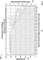
- FIG. 6 shows an example of how the performance of the SSD changes with a change of the wait time duration.
- the horizontal axis 602 shows the wait timer set to different wait time durations ranging from 24.5 microseconds to 109.5 microseconds for a read command.
- the axis 604 shows how latency in terms of data rate associated with128K sequential reads decreases as the wait time duration (also referred to as "delay to first status check") increases.
- the axis 606 shows how throughput in terms of kilo input output operations (klOPS) decreases as the wait time duration increases. This decrease becomes apparent generally after the wait time duration exceeds 84.5 microseconds.
- klOPS kilo input output operations
- Performance of the SSD similarly changes by setting the status polling timer to different polling time durations.
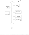
- FIG. 7 is a block diagram of an example SSD controller 102 for controlling performance of the SSD.
- the SSD controller 102 includes a processor 702 (possibly including multiple processors, multiple cores, multiple nodes, and/or implementing multi-threading, etc.).
- the SSD controller 102 includes memory 704.
- the memory 704 is system memory (e.g., one or more of cache, random access memory (RAM), synchronous RAM (SRAM), dynamic RAM (DRAM), zero capacitor RAM, Twin Transistor RAM, embedded DRAM (eDRAM), extended data output RAM (EDO RAM), double data rate RAM (DDR RAM), electrically erasable programmable read only memory (EEPROM), Nano-RAM (NRAM), resistive RAM (RRAM), silicon-oxide-nitride-oxide-silicon memory (SONOS), parameter random access memory (PRAM), etc.) or any one or more other possible realizations of non-transitory machine-readable media/medium.
- the memory 704 stores timer durations which are used to set the non-volatile memory timer.
- the stored timer durations is associated with different SSD configurations and/or different storage commands. The association facilitates identifying the timer duration associated with the current configuration of the SSD or storage access request being executed and setting the non-volatile memory timer with the identified timer duration.
- the memory 704 includes registers to store an indication of a wait time duration and/or polling time duration for setting the wait timer and status polling timer.
- the SSD controller 102 also includes a bus 706 (e.g., Peripheral Component Interconnect (PCI), Industry Standard Architecture (ISA), PCI-Express, New Bus (NuBus), etc.). Coupled to the bus 706 is interface 708 which facilitates communication with the non-volatile memory array of the SSD and the host. In this regard, the interface 708 includes the host interface and the non-volatile memory interface.
- the SSD controller 102 has a wait timer 710 and status polling timer 712.
- a timer control 714 of the SSD controller 102 implements any one of the previously described functionalities for setting the timers to control performance of the SSD partially, (or entirely) in hardware and/or software (e.g., computer code, program instructions, program code, computer instructions) stored on a non-transitory machine readable medium/media.
- the processor 702 and memory 704 implements or facilitate implementing the functionalities instead of or in addition to the timer control 714.
- realizations can include fewer or additional components not illustrated in Figure 7 (e.g., video cards, audio cards, additional network interfaces, peripheral devices, etc.).
- the processor 702 and the memory 704 are coupled to the bus 706. Although illustrated as being coupled to the bus 706, the memory 704 can be coupled to the processor 702.
- a program (also known as a computer program, software, software application, script, or code) can be written in any form of programming language, including compiled or interpreted languages, or declarative or procedural languages, and it can be deployed in any form, including as a stand alone program or as a module, component, subroutine, or other unit suitable for use in a computing environment.
- a program does not necessarily correspond to a file in a file system.
- a program can be stored in a portion of a file that holds other programs or data (e.g., one or more scripts stored in a markup language document), in a single file dedicated to the program in question, or in multiple coordinated files (e.g., files that store one or more modules, sub programs, or portions of code).
- a program can be deployed to be executed on one computer or on multiple computers that are located at one site or distributed across multiple sites and interconnected by a communication network.
Landscapes
- Engineering & Computer Science (AREA)
- Theoretical Computer Science (AREA)
- Physics & Mathematics (AREA)
- General Engineering & Computer Science (AREA)
- General Physics & Mathematics (AREA)
- Human Computer Interaction (AREA)
- Microelectronics & Electronic Packaging (AREA)
- Computer Hardware Design (AREA)
- Read Only Memory (AREA)
- Memory System (AREA)
Description
- This disclosure relates to controlling performance of a solid state drive (SSD), namely controlling latency and throughput of the SSD.
- A solid-state drive (SSD) is a data storage device that uses non-volatile memory such as NAND (Not-And) or NOR (Not-Or) non-volatile memory to store persistent digitally encoded data. The SSD is configured to emulate a hard disk drive, i.e., a device that stores persistent digitally encoded data on magnetic surfaces of rapidly rotating platters and replaces a hard disk drive (HDD) in many applications.
- A host is typically coupled to the SSD to read data from the SSD, write data to the SSD, and erase data from the SSD. To facilitate the reading, writing, and erasing of the data, the SSD has an SSD controller with a host interface for communicating with the host and a non-volatile memory interface for managing the non-volatile memory. The host interface includes addressing, a data bus, and control for communicating with the host and conforms to a data communication protocol such as Serial Advanced Technology Attachment (SATA), Serial Attached Small Computer System Interface (SAS), Non-Volatile Memory Express (NVMe) or Universal Serial Bus (USB), while the non-volatile memory interface includes addressing, a data bus, and control for managing the non-volatile memory and conforms to a data communication protocol such as open NAND flash interface (ONFI) for NAND non-volatile memory.
- The host issues write, read, and erase requests to perform a write, read, and erase operation, respectively, on the SSD. To perform the write operation, the host sends a write request to the SSD. The write request indicates data to write and a data address where to write the data. The write request is received at the host interface of the SSD. The SSD controller then executes hardware and/or firmware to write the data in the non-volatile memory based on the data address, via the non-volatile memory interface. To perform the read operation, the host sends a read request to the SSD. The read request indicates a data address to read. The read request is received at the host interface of the SSD. The SSD controller executes hardware and/or firmware to read data in the non-volatile memory based on the data address. The SSD controller receives the data that is read from the non-volatile memory via the non-volatile memory interface and provides the read data to the host via the host interface. To perform the erase operation, the host sends an erase request to the SSD. The erase request indicates a data address to erase. The erase request is received at the host interface of the SSD. The SSD controller executes hardware and/or firmware to perform an erase operation in the non-volatile memory based on the data address.
- The SSD has a latency and throughput that depends on a type of non-volatile memory used by the SSD. For example, NOR non-volatile memory might read and/or write data faster than NAND non-volatile memory. The SSD also has a latency and throughput that depends on an SSD controller implementation. SSD controllers may be designed with different firmware parameters associated with reading and/or writing data, have different non-volatile memory interface speeds, and have different host interface speeds. In this regard, SSDs using different controllers or different types of non-volatile memory will perform differently.
- A manufacturer builds SSDs with the different SSD controllers and non-volatile memory types depending on cost and/or component availability. In this regard, the SSDs from the same manufacturer will perform differently depending on components in the SSD. Because the SSDs use different components, the manufacturer cannot guarantee a same level of latency and throughput of the SSDs, even though in some situations customers might expect a same level of performance.
-
US 2009/172213 A1 discloses, performing a status read operation to determine the status of a memory command, after a hold off time following the issuance of a memory command If the memory command has not yet completed, a polling interval is used to perform a status read operation and repeating the process until the memory command has been completed. -
US 2009/089492 A1 relates to methods, systems and computer program products for implementing a polling process among one or more flash memory devices. In some implementations, the polling process may include sending a read status command to a flash memory device to detect the ready or busy state of the flash memory device. A status register may be included in the flash memory device for storing a status signal indicating an execution state of a write (or erase) operation. A solid state drive system may perform the polling process by reading the status register of the flash memory device. -
US 2016/179373 A1 relates to an apparatus which includes a register memory and circuitry. The register memory is configured to hold a minimal value specified for a performance measure of a given type of memory access commands, whose actual performance measures vary among memory devices. The circuitry is configured to receive a memory access command of the given type, to execute the received memory access command in one or more memory devices, and to acknowledge the memory access command not before reaching the minimal value stored in the register memory. - It is the object of the present invention to provide an improved adaptation of non-volatile memory access timers.
- This object is solved by the subject matter of the independent claims. Preferred embodiments of the invention are defined by the dependent claims.
- This disclosure relates to controlling performance of solid state drives (SSD), namely controlling latency and throughput of SSDs by adjusting wait time duration and/or polling time duration associated with reading, writing, and/or erasing data in the non-volatile memory of the SSD. The adjustment of the wait time duration and/or polling time duration allows for controlling performance of SSDs even though the SSDs use different SSD controller implementations or non-volatile memory types.
- According to an aspect of the described system and techniques, a method comprises receiving a storage access request to access a solid state drive (SSD); setting a non-volatile memory access timer with a time duration, wherein the time duration is based on a desired performance of the SSD; sending a non-volatile memory command associated with the storage access request to non-volatile memory; starting the non-volatile memory access timer; determining whether the non-volatile memory completed execution of the non-volatile memory command after the non-volatile memory access timer indicates that the time duration elapsed; providing an indication that the storage access request is complete if the non-volatile memory completed execution of the non-volatile memory command; and resetting the non-volatile memory access timer based on the time duration if the non-volatile memory has not completed execution of the non-volatile memory command.
- According to another aspect of the described system and techniques, a non-transitory computer-readable medium storing instructions that, when executed by one or more processors, cause the one or more processors to at least: receive a storage access request to access a solid state drive (SSD); set a non-volatile memory access timer with a time duration, wherein the time duration is based on a desired performance of the SSD; send a non-volatile memory command associated with the storage access request to non-volatile memory; start the non-volatile memory access timer; determine whether the non-volatile memory completed execution the non-volatile memory command after the non-volatile memory access timer indicates that the time duration elapsed; provide an indication that the storage access request is complete if the non-volatile memory completed execution of the non-volatile memory command; and reset the non-volatile memory access timer based on the time duration if the non-volatile memory has not completed execution of the non-volatile memory command.
- According to yet another aspect of the described system and techniques, an SSD comprises: an SSD controller having a non-volatile memory access timer; a non-volatile memory; instructions stored in memory of the SSD controller and that, when executed by one or more processors of the SSD controller, cause the SSD controller to at least: receive a storage access request to access the SSD; set the non-volatile memory access timer with a time duration, wherein the time duration is based on a desired performance of the SSD; send a non-volatile memory command associated with the storage access request to the non-volatile memory; start the non-volatile memory access timer; determine whether the non-volatile memory completed execution of the non-volatile memory command after the non-volatile memory access timer indicates that the time duration elapsed; provide an indication that the storage access request is complete if the non-volatile memory completed execution of the non-volatile memory command; and reset the non-volatile memory access timer based on the time duration if the non-volatile memory has not completed execution of the non-volatile memory command.
- In this regard, mechanisms are provided for controlling performance of SSDs.
-
-
FIG. 1 is an example solid state drive (SSD) arranged with functionality to control performance of the SSD. -
FIG. 2 is a flow chart of example functions associated with setting a non-volatile memory timer with a time duration to control performance of the SSD. -
FIG. 3 is an example of a configuration command which defines the time duration. -
FIG 4 is a flow chart of example functions associated with controlling performance of the SSD. -
FIGs. 5 and6 illustrate how setting an example non-volatile memory timer in the form of a wait timer with a wait time duration changes latency and throughput of the SSD. -
FIG. 7 is a block diagram of an example SSD controller for controlling performance of the SSD. - The drawings are for the purpose of illustrating example embodiments, but it is understood that the embodiments are not limited to the arrangements and instrumentality shown in the drawings.
- This disclosure provides examples and details for controlling performance of a solid state drive (SSD), namely controlling latency and throughput associated with read, write, and erase operations on the SSD, by controlling a wait time duration and polling time duration associated with non-volatile memory of the SSD. The latency is indicative of a delay to complete a read, write, or erase operation and the throughput is indicative of a rate by which the operations are completed. By controlling the wait time duration and the polling time duration, SSDs that use different SSD controller implementations or non-volatile memory types is arranged to have similar performance. The principles described herein is applied to controlling performance of other type of storage devices, such as a hard disk drive (HDD) or hybrid SSD/HDD drives where a storage medium is accessed.
-
FIG. 1 illustrates an example SSD arranged with functionality to control latency and throughput of the SSD. The SSD 100 includes anSSD controller 102 and non-volatile memory (NVM)array 104. The SSD 100 is coupled to ahost 106 such as a computer system for performing read, write, and erase operations on the SSD 100. - The
SSD controller 102 has a host interface 108 and a non-volatile memory interface 110. The host interface 108 facilitates communicating with thehost 106. The host interface 108 includes addressing, a data bus, and control for communicating with thehost 106 and conforms to a data communication protocol such as Serial Advanced Technology Attachment (SATA), Serial Attached Small Computer System Interface (SAS), Non-Volatile Memory Express (NVMe) or Universal Serial Bus (USB). For example, the host interface 108 receives data to be stored on theSSD 100 from thehost 106 and transmits data stored on theSSD 100 to thehost 106. The non-volatile memory interface 110 facilitates management of thenon-volatile memory array 104. The non-volatile memory interface 110 includes addressing, a data bus, and control for managing thenon-volatile memory array 104 and conforms to a data communication protocol such as open NAND ("Not-And") flash interface (ONFI) for NAND flash. TheSSD controller 102 facilitates performing read, write, and erase operations on thenon-volatile memory array 104. - During a write operation, the
host 106 writes data to theSSD 100. TheSSD controller 102 receives this data from thehost 106 via a write request which also identifies a logical block address (LBA) where to write the data. TheSSD controller 102 maps the LBA to a physical address in thenon-volatile memory array 104 and cause thenon-volatile memory array 104 to write the data to the corresponding physical address. TheSSD 100 has one or more ofvolatile memory 120,nonvolatile memory 122, or other memory (e.g., memory within the SSD controller) to store mapping information that associates an LBA with a physical address. - During a read operation, the
host 106 reads data from theSSD 100. For example, thehost 106 sends a read request to theSSD controller 102 with a logical block address (LBA) where to read the data. TheSSD controller 102 receives the read request from thehost 106. TheSSD controller 102 maps the LBA to a physical address in thenon-volatile memory array 104 and cause thenon-volatile memory array 104 to read the data from the corresponding physical address and provide it to theSSD controller 102. TheSSD controller 102 then provides the read data to thehost 106 via the host interface 108. - During an erase operation, the
host 106 erases data from theSSD 100. For example, the host sends an erase request to theSSD controller 102 with an LBA where data is to be erased. TheSSD controller 102 receives the erase request from thehost 106. TheSSD controller 102 maps the LBA to a physical address in thenon-volatile memory array 104 and cause thenon-volatile memory array 104 to erase the data from the corresponding physical address in thenon-volatile memory array 104. - The
non-volatile memory array 104 includes one or more non-volatile memory 112-1, 112-2, 112-3 ... 112-n, referred to collectively asnon-volatile memory 104 or thenon-volatile memory array 104. In some examples, each non-volatile memory 112-1...112-n store data in a plurality of blocks, and each of the blocks includes a plurality of addressable s pages. Each of the addressable pages is a physical memory location that corresponds to a physical address, which in turn is associated with an LBA. Accordingly, each LBA written to or read by thehost 106 corresponds to a physical location in one of the non-volatile memories 112-1...1 12-n that is accessed according to one of the addressable pages. Thenon-volatile memory array 104 implements NAND non-volatile memory, NOR (Not-Or) non-volatile memory, a combination of NAND and NOR non-volatile memory, or other types of storage media. - The
SSD controller 102 also has one or more non-volatile memory timers, shown as await timer 114 andstatus polling timer 116. The non-volatile memory timer is set with a given time duration and provide an indication when the given time duration has elapsed after starting the non-volatile memory timer. For example, the non-volatile memory timer is set with the given time duration (e.g., 80 microseconds) and the non-volatile memory timer started. The non-volatile memory timer has a counter or timer for determining that the given time duration elapsed since when the non-volatile memory timer was started. After the time duration elapsed, the non-volatile memory timer provides the indication. - The non-volatile memory timer in the form of the
wait timer 114 andstatus polling timer 116 are used to facilitate reading, writing, and/or erase operations in thenon-volatile memory array 104. Thewait timer 114 and status-polling timer 116 is set to a respective time duration and started when a read, write, or erase command is issued to thenon-volatile memory 104 array as part of the read, write, or erase operation. Thewait timer 114 andstatus polling timer 116 provides respective indications when the respective time duration has elapsed. After the time duration of thewait timer 114 and/orstatus polling timer 116 elapses,SSD controller 102 performs a status polling to determine completion of the read, write, or erase command by thenon-volatile memory array 104. If theSSD controller 102 determines that the read, write, or erase command is complete, then SSD provides an indication to thehost 106 via the host interface 108 that the read, write, or erase operation is complete. Otherwise, thewait timer 114 andstatus polling timer 116 is reset and theSSD controller 102 performs additional status polling requests based on thewait timer 114 andstatus polling timer 116 until the read, write, or erase command is complete. - In examples, the
SSD controller 102 has atimer controller 124 to facilitate setting thewait timer 114 and/orstatus polling timer 116 with the time duration to control performance of theSSD 100, such as latency and/or throughput, during storage operations such as the read, write, or erase operation. The latency is indicative of a delay to complete the read, write, or erase operation and the throughput is indicative of a rate by which the read, write, or erase operation is completed. Setting thewait timer 114 and/orstatus polling timer 116 with a longer time duration results in a longer latency and/or less throughput of theSSD 100. Setting thewait timer 114 and/orstatus polling timer 116 with a shorter time duration results in a shorter latency and/or more throughput of theSSD 100.SSD controller 102 is shown to have both await timer 114 andstatus polling timer 116, but in some examples, theSSD controller 102 has one or the other timer, or additional timers. In other examples, thewait timer 114 andstatus polling timer 116 is located on other systems of theSSD 100. - Setting the non-volatile memory access timer with the given time duration allows for artificially tuning the SSD to meet performance criteria such as a latency and/or throughput of the SSD. The given time duration is set in many ways, examples of which are provided below.
- In various examples, the given time duration of the non-volatile memory access timer is set based on a configuration of the SSD such as the non-volatile memory in the SSD or SSD controller implementation. For example, an SSD with NOR non-volatile memory might read and/or write data faster than an SSD with NAND non-volatile memory. If the SSD has a NAND non-volatile memory, the time duration is set to one time value stored in the
SSD controller 102 while if the SSD has a NOR non-volatile memory, the time duration is set to another time value stored in theSSD controller 102 to achieve a desired performance of the SSD for the configuration of the SSD. As another example, SSD controllers is designed with different firmware parameters associated with reading and/or writing data, have different non-volatile memory interface speeds, and have different host interface speeds. The wait timer and/or polling timer is set with respective time durations to achieve a desired performance of the SSD for the configuration of the SSD controller. - For example, the SSD controller stores a mapping of different host interface speeds, non-volatile memory interface speeds, and/or firmware parameters of the SSD to different time durations. Based on a current host interface speed, non-volatile memory interface speed, and/or firmware parameters of the SSD, the SSD controller identifies the mapped time durations and set the wait timer and/or status polling timer with the time durations. The polling time duration and/or wait time duration is increased to increase latency and decrease throughput while the polling time duration and/or wait time duration is decreased to decrease latency and increase throughput to achieve a desired performance of the SSD for the configuration of the SSD. In this regard, latency and/or throughput of the SSD is artificially controlled by changing one or more of the polling time duration and wait time duration. Further, by controlling the wait time duration and the polling time duration, SSDs that use different SSD controller implementations or non-volatile memory is arranged to have similar performance. For example, if one SSD has different components than another SSD, one or more of the polling time duration and wait time duration for each SSD is set so that performance of each SSD is similar despite use of the different components.
- In various examples, the wait time duration and/or polling time duration is set based on a storage access request. For example, the storage access request is a read request to read data stored in the SSD, a write request to write data to the SSD, or an erase request to erase data in the SSD. The time duration is set so that the SSD meets performance criteria associated with the SSD.
-
FIG. 2 is a flow chart of example functions associated with setting the wait time duration and/or polling time duration to control performance of the SSD based on the storage access request. The functions is implemented by the SSD controller in hardware, firmware, and/or a combination of hardware and firmware. - At 202, a storage access request is received. The storage access request is received from a host at a host interface of the SSD controller.
- At 204, a determination is made as to the type of the storage access request that is received. The storage access request is a read request, write request or erase request. Each type of storage access request is associated with a given time duration associated with the wait timer and status polling timer such as a respective wait time duration and polling time duration stored in the SSD controller.
- At 206, the non-volatile memory access timer is set with a time duration based on the type of the storage access request. For example, if the type of storage access request is a write request and the non-volatile memory access timer is a status polling timer, then the status polling timer is set to a polling time duration stored in the SSD controller which is associated with the write request. As another example, if the type of storage access request is a write request and the non-volatile memory access timer is a wait timer, then the wait timer is set to a wait time duration stored in the SSD controller which is associated with the write request. The wait timer and status polling timer is similarly set to the respective wait time duration and polling time duration associated with the read request or erase request if the storage access request is a read request or erase request. In some examples, the wait time duration is the same for each of the requests and the polling time duration differs.
- In various examples, the wait time duration and/or polling time duration is defined by a configuration command. The configuration command is indicative of a desired performance of the SSD.
-
FIG. 3 is an example of a configuration command that might be used to set the time duration. Theconfiguration command 300 is sent from the host or generated by the SSD controller. Theconfiguration command 300 includes atype field 302 and atimer field 310. Thetype field 302 indicates that the command is a configuration command by a unique code such as string of bits. Thetimer field 310 defines one or more time durations. As illustrated, thetimer field 310 takes the form of one or more of a waittime duration field 304 and a pollingtime duration field 306, both of which are shown in theconfiguration command 300. The waittime duration field 304 and a pollingtime duration field 306 indicates the wait time duration and polling time duration associated with the wait timer and status polling timer, respectively. Based on identification of the configuration command by the type field, the SSD controller sets the respective non-volatile memory timer with the time durations in thetimer field 310. For example, the wait timer is set with the wait time duration in the waittime duration field 304 and the status polling timer is set with the polling time duration in the pollingtime duration field 306. - In some examples, the SSD controller stores an indication of a preset polling time duration and preset wait time duration in memory which is then accessed and associated with the status polling timer and wait timer respectively. The configuration command provides an indication to select a particular preset polling time duration and preset wait time duration from a plurality of options stored on the SSD controller rather than specifying an actual polling time duration and wait time duration in the configuration command itself. This way firmware overhead for obtaining the wait time duration or polling time duration is reduced since the time durations are already stored locally, for example, in a register of the SSD controller.
-
FIG 4 is anexample flow chart 400 of example functions associated with controlling performance of the SSD by setting the wait timer and/or status polling timer associated with storage operations. The functions implements on the SSD controller in firmware, hardware, or a combination of firmware and hardware. Setting the wait timer and/or status polling timer with a given time duration allows for artificially tuning the SSD to meet performance criteria such as a latency and/or throughput of the SSD. - At 402, the SSD controller receives a storage access request from the host. The host interface of the SSD controller receives the storage access request. The storage access request takes many forms. For example, the storage access request is the read request with an indication of a logical address associated with the data to be read. As another example, the storage access operation is the write request with an indication of the data to write to the SSD and the logical address where the data is to be written. As another example, the storage access operation is an erase request with an indication of the logical address having the data to be erased. The storage access request takes other forms as well.
- At 404, the SSD controller sets a non-volatile memory access timer with a given time duration, where the given time duration is based on a desired performance of the SSD. The non-volatile memory access timer takes the form of the wait timer and/or status polling timer. The wait timer and status polling timer is set with a respective wait time duration and polling time duration to control the performance of the SSD. The respective wait time duration and polling time duration is determined in many ways as described above. The setting of the wait timer and status polling timer with the respective wait time duration and polling time duration artificially tunes the SSD to meet performance criteria such as a latency and/or throughput of the SSD.
- At 406, the SSD controller sends a non-volatile memory command to the non-volatile memory array based on the storage access request. For example, a read command identifies the physical address in the non-volatile memory to be read which corresponds to the logical address to be read, indicated by the read request. As another example, a write command identifies
- the physical address in the non-volatile memory to be written to which corresponds to the logical address to be written to and the data to write, indicated by the write request. In yet another example, an erase command identifies the physical address in the non-volatile memory to be erased which corresponds to the logical address to be erased, indicated by the erase request. After the non-volatile memory command is sent, at 408, the SSD controller starts
- the wait timer and wait for the wait time duration before performing status polling of the non-volatile memory array to determine if execution of the non-volatile memory command is completed by the non-volatile memory array. It is recommended to wait for a certain period of time before checking whether execution of the command is complete because if too many status pollings are issued, bandwidth of the non-volatile memory array is not efficiently utilized. In this regard, the wait timer indicates whether the status polling should be performed. For example, wait timer is set to the time duration equal to the wait time duration and started. The wait timer indicates that the time associated with the wait time duration has elapsed, at which point the status polling should be performed, and not performed otherwise.
- At 410, the SSD controller performs the status polling after the wait time duration elapses. The status polling is a check on a status of whether the non-volatile memory array has completed execution of the non-volatile memory command. The status polling takes the form of checking a register in the non-volatile memory which indicates whether the execution is complete. As another example, the status polling takes the form of sending a status message to the non-volatile memory requesting an indication whether the execution is complete.
- At 412, a response to the status polling is received and, at 414, the response to the status polling is checked. The response is a message from the non-volatile memory which indicates whether execution is complete or a result of checking the register which indicates whether execution is complete. If the response indicates that execution of the non-volatile memory command is complete, then at 416, an indication is provided to the host that the storage access request is complete. For example, if the non-volatile memory command is a read command, then the execution is complete when the data to be read is available to the SSD controller. As another example, if the non-volatile memory command is a write command, then the execution is complete when the data is written to the non-volatile memory. In yet another example, if the non-volatile memory command is an erase command, then the execution is complete when the data to be erased is erased by the non-volatile memory. If the non-volatile memory command is a read command, the SSD controller requests the read data from the non-volatile memory which is provided to the SSD controller. The indication to the host is the data that is read. For write or erase requests, the indication is a message or status indication that the respective write or erase request has been performed.
- In some examples, the non-volatile memory array has not completed execution of the non-volatile memory command even after the SSD controller performs the initial status polling. In such a case, the SSD controller performs additional status polling requests. The status polling timer controls how frequently the controller shall issue the additional status polling requests.
- The status polling timer is set to the time duration equal to the polling time duration at 404. At 418, the SSD controller starts the status polling timer and wait for the polling time duration to elapse. At 420, the status polling timer indicates that the polling time duration has elapsed, at which point the status polling is performed, and not performed otherwise. After the status polling is performed, processing continues to 412.
Blocks block 416. - In some examples, block 418 includes setting the status polling timer with the polling time duration before starting the status polling timer if the status polling timer is not set with the polling time duration before being started. In some examples, the SSD controller varies
the polling time duration after one or more times the status polling timer is reset for the storage access operation. For instance, the SSD controller has a counter which counts how many times the status polling has been performed for the storage access request. The status polling timer duration is increased and/or decreased based on the count so that performance criteria is met and latency and/or throughput of the SSD is fine tuned. - The time duration which the wait timer and status polling timer are set allows for controlling a latency and throughput of the SSD. For example, setting the wait timer to a longer wait time duration and/or setting the status polling timer to a longer polling time duration increases
a time to perform the storage access operation. As another example, setting the wait timer to a shorter wait time duration and/or setting the status polling timer to a shorter polling time duration decreases a time to perform the storage access operation. This way performance of the SSD is adjusted for various SSD controller and/or non-volatile memory configurations so that performance across a plurality of SSDs is the same or different. -
FIG. 5 illustrates graphically how the setting of the wait time duration of the wait timer might change latency and/or throughput performance of the SSD. Two message flows 530 and 550 are shown as a result of issuing aread command 502. Ahorizontal axis 500 indicates time. -
Message flow 530 is associated with a first wait time duration. At 502, a read request is received and at 504, an address associated with the data to read is received. The wait timer is set with the wait time duration. The read command is issued to the non-volatile memory array and at 506, a status polling performed at T1 after the wait timer indicates that the wait time duration has elapsed. A response to the status polling performed at T1 indicates that the read command has been completed. If execution of the read operation is complete, then the SSD controller requests that the non-volatile memory array provide the data to be read which is received at T2. An example of the request is shown as "05h, Address, E0h" which results indata 508 being received. - If the wait time duration is increased, then the latency and performance of the SSD increases.
Message flow 550 is associated with a second wait time duration longer than the first wait time duration. At 510, a read request is received and at 512, an address associated with the data to read is received. The wait timer is set with the wait time duration which is longer than the wait time duration described in theflow 530. The read command is issued to the non-volatile memory array and at 514, a status polling performed at T3 after the wait timer indicates that the wait time duration elapsed. T3 is after T1, indicating that the wait time is longer. A response to the status polling performed at T3 indicates that the read command has been completed. If execution of the read operation is complete, then the SSD controller requests that the non-volatile memory array provide the data to be read which is received at T4. An example of the request is shown as "05h, Address, E0h" which results indata 516 being received. - In
message flow 550, the data is not received until T4 which is longer than T2 because the time associated with the wait time duration is longer. In this regard, a wait time duration associated with wait timer is directly related to a read time (tRead) and latency and/or throughput of reading data from the SSD. Similarly, a polling time duration associated with the status polling timer (not shown) is directly related to the latency and throughput of reading data from the SSD. For example, one or more status polling requests is sent to the non-volatile memory, each separated by a polling time duration until the read operation is complete. Further, the wait time duration and polling time duration are directly related to latency and throughput of writing and erasing data in the SSD. -
FIG. 6 shows an example of how the performance of the SSD changes with a change of the wait time duration. Thehorizontal axis 602 shows the wait timer set to different wait time durations ranging from 24.5 microseconds to 109.5 microseconds for a read command. Theaxis 604 shows how latency in terms of data rate associated with128K sequential reads decreases as the wait time duration (also referred to as "delay to first status check") increases. Theaxis 606 shows how throughput in terms of kilo input output operations (klOPS) decreases as the wait time duration increases. This decrease becomes apparent generally after the wait time duration exceeds 84.5 microseconds. In this regard, adjusting the wait time duration allows for configuration of the latency and/or throughput of the SSD. Performance of the SSD similarly changes by setting the status polling timer to different polling time durations. -
FIG. 7 is a block diagram of anexample SSD controller 102 for controlling performance of the SSD. TheSSD controller 102 includes a processor 702 (possibly including multiple processors, multiple cores, multiple nodes, and/or implementing multi-threading, etc.). TheSSD controller 102 includesmemory 704. Thememory 704 is system memory (e.g., one or more of cache, random access memory (RAM), synchronous RAM (SRAM), dynamic RAM (DRAM), zero capacitor RAM, Twin Transistor RAM, embedded DRAM (eDRAM), extended data output RAM (EDO RAM), double data rate RAM (DDR RAM), electrically erasable programmable read only memory (EEPROM), Nano-RAM (NRAM), resistive RAM (RRAM), silicon-oxide-nitride-oxide-silicon memory (SONOS), parameter random access memory (PRAM), etc.) or any one or more other possible realizations of non-transitory machine-readable media/medium. In examples, thememory 704 stores timer durations which are used to set the non-volatile memory timer. In examples, the stored timer durations is associated with different SSD configurations and/or different storage commands. The association facilitates identifying the timer duration associated with the current configuration of the SSD or storage access request being executed and setting the non-volatile memory timer with the identified timer duration. In some examples, thememory 704 includes registers to store an indication of a wait time duration and/or polling time duration for setting the wait timer and status polling timer. - The
SSD controller 102 also includes a bus 706 (e.g., Peripheral Component Interconnect (PCI), Industry Standard Architecture (ISA), PCI-Express, New Bus (NuBus), etc.). Coupled to thebus 706 isinterface 708 which facilitates communication with the non-volatile memory array of the SSD and the host. In this regard, theinterface 708 includes the host interface and the non-volatile memory interface. TheSSD controller 102 has await timer 710 andstatus polling timer 712. - A
timer control 714 of theSSD controller 102 implements any one of the previously described functionalities for setting the timers to control performance of the SSD partially, (or entirely) in hardware and/or software (e.g., computer code, program instructions, program code, computer instructions) stored on a non-transitory machine readable medium/media. In some instances, theprocessor 702 andmemory 704 implements or facilitate implementing the functionalities instead of or in addition to thetimer control 714. Further, realizations can include fewer or additional components not illustrated inFigure 7 (e.g., video cards, audio cards, additional network interfaces, peripheral devices, etc.). Theprocessor 702 and thememory 704 are coupled to thebus 706. Although illustrated as being coupled to thebus 706, thememory 704 can be coupled to theprocessor 702. - A few implementations have been described in detail above, and various modifications are possible. The disclosed subject matter, including the functional operations described in this specification, can be implemented in electronic circuitry, computer hardware, firmware, software, or in combinations of them, such as the structural means disclosed in this specification and structural equivalents thereof: including potentially a program operable to cause one or more data processing apparatus such as a processor to perform the operations described (such as a program encoded in a non-transitory computer-readable medium, which can be a memory device, a storage device, a machine-readable storage substrate, or other physical, machine readable medium, or a combination of one or more of them).
- A program (also known as a computer program, software, software application, script, or code) can be written in any form of programming language, including compiled or interpreted languages, or declarative or procedural languages, and it can be deployed in any form, including as a stand alone program or as a module, component, subroutine, or other unit suitable for use in a computing environment. A program does not necessarily correspond to a file in a file system. A program can be stored in a portion of a file that holds other programs or data (e.g., one or more scripts stored in a markup language document), in a single file dedicated to the program in question, or in multiple coordinated files (e.g., files that store one or more modules, sub programs, or portions of code). A program can be deployed to be executed on one computer or on multiple computers that are located at one site or distributed across multiple sites and interconnected by a communication network.
- While this specification contains many specifics, these should not be construed as limitations on the scope of what is claimed, but rather as descriptions of features that is specific to particular implementations. Certain features that are described in this specification in the context of separate implementations can also be implemented in combination in a single implementation. Conversely, various features that are described in the context of a single implementation can also be implemented in multiple implementations separately or in any suitable subcombination. Moreover, although features is described above as acting in certain combinations and even initially claimed as such, one or more features from a claimed combination can in some cases be excised from the combination, and the claimed combination is directed to a subcombination or variation of a subcombination.
- Similarly, while operations are depicted in the drawings in a particular order, this should not be understood as requiring that such operations be performed in the particular order shown or in sequential order, or that all illustrated operations be performed, to achieve desirable results. In certain circumstances, multitasking and parallel processing is advantageous. Moreover, the separation of various system components in the implementations described above should not be understood as requiring such separation in all implementations.
Claims (15)
- A method for controlling a time to execute a storage access request in a solid state drive, SSD, (100) to achieve a performance of the SSD similar to a performance of another SSD, the time being based on a configuration of the SSD (100) and on the performance of the another SSD (100), the SSD (100) having non-volatile memory and a controller (102), the method comprising:storing in the controller (102) time values and associating the time values with different SSD (100) configurations;receiving, by the controller (102), the storage access request to access the SSD (100);setting, by the controller (102), a non-volatile memory access timer with a time duration which controls the time to execute the storage access request, wherein the time duration is defined by;the performance of the other SSD, andthe configuration of the SSD (100), including setting the non-volatile memory access timer with a first time value of the time values stored in the controller (102) if the non-volatile memory of the SSD (100) is a NAND non-volatile memory, and setting the non-volatile memory access timer with a second time value stored in the controller (102) if the non-volatile memory of the SSD (100) is a NOR non-volatile memory;sending, by the controller (102), a non-volatile memory command associated with the storage access request to the non-volatile memory;starting, by the controller (102), the non-volatile memory access timer based on the non-volatile memory command being sent to the non-volatile memory;after the non-volatile memory access timer indicates that the time duration elapsed determining, by the controller (102), whether or not the non-volatile memory completed execution of the non-volatile memory command;if the non-volatile memory is determined to have completed execution of the non-volatile memory command, providing, by the controller (102), an indication that the storage access request is complete; andif the non-volatile memory is determined not to have completed execution of the non-volatile memory command, repeating resetting, by the controller (102), the non-volatile memory access timer with the time duration and determining whether or not the non-volatile memory completed execution of the non-volatile memory command until the non-volatile memory completes the execution of the non-volatile memory command.
- The method of claim 1, wherein the non-volatile memory command is a read, write, or erase operation and the type of the received storage access request is a read, write, or erase request.
- The method of claim 1 or 2, wherein the non-volatile memory access timer includes a wait timer and a status polling timer, wherein resetting the non-volatile memory access timer comprises resetting the status polling timer with a polling time duration associated with the status polling timer, wherein the polling time duration is adjusted each time the status polling timer is reset.
- The method of one of claims 1 to 3, wherein the time duration is a wait time duration until a status polling is sent to the non-volatile memory to determine if execution of the non-volatile memory command is complete or a polling time duration until another status polling is sent to the non-volatile memory to determine if execution of the non-volatile memory command is complete, wherein the polling time duration is adjusted for different types of non-volatile memory commands.
- The method of one of claims 1 to 4, wherein setting the non-volatile memory access timer with a time duration comprises receiving a configuration command, wherein the configuration command includes a time duration field; and setting the time duration based on a given time duration in the time duration field.
- The method of one of claims 1 to 5, wherein time duration is further based on one or more of a type of the received storage access request and a configuration of the SSD (100).
- The method of one of claims 1 to 6, wherein setting the non-volatile memory access timer with the time duration comprises increasing the time duration from a previously set time duration to increase time to perform the storage request.
- A non-transitory computer-readable medium for controlling a time to execute a storage
access request in a solid state drive, SSD, (100) to achieve a performance of the SSD similar to a performance of another SSD, the time being based on a configuration of the SSD (100) and on the performance of the another SSD, the non-transitory computer-readable medium storing instructions that, when executed by one or more processors, cause the one or more processors to at least:store in a controller (102) time values and associate the time values with different SSD (100) configurations;receive, by the controller (102), a storage access request to access an SSD (100);set, by the controller (102), a non-volatile memory access timer with a time duration which controls the time to execute the storage access request, wherein the time duration is defined by:the performance of the other SSD, andthe configuration of the SSD (100), including setting the non-volatile memory access timer with a first time value of the time values stored in the controller (102) if the non-volatile memory of the SSD (100) is a NAND non-volatile memory, and setting the non-volatile memory access timer with a second time value stored in the controller (102) if the non-volatile memory of the SSD (100) is a NOR non-volatile memory;send, by the controller (102), a non-volatile memory command associated with the storage access request to non-volatile memory;start, by the controller (102), the non-volatile memory access timer based on the non-volatile memory command being sent to the non-volatile memory;after the non-volatile memory access timer indicates that the time duration elapsed, determine, by the controller (102), whether the non-volatile memory completed execution the non-volatile memory command;if the non-volatile memory is determined to have completed execution of the non-volatile memory command, provide, by the controller (102), an indication that the storage access request is complete; andif the nonvolatile memory is determined not to have completed execution of the non-volatile memory command, repeat resetting, by the controller (102), the non-volatile memory access timer based on the time duration and determining whether or not the non-volatile memory completed execution of the non-volatile memory command until the non-volatile memory completes the execution of the non-volatile memory command. - The non-transitory computer-readable medium of claim 8, wherein the non-volatile memory command is a read, write, or erase operation and the type of the received storage access request is a read, write, or erase request.
- The non-transitory computer-readable medium of claim 8 or 9, wherein the non-volatile memory access timer includes a wait timer and a status polling timer, wherein the instructions for resetting the non-volatile memory access timer comprises instructions for resetting the status polling timer with a polling time duration associated with the status polling timer, wherein the polling time duration is adjusted each time the status polling timer is reset.
- The non-transitory computer-readable medium of one of claims 8 to 10, wherein the time duration is a wait time duration until a status polling is sent to the non-volatile memory to determine if execution of the non-volatile memory command is complete or a polling time duration until another status polling is sent to the non-volatile memory to determine if execution of the non-volatile memory command is complete, wherein the polling time duration is adjusted for different types of non-volatile memory commands.
- The non-transitory computer-readable medium of one of claims 8 to 11, wherein the instructions for setting the non-volatile memory access timer with a time duration comprises instructions for receiving a configuration command, wherein the configuration command includes a time duration field; and setting the time duration based on a given time duration in the time duration field; or
wherein the time duration is further based on one or more of a type of the received storage access request and a configuration of the SSD (100). - The non-transitory computer-readable medium of claim 8, wherein the instructions for setting the non-volatile memory access timer with the time duration comprises instructions for increasing the time duration from a previously set time duration to increase time to perform the storage request.
- A solid state device, SSD, (100) controllable to achieve a performance of the SSD similar to a performance of another SSD, the SSD comprising:an SSD controller (102) having a non-volatile memory access timer;a non-volatile memory;instructions stored in memory of the SSD controller (102) and that, when executed by one or more processors of the SSD controller (102), cause the SSD controller (102) to at least:store in the controller (102) time values and associate the time values with different SSD (100) configurations;receive a storage access request to access the SSD (100);set the non-volatile memory access timer with a time duration which controls a time to execute the storage access request, wherein the time duration is defined by:the performance of the other SSD, anda configuration of the SSD (100) including setting the non-volatile memory access timer with a first time value of the time values stored in the controller (102) if the non-volatile memory of the SSD (100) is a NAND non-volatile memory, and setting the non-volatile memory access timer with a second time value stored in the controller (102) if the non-volatile memory of the SSD (100) is a NOR non-volatile memory;send a non-volatile memory command associated with the storage access request to the non-volatile memory;start the non-volatile memory access timer based on the non-volatile memory command being sent to the non-volatile memory;after the non-volatile memory access timer indicates that the time duration elapsed, determine whether the non-volatile memory completed execution of the non-volatile memory command;if the non-volatile memory completed execution of the non-volatile memory command, provide an indication that the storage access request is complete; and if the non-volatile memory has not completed execution of the non-volatile memory command, repeat resetting the non-volatile memory access timer based on the time duration and determining whether or not the non-volatile memory completed execution of the non-volatile memory command until the non-volatile memory completes the execution of the non-volatile memory command.
- The SSD (100) of claim 14, wherein the non-volatile memory command is a read, write, or erase operation and the type of the received storage access request is a read, write, or erase request; orwherein the non-volatile memory access timer includes a wait timer and a status polling timer, wherein the instructions for resetting the non-volatile memory access timer comprises instructions for resetting the status polling timer with a polling time duration associated with the status polling timer, wherein the polling time duration is adjusted each time the status polling timer is reset; orwherein the time duration is a wait time duration until a status polling is sent to the non-volatile memory to determine if execution of the non-volatile memory command is complete or a polling time duration until another status polling is sent to the non-volatile memory to determine if execution of the non-volatile memory command is complete, wherein the polling time duration is adjusted for different types of non-volatile memory commands; orwherein the time duration is based on one or more of a type of the received storage access request and a configuration of the SSD (100); orwherein the instructions for setting the non-volatile memory access timer with the time duration comprises instructions for increasing the time duration from a previously set time duration to increase time to perform the storage request.
Applications Claiming Priority (2)
| Application Number | Priority Date | Filing Date | Title |
|---|---|---|---|
| US201862712804P | 2018-07-31 | 2018-07-31 | |
| US16/525,105 US11366753B2 (en) | 2018-07-31 | 2019-07-29 | Controlling performance of a solid state drive |
Publications (2)
| Publication Number | Publication Date |
|---|---|
| EP3605341A1 EP3605341A1 (en) | 2020-02-05 |
| EP3605341B1 true EP3605341B1 (en) | 2024-10-02 |
Family
ID=67658331
Family Applications (1)
| Application Number | Title | Priority Date | Filing Date |
|---|---|---|---|
| EP19189312.2A Active EP3605341B1 (en) | 2018-07-31 | 2019-07-31 | Controlling performance of a solid state drive |
Country Status (4)
| Country | Link |
|---|---|
| US (1) | US11366753B2 (en) |
| EP (1) | EP3605341B1 (en) |
| KR (1) | KR102883186B1 (en) |
| CN (1) | CN110780807B (en) |
Families Citing this family (11)
| Publication number | Priority date | Publication date | Assignee | Title |
|---|---|---|---|---|
| US11366753B2 (en) * | 2018-07-31 | 2022-06-21 | Marvell Asia Pte Ltd | Controlling performance of a solid state drive |
| US11249536B2 (en) * | 2018-12-17 | 2022-02-15 | Qualcomm Incorporated | Reducing power consumption of communication interfaces by clock frequency scaling and adaptive interleaving of polling |
| US11199995B2 (en) * | 2019-11-19 | 2021-12-14 | Micron Technology, Inc. | Time to live for load commands |
| US11243804B2 (en) | 2019-11-19 | 2022-02-08 | Micron Technology, Inc. | Time to live for memory access by processors |
| CN111078146B (en) * | 2019-12-13 | 2023-11-14 | 合肥兆芯电子有限公司 | Memory management method, memory storage device and memory control circuit unit |
| US11106366B1 (en) * | 2020-05-06 | 2021-08-31 | SK Hynix Inc. | Maintaining consistent write latencies in non-volatile memory devices |
| US11422825B2 (en) * | 2020-12-30 | 2022-08-23 | Kioxia Corporation | Determination of power-off duration of NVMe SSD |
| CN114385082A (en) * | 2021-12-31 | 2022-04-22 | 北京得瑞领新科技有限公司 | Data processing method of NOR flash memory, storage medium and SSD device |
| TWI813311B (en) * | 2022-05-25 | 2023-08-21 | 瑞昱半導體股份有限公司 | Nand flash memory controller |
| US12455703B2 (en) * | 2022-06-29 | 2025-10-28 | Micron Technology, Inc. | Monitoring and exporting command execution times in a semiconductor device |
| KR20240015247A (en) | 2022-07-27 | 2024-02-05 | 에스케이하이닉스 주식회사 | Data coding device, memory controller and storage device |
Citations (1)
| Publication number | Priority date | Publication date | Assignee | Title |
|---|---|---|---|---|
| US20160179373A1 (en) * | 2014-12-18 | 2016-06-23 | Apple Inc. | Hardware-based performance equalization for storage devices |
Family Cites Families (24)
| Publication number | Priority date | Publication date | Assignee | Title |
|---|---|---|---|---|
| US20050165909A1 (en) * | 2003-12-19 | 2005-07-28 | Cromer Daryl C. | Data processing system and method for permitting a server to remotely access asset information of a mobile client |
| US8438356B2 (en) * | 2007-10-01 | 2013-05-07 | Marvell World Trade Ltd. | Flash memory controller |
| US20090172213A1 (en) * | 2007-12-31 | 2009-07-02 | Sowmiya Jayachandran | Command completion detection in a mass storage device |
| US9740517B2 (en) * | 2008-12-29 | 2017-08-22 | Microsoft Technology Licensing, Llc | Dynamic virtual machine memory management |
| US8078796B2 (en) * | 2009-04-14 | 2011-12-13 | Micron Technology, Inc. | Method for writing to and erasing a non-volatile memory |
| US9582222B2 (en) * | 2009-04-30 | 2017-02-28 | Western Digital Technologies, Inc. | Pre-cache similarity-based delta compression for use in a data storage system |
| CN101872320A (en) * | 2010-04-16 | 2010-10-27 | 浪潮电子信息产业股份有限公司 | A kind of test and statistical method about reliability and performance of SSD hard disk |
| US8737138B2 (en) * | 2010-11-18 | 2014-05-27 | Micron Technology, Inc. | Memory instruction including parameter to affect operating condition of memory |
| US20160029402A1 (en) * | 2010-11-22 | 2016-01-28 | Seven Networks, Llc | Optimization of resource polling intervals to satisfy mobile device requests |
| US20120278819A1 (en) * | 2011-04-26 | 2012-11-01 | Byungcheol Cho | Polling-driven device driver interface |
| US8650353B2 (en) * | 2011-07-01 | 2014-02-11 | Intel Corporation | Apparatus, system, and method for refreshing non-volatile memory |
| JP5722264B2 (en) * | 2012-03-23 | 2015-05-20 | 株式会社日立ハイテクノロジーズ | Data processing apparatus and data capacity increase suppressing method |
| US9519590B1 (en) * | 2012-06-26 | 2016-12-13 | EMC IP Holding Company LLC | Managing global caches in data storage systems |
| US20160054779A1 (en) * | 2014-08-22 | 2016-02-25 | Devadatta Bodas | Managing power performance of distributed computing systems |
| KR102306804B1 (en) * | 2015-01-21 | 2021-09-30 | 삼성전자주식회사 | Method and apparatus for reducing power consumption of electronic device |
| US9924406B2 (en) * | 2015-03-02 | 2018-03-20 | Verizon Patent And Licensing Inc. | Blended data transmission network for machine type communications |
| JP2016212511A (en) * | 2015-04-30 | 2016-12-15 | 富士通株式会社 | Storage controller, storage control method and program |
| US10664257B2 (en) * | 2015-05-06 | 2020-05-26 | Apple Inc. | Secure element activities |
| US9760392B1 (en) * | 2015-08-31 | 2017-09-12 | Veritas Technologies Llc | Adaptive throttling in hybrid storage environments |
| US10547559B2 (en) * | 2015-12-26 | 2020-01-28 | Intel Corporation | Application-level network queueing |
| US10360099B2 (en) * | 2017-04-28 | 2019-07-23 | Netapp Inc. | Object format resilient to remote object store errors |
| US10909051B2 (en) * | 2017-06-01 | 2021-02-02 | Seagate Technology Llc | NAND flash reset control |
| US10909040B2 (en) * | 2018-04-19 | 2021-02-02 | Intel Corporation | Adaptive calibration of nonvolatile memory channel based on platform power management state |
| US11366753B2 (en) * | 2018-07-31 | 2022-06-21 | Marvell Asia Pte Ltd | Controlling performance of a solid state drive |
-
2019
- 2019-07-29 US US16/525,105 patent/US11366753B2/en active Active
- 2019-07-31 KR KR1020190093042A patent/KR102883186B1/en active Active
- 2019-07-31 EP EP19189312.2A patent/EP3605341B1/en active Active
- 2019-07-31 CN CN201910700563.4A patent/CN110780807B/en active Active
Patent Citations (1)
| Publication number | Priority date | Publication date | Assignee | Title |
|---|---|---|---|---|
| US20160179373A1 (en) * | 2014-12-18 | 2016-06-23 | Apple Inc. | Hardware-based performance equalization for storage devices |
Also Published As
| Publication number | Publication date |
|---|---|
| EP3605341A1 (en) | 2020-02-05 |
| KR102883186B1 (en) | 2025-11-10 |
| US11366753B2 (en) | 2022-06-21 |
| KR20200014241A (en) | 2020-02-10 |
| US20200042443A1 (en) | 2020-02-06 |
| CN110780807A (en) | 2020-02-11 |
| CN110780807B (en) | 2025-03-25 |
Similar Documents
| Publication | Publication Date | Title |
|---|---|---|
| US11366753B2 (en) | Controlling performance of a solid state drive | |
| US9741436B2 (en) | Dynamically controlling an operation execution time for a storage device | |
| US10430331B2 (en) | Reconstruct drive for dynamic resizing | |
| US20190179569A1 (en) | Data storage device and data storage method | |
| US9898199B2 (en) | Data storage device and operating method thereof | |
| KR102188628B1 (en) | Method and apparatus for restricting writes to solid state memory when an end-of-life condition is reached | |
| US10585822B2 (en) | Operation method of host system including storage device and operation method of storage device controller | |
| US10909051B2 (en) | NAND flash reset control | |
| US11461036B2 (en) | Technologies for logging and visualizing storage events | |
| US12265717B2 (en) | Storage access communications and data placement for improved performance and reduced write amplification | |
| US12197754B2 (en) | Random storage access and data erasure for improved performance and reduced write amplification | |
| KR20220103166A (en) | Management of Erase Suspend and Resume Operations on Memory Devices | |
| US20160188233A1 (en) | Method for interrupting cleaning procedure of flash memory | |
| US10528360B2 (en) | Storage device, information processing system, method of activating storage device and program | |
| KR102806662B1 (en) | Data Storage Apparatus and Operation Method Thereof | |
| JP2014041468A (en) | Flash memory controller, flash memory system, and flash memory control method | |
| US9886399B2 (en) | Storage control device, storage device, information processing system, and storage control method therefor | |
| US20240160553A1 (en) | Quality of service management in a memory sub-system | |
| US10705827B2 (en) | Method for updating system information of a computer device | |
| US11711488B2 (en) | Configurable storage granularity for video/image recording | |
| US12340119B2 (en) | Memory system and operating method of the memory system | |
| US20250147669A1 (en) | Incremental power throttling on memory system | |
| CN119512443A (en) | Memory device and method for operating the same | |
| CN118335156A (en) | Managing retention latency of memory devices in vehicle systems | |
| KR20120069953A (en) | Non-volitile memory device and method thereof |
Legal Events
| Date | Code | Title | Description |
|---|---|---|---|
| PUAI | Public reference made under article 153(3) epc to a published international application that has entered the european phase |
Free format text: ORIGINAL CODE: 0009012 |
|
| STAA | Information on the status of an ep patent application or granted ep patent |
Free format text: STATUS: THE APPLICATION HAS BEEN PUBLISHED |
|
| AK | Designated contracting states |
Kind code of ref document: A1 Designated state(s): AL AT BE BG CH CY CZ DE DK EE ES FI FR GB GR HR HU IE IS IT LI LT LU LV MC MK MT NL NO PL PT RO RS SE SI SK SM TR |
|
| AX | Request for extension of the european patent |
Extension state: BA ME |
|
| STAA | Information on the status of an ep patent application or granted ep patent |
Free format text: STATUS: REQUEST FOR EXAMINATION WAS MADE |
|
| 17P | Request for examination filed |
Effective date: 20200723 |
|
| RBV | Designated contracting states (corrected) |
Designated state(s): AL AT BE BG CH CY CZ DE DK EE ES FI FR GB GR HR HU IE IS IT LI LT LU LV MC MK MT NL NO PL PT RO RS SE SI SK SM TR |
|
| STAA | Information on the status of an ep patent application or granted ep patent |
Free format text: STATUS: EXAMINATION IS IN PROGRESS |
|
| 17Q | First examination report despatched |
Effective date: 20211207 |
|
| GRAP | Despatch of communication of intention to grant a patent |
Free format text: ORIGINAL CODE: EPIDOSNIGR1 |
|
| STAA | Information on the status of an ep patent application or granted ep patent |
Free format text: STATUS: GRANT OF PATENT IS INTENDED |
|
| INTG | Intention to grant announced |
Effective date: 20240514 |
|
| GRAS | Grant fee paid |
Free format text: ORIGINAL CODE: EPIDOSNIGR3 |
|
| GRAA | (expected) grant |
Free format text: ORIGINAL CODE: 0009210 |
|
| STAA | Information on the status of an ep patent application or granted ep patent |
Free format text: STATUS: THE PATENT HAS BEEN GRANTED |
|
| AK | Designated contracting states |
Kind code of ref document: B1 Designated state(s): AL AT BE BG CH CY CZ DE DK EE ES FI FR GB GR HR HU IE IS IT LI LT LU LV MC MK MT NL NO PL PT RO RS SE SI SK SM TR |
|
| REG | Reference to a national code |
Ref country code: GB Ref legal event code: FG4D |
|
| REG | Reference to a national code |
Ref country code: CH Ref legal event code: EP |
|
| REG | Reference to a national code |
Ref country code: IE Ref legal event code: FG4D |
|
| REG | Reference to a national code |
Ref country code: DE Ref legal event code: R096 Ref document number: 602019059661 Country of ref document: DE |
|
| REG | Reference to a national code |
Ref country code: LT Ref legal event code: MG9D |
|
| REG | Reference to a national code |
Ref country code: NL Ref legal event code: MP Effective date: 20241002 |
|
| REG | Reference to a national code |
Ref country code: AT Ref legal event code: MK05 Ref document number: 1728981 Country of ref document: AT Kind code of ref document: T Effective date: 20241002 |
|
| PG25 | Lapsed in a contracting state [announced via postgrant information from national office to epo] |
Ref country code: NL Free format text: LAPSE BECAUSE OF FAILURE TO SUBMIT A TRANSLATION OF THE DESCRIPTION OR TO PAY THE FEE WITHIN THE PRESCRIBED TIME-LIMIT Effective date: 20241002 |
|
| PG25 | Lapsed in a contracting state [announced via postgrant information from national office to epo] |
Ref country code: NL Free format text: LAPSE BECAUSE OF FAILURE TO SUBMIT A TRANSLATION OF THE DESCRIPTION OR TO PAY THE FEE WITHIN THE PRESCRIBED TIME-LIMIT Effective date: 20241002 |
|
| PG25 | Lapsed in a contracting state [announced via postgrant information from national office to epo] |
Ref country code: PT Free format text: LAPSE BECAUSE OF FAILURE TO SUBMIT A TRANSLATION OF THE DESCRIPTION OR TO PAY THE FEE WITHIN THE PRESCRIBED TIME-LIMIT Effective date: 20250203 Ref country code: HR Free format text: LAPSE BECAUSE OF FAILURE TO SUBMIT A TRANSLATION OF THE DESCRIPTION OR TO PAY THE FEE WITHIN THE PRESCRIBED TIME-LIMIT Effective date: 20241002 Ref country code: IS Free format text: LAPSE BECAUSE OF FAILURE TO SUBMIT A TRANSLATION OF THE DESCRIPTION OR TO PAY THE FEE WITHIN THE PRESCRIBED TIME-LIMIT Effective date: 20250202 |
|
| PG25 | Lapsed in a contracting state [announced via postgrant information from national office to epo] |
Ref country code: FI Free format text: LAPSE BECAUSE OF FAILURE TO SUBMIT A TRANSLATION OF THE DESCRIPTION OR TO PAY THE FEE WITHIN THE PRESCRIBED TIME-LIMIT Effective date: 20241002 |
|
| PG25 | Lapsed in a contracting state [announced via postgrant information from national office to epo] |
Ref country code: BG Free format text: LAPSE BECAUSE OF FAILURE TO SUBMIT A TRANSLATION OF THE DESCRIPTION OR TO PAY THE FEE WITHIN THE PRESCRIBED TIME-LIMIT Effective date: 20241002 |
|
| PG25 | Lapsed in a contracting state [announced via postgrant information from national office to epo] |
Ref country code: ES Free format text: LAPSE BECAUSE OF FAILURE TO SUBMIT A TRANSLATION OF THE DESCRIPTION OR TO PAY THE FEE WITHIN THE PRESCRIBED TIME-LIMIT Effective date: 20241002 |
|
| PG25 | Lapsed in a contracting state [announced via postgrant information from national office to epo] |
Ref country code: NO Free format text: LAPSE BECAUSE OF FAILURE TO SUBMIT A TRANSLATION OF THE DESCRIPTION OR TO PAY THE FEE WITHIN THE PRESCRIBED TIME-LIMIT Effective date: 20250102 |
|
| PG25 | Lapsed in a contracting state [announced via postgrant information from national office to epo] |
Ref country code: AT Free format text: LAPSE BECAUSE OF FAILURE TO SUBMIT A TRANSLATION OF THE DESCRIPTION OR TO PAY THE FEE WITHIN THE PRESCRIBED TIME-LIMIT Effective date: 20241002 Ref country code: LV Free format text: LAPSE BECAUSE OF FAILURE TO SUBMIT A TRANSLATION OF THE DESCRIPTION OR TO PAY THE FEE WITHIN THE PRESCRIBED TIME-LIMIT Effective date: 20241002 Ref country code: GR Free format text: LAPSE BECAUSE OF FAILURE TO SUBMIT A TRANSLATION OF THE DESCRIPTION OR TO PAY THE FEE WITHIN THE PRESCRIBED TIME-LIMIT Effective date: 20250103 |
|
| PG25 | Lapsed in a contracting state [announced via postgrant information from national office to epo] |
Ref country code: PL Free format text: LAPSE BECAUSE OF FAILURE TO SUBMIT A TRANSLATION OF THE DESCRIPTION OR TO PAY THE FEE WITHIN THE PRESCRIBED TIME-LIMIT Effective date: 20241002 Ref country code: CZ Free format text: LAPSE BECAUSE OF FAILURE TO SUBMIT A TRANSLATION OF THE DESCRIPTION OR TO PAY THE FEE WITHIN THE PRESCRIBED TIME-LIMIT Effective date: 20241002 |
|
| PG25 | Lapsed in a contracting state [announced via postgrant information from national office to epo] |
Ref country code: RS Free format text: LAPSE BECAUSE OF FAILURE TO SUBMIT A TRANSLATION OF THE DESCRIPTION OR TO PAY THE FEE WITHIN THE PRESCRIBED TIME-LIMIT Effective date: 20250102 |
|
| PG25 | Lapsed in a contracting state [announced via postgrant information from national office to epo] |
Ref country code: SM Free format text: LAPSE BECAUSE OF FAILURE TO SUBMIT A TRANSLATION OF THE DESCRIPTION OR TO PAY THE FEE WITHIN THE PRESCRIBED TIME-LIMIT Effective date: 20241002 |
|
| REG | Reference to a national code |
Ref country code: DE Ref legal event code: R097 Ref document number: 602019059661 Country of ref document: DE |
|
| PG25 | Lapsed in a contracting state [announced via postgrant information from national office to epo] |
Ref country code: DK Free format text: LAPSE BECAUSE OF FAILURE TO SUBMIT A TRANSLATION OF THE DESCRIPTION OR TO PAY THE FEE WITHIN THE PRESCRIBED TIME-LIMIT Effective date: 20241002 |
|
| PG25 | Lapsed in a contracting state [announced via postgrant information from national office to epo] |
Ref country code: EE Free format text: LAPSE BECAUSE OF FAILURE TO SUBMIT A TRANSLATION OF THE DESCRIPTION OR TO PAY THE FEE WITHIN THE PRESCRIBED TIME-LIMIT Effective date: 20241002 |
|
| PG25 | Lapsed in a contracting state [announced via postgrant information from national office to epo] |
Ref country code: RO Free format text: LAPSE BECAUSE OF FAILURE TO SUBMIT A TRANSLATION OF THE DESCRIPTION OR TO PAY THE FEE WITHIN THE PRESCRIBED TIME-LIMIT Effective date: 20241002 |
|
| PG25 | Lapsed in a contracting state [announced via postgrant information from national office to epo] |
Ref country code: SK Free format text: LAPSE BECAUSE OF FAILURE TO SUBMIT A TRANSLATION OF THE DESCRIPTION OR TO PAY THE FEE WITHIN THE PRESCRIBED TIME-LIMIT Effective date: 20241002 |
|
| PG25 | Lapsed in a contracting state [announced via postgrant information from national office to epo] |
Ref country code: IT Free format text: LAPSE BECAUSE OF FAILURE TO SUBMIT A TRANSLATION OF THE DESCRIPTION OR TO PAY THE FEE WITHIN THE PRESCRIBED TIME-LIMIT Effective date: 20241002 |
|
| PLBE | No opposition filed within time limit |
Free format text: ORIGINAL CODE: 0009261 |
|
| STAA | Information on the status of an ep patent application or granted ep patent |
Free format text: STATUS: NO OPPOSITION FILED WITHIN TIME LIMIT |
|
| PG25 | Lapsed in a contracting state [announced via postgrant information from national office to epo] |
Ref country code: SE Free format text: LAPSE BECAUSE OF FAILURE TO SUBMIT A TRANSLATION OF THE DESCRIPTION OR TO PAY THE FEE WITHIN THE PRESCRIBED TIME-LIMIT Effective date: 20241002 |
|
| 26N | No opposition filed |
Effective date: 20250703 |
|
| PGFP | Annual fee paid to national office [announced via postgrant information from national office to epo] |
Ref country code: DE Payment date: 20250728 Year of fee payment: 7 |
|
| PGFP | Annual fee paid to national office [announced via postgrant information from national office to epo] |
Ref country code: GB Payment date: 20250722 Year of fee payment: 7 |
|
| PGFP | Annual fee paid to national office [announced via postgrant information from national office to epo] |
Ref country code: FR Payment date: 20250725 Year of fee payment: 7 |
|
| REG | Reference to a national code |
Ref country code: CH Ref legal event code: H13 Free format text: ST27 STATUS EVENT CODE: U-0-0-H10-H13 (AS PROVIDED BY THE NATIONAL OFFICE) Effective date: 20260224 |
|
| PG25 | Lapsed in a contracting state [announced via postgrant information from national office to epo] |
Ref country code: LU Free format text: LAPSE BECAUSE OF NON-PAYMENT OF DUE FEES Effective date: 20250731 |
|
| REG | Reference to a national code |
Ref country code: BE Ref legal event code: MM Effective date: 20250731 |
|
| PG25 | Lapsed in a contracting state [announced via postgrant information from national office to epo] |
Ref country code: BE Free format text: LAPSE BECAUSE OF NON-PAYMENT OF DUE FEES Effective date: 20250731 |
|
| PG25 | Lapsed in a contracting state [announced via postgrant information from national office to epo] |
Ref country code: CH Free format text: LAPSE BECAUSE OF NON-PAYMENT OF DUE FEES Effective date: 20250731 |