EP3602585B1 - Capacitor for resonant circuits in power applications - Google Patents
Capacitor for resonant circuits in power applications Download PDFInfo
- Publication number
- EP3602585B1 EP3602585B1 EP18717427.1A EP18717427A EP3602585B1 EP 3602585 B1 EP3602585 B1 EP 3602585B1 EP 18717427 A EP18717427 A EP 18717427A EP 3602585 B1 EP3602585 B1 EP 3602585B1
- Authority
- EP
- European Patent Office
- Prior art keywords
- layers
- layer
- dielectric
- capacitive element
- external covering
- Prior art date
- Legal status (The legal status is an assumption and is not a legal conclusion. Google has not performed a legal analysis and makes no representation as to the accuracy of the status listed.)
- Active
Links
Images



Classifications
-
- H—ELECTRICITY
- H01—ELECTRIC ELEMENTS
- H01G—CAPACITORS; CAPACITORS, RECTIFIERS, DETECTORS, SWITCHING DEVICES, LIGHT-SENSITIVE OR TEMPERATURE-SENSITIVE DEVICES OF THE ELECTROLYTIC TYPE
- H01G4/00—Fixed capacitors; Processes of their manufacture
- H01G4/33—Thin- or thick-film capacitors (thin- or thick-film circuits; capacitors without a potential-jump or surface barrier specially adapted for integrated circuits, details thereof, multistep manufacturing processes therefor)
-
- H—ELECTRICITY
- H01—ELECTRIC ELEMENTS
- H01G—CAPACITORS; CAPACITORS, RECTIFIERS, DETECTORS, SWITCHING DEVICES, LIGHT-SENSITIVE OR TEMPERATURE-SENSITIVE DEVICES OF THE ELECTROLYTIC TYPE
- H01G4/00—Fixed capacitors; Processes of their manufacture
- H01G4/002—Details
- H01G4/224—Housing; Encapsulation
-
- H—ELECTRICITY
- H01—ELECTRIC ELEMENTS
- H01G—CAPACITORS; CAPACITORS, RECTIFIERS, DETECTORS, SWITCHING DEVICES, LIGHT-SENSITIVE OR TEMPERATURE-SENSITIVE DEVICES OF THE ELECTROLYTIC TYPE
- H01G4/00—Fixed capacitors; Processes of their manufacture
- H01G4/002—Details
- H01G4/018—Dielectrics
- H01G4/06—Solid dielectrics
- H01G4/08—Inorganic dielectrics
- H01G4/12—Ceramic dielectrics
- H01G4/1209—Ceramic dielectrics characterised by the ceramic dielectric material
-
- H—ELECTRICITY
- H01—ELECTRIC ELEMENTS
- H01G—CAPACITORS; CAPACITORS, RECTIFIERS, DETECTORS, SWITCHING DEVICES, LIGHT-SENSITIVE OR TEMPERATURE-SENSITIVE DEVICES OF THE ELECTROLYTIC TYPE
- H01G4/00—Fixed capacitors; Processes of their manufacture
- H01G4/002—Details
- H01G4/018—Dielectrics
- H01G4/06—Solid dielectrics
- H01G4/14—Organic dielectrics
-
- H—ELECTRICITY
- H01—ELECTRIC ELEMENTS
- H01G—CAPACITORS; CAPACITORS, RECTIFIERS, DETECTORS, SWITCHING DEVICES, LIGHT-SENSITIVE OR TEMPERATURE-SENSITIVE DEVICES OF THE ELECTROLYTIC TYPE
- H01G4/00—Fixed capacitors; Processes of their manufacture
- H01G4/002—Details
- H01G4/018—Dielectrics
- H01G4/06—Solid dielectrics
- H01G4/14—Organic dielectrics
- H01G4/18—Organic dielectrics of synthetic material, e.g. derivatives of cellulose
-
- H—ELECTRICITY
- H01—ELECTRIC ELEMENTS
- H01G—CAPACITORS; CAPACITORS, RECTIFIERS, DETECTORS, SWITCHING DEVICES, LIGHT-SENSITIVE OR TEMPERATURE-SENSITIVE DEVICES OF THE ELECTROLYTIC TYPE
- H01G4/00—Fixed capacitors; Processes of their manufacture
- H01G4/002—Details
- H01G4/018—Dielectrics
- H01G4/06—Solid dielectrics
- H01G4/14—Organic dielectrics
- H01G4/18—Organic dielectrics of synthetic material, e.g. derivatives of cellulose
- H01G4/186—Organic dielectrics of synthetic material, e.g. derivatives of cellulose halogenated
-
- H—ELECTRICITY
- H05—ELECTRIC TECHNIQUES NOT OTHERWISE PROVIDED FOR
- H05K—PRINTED CIRCUITS; CASINGS OR CONSTRUCTIONAL DETAILS OF ELECTRIC APPARATUS; MANUFACTURE OF ASSEMBLAGES OF ELECTRICAL COMPONENTS
- H05K1/00—Printed circuits
- H05K1/16—Printed circuits incorporating printed electric components, e.g. printed resistors, capacitors or inductors
- H05K1/162—Printed circuits incorporating printed electric components, e.g. printed resistors, capacitors or inductors incorporating printed capacitors
-
- H—ELECTRICITY
- H02—GENERATION; CONVERSION OR DISTRIBUTION OF ELECTRIC POWER
- H02J—ELECTRIC POWER NETWORKS; CIRCUIT ARRANGEMENTS OR SYSTEMS FOR SUPPLYING OR DISTRIBUTING ELECTRIC POWER; SYSTEMS FOR STORING ELECTRIC ENERGY
- H02J50/00—Circuit arrangements or systems for wireless supply or distribution of electric power
- H02J50/10—Circuit arrangements or systems for wireless supply or distribution of electric power using inductive coupling
- H02J50/12—Circuit arrangements or systems for wireless supply or distribution of electric power using inductive coupling of the resonant type
-
- H—ELECTRICITY
- H05—ELECTRIC TECHNIQUES NOT OTHERWISE PROVIDED FOR
- H05K—PRINTED CIRCUITS; CASINGS OR CONSTRUCTIONAL DETAILS OF ELECTRIC APPARATUS; MANUFACTURE OF ASSEMBLAGES OF ELECTRICAL COMPONENTS
- H05K3/00—Apparatus or processes for manufacturing printed circuits
- H05K3/46—Manufacturing multilayer circuits
- H05K3/4602—Manufacturing multilayer circuits characterized by a special circuit board as base or central core whereon additional circuit layers are built or additional circuit boards are laminated
Definitions
- the present invention relates to techniques for manufacturing capacitors, and in particular for manufacturing capacitors for resonant circuits in power applications.
- the invention can be employed in all industrial applications that require the use of highly inductive loads made resonant by capacitive compensation.
- Some classic application examples include all processes related to heating, welding, hardening and melting by electromagnetic induction.
- the invention relates to a solution for manufacturing capacitors for medium-voltage, high-frequency and high-current industrial applications.
- inductors components having ohmic-inductive characteristics, typically called inductors, which are employed in order to create magnetic fields at frequencies ranging from tens to hundreds of kilohertz (kHz).
- a magnetic field is used as a means for transferring power towards a metallic object.
- the magnetic field hitting the object is created and suitably directed by means of an inductor (L).
- the high impedance value of the inductors at the high electric frequencies employed requires the use of compensation capacitors in order to be able to increase the power that can actually be transferred to the object. This compensation also increases the efficiency of the transfer from the source, which typically consists of an electronic power converter.
- the inductor In applications for inductive recharge of electric vehicles, the inductor consists of a coil, referred to as transmitting coil, installed on the ground or, more generally, externally to and at a distance from the vehicle, which coil is used in order to create a magnetic field.
- This magnetic field induces a voltage in a secondary coil, referred to as receiving coil, which is positioned aboard the vehicle.
- both coils i.e. the transmitting and receiving coils, are conveniently compensated by means of capacitors (C) connected in series and/or in parallel.
- This compensation increases the capacity of the power transfer from the source to the vehicle, while also allowing the use of power electronics switching techniques that provide reduced switching and conduction losses, thereby improving the power transfer efficiency.
- the capacitors are chosen in such a way as to resonate with the inductor at a given frequency imposed by the power electronics supplying power to the system.
- the coil-capacitor system thus becomes a resonant system.
- Such frequency may be set to an exact value or remain variable, as is the case in most reheating and hardening applications.
- the typical distance between the primary coil (transmitting coil or inductor) and the receiving coil (receiving object or metal object) ranges between one centimeter and ten centimeters.
- the magnetic coupling between the two parts of the system is less than 50%.
- the voltage across the compensation capacitor may become extremely high, reaching values within the medium-voltage range (tens of kV).
- the voltage across the capacitor will have values typically comprised between ten and a hundred times the source voltage.
- the capacities of interest in the applications addressed by the invention range between a few nanofarads and hundreds of nanofarads.
- the capacitors currently available on the market are bulky, massive and heavy.
- the thermal characteristics resulting from these physical features are such as to often require the use of liquid-cooling systems, leading to a more complex mechanical structure of the resonator.
- Typical currents ranging from tens to hundreds of amperes are not an important limitation for the capacitors taken into account.
- the capacitors typically employed in the applications addressed by this invention are film capacitors (which utilize polyester or polypropylene as a dielectric material between the conductive layers) and mica capacitors.
- the voltage value tolerated by the capacitors is dependent on the frequency of the current flowing in the circuit in which they have been inserted. While for mica capacitors such voltage is stable up to hundreds of kilohertz, for film capacitors the tolerable voltage value is as low as a few hundreds of volts for frequencies higher than ten kilohertz.
- the attainment of reliable capacity values allows the power electronics to operate at the optimal resonance points of the system, in compliance with the design specifications. This is advantageous in terms of maximization of the power transferred to the object hit by the magnetic field (inductive heating applications) or maximization of the power transferred to the receiving coil, especially in inductive power transfer applications aimed at ensuring interoperability of different transmitters and receivers calibrated on the same frequency.
- the present invention provides a capacitive element according to claim 1, a method for manufacturing a capacitive element according to claim 9 and a multilayer printed circuit board according to claim 16. Embodiments of the invention are set forth with the appended dependent claims.
- the invention described herein adapts an existing technology, which is currently being used for the production of printed circuit boards, and applies it to the production of capacitors dedicated to high-power industrial applications that utilize LC resonators, i.e. all those systems that make use of an inductor L, the impedance of which is compensated for through resonance with a capacitive element C (whether consisting of a single component or multiple interconnected components).
- Some typical examples of fields of application of LC resonators are: induction welding and heating, induction annealing and hardening of metals, inductive/wireless transmission of power.
- the invention described herein allows the production of capacitors capable of tolerating voltages three or four times higher than those tolerated by the capacitors currently available on the market, with a precision in providing the rated capacity value of less than 2%.
- a capacitor built in accordance with the technique proposed herein can be subjected to voltages of the order of ten kV and currents of the order of ten ampere, at frequencies of tens/hundreds of kHz.
- the capacitors that can be obtained with this technique are extremely thin and have large surfaces, which is advantageous in terms of heat dissipation and space occupation.
- the use of the multilayer printed circuit board technology ensures a cost reduction of approx. 70% for a single component and approx. 90% compared with the total cost of the minimum number of components currently employed in the applications of interest.
- the invention presented herein allows overcoming the existing voltage limitations of the capacitors currently in use, avoiding the recourse to batteries of multiple capacitors connected in series and in parallel, thereby reducing the losses in the dielectric layers and offering smaller dimensions.
- the invention makes use of a technology that is innovative in the field of power capacitor production.
- a construction technology allows obtaining high accuracy in the capacity value as well as using materials offering better performance in terms of dielectric strength (tolerated voltage) and efficiency.
- the proportions between the thicknesses of the different layers are strongly amplified for the sole purpose of making the drawings themselves clearer.
- the typical total thickness of all layers is less than one millimeter.
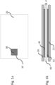
- Figure 1 shows the basic structure of the capacitor according to the present invention.
- the manufacturing technique proposed herein uses the technology currently employed for creating flexible multilayer printed circuit boards and not applied to the production of a capacitor with parallel flat faces.
- the internal layers of the capacitor consist of a layer of dielectric material 40, on the opposite sides of which two layers of conductive material 30 and 32 are deposited.
- the layers of conductive material 30 and 32 may be made of copper or another conductive material, including high-conductivity silicon.
- the external covering layers 20 and 22 are glued onto two layers of conductive material 30 and 32.
- One condition which is necessary for obtaining a component compliant with the specifications in terms of tolerable voltage is that the gluing operation must be carried out by using techniques ensuring the elimination of any residual air (or gas of any nature) from the interspaces that may be created at the contact edges between the conductive layer 30 and 32 and the external layer 20 and 22.
- Such external layers 20 and 22 act as covers, i.e. protective layers against local discharge phenomena (corona effect) caused by the high electric field to which the component and the surrounding materials may be subject. These external layers 20 and 22 also act as protections against external electrochemical agents (humidity, dust) and make the final product mechanically stronger.
- the layers 20 and 22 can therefore be applied by using techniques such as hot pressing or vacuum gluing.
- the dimensions of the dielectric layer 40 must exceed the dimensions of the layers of conductive material 30 and 32, so as to limit the edge effects (local increase in the electric field) that might cause discharge phenomena between the edges of the two conductive surfaces.
- the thickness of the external layer is chosen in such a way as to be at least three times greater than the thickness of the dielectric layer.
- the material used for making the dielectric layer 40 must also have good properties in terms of losses, in relation to the variable electric field to which it is subjected.
- the loss characteristics are often expressed as a parameter called loss figure or dissipation factor "Df".
- ESR equivalent series resistance
- the equivalent series resistance parameter ESR should be as low as possible, in order to ensure a behaviour of the component that is as close as possible to that of an ideal capacitor, wherein resistive phenomena are totally absent.
- the material should conveniently have a loss figure Df ⁇ 0.002.
- the contiguous layers of dielectric material 40 and of conductive material 30 and 32 must be created by using techniques not requiring the use of any additional materials, i.e. such layers must be made to mechanically adhere to each other without using any kind of glue.
- the succession of conductive-dielectric-conductive layers can be created by using different techniques among those typically employed for creating film printed boards.
- Such techniques include, for example, photoresistive deposition, photoresistive removal, galvanic deposition and plasma enhanced chemical vapour deposition (PECVD).
- Gluing techniques are avoided because the presence of glues/resins would add a layer of material having dielectric properties poorly compatible with the application.
- the layer of glue/resin would have a higher loss figure Df and a lower dielectric strength than the materials suitable for the creation of the dielectric layer.
- the layer of glue/resin would imply increased losses and hence an increased ESR of the capacitor (approximately by a factor of 10 in comparison with the case with deposited conductive layer).
- Different materials can be used for making the dielectric layer 40, including, for example, different polyamide films, some of which are typically used in the production of printed circuit boards, and fluorinated ethylene propylene (FEP). It is essential that the materials used for making the dielectric layer 40, in addition to having the above-mentioned electric properties, also allow depositing the conductive material in the total absence of glues.
- FEP fluorinated ethylene propylene
- all those technologies including intermediate steps of depositing the dielectric material on the surface of the conductive material may be equally employed, i.e. any technology allowing the physical making of the succession of layers 30, 40 and 32 without interposition of any intermediate material, i.e. with physical-mechanical continuity between the layers.
- the external covering layers 20 and 22, or covers, of the capacitor must ensure protection of the conductive layers 30 and 32 against external agents and the absence of any discharge phenomenon, typically known as "corona" effect.
- the corona effect occurs because of a local increase in the electric field, which increase is related to the edge effects between the two conductive layers.
- the electric field gradient is such as to exceed the dielectric strength, e.g. of the air surrounding the component (approx. 3 kV/mm)
- the latter is ionized.
- Such ionization shows itself as a local discharge phenomenon at the edges of one or both the internal conductive layers. This discharge causes a quick deterioration of the external covering layers 20 and 22 and also of the dielectric layer 40, which will then break after only a few work cycles of the component, thus limiting the operating range of the latter in terms of voltage that can be tolerated by the component itself.
- the corona effect can be triggered on the outer side of the external layers 20 and 22 and also in any interspaces possibly created within the interface to the conductive layers 30 and 32. In both cases, since it brings about local discharge phenomena, ionization will damage the nearby layer of dielectric material 40, leading to a rapid deterioration of the capacitor.
- the external covering layers 20 and 22 must perfectly adhere to the layers of conductive material 30 and 32, so as to ensure the absence of residual air in any interspaces.
- the material used for the external covering layers, or covers, 20 and 22 must therefore ensure:
- the dielectric strength of the material used for the external covering layers 20 and 22 must therefore be equal to or greater than that of the material used for the dielectric layer 40.
- Another typical advantage of the capacitor made as described herein is the low value of self-inductance or parasitic inductance (ESL) of such elements.
- Said low self-inductance value is a direct consequence of the planar design of the object.
- film capacitors which, since they typically have cylindrical shapes, show increased self-chaining of the magnetic field generated by the flow of electric current, resulting in higher ESL.
- the connections of the conductive layers 30 and 32 are effected by means of areas or patches 10 and 12 formed on the external covering layers 20 and 22. On such patches, by using another conductive material (including high-conductivity silicon), it is possible to glue or solder connection elements to the external circuitry.
- patches are areas of the conductive layers 30 and 32 that are left uncovered by the external layer, or cover, 20 or 22. Therefore, a patch is a sort of mask created on the covering layer before it is glued onto the conductive layer.
- the maximum tolerable temperature or maximum operating temperature of the dielectric material 40 and of the external covering layers 20 and 22 must therefore ensure the condition Tw>200°C (typically Tw>300°C) to allow easy soldering of the connection points.
- connection points will have to be locally protected and insulated by means of suitable insulation systems to ensure the absence of the same phenomena already described with reference to the external covering layers 20 and 22.
- connections can be insulated by means of polyamide tapes and films, insulating lacquers, polyurethane-based foams, silicon-based gels and pastes, insulating sheaths, even in multiple layers and combinations thereof.
- Kapton tape on the connection pin and protect the connection itself with heat-shrink tubing.
- the precision in obtaining the desired capacity value is dictated by three main parameters:
- Manufacturing the multilayer capacitor by using the technology for the production of printed circuit boards allows attaining levels of precision on the surfaces which can compensate for the errors deriving from the tolerances on the other two parameters.
- the final error can be reduced to values below 2% directly at the design stage.
- the invention applies to a field of application characterized by levels of frequency and voltage that no existing component can cover.
- the production cost of the capacitors built by using the proposed technique can be reduced by a factor of approximately ten compared to mica capacitors.
- These latter components are, among existing components, those that cover the broadest range in terms of voltage and frequency.
- the tolerable voltage levels allow overcoming the limitations suffered by the existing technologies.
- the precision levels that can be achieved in the production process allow obtaining an object that is particularly suited to resonant circuits, wherein system performance is improved by the insertion of the capacitor in terms of process effectiveness and efficiency of the electronic power converters at a given switching frequency.
- a further advantage is represented by the mechanical features of the usable materials.
- Such materials have very good characteristics in terms of strength and flexibility, especially in comparison with the characteristics of mica, which is notoriously a very fragile material.
- the thicknesses and areas obtained are advantageous in terms of cooling.
- the capacitors made by using the techniques proposed herein have very low thermal capacities and resistances. This allows for simpler heat removal by means of classical passive methods (heat sinks), avoiding the recourse to more complex liquid-cooling systems.
- multiple capacitors can be arranged in parallel by setting the individual patches 10 and 12 in front of each other and interposing the connection between the two external covering layers 20 and 22.
- connection point there is a connection point at a potential much higher than that of a second connection point.
- this voltage is equal to the output voltage of the power converter (typically ranging from hundreds of volts to one thousand volts, depending on the power of the system).
- connection point In applications with "series" compensation, one connection point will have a potential equal to the output voltage of the power converter, whereas a second point, connected to the inductor, will have a voltage ranging from hundreds to thousands of volts, depending on the power of the system.
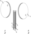
- FIGS 5a and 5b show a variant embodiment of the capacitor of Figure 1 , wherein said capacitor has a discoid shape.
- the layers that compose the capacitor are the same as those already described, the only difference being its shape, which is circular instead of rectangular.
- This embodiment is presented herein because it is particularly suitable for the creation of integrated coilcompensation capacitor objects in future inductive recharging systems, in which the magnetic structure of the coils is circular in shape.
- the proposed invention applies to all industrial applications that utilize resonant LC circuits, such as induction hardening, reheating, melting and welding operations, induction cooking, induction heating.
- the invention in question is particularly fit for all recent inductive/wireless high-power transmission technologies, e.g. applications for recharging electric vehicles, while it already presents itself as an essential component for industrial-scale development of current prototypes for mobile inductive recharging.
- the invention can be employed in all those systems which require power supply and control of highly inductive loads through the adoption of resonant converters.
- the recharge station (or the section of the recharge tract, for future mobile recharging applications) 200 is connected to the electric distribution network 202.
- the two coils, i.e. the transmitting coil 208 and the receiving coil 108, constitute two inductors mutually coupled through an air tract typically comprised between 10 and 30 cm.
- the transmitting coil 208 is powered by an electronic power converter 204 that supplies high-frequency current, thus creating an alternating magnetic field. This field is concatenated by the receiving coil 108, thus giving rise, through the electromagnetic induction phenomenon (Faraday's law), to transfer of electric energy. The electric current induced in the receiving coil 108 is then rectified by an AC/DC converter 104, which allows recharging and interfacing to the battery 102 installed aboard the vehicle 100.
- an electronic power converter 204 that supplies high-frequency current, thus creating an alternating magnetic field.
- This field is concatenated by the receiving coil 108, thus giving rise, through the electromagnetic induction phenomenon (Faraday's law), to transfer of electric energy.
- the electric current induced in the receiving coil 108 is then rectified by an AC/DC converter 104, which allows recharging and interfacing to the battery 102 installed aboard the vehicle 100.
- the presence of the long air tract implies a poor magnetic coupling between the two coils 108 and 208.
- the frequencies typically adopted range from ten to one hundred kilohertz.
- the very impedance of the coils 108 and 208 represents a strong limitation to power transfer.
- the capacitors 206 and 106, called compensation capacitors are resorted to, which, when connected to the inductors and selected in such a way as to have a single resonance frequency for the whole system, can compensate for the impedance of the inductors.
- the compensation effect which causes the system to become a resonant system, brings numerous benefits.
- the installation of the capacitor(s) 106 aboard the vehicle allows maximizing the power transfer.
- the capacitor(s) 206 connected to the transmitting coil 208 by compensating for reactive phenomena, allows reducing the nominal power of the DC/AC converter 204, which must supply a purely active power equal to the power transferred to the battery 102 except for any losses. From the power electronics viewpoint, operating in resonance conditions allows the adoption of so-called soft switching techniques, i.e. switching ideally occurring without any losses, with great benefits in terms of overall efficiency of the system.
Landscapes
- Engineering & Computer Science (AREA)
- Power Engineering (AREA)
- Microelectronics & Electronic Packaging (AREA)
- Manufacturing & Machinery (AREA)
- Ceramic Engineering (AREA)
- Chemical & Material Sciences (AREA)
- Inorganic Chemistry (AREA)
- Fixed Capacitors And Capacitor Manufacturing Machines (AREA)
Description
- The present invention relates to techniques for manufacturing capacitors, and in particular for manufacturing capacitors for resonant circuits in power applications.
- More in detail, the invention can be employed in all industrial applications that require the use of highly inductive loads made resonant by capacitive compensation.
- Some classic application examples include all processes related to heating, welding, hardening and melting by electromagnetic induction.
- One application that is naturally addressed by the invention concerns inductive recharging systems for electric vehicles/systems, whether moving or stationary, which require the use of compensation/resonance capacitors both for the transmitting coil installed on the ground and for the receiving coil installed aboard the vehicle/system.
- More in detail, the invention relates to a solution for manufacturing capacitors for medium-voltage, high-frequency and high-current industrial applications.
- Industrial applications that make use of resonant loads are characterized by the use of components having ohmic-inductive characteristics, typically called inductors, which are employed in order to create magnetic fields at frequencies ranging from tens to hundreds of kilohertz (kHz).
- In applications such as induction welding, hardening and reheating, a magnetic field is used as a means for transferring power towards a metallic object. The magnetic field hitting the object is created and suitably directed by means of an inductor (L).
- The high impedance value of the inductors at the high electric frequencies employed requires the use of compensation capacitors in order to be able to increase the power that can actually be transferred to the object. This compensation also increases the efficiency of the transfer from the source, which typically consists of an electronic power converter.
- In applications for inductive recharge of electric vehicles, the inductor consists of a coil, referred to as transmitting coil, installed on the ground or, more generally, externally to and at a distance from the vehicle, which coil is used in order to create a magnetic field.
- This magnetic field induces a voltage in a secondary coil, referred to as receiving coil, which is positioned aboard the vehicle.
- Through magnetic induction on the receiving coil, it is possible to transfer electric energy to the vehicle without the need for physical contact between the source, located outside the vehicle, and the vehicle itself.
- In inductive power transfer applications, both coils, i.e. the transmitting and receiving coils, are conveniently compensated by means of capacitors (C) connected in series and/or in parallel.
- This compensation increases the capacity of the power transfer from the source to the vehicle, while also allowing the use of power electronics switching techniques that provide reduced switching and conduction losses, thereby improving the power transfer efficiency.
- In all of the above-mentioned applications, the capacitors are chosen in such a way as to resonate with the inductor at a given frequency imposed by the power electronics supplying power to the system. The coil-capacitor system (LC) thus becomes a resonant system. Such frequency may be set to an exact value or remain variable, as is the case in most reheating and hardening applications. The typical distance between the primary coil (transmitting coil or inductor) and the receiving coil (receiving object or metal object) ranges between one centimeter and ten centimeters.
- Due to the distances involved, the magnetic coupling between the two parts of the system is less than 50%.
- In such coupling conditions, the resonance of the coil-capacitor system results in a considerable increase in the voltage across the terminals of these two elements.
- The voltage across the compensation capacitor may become extremely high, reaching values within the medium-voltage range (tens of kV).
- By way of example, when the capacitor is connected in series to the inductor, the voltage across the capacitor will have values typically comprised between ten and a hundred times the source voltage.
- The capacities of interest in the applications addressed by the invention range between a few nanofarads and hundreds of nanofarads.
- The different types of capacitors currently in use in such applications cannot always tolerate voltages higher than one or two kilovolts (kV).
- Therefore, in order to use capacitors among those currently available on the market, it is necessary to create banks of multiple capacitors connected in series and in parallel for the purpose of obtaining an object having the desired capacity value and capable of tolerating the voltage involved.
- The capacitors currently available on the market are bulky, massive and heavy. The thermal characteristics resulting from these physical features are such as to often require the use of liquid-cooling systems, leading to a more complex mechanical structure of the resonator.
- Typical currents ranging from tens to hundreds of amperes are not an important limitation for the capacitors taken into account.
- At present, the capacitors typically employed in the applications addressed by this invention are film capacitors (which utilize polyester or polypropylene as a dielectric material between the conductive layers) and mica capacitors.
- The voltage value tolerated by the capacitors is dependent on the frequency of the current flowing in the circuit in which they have been inserted. While for mica capacitors such voltage is stable up to hundreds of kilohertz, for film capacitors the tolerable voltage value is as low as a few hundreds of volts for frequencies higher than ten kilohertz.
- Such low tolerated voltage values require that capacitor batteries be resorted to, resulting in higher costs, greater dimensions, more complex connections and increased complexity of the heat sinking systems.
- On top of this, current capacitors are also characterized by low tolerance as concerns the capacity value. Typical tolerances are approx. 20%, but may be as low as 5% for particularly accurate or selectable implementations, which are even more costly.
- Prior art documents referring to capacitive elements comprising layered arrangements of a dielectric layer interposed between two layers of conductive material include
JPH02290008 JPS63137408 US3649892 . - The attainment of reliable capacity values, i.e. with low tolerance relative to the nominal value, allows the power electronics to operate at the optimal resonance points of the system, in compliance with the design specifications. This is advantageous in terms of maximization of the power transferred to the object hit by the magnetic field (inductive heating applications) or maximization of the power transferred to the receiving coil, especially in inductive power transfer applications aimed at ensuring interoperability of different transmitters and receivers calibrated on the same frequency.
- This benefit will affects the efficiency of the converter itself, which, by operating in known and stable resonance conditions, will work in conditions of minimized switching losses.
- A need is therefore felt for providing solutions capable of overcoming the above-mentioned limitations: precision, small dimensions, high tolerated voltage and low cost.
- The present invention provides a capacitive element according to claim 1, a method for manufacturing a capacitive element according to claim 9 and a multilayer printed circuit board according to claim 16. Embodiments of the invention are set forth with the appended dependent claims.
- The invention described herein adapts an existing technology, which is currently being used for the production of printed circuit boards, and applies it to the production of capacitors dedicated to high-power industrial applications that utilize LC resonators, i.e. all those systems that make use of an inductor L, the impedance of which is compensated for through resonance with a capacitive element C (whether consisting of a single component or multiple interconnected components).
- Some typical examples of fields of application of LC resonators are: induction welding and heating, induction annealing and hardening of metals, inductive/wireless transmission of power.
- The invention described herein allows the production of capacitors capable of tolerating voltages three or four times higher than those tolerated by the capacitors currently available on the market, with a precision in providing the rated capacity value of less than 2%.
- A capacitor built in accordance with the technique proposed herein can be subjected to voltages of the order of ten kV and currents of the order of ten ampere, at frequencies of tens/hundreds of kHz.
- The capacitors that can be obtained with this technique are extremely thin and have large surfaces, which is advantageous in terms of heat dissipation and space occupation.
- Finally, the use of the multilayer printed circuit board technology ensures a cost reduction of approx. 70% for a single component and approx. 90% compared with the total cost of the minimum number of components currently employed in the applications of interest.
- The invention presented herein allows overcoming the existing voltage limitations of the capacitors currently in use, avoiding the recourse to batteries of multiple capacitors connected in series and in parallel, thereby reducing the losses in the dielectric layers and offering smaller dimensions.
- Further features and advantages of the invention will be illustrated in the following detailed description, which is provided merely by way of non-limiting example with reference to the annexed drawings, wherein:
-
Figures 1a and 1b show the basic structure of the capacitor according to the present invention, -
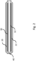
Figure 2 shows an example of embodiment of the capacitor according to the present invention, -
Figures 3a and 3b show, respectively, a top view and a bottom view of the capacitor according to the present invention, -
Figure 4 shows one possible example of a parallel connection of multiple capacitors, -
Figures 5a and 5b show, respectively, a top view and a bottom view of a variant of the capacitor according to the present invention, and -
Figure 6 shows one possible example of application of the capacitors according to the present invention. - The following description will illustrate various specific details useful for a deep understanding of some examples of one or more embodiments. The embodiments may be implemented without one or more of such specific details or with other methods, components, materials, etc. In other cases, some known structures, materials or operations will not be shown or described in detail in order to avoid overshadowing various aspects of the embodiments. Any reference to "an embodiment" in this description will indicate that a particular configuration, structure or feature is comprised in at least one embodiment. Therefore, the phrase "in an embodiment" and other similar phrases, which may be present in different parts of this description, will not necessarily be all related to the same embodiment. Furthermore, any particular configuration, structure or feature may be combined in one or more embodiments as deemed appropriate.
- The references below are therefore used only for simplicity's sake, and do not limit the protection scope or extension of the various embodiments.
- The invention makes use of a technology that is innovative in the field of power capacitor production. Such a construction technology allows obtaining high accuracy in the capacity value as well as using materials offering better performance in terms of dielectric strength (tolerated voltage) and efficiency. In the drawings, the proportions between the thicknesses of the different layers are strongly amplified for the sole purpose of making the drawings themselves clearer. The typical total thickness of all layers is less than one millimeter.
Figure 1 shows the basic structure of the capacitor according to the present invention. The manufacturing technique proposed herein uses the technology currently employed for creating flexible multilayer printed circuit boards and not applied to the production of a capacitor with parallel flat faces. - The internal layers of the capacitor consist of a layer of
dielectric material 40, on the opposite sides of which two layers ofconductive material - It is important to underline that between the layers of
conductive material dielectric layer 40 there is no other material or adhesive layer. The creation of the alternated conductive/dielectric layers therefore occurs by deposition, not by gluing. Of course, deposition of the conductive material may be effected starting from the dielectric material or vice versa, since both deposition procedures are possible. - By way of example, the layers of
conductive material conductive material conductive layer external layer - Such
external layers external layers - By way of example, the
layers - The capacity value obtained can be expressed with the classic formula for calculating the capacity between two parallel flat faces:

layer 40, "S" is the mutually facing area of the two layers of conductive material deposited on the sides of the dielectric layer, and "d" is the distance between them, i.e. the thickness of thedielectric material 40. - From this formula, one can deduce two fundamental characteristics for the materials that may be used for making the
dielectric layer 40, i.e.: - dielectric permittivity εr>1 (typically εr>2);
- extremely small thickness of the dielectric layer 40 (typically d<0.1mm). The thickness of the suitable material depends on its properties in terms of dielectric strength, i.e. the maximum electric field value tolerated by the material before it reaches the electric discharge. The materials used for the application must have a very high dielectric strength "k":
- dielectric strength k>100kV/mm (typically k>250kV/mm).
- The dimensions of the
dielectric layer 40 must exceed the dimensions of the layers ofconductive material - In several embodiments, the thickness of the external layer is chosen in such a way as to be at least three times greater than the thickness of the dielectric layer.
- The material used for making the
dielectric layer 40 must also have good properties in terms of losses, in relation to the variable electric field to which it is subjected. - The loss characteristics are often expressed as a parameter called loss figure or dissipation factor "Df".
- The losses in the capacitor give rise to an equivalent resistive behaviour expressed as a parameter called equivalent series resistance, designated as "ESR".
- The equivalent series resistance parameter ESR should be as low as possible, in order to ensure a behaviour of the component that is as close as possible to that of an ideal capacitor, wherein resistive phenomena are totally absent. The capacity values obtained, the equivalent series resistance "ESR" and the loss figure "Df" are bound to the frequency of the application according to the following expression:

- In the applications taken into account herein, the material should conveniently have a loss figure Df≤0.002.
- In order to ensure such a loss figure "Df", the contiguous layers of
dielectric material 40 and ofconductive material - In general, the succession of conductive-dielectric-conductive layers can be created by using different techniques among those typically employed for creating film printed boards. Such techniques include, for example, photoresistive deposition, photoresistive removal, galvanic deposition and plasma enhanced chemical vapour deposition (PECVD).
- Gluing techniques are avoided because the presence of glues/resins would add a layer of material having dielectric properties poorly compatible with the application. In particular, with reference to the characteristics of the materials typically used for creating multilayer circuits, the layer of glue/resin would have a higher loss figure Df and a lower dielectric strength than the materials suitable for the creation of the dielectric layer. As a main effect, the layer of glue/resin would imply increased losses and hence an increased ESR of the capacitor (approximately by a factor of 10 in comparison with the case with deposited conductive layer).
- Different materials can be used for making the
dielectric layer 40, including, for example, different polyamide films, some of which are typically used in the production of printed circuit boards, and fluorinated ethylene propylene (FEP). It is essential that the materials used for making thedielectric layer 40, in addition to having the above-mentioned electric properties, also allow depositing the conductive material in the total absence of glues. - As regards the creation of the internal layers, all those technologies including intermediate steps of depositing the dielectric material on the surface of the conductive material may be equally employed, i.e. any technology allowing the physical making of the succession of
layers - The external covering layers 20 and 22, or covers, of the capacitor must ensure protection of the
conductive layers - The corona effect occurs because of a local increase in the electric field, which increase is related to the edge effects between the two conductive layers. When the electric field gradient is such as to exceed the dielectric strength, e.g. of the air surrounding the component (approx. 3 kV/mm), the latter is ionized. Such ionization shows itself as a local discharge phenomenon at the edges of one or both the internal conductive layers. This discharge causes a quick deterioration of the external covering layers 20 and 22 and also of the
dielectric layer 40, which will then break after only a few work cycles of the component, thus limiting the operating range of the latter in terms of voltage that can be tolerated by the component itself. - The corona effect can be triggered on the outer side of the
external layers conductive layers dielectric material 40, leading to a rapid deterioration of the capacitor. - As shown in
Figure 2 , the external covering layers 20 and 22 must perfectly adhere to the layers ofconductive material - The material used for the external covering layers, or covers, 20 and 22 must therefore ensure:
- perfect adhesion to the
conductive layers dielectric layer 40; - a thickness that will prevent ionization of the air layers around the capacitor; and
- a dielectric strength that will prevent ionization of the same dielectric material they are made of.
- The dielectric strength of the material used for the external covering layers 20 and 22 must therefore be equal to or greater than that of the material used for the
dielectric layer 40. - Particular attention must be paid to eliminating any sharp corners (to be understood as angles having a size of less than 45°) of the conductive surfaces, so as to avoid any phenomena of charge accumulation at the apexes. Such accumulated charges may also lead to a considerable local electric field increase, resulting in collapse of the dielectric material.
- Thanks to the use of the technology for the production of printed circuit boards, this constraint can be complied with in an extremely accurate manner.
- It should also be added that the capacitor manufactured by using the process and materials described herein is flexible.
- Another typical advantage of the capacitor made as described herein is the low value of self-inductance or parasitic inductance (ESL) of such elements. Said low self-inductance value is a direct consequence of the planar design of the object. The same cannot be said, for example, for film capacitors, which, since they typically have cylindrical shapes, show increased self-chaining of the magnetic field generated by the flow of electric current, resulting in higher ESL.
- As shown in
Figures 1 and3 , the connections of theconductive layers patches - In particular, patches are areas of the
conductive layers - In welding applications, it is assumed that the materials adopted in the manufacturing technique presented herein can tolerate operating temperatures "Tw" of a few hundreds degrees centigrade.
- The maximum tolerable temperature or maximum operating temperature of the
dielectric material 40 and of the external covering layers 20 and 22 must therefore ensure the condition Tw>200°C (typically Tw>300°C) to allow easy soldering of the connection points. - The connection points will have to be locally protected and insulated by means of suitable insulation systems to ensure the absence of the same phenomena already described with reference to the external covering layers 20 and 22.
- In particular, the connections can be insulated by means of polyamide tapes and films, insulating lacquers, polyurethane-based foams, silicon-based gels and pastes, insulating sheaths, even in multiple layers and combinations thereof. By way of example, in various embodiments it is possible to apply Kapton tape on the connection pin and protect the connection itself with heat-shrink tubing. The precision in obtaining the desired capacity value is dictated by three main parameters:
- tolerance on the thickness "d" of the
dielectric layer 40; - tolerance on the dielectric permittivity "εr" of the material of the
dielectric layer 40, - tolerance on the alignment of the two mutually facing
conductive surfaces - Manufacturing the multilayer capacitor by using the technology for the production of printed circuit boards allows attaining levels of precision on the surfaces which can compensate for the errors deriving from the tolerances on the other two parameters. The final error can be reduced to values below 2% directly at the design stage.
- The invention presented herein proves to be innovative compared to the technologies currently available on the market.
- The invention applies to a field of application characterized by levels of frequency and voltage that no existing component can cover.
- Implementing the invention will allow reducing the cost, size and complexity of compensation/resonance systems.
- In particular, the production cost of the capacitors built by using the proposed technique can be reduced by a factor of approximately ten compared to mica capacitors. These latter components are, among existing components, those that cover the broadest range in terms of voltage and frequency.
- The tolerable voltage levels, according to the characteristics of the materials and the proposed production process, allow overcoming the limitations suffered by the existing technologies.
- The precision levels that can be achieved in the production process allow obtaining an object that is particularly suited to resonant circuits, wherein system performance is improved by the insertion of the capacitor in terms of process effectiveness and efficiency of the electronic power converters at a given switching frequency.
- A further advantage is represented by the mechanical features of the usable materials.
- Such materials have very good characteristics in terms of strength and flexibility, especially in comparison with the characteristics of mica, which is notoriously a very fragile material.
- The thicknesses and areas obtained are advantageous in terms of cooling. Unlike the capacitors currently in use, the capacitors made by using the techniques proposed herein have very low thermal capacities and resistances. This allows for simpler heat removal by means of classical passive methods (heat sinks), avoiding the recourse to more complex liquid-cooling systems. As shown in
Figure 4 , multiple capacitors can be arranged in parallel by setting theindividual patches - The parallel connection of multiple capacitors, obtained in accordance with the present recommendations, brings advantages in terms of electric safety. Such a spatial distribution of the components is characteristic of the manufactured object and cannot be found in any component currently available on the market. In
Figure 4 ,reference 50 indicates the high-potential connections, whereas 60 indicates the low-potential connections. - In various embodiments, there is a connection point at a potential much higher than that of a second connection point. In applications with "parallel" compensation, this voltage is equal to the output voltage of the power converter (typically ranging from hundreds of volts to one thousand volts, depending on the power of the system).
- In applications with "series" compensation, one connection point will have a potential equal to the output voltage of the power converter, whereas a second point, connected to the inductor, will have a voltage ranging from hundreds to thousands of volts, depending on the power of the system.
- In mixed compensation topologies (i.e. with a set of capacitors connected both in series and in parallel), voltages nevertheless remain at values comparable to the series and parallel topologies.
- The method of connection indicated herein allows protecting the connection at higher potential, making it inaccessible from the outside, resulting in protection against undesired phenomena of outward capacitive coupling and discharge.
Figures 5a and 5b show a variant embodiment of the capacitor ofFigure 1 , wherein said capacitor has a discoid shape. The layers that compose the capacitor are the same as those already described, the only difference being its shape, which is circular instead of rectangular. This embodiment is presented herein because it is particularly suitable for the creation of integrated coilcompensation capacitor objects in future inductive recharging systems, in which the magnetic structure of the coils is circular in shape. - The advantages mentioned below refer to the technologies used for manufacturing the capacitors currently available on the market and employed in applications for which the invention is proposed as an alternative. Performance comparisons are indicated as order of magnitude or range of values.
- Maximum (peak) voltage
- Currently: 1.4-2.8 kV
- Invention: >8 kV
- Equivalent series resistance ESR (@ 100 kHz)
- Currently: 0.35-1 Ω
- Invention: 0.25 Ω-0.5 Ω
- Relative precision of the capacity value
- Currently: 5-10%
- Invention: <2%
- Typical volume of the single component
- Currently: ~10^2 cm3
- Invention: ~10^-1 cm3
- Unitary cost of the component
- Currently: ∼100 € per ten nF
- Invention: ∼10 € per ten nF
- The proposed invention applies to all industrial applications that utilize resonant LC circuits, such as induction hardening, reheating, melting and welding operations, induction cooking, induction heating.
- The invention in question is particularly fit for all recent inductive/wireless high-power transmission technologies, e.g. applications for recharging electric vehicles, while it already presents itself as an essential component for industrial-scale development of current prototypes for mobile inductive recharging.
- Finally, the invention can be employed in all those systems which require power supply and control of highly inductive loads through the adoption of resonant converters.
- In the application naturally addressed by the invention, i.e. inductive recharging systems for electric vehicles, it is necessary to use compensation/resonance capacitors for the transmitting coil installed on the ground and for the receiving coil installed aboard the vehicle.
- With reference to
Figure 6 , the recharge station (or the section of the recharge tract, for future mobile recharging applications) 200 is connected to theelectric distribution network 202. The two coils, i.e. the transmittingcoil 208 and the receivingcoil 108, constitute two inductors mutually coupled through an air tract typically comprised between 10 and 30 cm. - The transmitting
coil 208 is powered by anelectronic power converter 204 that supplies high-frequency current, thus creating an alternating magnetic field. This field is concatenated by the receivingcoil 108, thus giving rise, through the electromagnetic induction phenomenon (Faraday's law), to transfer of electric energy. The electric current induced in the receivingcoil 108 is then rectified by an AC/DC converter 104, which allows recharging and interfacing to thebattery 102 installed aboard thevehicle 100. - The presence of the long air tract implies a poor magnetic coupling between the two
coils coils capacitors coil 208, by compensating for reactive phenomena, allows reducing the nominal power of the DC/AC converter 204, which must supply a purely active power equal to the power transferred to thebattery 102 except for any losses. From the power electronics viewpoint, operating in resonance conditions allows the adoption of so-called soft switching techniques, i.e. switching ideally occurring without any losses, with great benefits in terms of overall efficiency of the system. - Of course, without prejudice to the principle of the invention, the forms of embodiment and the implementation details may be extensively varied from those described and illustrated herein merely by way of non-limiting example, without however departing from the protection scope of the present invention as set out in the appended claims.
Claims (16)
- Capacitive element manufactured by using multilayer printed circuit board technology, wherein the body of the element comprises a layer of dielectric material (40) interposed between two layers of conductive material (30,32) arranged on opposite sides of said layer of dielectric material (40), wherein each layer of conductive material (30,32) is in turn covered, on its free side, with an external covering layer (20,22); the material for making said layer of dielectric material (40) is chosen among materials having:- a dielectric permittivity εr>1,- a dielectric strength k>100kV/mm, and- a dissipation factor Df≤0.002,and wherein the dimensions of said layer of dielectric material (40) are greater than the dimensions of said layers of conductive material (30,32), so as to limit the edge effects that might cause discharge phenomena, and wherein said layer of dielectric material (40) is chosen among a polyamide film, a fluorinated ethylene propylene (FEP) film and silicon oxide, and make said capacitive element flexible.
- Capacitive element according to claim 1, wherein said layer of dielectric material (40) is chosen among materials that allow depositing the conductive material for making said layers of conductive material (30,32) without requiring the use of glues.
- Capacitive element according to any one of the preceding claims, wherein said external covering layers (20,22) are hot pressed or vacuum glued to said layers of conductive material (30,32), so as to ensure that there will be no residual air in any interspaces, thus preventing local discharge phenomena.
- Capacitive element according to claim 3, wherein the material for said external covering layers (20,22) is chosen in such a way as to ensure:- perfect adhesion to the conductive layers (30,32) and to the dielectric layer (40);- a thickness that will prevent ionization of the air layers around the capacitive element; and- a dielectric strength that will prevent local discharge phenomena from arising, which might lead to perforation of the dielectric material.
- Capacitive element according to claim 4, wherein the dielectric strength of the material used for the external covering layers (20,22) is equal to or greater than the dielectric strength of the material used for the dielectric layer (40).
- Capacitive element according to claim 4, wherein the thickness of the material used for the external covering layers (20,22) is greater than or equal to the thickness of the material used for the dielectric layer (40).
- Capacitive element according to any one of the preceding claims, wherein the connections of the conductive layers (30,32) are effected by means of holes or patches (10,12) formed on said external covering layers (20,22), whereon electric connection elements can be glued or soldered.
- Capacitive element according to any one of the preceding claims, wherein the operating temperature Tw of the materials of the layer of dielectric material (40) and of the external covering layers (20,22) is Tw>200°C.
- Method for manufacturing a flexible capacitive element by multilayer printed circuit board technology, comprising the steps of:- preparing a layer of dielectric material (40),- forming two layers of conductive material (30,32) on opposite sides of said layer of dielectric material (40),- covering the free side of each layer of conductive material (30,32) with an external covering layer (20,22),- selecting the material for making said layer of dielectric material (40) among materials having:- a dielectric permittivity εr>1,- a dielectric strength k>100kV/mm, and- a dissipation factor Df≤0.002,and wherein said method comprises the steps of:- selecting the dimensions of said layer of dielectric material (40) in a manner such that they are greater than the dimensions of said layers of conductive material (30,32), so as to limit the edge effects that might cause discharge phenomena,- selecting the material for making said layer of dielectric material (40) among a polyamide film and a fluorinated ethylene propylene (FEP) film and silicon oxide.
- Method according to claim 9, wherein said method comprises the step of selecting the material for making said layer of dielectric material (40) among materials that allow depositing the conductive material for making said layers of conductive material (30,32) without requiring the use of glues.
- Method according to any one of the preceding claims 9-10, wherein said method comprises the step of causing said external covering layers (20,22) to be hot pressed or vacuum glued to said layers of conductive material (30,32), so as to ensure that where will be no residual air in any interspaces, thus preventing local discharge phenomena.
- Method according to claim 11, wherein said method comprises the step of selecting the material for making said external covering layers (20,22) in such a way as to ensure:- perfect adhesion to the conductive layers (30,32) and to the dielectric layer (40);- a thickness that will prevent ionization of the air layers around the capacitive element; and- a dielectric strength that will prevent the dielectric material from collapsing.
- Method according to claim 12, wherein the dielectric strength of the material used for the external covering layers (20,22) is selected to be equal to or greater than the dielectric strength of the material used for the dielectric layer (40).
- Method according to any one of the preceding claims 9-13, wherein said method comprises the step of prearranging connections of the conductive layers (30,32) by forming areas or patches (10,12) on said external covering layers (20,22), whereon connection elements can be glued or soldered.
- Method according to any one of the preceding claims 9-14, wherein said method comprises the step of selecting the materials of said layer of dielectric material (40) and said external covering layers (20,22) among materials having an operating temperature Tw>200°C.
- Multilayer printed circuit board comprising a capacitive element manufactured by using the method according to any one of claims 9 to 15.
Applications Claiming Priority (2)
| Application Number | Priority Date | Filing Date | Title |
|---|---|---|---|
| IT102017000032290A IT201700032290A1 (en) | 2017-03-23 | 2017-03-23 | CAPACITORS FOR RESONATING CIRCUITS IN POWER APPLICATIONS |
| PCT/IB2018/051889 WO2018172949A1 (en) | 2017-03-23 | 2018-03-21 | Capacitor for resonant circuits in power applications |
Publications (2)
| Publication Number | Publication Date |
|---|---|
| EP3602585A1 EP3602585A1 (en) | 2020-02-05 |
| EP3602585B1 true EP3602585B1 (en) | 2023-08-30 |
Family
ID=59683673
Family Applications (1)
| Application Number | Title | Priority Date | Filing Date |
|---|---|---|---|
| EP18717427.1A Active EP3602585B1 (en) | 2017-03-23 | 2018-03-21 | Capacitor for resonant circuits in power applications |
Country Status (4)
| Country | Link |
|---|---|
| US (1) | US11101076B2 (en) |
| EP (1) | EP3602585B1 (en) |
| IT (1) | IT201700032290A1 (en) |
| WO (1) | WO2018172949A1 (en) |
Families Citing this family (1)
| Publication number | Priority date | Publication date | Assignee | Title |
|---|---|---|---|---|
| DE102024129236A1 (en) * | 2024-10-10 | 2026-04-16 | Brusa Elektronik Ag | WIRELESS SYSTEM WITH MULTI-LAYER CAPER AND METHOD FOR ITS MANUFACTURING |
Family Cites Families (10)
| Publication number | Priority date | Publication date | Assignee | Title |
|---|---|---|---|---|
| US3484664A (en) * | 1968-11-21 | 1969-12-16 | Hercules Inc | Electrical capacitors |
| US3649892A (en) * | 1970-07-13 | 1972-03-14 | Mallory & Co Inc P R | Capacitors utilizing bonded discrete polymeric film dielectrics |
| US4323948A (en) * | 1977-12-05 | 1982-04-06 | Westinghouse Electric Corp. | Capacitor structures with improved electrical stress capability |
| JPH0766896B2 (en) * | 1986-11-28 | 1995-07-19 | 松下電器産業株式会社 | Film capacitor |
| JPH02290008A (en) * | 1989-04-28 | 1990-11-29 | Marcon Electron Co Ltd | Metallized plastic film capacitor |
| US6114015A (en) * | 1998-10-13 | 2000-09-05 | Matsushita Electronic Materials, Inc. | Thin-laminate panels for capacitive printed-circuit boards and methods for making the same |
| US6207522B1 (en) * | 1998-11-23 | 2001-03-27 | Microcoating Technologies | Formation of thin film capacitors |
| US7288459B2 (en) * | 2005-03-31 | 2007-10-30 | Intel Corporation | Organic substrates with integral thin-film capacitors, methods of making same, and systems containing same |
| JP4817855B2 (en) * | 2006-01-27 | 2011-11-16 | 京セラ株式会社 | Capacitor built-in wiring board and manufacturing method thereof |
| JP2018110196A (en) * | 2017-01-05 | 2018-07-12 | 富士通株式会社 | Circuit board, circuit board manufacturing method, and electronic apparatus |
-
2017
- 2017-03-23 IT IT102017000032290A patent/IT201700032290A1/en unknown
-
2018
- 2018-03-21 WO PCT/IB2018/051889 patent/WO2018172949A1/en not_active Ceased
- 2018-03-21 EP EP18717427.1A patent/EP3602585B1/en active Active
- 2018-03-21 US US16/495,963 patent/US11101076B2/en active Active
Also Published As
| Publication number | Publication date |
|---|---|
| US11101076B2 (en) | 2021-08-24 |
| IT201700032290A1 (en) | 2018-09-23 |
| US20200143993A1 (en) | 2020-05-07 |
| EP3602585A1 (en) | 2020-02-05 |
| WO2018172949A1 (en) | 2018-09-27 |
Similar Documents
| Publication | Publication Date | Title |
|---|---|---|
| EP1915809B1 (en) | Auxiliary winding for improved performance of a planar inductive charging platform | |
| CN102792401B (en) | Wireless power transmission magnetic cell and power supply device | |
| CN104471832B (en) | Wireless power transmission device, wireless power transmission device, and power receiving device | |
| EP2546999B1 (en) | Wireless power transmitting device for wireless power communication system | |
| CN105576847B (en) | Power transmission device, the vehicle and Wireless power transmission system for being equipped with power transmission device | |
| EP3032550B1 (en) | Coil printed wiring board, power reception module, battery unit, and power reception communication module | |
| US8129653B2 (en) | Plasma supply device | |
| US20160072336A1 (en) | Power transmitter, power supply device, power consumption device, power supply system and method for producing power transmitter | |
| CN105576715A (en) | Power transmission device, vehicle equipped with power transmission device, and wireless power transmission system | |
| KR101878353B1 (en) | Wireless Power Transmitters and Wireless Charging Device having the Same | |
| Al-Saadi et al. | Capacitive Power Transfer for Wireless Batteries Charging. | |
| JP6667163B2 (en) | Power transmission device, vehicle equipped with power transmission device, and wireless power transmission system | |
| US11303153B2 (en) | Wireless charging pad and wireless charging apparatus | |
| Al-Saadi et al. | Comparison of spiral and square coil configurations in wireless power transfer system for contactless battery charging | |
| US20150372505A1 (en) | Power transmission device and power reception device | |
| US10291080B2 (en) | Electric power transmission device and wireless electric power transfer system | |
| US10186903B2 (en) | Electrical breakdown protection for a capacitive wireless powering system | |
| EP3602585B1 (en) | Capacitor for resonant circuits in power applications | |
| Côte et al. | Design and optimization of a self-resonant impedance matched coil for Wireless Power Transfer | |
| EP4135096B1 (en) | Battery apparatus and manufacturing method therefor | |
| WO2023276797A1 (en) | Switching power supply device | |
| Mohammad et al. | Capacitor Design for Self-Resonant Coils for Long-Distance Wireless Power Transfer System | |
| US20260074564A1 (en) | Power transmission coil unit | |
| US20250273994A1 (en) | Wireless charging receiving device | |
| Bezawada et al. | Analysis of Influence Factors on Power Delivery Capability and Efficiency in Capacitive-Coupled WPT |
Legal Events
| Date | Code | Title | Description |
|---|---|---|---|
| STAA | Information on the status of an ep patent application or granted ep patent |
Free format text: STATUS: UNKNOWN |
|
| STAA | Information on the status of an ep patent application or granted ep patent |
Free format text: STATUS: THE INTERNATIONAL PUBLICATION HAS BEEN MADE |
|
| PUAI | Public reference made under article 153(3) epc to a published international application that has entered the european phase |
Free format text: ORIGINAL CODE: 0009012 |
|
| STAA | Information on the status of an ep patent application or granted ep patent |
Free format text: STATUS: REQUEST FOR EXAMINATION WAS MADE |
|
| 17P | Request for examination filed |
Effective date: 20190923 |
|
| AK | Designated contracting states |
Kind code of ref document: A1 Designated state(s): AL AT BE BG CH CY CZ DE DK EE ES FI FR GB GR HR HU IE IS IT LI LT LU LV MC MK MT NL NO PL PT RO RS SE SI SK SM TR |
|
| AX | Request for extension of the european patent |
Extension state: BA ME |
|
| DAV | Request for validation of the european patent (deleted) | ||
| DAX | Request for extension of the european patent (deleted) | ||
| GRAP | Despatch of communication of intention to grant a patent |
Free format text: ORIGINAL CODE: EPIDOSNIGR1 |
|
| STAA | Information on the status of an ep patent application or granted ep patent |
Free format text: STATUS: GRANT OF PATENT IS INTENDED |
|
| RIC1 | Information provided on ipc code assigned before grant |
Ipc: H05K 3/46 20060101ALN20230224BHEP Ipc: H05K 1/16 20060101ALI20230224BHEP Ipc: H01G 4/224 20060101ALI20230224BHEP Ipc: H01G 4/18 20060101AFI20230224BHEP |
|
| RIC1 | Information provided on ipc code assigned before grant |
Ipc: H05K 3/46 20060101ALN20230313BHEP Ipc: H05K 1/16 20060101ALI20230313BHEP Ipc: H01G 4/224 20060101ALI20230313BHEP Ipc: H01G 4/18 20060101AFI20230313BHEP |
|
| INTG | Intention to grant announced |
Effective date: 20230330 |
|
| RIC1 | Information provided on ipc code assigned before grant |
Ipc: H05K 3/46 20060101ALN20230320BHEP Ipc: H05K 1/16 20060101ALI20230320BHEP Ipc: H01G 4/224 20060101ALI20230320BHEP Ipc: H01G 4/18 20060101AFI20230320BHEP |
|
| GRAS | Grant fee paid |
Free format text: ORIGINAL CODE: EPIDOSNIGR3 |
|
| GRAA | (expected) grant |
Free format text: ORIGINAL CODE: 0009210 |
|
| STAA | Information on the status of an ep patent application or granted ep patent |
Free format text: STATUS: THE PATENT HAS BEEN GRANTED |
|
| AK | Designated contracting states |
Kind code of ref document: B1 Designated state(s): AL AT BE BG CH CY CZ DE DK EE ES FI FR GB GR HR HU IE IS IT LI LT LU LV MC MK MT NL NO PL PT RO RS SE SI SK SM TR |
|
| REG | Reference to a national code |
Ref country code: GB Ref legal event code: FG4D |
|
| REG | Reference to a national code |
Ref country code: CH Ref legal event code: EP |
|
| REG | Reference to a national code |
Ref country code: DE Ref legal event code: R096 Ref document number: 602018056372 Country of ref document: DE |
|
| REG | Reference to a national code |
Ref country code: IE Ref legal event code: FG4D |
|
| P01 | Opt-out of the competence of the unified patent court (upc) registered |
Effective date: 20230929 |
|
| REG | Reference to a national code |
Ref country code: NO Ref legal event code: T2 Effective date: 20230830 |
|
| REG | Reference to a national code |
Ref country code: LT Ref legal event code: MG9D |
|
| REG | Reference to a national code |
Ref country code: NL Ref legal event code: MP Effective date: 20230830 |
|
| REG | Reference to a national code |
Ref country code: AT Ref legal event code: MK05 Ref document number: 1606515 Country of ref document: AT Kind code of ref document: T Effective date: 20230830 |
|
| PG25 | Lapsed in a contracting state [announced via postgrant information from national office to epo] |
Ref country code: GR Free format text: LAPSE BECAUSE OF FAILURE TO SUBMIT A TRANSLATION OF THE DESCRIPTION OR TO PAY THE FEE WITHIN THE PRESCRIBED TIME-LIMIT Effective date: 20231201 |
|
| PG25 | Lapsed in a contracting state [announced via postgrant information from national office to epo] |
Ref country code: IS Free format text: LAPSE BECAUSE OF FAILURE TO SUBMIT A TRANSLATION OF THE DESCRIPTION OR TO PAY THE FEE WITHIN THE PRESCRIBED TIME-LIMIT Effective date: 20231230 |
|
| PG25 | Lapsed in a contracting state [announced via postgrant information from national office to epo] |
Ref country code: SE Free format text: LAPSE BECAUSE OF FAILURE TO SUBMIT A TRANSLATION OF THE DESCRIPTION OR TO PAY THE FEE WITHIN THE PRESCRIBED TIME-LIMIT Effective date: 20230830 Ref country code: RS Free format text: LAPSE BECAUSE OF FAILURE TO SUBMIT A TRANSLATION OF THE DESCRIPTION OR TO PAY THE FEE WITHIN THE PRESCRIBED TIME-LIMIT Effective date: 20230830 Ref country code: LV Free format text: LAPSE BECAUSE OF FAILURE TO SUBMIT A TRANSLATION OF THE DESCRIPTION OR TO PAY THE FEE WITHIN THE PRESCRIBED TIME-LIMIT Effective date: 20230830 Ref country code: LT Free format text: LAPSE BECAUSE OF FAILURE TO SUBMIT A TRANSLATION OF THE DESCRIPTION OR TO PAY THE FEE WITHIN THE PRESCRIBED TIME-LIMIT Effective date: 20230830 Ref country code: IS Free format text: LAPSE BECAUSE OF FAILURE TO SUBMIT A TRANSLATION OF THE DESCRIPTION OR TO PAY THE FEE WITHIN THE PRESCRIBED TIME-LIMIT Effective date: 20231230 Ref country code: HR Free format text: LAPSE BECAUSE OF FAILURE TO SUBMIT A TRANSLATION OF THE DESCRIPTION OR TO PAY THE FEE WITHIN THE PRESCRIBED TIME-LIMIT Effective date: 20230830 Ref country code: GR Free format text: LAPSE BECAUSE OF FAILURE TO SUBMIT A TRANSLATION OF THE DESCRIPTION OR TO PAY THE FEE WITHIN THE PRESCRIBED TIME-LIMIT Effective date: 20231201 Ref country code: FI Free format text: LAPSE BECAUSE OF FAILURE TO SUBMIT A TRANSLATION OF THE DESCRIPTION OR TO PAY THE FEE WITHIN THE PRESCRIBED TIME-LIMIT Effective date: 20230830 Ref country code: AT Free format text: LAPSE BECAUSE OF FAILURE TO SUBMIT A TRANSLATION OF THE DESCRIPTION OR TO PAY THE FEE WITHIN THE PRESCRIBED TIME-LIMIT Effective date: 20230830 |
|
| PG25 | Lapsed in a contracting state [announced via postgrant information from national office to epo] |
Ref country code: PL Free format text: LAPSE BECAUSE OF FAILURE TO SUBMIT A TRANSLATION OF THE DESCRIPTION OR TO PAY THE FEE WITHIN THE PRESCRIBED TIME-LIMIT Effective date: 20230830 Ref country code: NL Free format text: LAPSE BECAUSE OF FAILURE TO SUBMIT A TRANSLATION OF THE DESCRIPTION OR TO PAY THE FEE WITHIN THE PRESCRIBED TIME-LIMIT Effective date: 20230830 |
|
| PG25 | Lapsed in a contracting state [announced via postgrant information from national office to epo] |
Ref country code: ES Free format text: LAPSE BECAUSE OF FAILURE TO SUBMIT A TRANSLATION OF THE DESCRIPTION OR TO PAY THE FEE WITHIN THE PRESCRIBED TIME-LIMIT Effective date: 20230830 |
|
| PG25 | Lapsed in a contracting state [announced via postgrant information from national office to epo] |
Ref country code: SM Free format text: LAPSE BECAUSE OF FAILURE TO SUBMIT A TRANSLATION OF THE DESCRIPTION OR TO PAY THE FEE WITHIN THE PRESCRIBED TIME-LIMIT Effective date: 20230830 Ref country code: RO Free format text: LAPSE BECAUSE OF FAILURE TO SUBMIT A TRANSLATION OF THE DESCRIPTION OR TO PAY THE FEE WITHIN THE PRESCRIBED TIME-LIMIT Effective date: 20230830 Ref country code: ES Free format text: LAPSE BECAUSE OF FAILURE TO SUBMIT A TRANSLATION OF THE DESCRIPTION OR TO PAY THE FEE WITHIN THE PRESCRIBED TIME-LIMIT Effective date: 20230830 Ref country code: EE Free format text: LAPSE BECAUSE OF FAILURE TO SUBMIT A TRANSLATION OF THE DESCRIPTION OR TO PAY THE FEE WITHIN THE PRESCRIBED TIME-LIMIT Effective date: 20230830 Ref country code: DK Free format text: LAPSE BECAUSE OF FAILURE TO SUBMIT A TRANSLATION OF THE DESCRIPTION OR TO PAY THE FEE WITHIN THE PRESCRIBED TIME-LIMIT Effective date: 20230830 Ref country code: CZ Free format text: LAPSE BECAUSE OF FAILURE TO SUBMIT A TRANSLATION OF THE DESCRIPTION OR TO PAY THE FEE WITHIN THE PRESCRIBED TIME-LIMIT Effective date: 20230830 Ref country code: SK Free format text: LAPSE BECAUSE OF FAILURE TO SUBMIT A TRANSLATION OF THE DESCRIPTION OR TO PAY THE FEE WITHIN THE PRESCRIBED TIME-LIMIT Effective date: 20230830 Ref country code: PT Free format text: LAPSE BECAUSE OF FAILURE TO SUBMIT A TRANSLATION OF THE DESCRIPTION OR TO PAY THE FEE WITHIN THE PRESCRIBED TIME-LIMIT Effective date: 20240102 |
|
| REG | Reference to a national code |
Ref country code: DE Ref legal event code: R097 Ref document number: 602018056372 Country of ref document: DE |
|
| PLBE | No opposition filed within time limit |
Free format text: ORIGINAL CODE: 0009261 |
|
| STAA | Information on the status of an ep patent application or granted ep patent |
Free format text: STATUS: NO OPPOSITION FILED WITHIN TIME LIMIT |
|
| PG25 | Lapsed in a contracting state [announced via postgrant information from national office to epo] |
Ref country code: SI Free format text: LAPSE BECAUSE OF FAILURE TO SUBMIT A TRANSLATION OF THE DESCRIPTION OR TO PAY THE FEE WITHIN THE PRESCRIBED TIME-LIMIT Effective date: 20230830 |
|
| 26N | No opposition filed |
Effective date: 20240603 |
|
| REG | Reference to a national code |
Ref country code: SE Ref legal event code: RE72 Effective date: 20240722 Ref country code: SE Ref legal event code: TRGR |
|
| REG | Reference to a national code |
Ref country code: CH Ref legal event code: PL |
|
| PG25 | Lapsed in a contracting state [announced via postgrant information from national office to epo] |
Ref country code: BG Free format text: LAPSE BECAUSE OF FAILURE TO SUBMIT A TRANSLATION OF THE DESCRIPTION OR TO PAY THE FEE WITHIN THE PRESCRIBED TIME-LIMIT Effective date: 20230830 |
|
| PG25 | Lapsed in a contracting state [announced via postgrant information from national office to epo] |
Ref country code: LU Free format text: LAPSE BECAUSE OF NON-PAYMENT OF DUE FEES Effective date: 20240321 |
|
| PG25 | Lapsed in a contracting state [announced via postgrant information from national office to epo] |
Ref country code: MC Free format text: LAPSE BECAUSE OF FAILURE TO SUBMIT A TRANSLATION OF THE DESCRIPTION OR TO PAY THE FEE WITHIN THE PRESCRIBED TIME-LIMIT Effective date: 20230830 |
|
| GBPC | Gb: european patent ceased through non-payment of renewal fee |
Effective date: 20240321 |
|
| PG25 | Lapsed in a contracting state [announced via postgrant information from national office to epo] |
Ref country code: MC Free format text: LAPSE BECAUSE OF FAILURE TO SUBMIT A TRANSLATION OF THE DESCRIPTION OR TO PAY THE FEE WITHIN THE PRESCRIBED TIME-LIMIT Effective date: 20230830 Ref country code: LU Free format text: LAPSE BECAUSE OF NON-PAYMENT OF DUE FEES Effective date: 20240321 Ref country code: BG Free format text: LAPSE BECAUSE OF FAILURE TO SUBMIT A TRANSLATION OF THE DESCRIPTION OR TO PAY THE FEE WITHIN THE PRESCRIBED TIME-LIMIT Effective date: 20230830 |
|
| REG | Reference to a national code |
Ref country code: BE Ref legal event code: MM Effective date: 20240331 |
|
| PG25 | Lapsed in a contracting state [announced via postgrant information from national office to epo] |
Ref country code: BE Free format text: LAPSE BECAUSE OF NON-PAYMENT OF DUE FEES Effective date: 20240331 |
|
| PG25 | Lapsed in a contracting state [announced via postgrant information from national office to epo] |
Ref country code: GB Free format text: LAPSE BECAUSE OF NON-PAYMENT OF DUE FEES Effective date: 20240321 |
|
| PG25 | Lapsed in a contracting state [announced via postgrant information from national office to epo] |
Ref country code: IE Free format text: LAPSE BECAUSE OF NON-PAYMENT OF DUE FEES Effective date: 20240321 |
|
| PG25 | Lapsed in a contracting state [announced via postgrant information from national office to epo] |
Ref country code: IE Free format text: LAPSE BECAUSE OF NON-PAYMENT OF DUE FEES Effective date: 20240321 Ref country code: GB Free format text: LAPSE BECAUSE OF NON-PAYMENT OF DUE FEES Effective date: 20240321 Ref country code: BE Free format text: LAPSE BECAUSE OF NON-PAYMENT OF DUE FEES Effective date: 20240331 Ref country code: CH Free format text: LAPSE BECAUSE OF NON-PAYMENT OF DUE FEES Effective date: 20240331 |
|
| PG25 | Lapsed in a contracting state [announced via postgrant information from national office to epo] |
Ref country code: CY Free format text: LAPSE BECAUSE OF FAILURE TO SUBMIT A TRANSLATION OF THE DESCRIPTION OR TO PAY THE FEE WITHIN THE PRESCRIBED TIME-LIMIT; INVALID AB INITIO Effective date: 20180321 |
|
| PG25 | Lapsed in a contracting state [announced via postgrant information from national office to epo] |
Ref country code: HU Free format text: LAPSE BECAUSE OF FAILURE TO SUBMIT A TRANSLATION OF THE DESCRIPTION OR TO PAY THE FEE WITHIN THE PRESCRIBED TIME-LIMIT; INVALID AB INITIO Effective date: 20180321 |
|
| PG25 | Lapsed in a contracting state [announced via postgrant information from national office to epo] |
Ref country code: TR Free format text: LAPSE BECAUSE OF FAILURE TO SUBMIT A TRANSLATION OF THE DESCRIPTION OR TO PAY THE FEE WITHIN THE PRESCRIBED TIME-LIMIT Effective date: 20230830 |
|
| PGFP | Annual fee paid to national office [announced via postgrant information from national office to epo] |
Ref country code: SE Payment date: 20260323 Year of fee payment: 9 |
|
| PGFP | Annual fee paid to national office [announced via postgrant information from national office to epo] |
Ref country code: NO Payment date: 20260318 Year of fee payment: 9 Ref country code: DE Payment date: 20260320 Year of fee payment: 9 |
|
| PGFP | Annual fee paid to national office [announced via postgrant information from national office to epo] |
Ref country code: IT Payment date: 20260320 Year of fee payment: 9 |
|
| PGFP | Annual fee paid to national office [announced via postgrant information from national office to epo] |
Ref country code: FR Payment date: 20260323 Year of fee payment: 9 |