EP3599802B1 - Elektronische vorrichtung mit einem in einen schutzmantel eingebettetes bauteil - Google Patents
Elektronische vorrichtung mit einem in einen schutzmantel eingebettetes bauteil Download PDFInfo
- Publication number
- EP3599802B1 EP3599802B1 EP19187263.9A EP19187263A EP3599802B1 EP 3599802 B1 EP3599802 B1 EP 3599802B1 EP 19187263 A EP19187263 A EP 19187263A EP 3599802 B1 EP3599802 B1 EP 3599802B1
- Authority
- EP
- European Patent Office
- Prior art keywords
- container
- electrolytic capacitor
- compound
- circuit carrier
- potting compound
- Prior art date
- Legal status (The legal status is an assumption and is not a legal conclusion. Google has not performed a legal analysis and makes no representation as to the accuracy of the status listed.)
- Active
Links
Images

Classifications
-
- H—ELECTRICITY
- H05—ELECTRIC TECHNIQUES NOT OTHERWISE PROVIDED FOR
- H05K—PRINTED CIRCUITS; CASINGS OR CONSTRUCTIONAL DETAILS OF ELECTRIC APPARATUS; MANUFACTURE OF ASSEMBLAGES OF ELECTRICAL COMPONENTS
- H05K5/00—Casings, cabinets or drawers for electric apparatus
- H05K5/0026—Casings, cabinets or drawers for electric apparatus provided with connectors and printed circuit boards [PCB], e.g. automotive electronic control units
- H05K5/0034—Casings, cabinets or drawers for electric apparatus provided with connectors and printed circuit boards [PCB], e.g. automotive electronic control units having an overmolded housing covering the PCB
-
- H—ELECTRICITY
- H05—ELECTRIC TECHNIQUES NOT OTHERWISE PROVIDED FOR
- H05K—PRINTED CIRCUITS; CASINGS OR CONSTRUCTIONAL DETAILS OF ELECTRIC APPARATUS; MANUFACTURE OF ASSEMBLAGES OF ELECTRICAL COMPONENTS
- H05K5/00—Casings, cabinets or drawers for electric apparatus
- H05K5/0026—Casings, cabinets or drawers for electric apparatus provided with connectors and printed circuit boards [PCB], e.g. automotive electronic control units
- H05K5/0047—Casings, cabinets or drawers for electric apparatus provided with connectors and printed circuit boards [PCB], e.g. automotive electronic control units having a two-part housing enclosing a PCB
- H05K5/0056—Casings, cabinets or drawers for electric apparatus provided with connectors and printed circuit boards [PCB], e.g. automotive electronic control units having a two-part housing enclosing a PCB characterized by features for protecting electronic components against vibration and moisture, e.g. potting, holders for relatively large capacitors
Definitions
- the invention relates to an electronic device, in particular a control unit for a motor vehicle.
- the device has electrical components, including at least one circuit carrier, and a pressure-sensitive electronic component connected to the circuit carrier, in particular an electrolytic capacitor or a quartz oscillator. At least some of the components are each at least partially embedded in a molding compound, for example in documents DE 10 2008 043774 , DE 10 2016 204811 and DE 10 2010 002945 .
- the device according to claim 1 has a container with a container opening, the electrolytic capacitor being accommodated in the container.
- the container is filled with a particularly low-viscosity potting compound so that the electrolytic capacitor is enclosed by the potting compound, preferably embedded in the potting compound.
- the molding compound adjoins the container, in particular an outer wall of the container, and / or the potting compound in the area of the container opening in a materially and / or cohesively bonded manner.
- the casting compound thus forms a protective jacket for the electrolytic capacitor.
- the protective jacket is preferably produced in the container, the container being part of the device.
- the electrolytic capacitor cannot be damaged when the other electronic components are enveloped by the protective jacket formed in this way by the molding compound, which is injected into a tool mold, for example, under high pressure, in particular at at least 50 bar, preferably between 50 and 150 bar or be destroyed. This is because it has been recognized that the electrolytic capacitor can be damaged, in particular dented, during remolding by means of transfer molding, injection molding or by means of compression molding.
- the container is at least partially formed by a plastic part which encloses the capacitor.
- the plastic part is, for example, a pipe section.
- the pipe section can advantageously be placed on the circuit carrier.
- the pipe section is preferably designed to seal against the circuit carrier.
- the container can advantageously be filled with the low-viscosity potting compound, in particular epoxy resin, so that the capacitor, which is accommodated in the container, can be encased by the low-viscosity potting compound and thus embedded.
- an end section of the circuit carrier to which the electrolytic capacitor is connected is arranged together with the electrolytic capacitor in the container.
- the end section can, for example, be introduced into the container together with the electrolytic capacitor.
- the container can then be filled with the low-viscosity potting compound, the end section of the circuit carrier and the electrolytic capacitor being covered with potting compound.
- the electrolytic capacitor is advantageously completely embedded in the potting compound so that the electrolytic capacitor cannot be damaged when it is subsequently remolded with a molding compound under high pressure, insofar as the then cured, low-viscosity potting compound forms a protective jacket for the electrolytic capacitor.
- a container wall of the container is formed by the circuit carrier, and the plastic part is sealed against the circuit carrier.
- the container can thus advantageously be provided at low cost.
- the device has a plug connection, the plug connection through a to the container molded part, in particular plastic part is formed.
- the electronic device can thus advantageously be provided at low cost.
- the plug connection has a plug wall through which electrical contacts connected to the circuit carrier are passed.
- the plug wall preferably forms a container wall of the container.
- the feedthroughs of the contacts through the low-viscosity potting compound, which protrude - in particular on the inside of the plug connection - and are led to the circuit carrier, can be fixed and additionally sealed against the plug wall in the area of the passage through the plug wall by means of the potting compound.
- the plug contacts can be connected to the circuit carrier, for example, by means of soldering or by means of a press-fit connection.
- the plug connections can, for example, protrude at an angle from the circuit carrier.
- the plug connection in particular the plastic part forming the plug connection, can then be pushed onto the plug contacts in a further step.
- a container wall molded onto the plug connection can enclose or accommodate the end section of the circuit carrier on which the electrolytic capacitor is arranged.
- the container formed in this way, which is formed by part of the plug connection can then be filled with the low-viscosity potting compound.
- the openings in the plug wall are preferably each conical so that the insertion of the plug-in contacts when the plug-in connection is pushed on can be facilitated.
- the plug-in contacts can be encapsulated by the plug-in connection, in particular the plastic part forming the plug-in connection.
- the potting compound is formed by a resin, in particular epoxy resin.
- the casting compound can thus be inexpensive be provided as a low-viscosity casting compound.
- the potting compound is, for example, filled with particles, in particular filled with ceramic particles. The potting compound can thus advantageously dissipate heat losses generated by the electrolytic capacitor to the plug connection.
- the molding compound is formed by an injection molding compound that is in particular filled with particles.
- the particles are, for example, ceramic particles.
- a degree of filling in particular a proportion by volume or weight of the filler particles in the low-viscosity potting compound, is preferably less than the filler particle proportion in the molding compound, preferably less than half, more preferably less than a quarter of the filler particle proportion in the molding compound.
- the particles are preferably ceramic particles, in particular aluminum oxide particles, nitride particles, in particular boron nitride particles, or carbide particles, in particular silicon carbide particles or silicon oxide particles.
- the BMC compound preferably comprises polyester and / or vinyl ester resin.
- the molding compound is preferably formed by a reaction resin, in particular polycarbonate or a particle-filled epoxy resin.
- the potting compound is different from the molding compound.
- the potting compound is formed by an epoxy resin and the molding compound is formed by a phenolic resin.
- the invention also relates to a method according to claim 10 for producing an electronic device, in particular the device of the type described above.
- a pressure-sensitive electronic component such as an electrolytic capacitor or a quartz crystal, is electrically and mechanically connected to a circuit carrier.
- the component is enclosed with a container so that the component is received in the container.
- the container is filled with a particularly low-viscosity potting compound - in particular without excess pressure - preferably in a vacuum and / or by means of pure gravity, for example Pouring - filled so that the component is enclosed by the potting compound, preferably embedded in the potting compound.
- the component is encapsulated with an injection molding compound, the injection molding compound joining the potting compound and / or the container. The potting compound and the molding compound can thus advantageously contact one another.
- a cohesive or materially bonded boundary layer is preferably formed between the molding compound and the potting compound.
- the filling of the low-viscosity casting compound is preferably carried out in a vacuum. In this way, voids in the potting compound can advantageously be avoided. More preferably, the filling takes place in such a way that no increased pressure acts on the condenser compared to normal ambient air pressure or that damage to the condenser is excluded.
- An ambient air pressure is, for example, 1013 hectopascals.
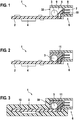
- FIG. 3 shows an exemplary embodiment for an electronic device 1 which is shown in FIG Figure 1 is partially shown.
- the electronic device 1 has a circuit carrier 2.
- an electrolytic capacitor 3 is electrically and mechanically connected to the circuit carrier 2.
- the circuit carrier 2 also has further electronic components, of which an integrated circuit 4 is designated as an example.
- the electronic device 1 forms a control device, in particular a control device for a motor vehicle.
- the electronic device 1 has a plug connector 6 for electrically connecting the electronic device 1 to a further electrical component, for example to a mating connector.
- the plug connection 6 comprises electrical contacts, of which one electrical contact 7 is designated as an example.
- the plug connection 6 has a plug-in collar 8 which encloses the electrical contacts, and thus also the electrical contact 7.
- the plug connection 6 has a cup wall 9 which is integrally formed on the plug connection 6 and which, in this embodiment, extends parallel to the flat extension of the circuit carrier 2.
- the plug connection 6 has a plug wall 10 through which the at least one electrical contact 7 is passed.
- the electrical contact 7 is electrically connected to the circuit carrier 2, in particular soldered.
- the plug connection 6 seals against the end section of the circuit carrier 2 so that - as in FIG Figure 2 shown - the cavity 5 - in particular the cavity remaining between the electrolytic capacitor 3 and the container walls of the container - can be filled with a low-viscosity potting compound 11 through an opening 32.
- FIG 2 are the in Figure 1 Parts of the electronic device 1 already shown are shown, the cavity 5 being filled with the potting compound 11, so that the capacitor 3 is enclosed by the potting compound 11 and thus - in particular completely - is embedded in the potting compound 11.
- the electrical contact 7 is also embedded in the potting compound 11 on a longitudinal section which extends between the plug wall 10 and the circuit carrier 2.
- Figure 3 shows a further step for generating the electronic device 1, in which the electronic device 1, in particular the electrical components, comprising the circuit carrier 2 and the electronic components connected to the circuit carrier 2, for example the integrated circuit 4, are surrounded by an injection molding compound 12, and so is embedded in the injection molding compound 12.
- the injection molding compound 12 adjoins the potting compound 11, so that a boundary layer 30 is formed between the potting compound 11 and the molding compound 12.
- the molding compound 12 is produced by means of a transfer molding method under overpressure, for example with at least 50 bar.
- the electronic device, including the circuit carrier 2 and the plug connection 6 is enclosed in two mold halves which, after being closed, can be filled with the molding compound under high filling pressure. After the mold halves have been opened, the circuit carrier 2 and the electronic components connected to the circuit carrier 2 are enclosed by the molding compound.
- the molding compound connects to the plug connection 6 and thus covers part of the plug connection 6.
- the potting compound 11 forms one for the electrolytic capacitor 3, which is sufficiently pressure-resistant so that the electrolytic capacitor 3 is affected by the pressure , in particular overpressure when remolding the circuit board 2 cannot be damaged.
- FIG. 4 shows an exemplary embodiment for an electronic device 40 in a sectional illustration.
- the electronic device 40 forms a variant of that shown in FIGS Figures 1, 2 and 3 1.
- the electronic device 40 has a circuit carrier 2 to which electronic components are connected, of which an integrated circuit 31 is designated by way of example.
- the device 40 comprises a plug connector 15.
- the plug connector 15 is designed in one piece as a plastic part.
- the plug connection 15 comprises a plug wall 18, through which electrical contacts are passed, and one end section protruding from the plug wall 18.
- One contact 19 of the electrical contacts is designated as an example.
- the end section 20 of the circuit carrier is received in a cup molded onto the plug connection 15, comprising a cup wall 16 and a cup wall 17, which each extend parallel to one another.
- the cup walls 16 and 17 are each molded onto the plug wall 18, the plug wall 18 forming a cup base on which the cup walls 16 and 17 are molded.
- the cup walls 16 and 17 together with the cup base formed by the plug wall 18 form a U-shape.
- a plug-in collar is formed on the cup base 18, which collar encloses the electrical contacts, and thus also the electrical contact 19.
- the electronic device 40 also has at least one electrolytic capacitor, in this exemplary embodiment an electrolytic capacitor 13, and an electrolytic capacitor 14, which are each connected to the circuit carrier 2 on opposite sides of the circuit carrier 2 on the end section 20.
- the electrolytic capacitors 13 and 14 are thus received together with the end section 20 of the circuit carrier 2 in the cup molded onto the plug connection 15, formed by the cup walls 16 and 17, and by the plug wall 18.
- the cavity remaining between the end section 20 of the circuit carrier and the electrolytic capacitors and the cup walls is filled with low-viscosity potting compound 11 in this exemplary embodiment.
- the remaining part of the circuit carrier, which protrudes from the plug connection 15, in particular from the cup molded onto the plug connection 15, is encapsulated with molding compound 12.
- a boundary layer 33 is formed between the molding compound 12 and the potting compound 11.
- the electrolytic capacitors 13 and 14 are thus protected during remolding by the protective jacket formed by the hardened potting compound 11 and can thus not be damaged by the pressure when the molding compound 12 is shot and hardened in a tool mold.
- FIG. 5 shows an exemplary embodiment for an electronic device 21.
- the electronic device 21 comprises a circuit carrier 22 to which electronic components are connected, of which an integrated circuit 29 is designated by way of example.
- An electrolytic capacitor 23 which in this exemplary embodiment forms a pressure-sensitive component, is also electrically and mechanically connected to the circuit carrier 22.
- the electrolytic capacitor 23 is enclosed in a cavity enclosed by a pipe section 24.
- the pipe section 24 has been slipped over the electrolytic capacitor 23 and thus placed on the circuit carrier 22.
- the pipe section 24 can thus be filled with low-viscosity potting compound 25 in a subsequent step.
- the circuit carrier 22 forms a cup base
- the pipe section 24 forms a cup wall.
- the circuit carrier 22, to which electrical connections 27 and 28 in this exemplary embodiment, can be connected are encased in a two-part mold with a molding compound 26, and thus embedded in the molding compound 26.
- the electrical connections 27 and 28 each protrude with an end section - in particular at an interface between the two tool halves - from a mold body formed after the molding compound 26 has hardened.
- the potting compound 25 is covered by the molding compound 26, so that a boundary layer 34 is formed between the potting compound 25 and the molding compound 26.
Landscapes
- Engineering & Computer Science (AREA)
- Microelectronics & Electronic Packaging (AREA)
- Structures Or Materials For Encapsulating Or Coating Semiconductor Devices Or Solid State Devices (AREA)
- Non-Metallic Protective Coatings For Printed Circuits (AREA)
Description
- Die Erfindung betrifft eine elektronische Vorrichtung, insbesondere ein Steuergerät für ein Kraftfahrzeug. Die Vorrichtung weist elektrische Komponenten, umfassend wenigstens einen Schaltungsträger, und einen mit dem Schaltungsträger verbundenes druckempfindliches elektronisches Bauteil, insbesondere einen Elektrolytkondensator oder einen Schwingquarz auf. Wenigstens ein Teil der Komponenten sind jeweils wenigstens teilweise in eine Mold-Masse eingebettet, wie zum Beispiel in Dokumenten
DE 10 2008 043774 ,DE 10 2016 204811 undDE 10 2010 002945 . - Erfindungsgemäß weist die Vorrichtung nach Anspruch 1 einen Behälter mit einer Behälteröffnung auf, wobei der Elektrolytkondensator in dem Behälter aufgenommen ist. Der Behälter ist mit einer insbesondere niedrigviskosen Vergussmasse gefüllt, sodass der Elektrolytkondensator von der Vergussmasse umschlossen, bevorzugt in die Vergussmasse eingebettet, ist. Die Mold-Masse schließt an den Behälter, insbesondere an eine Behälteraußenwand des Behälters, und/oder die Vergussmasse im Bereich der Behälteröffnung materialschlüssig und/oder stoffschlüssig an.
- Ausserdem bildet die Vergussmasse so einen Schutzmantel für den Elektrolytkondensator. Der Schutzmantel ist bevorzugt in dem Behälter erzeugt, wobei der Behälter Bestandteil der Vorrichtung ist. Vorteilhaft kann der Elektrolytkondensator durch den so gebildeten Schutzmantel von der Mold-Masse, welche beispielsweise unter Hochdruck, insbesondere bei wenigstens 50 Bar, bevorzugt zwischen 50 und 150 bar, in eine Werkzeugform eingeschossen wird, beim Umhüllen der übrigen elektronischen Komponenten nicht beschädigt oder zerstört werden. Es wurde nämlich erkannt, dass der Elektrolytkondensator beim Ummolden mittels Transfermolden, Spritzgießen oder mittels Compression Molding beschädigt, insbesondere eingedrückt werden kann.
- In einer bevorzugten Ausführungsform ist der Behälter wenigstens teilweise durch ein Kunststoffteil gebildet, welches den Kondensator umschließt. Das Kunststoffteil ist beispielsweise ein Rohrabschnitt. Der Rohrabschnitt kann vorteilhaft auf den Schaltungsträger gestellt werden. Der Rohrabschnitt ist bevorzugt ausgebildet, gegen den Schaltungsträger abzudichten. Vorteilhaft kann der Behälter so mit der niedrigviskosen Vergussmasse, insbesondere Epoxidharz, gefüllt werden, sodass der Kondensator, welcher in dem Behälter aufgenommen ist, von der niedrigviskosen Vergussmasse umhüllt, und so eingebettet sein kann.
- In einer anderen Ausführungsform ist ein Endabschnitt des Schaltungsträgers, mit dem der Elektrolytkondensator verbunden ist, gemeinsam mit dem Elektrolytkondensator in dem Behälter angeordnet. Der Endabschnitt kann beispielsweise zusammen mit dem Elektrolytkondensator in den Behälter eingeführt werden. Anschließend kann der Behälter mit der niedrigviskosen Vergussmasse gefüllt werden, wobei der Endabschnitt des Schaltungsträgers und der Elektrolytkondensator dabei mit Vergussmasse bedeckt werden. Vorteilhaft ist der Elektrolytkondensator so vollständig in die Vergussmasse eingebettet, sodass bei einem anschließenden Ummolden mit einer Mold-Masse unter Hochdruck der Elektrolytkondensator nicht beschädigt werden kann, insoweit die dann ausgehärtete niedrigviskose Vergussmasse einen Schutzmantel für den Elektrolytkondensator bildet.
- In einer bevorzugten Ausführungsform ist eine Behälterwand des Behälters durch den Schaltungsträger gebildet, und das Kunststoffteil ist gegen den Schaltungsträger abgedichtet. Vorteilhaft kann der Behälter so aufwandsgünstig bereitgestellt werden.
- In einer bevorzugten Ausführungsform weist die Vorrichtung einen Steckanschluss auf, wobei der Steckanschluss durch ein an den Behälter angeformtes Teil, insbesondere Kunststoffteil gebildet ist. Vorteilhaft kann die elektronische Vorrichtung so aufwandsgünstig bereitgestellt werden.
- In einer bevorzugten Ausführungsform weist der Steckanschluss eine Steckerwand auf, durch die mit dem Schaltungsträger verbundene elektrische Kontakte hindurchgeführt sind. Die Steckerwand bildet bevorzugt eine Behälterwand des Behälters. Vorteilhaft können so die Durchführungen der Kontakte durch die niedrigviskose Vergussmasse, die - insbesondere an einer Innenseite des Steckanschlusses - herausragen und zu dem Schaltungsträger hingeführt sind, im Bereich des Durchtritts durch die Steckerwand mittels der Vergussmasse gegen die Steckerwand fixiert und zusätzlich abgedichtet sein.
- Zum Erzeugen der Vorrichtung können die Steckkontakte beispielsweise mit dem Schaltungsträger mittels Löten oder mittels einer Einpressverbindung verbunden sein. Die Steckanschlüsse können beispielsweise abgewinkelt von dem Schaltungsträger wegragen. Der Steckanschluss, insbesondere das den Steckanschluss bildende Kunststoffteil, kann dann in einem weiteren Schritt auf die Steckkontakte aufgeschoben werden. Eine an den Steckanschluss angeformte Behälterwand kann dabei den Endabschnitt des Schaltungsträgers, auf dem der Elektrolytkondensator angeordnet ist, umschließen oder aufnehmen. Der so gebildete Behälter, welcher durch einen Teil des Steckanschlusses gebildet ist, kann dann mit der niedrigviskosen Vergussmasse gefüllt werden.
- Bevorzugt sind die Durchbrüche in der Steckerwand jeweils konisch ausgebildet, sodass ein Einführen der Steckkontakte beim Aufschieben des Steckanschlusses erleichtert werden kann.
- Die Steckkontakte können in einer anderen Ausführungsform von dem Steckanschluss, insbesondere dem den Steckanschluss bildenden Kunststoffteil umspritzt sein. Die Steckkontakte können so - beispielsweise abgewinkelt - mittels THT-Technologie (THT = Through-Hole-Technology) mit dem Schaltungsträger verbunden und verlötet werden.
- In einer bevorzugten Ausführungsform ist die Vergussmasse durch ein Harz, insbesondere Epoxidharz, gebildet. Die Vergussmasse kann so aufwandsgünstig als niedrigviskose Vergussmasse bereitgestellt werden. Die Vergussmasse ist beispielsweise partikelgefüllt, insbesondere mit Keramikpartikeln gefüllt. Die Vergussmasse kann so vorteilhaft von dem Elektrolytkondensator erzeugte Verlustwärme gut an den Steckanschluss ableiten.
- In einer bevorzugten Ausführungsform ist die Mold-Masse durch eine insbesondere partikelgefüllte Spritzgussmasse gebildet. Die Partikel sind beispielsweise Keramikpartikel.
- Bevorzugt beträgt ein Füllgrad, insbesondere ein Volumen- oder Gewichtsanteil der Füllpartikel in der niedrigviskosen Vergussmasse, weniger als der Füllpartikelanteil in der Mold-Masse, bevorzugt weniger als die Hälfte, weiter bevorzugt weniger als ein Viertel des Füllpartikelanteils in der Mold-Masse. Die Partikel sind bevorzugt Keramikpartikel, insbesondere Aluminiumoxidpartikel, Nitridpartikel, insbesondere Bornitridpartikel, oder Karbidpartikel, insbesondere Siliziumkarbidpartikel oder Siliziumoxidpartikel.
- Die Mold-Masse ist bevorzugt durch einen Duroplast, insbesondere Phenolharz, Melaminharz, Methanalharz oder eine insbesondere partikelgefüllte BMC-Masse (BMC = Bulk-Molding-Compound) gebildet. Die BMC-Masse weist bevorzugt Polyester- und/oder Vinylesterharz auf.
- Bevorzugt ist die Moldmasse durch ein Reaktionsharz, insbesondere Polykarbonat oder ein partikelgefülltes Epoxidharz, gebildet. In einer bevorzugten Ausführungsform ist die Vergussmasse von der Mold-Masse verschieden. Beispielsweise ist die Vergussmasse durch ein Epoxidharz gebildet und die Mold-Masse durch ein Phenolharz gebildet. Die Erfindung betrifft auch ein Verfahren nach Anspruch 10 zum Erzeugen einer elektronischen Vorrichtung, insbesondere der Vorrichtung der vorbeschriebenen Art. Bei dem Verfahren wird ein druckempfindliches elektronisches Bauteil, wie zum Beispiel ein Elektrolytkondensator oder ein Schwingquarz, mit einem Schaltungsträger elektrisch und mechanisch verbunden. Das Bauteil wird in einem weiteren Schritt mit einem Behälter umschlossen, sodass das Bauteil in dem Behälter aufgenommen ist. In einem folgenden Schritt wird der Behälter mit einer insbesondere niedrigviskosen Vergussmasse - insbesondere überdrucklos - bevorzugt im Vakuum und/oder mittels bloßer Schwerkraft beispielsweise durch Eingießen - gefüllt, sodass das Bauteil von der Vergussmasse umschlossen, bevorzugt in die Vergussmasse eingebettet, ist. In einem weiteren Schritt wird das Bauteil mit einer Spritzgussmasse ummoldet, wobei die Spritzgussmasse an die Vergussmasse und/oder den Behälter anschließt. Die Vergussmasse und die Mold-Masse können so vorteilhaft einander kontaktieren. Bevorzugt ist zwischen der Mold-Masse und der Vergussmasse eine stoffschlüssige oder materialschlüssige Grenzschicht gebildet.
- Das Einfüllen der niedrigviskosen Vergussmasse erfolgt bevorzugt im Vakuum. Vorteilhaft können so Lunker in der Vergussmasse vermieden werden. Weiter bevorzugt erfolgt das Einfüllen derart, dass auf den Kondensator gegenüber einem normalen Umgebungsluftdruck kein erhöhter Druck wirkt oder dass eine Beschädigung des Kondensators ausgeschlossen ist. Ein Umgebungsluftdruck beträgt beispielsweise 1013 Hektopascal.
- Die Erfindung wird nun im Folgenden anhand von Figuren und weiteren Ausführungsbeispielen beschrieben. Weitere vorteilhafte Ausführungsvarianten ergeben sich aus den in den Figuren und in den abhängigen Ansprüchen beschriebenen Merkmalen.
-
Figur 1 zeigt - schematisch - ein Ausführungsbeispiel für eine elektronische Vorrichtung, bei der ein druckempfindliches Bauelement, insbesondere ein Elektrolytkondensator mit einem Schaltungsträger lötverbunden ist; -
Figur 2 zeigt die inFigur 1 dargestellte elektronische Vorrichtung bei der der Elektrolytkondensator in eine insbesondere niedrigviskose Vergussmasse eingeschlossen wird; -
Figur 3 zeigt die inFigur 2 dargestellte elektronische Vorrichtung bei der der Schaltungsträger und die übrigen elektronischen Komponenten mit einer Moldmasse umhüllt werden, wobei die Moldmasse an die Vergussmasse unter Ausbildung einer Grenzschicht zwischen den Massen anschließt; -
Figur 4 zeigt - schematisch - eine elektronische Vorrichtung, bei der auf zueinander gegenüberliegenden Seiten des Schaltungsträgers jeweils ein Elektrolytkondensator angeordnet und mit dem Schaltungsträger verbunden ist; -
Figur 5 zeigt - schematisch - ein Ausführungsbeispiel für eine elektronische Vorrichtung, bei der ein Elektrolytkondensator mit einem Rohrabschnitt von einer Moldmasse isoliert ist, wobei der in dem Rohrabschnitt verbleibende Hohlraum mit einer Vergussmasse gefüllt ist. -
Figur 1 zeigt ein Ausführungsbeispiel für eine elektronische Vorrichtung 1, welche inFigur 1 teilweise dargestellt ist. Die elektronische Vorrichtung 1 weist einen Schaltungsträger 2 auf. Mit dem Schaltungsträger 2 ist in diesem Ausführungsbeispiel ein Elektrolytkondensator 3 elektrisch und mechanisch verbunden. Der Schaltungsträger 2 weist noch weitere elektronische Komponenten auf, von denen ein integrierter Schaltkreis 4 beispielhaft bezeichnet ist. Die elektronische Vorrichtung 1 bildet in diesem Ausführungsbeispiel ein Steuergerät, insbesondere ein Steuergerät für ein Kraftfahrzeug. - Die elektronische Vorrichtung 1 weist in diesem Ausführungsbeispiel einen Steckanschluss 6 zum elektrischen Verbinden der elektronischen Vorrichtung 1 mit einer weiteren elektrischen Komponente, beispielsweise mit einem Gegenstecker, auf. Der Steckanschluss 6 umfasst in diesem Ausführungsbeispiel elektrische Kontakte, von denen ein elektrischer Kontakt 7 beispielhaft bezeichnet ist.
- Der Steckanschluss 6 weist in diesem Ausführungsbeispiel einen Steckkragen 8 auf, welcher die elektrischen Kontakte, und so auch den elektrischen Kontakt 7, umschließt. Der Steckanschluss 6 weist in diesem Ausführungsbeispiel eine an den Steckanschluss 6 angeformte Becherwand 9 auf, welche sich in diesem Ausführungsbeispiel parallel zur flachen Erstreckung des Schaltungsträgers 2 erstreckt. Der Steckanschluss 6 weist eine Steckerwand 10 auf, durch die der wenigstens eine elektrische Kontakt 7 hindurchgeführt ist. Der elektrische Kontakt 7 ist mit dem Schaltungsträger 2 elektrisch verbunden, insbesondere Lötverbunden.
- Der Steckanschluss 6, insbesondere die Steckerwand 10, und die an die Steckerwand 10 angeformte Behälterwand 9 umschließen gemeinsam mit einem Endabschnitt des Schaltungsträgers 2 einen Hohlraum 5, in dem der Elektrolytkondensator 3 aufgenommen ist. Der Steckanschluss 6 dichtet in diesem Ausführungsbeispiel gegen den Endabschnitt des Schaltungsträgers 2 hinreichend ab, sodass - wie in
Figur 2 dargestellt - der Hohlraum 5, - insbesondere der zwischen dem Elektrolytkondensator 3 und den Behälterwänden des Behälters verbleibende Hohlraum -, mit einer niedrigviskosen Vergussmasse 11 durch eine Öffnung 32 gefüllt werden kann. - In
Figur 2 sind die inFigur 1 bereits gezeigten Teile der elektronischen Vorrichtung 1 dargestellt, wobei der Hohlraum 5 mit der Vergussmasse 11 angefüllt ist, sodass der Kondensator 3 von der Vergussmasse 11 umschlossen, und so - insbesondere vollständig - in die Vergussmasse 11 eingebettet ist. - Der elektrische Kontakt 7 ist auf einem Längsabschnitt, welcher sich zwischen der Steckerwand 10 und dem Schaltungsträger 2 erstreckt, ebenfalls in die Vergussmasse 11 eingebettet.
-
Figur 3 zeigt einen weiteren Schritt zum Erzeugen der elektronischen Vorrichtung 1, bei dem die elektronische Vorrichtung 1, insbesondere die elektrischen Komponenten, umfassend den Schaltungsträger 2 und die mit dem Schaltungsträger 2 verbundenen elektronischen Bauteile, beispielsweise der integrierte Schaltkreis 4, von einer Spritzgussmasse 12 umgeben, und so in die Spritzgussmasse 12 eingebettet wird. Die Spritzgussmasse 12 schließt dabei an die Vergussmasse 11 an, sodass zwischen der Vergussmasse 11 und der Mold-Masse 12 eine Grenzschicht 30 gebildet ist. Die Mold-Masse 12 ist in diesem Beispiel mittels eines Transfer-Mold-Verfahrens unter Überdruck, beispielsweise mit mindestens 50 Bar, erzeugt. Dazu wird die elektronische Vorrichtung, umfassend den Schaltungsträger 2 und den Steckanschluss 6, in zwei Werkzeughälften eingeschlossen, welche nach dem Verschließen mit der Mold-Masse unter hohem Einfülldruck gefüllt werden können. Nach dem Öffnen der Werkzeughälften ist der Schaltungsträger 2 und die mit dem Schaltungsträger 2 verbundenen elektronischen Komponenten von der Mold-Masse umschlossen. - Die Mold-Masse schließt in diesem Ausführungsbeispiel an den Steckanschluss 6 an und bedeckt so einen Teil des Steckanschlusses 6. Die Vergussmasse 11 bildet beim Einmolden des Schaltungsträgers 2 einen für den Elektrolytkondensator 3, der hinreichend druckfest ausgebildet ist, sodass der Elektrolytkondensator 3 durch den Druck, insbesondere Überdruck beim Ummolden des Schaltungsträgers 2 keinen Schaden nehmen kann.
-
Figur 4 zeigt ein Ausführungsbeispiel für eine elektronische Vorrichtung 40 in einer Schnittdarstellung. Die elektronische Vorrichtung 40 bildet in diesem Ausführungsbeispiel eine Variante der in denFiguren 1, 2 und 3 gezeigten elektronischen Vorrichtung 1. Die elektronische Vorrichtung 40 weist einen Schaltungsträger 2 auf, mit dem elektronische Komponenten verbunden sind, von denen ein integrierter Schaltkreis 31 beispielhaft bezeichnet ist. Die Vorrichtung 40 umfasst in diesem Ausführungsbeispiel einen Steckanschluss 15. Der Steckanschluss 15 ist in diesem Ausführungsbeispiel einstückig als Kunststoffteil ausgebildet. Der Steckanschluss 15 umfasst eine Steckerwand 18, durch die elektrischen Kontakte hindurchgeführt sind, und mit einem Endabschnitt aus der Steckerwand 18 herausragen. Von den elektrischen Kontakten ist ein Kontakt 19 beispielhaft bezeichnet. Die elektrischen Kontakte sind jeweils mit dem Schaltungsträger 2 - beispielsweise mittels Verlöten oder mittels einer Schneid-Klemm-Verbindung oder mittels einer THT-Einpresstechnik (THT = Through-Hole-Technology) - mit dem Schaltungsträger 2 - insbesondere einem Endabschnitt 20 des Schaltungsträgers 2 - elektrisch verbunden. Der Endabschnitt 20 des Schaltungsträgers ist in einem an den Steckanschluss 15 angeformten Becher, umfassend eine Becherwand 16 und eine Becherwand 17, welche sich jeweils parallel zueinander erstrecken, aufgenommen. Die Becherwände 16 und 17 sind jeweils an die Steckerwand 18 angeformt, wobei die Steckerwand 18 einen Becherboden bildet, an dem die Becherwände 16 und 17 angeformt sind. Die Becherwände 16 und 17 bilden gemeinsam mit dem durch die Steckerwand 18 gebildeten Becherboden eine U-Form. An dem Becherboden 18 ist in diesem Ausführungsbeispiel ein Steckkragen angeformt, welcher die elektrischen Kontakte, und so auch den elektrischen Kontakt 19, umschließt. - Die elektronische Vorrichtung 40 weist auch wenigstens einen Elektrolytkondensator, in diesem Ausführungsbeispiel einen Elektrolytkondensator 13, und einen Elektrolytkondensator 14 auf, welche jeweils an zueinander gegenüberliegenden Seiten des Schaltungsträgers 2 auf dem Endabschnitt 20 mit dem Schaltungsträger 2 verbunden sind. Die Elektrolytkondensatoren 13 und 14 sind so gemeinsam mit dem Endabschnitt 20 des Schaltungsträgers 2 in dem an den Steckanschluss 15 angeformten Becher, gebildet durch die Becherwände 16 und 17, und durch die Steckerwand 18 aufgenommen. Der zwischen dem Endabschnitt 20 des Schaltungsträgers und den Elektrolytkondensatoren und den Becherwänden verbleibende Hohlraum ist in diesem Ausführungsbeispiel mit niedrigviskoser Vergussmasse 11 ausgefüllt. Der übrige Teil des Schaltungsträgers, welcher so aus dem Steckanschluss 15, insbesondere aus dem an dem Steckanschluss 15 angeformten Becher, herausragt, ist mit Mold-Masse 12 ummoldet. Zwischen der Mold-Masse 12 und der Vergussmasse 11 ist eine Grenzschicht 33 ausgebildet. Die Elektrolytkondensatoren 13 und 14 sind so beim Ummolden durch den durch die ausgehärtete Vergussmasse 11 gebildeten Schutzmantel geschützt und können so durch den Druck beim Einschießen und Aushärten der Mold-Masse 12 in eine Werkzeugform nicht beschädigt werden.
-
Figur 5 zeigt ein Ausführungsbeispiel für eine elektronische Vorrichtung 21. Die elektronische Vorrichtung 21 umfasst einen Schaltungsträger 22, mit dem elektronische Komponenten verbunden sind, von denen ein integrierter Schaltkreis 29 beispielhaft bezeichnet ist. Mit dem Schaltungsträger 22 ist auch ein Elektrolytkondensator 23 elektrisch und mechanisch verbunden, welcher in diesem Ausführungsbeispiel ein druckempfindliches Bauteil bildet. - Der Elektrolytkondensator 23 ist in diesem Ausführungsbeispiel in einem von einem Rohrabschnitt 24 umschlossenen Hohlraum eingeschlossen. Der Rohrabschnitt 24 ist dazu über den Elektrolytkondensator 23 gestülpt worden und so auf den Schaltungsträger 22 gestellt. Der Rohrabschnitt 24 kann so in einem folgenden Schritt mit niedrigviskoser Vergussmasse 25 gefüllt werden. Der Schaltungsträger 22 bildet dabei einen Becherboden, der Rohrabschnitt 24 bildet eine Becherwand. In einem folgenden Schritt kann der Schaltungsträger 22, mit dem in diesem Ausführungsbeispiel elektrische Anschlüsse 27 und 28 verbunden sind, in einer zweiteiligen Werkzeugform mit einer Mold-Masse 26 umhüllt werden, und so in die Mold-Masse 26 eingebettet werden. Die elektrischen Anschlüsse 27 und 28 ragen beim Ummolden jeweils mit einem Endabschnitt - insbesondere an einer Grenzfläche zwischen den zwei Werkzeughälften - aus einem nach Aushärten der Mold-Masse 26 gebildeten Mold-Körper heraus.
- Die Vergussmasse 25 ist in diesem Ausführungsbeispiel von der Mold-Masse 26 bedeckt, sodass zwischen der Vergussmasse 25 und der Mold-Masse 26 eine Grenzschicht 34 gebildet ist.
Claims (10)
- Elektronische Vorrichtung (1), insbesondere Steuergerät für ein Kraftfahrzeug, wobei die Vorrichtung (1) elektronische Komponenten (3, 4, 29, 31, 13, 14) umfassend wenigstens einen Schaltungsträger (2, 22) und einen mit dem Schaltungsträger (2, 22) verbundenen Elektrolytkondensator (3, 13, 14, 23) aufweist, wobei wenigstens ein Teil der Komponenten jeweils wenigstens teilweise in eine Moldmasse (12, 26) eingebettet sind,
dadurch gekennzeichnet, dass
die Vorrichtung (1) einen Behälter (2, 6, 15, 24) mit einer Behälteröffnung (32) aufweist und der Elektrolytkondensator (3, 13, 14, 23) in dem Behälter (2, 6, 15, 24) aufgenommen ist, wobei der Behälter (2, 6, 15, 24) mit einer insbesondere niedrigviskosen Vergussmasse (11, 25) gefüllt ist, so dass der Elektrolytkondensator (3, 13, 14, 23) von der Vergussmasse (11, 25) umschlossen ist und ein Schutzmantel für den Elektrolytkondensator (3, 13, 14, 23) beim Einbetten der Komponenten in der Moldmasse (12, 26) ausgebildet ist, wobei die Moldmasse (12, 26) an den Behälter (2, 6, 15, 24) und/oder die Vergussmasse (11, 25) im Bereich der Behälteröffnung (32) materialschlüssig und/oder stoffschlüssig anschließt. - Vorrichtung (1) nach Anspruch 1,
dadurch gekennzeichnet, dass
der Behälter (2, 6, 15, 24) wenigstens teilweise durch ein Kunststoffteil (9, 10, 16, 17, 18, 24) gebildet ist, welches den Elektrolytkondensator (3, 13, 14, 23) umschließt. - Vorrichtung (1) nach Anspruch 1 oder 2,
dadurch gekennzeichnet, dass
eine Behälterwand durch den Schaltungsträger (2) gebildet ist und das Kunststoffteil (6, 10) an den Schaltungsträger (2) abgedichtet ist. - Vorrichtung (1) nach Anspruch 3,
dadurch gekennzeichnet, dass
die Vorrichtung (1) einen Steckanschluss (6, 10, 15, 19) aufweist, und der Steckanschluss (6, 15, 19) durch ein an den Behälter angeformtes Kunststoffteil (8, 10, 15, 18) gebildet ist. - Vorrichtung (1) nach Anspruch 4,
dadurch gekennzeichnet, dass
der Steckanschluss (6, 15, 19) eine Steckerwand (10, 18) aufweist, durch die mit dem Schaltungsträger (2) verbundene elektrische Kontakte (7, 19) hindurchgeführt sind, wobei die Steckerwand (10, 18) eine Behälterwand des Behälters (2, 6, 15, 24) bildet. - Vorrichtung (1) nach einem der vorhergehenden Ansprüche,
dadurch gekennzeichnet, dass
die Vergussmasse (11, 25) durch ein Harz, insbesondere Epoxidharz gebildet ist. - Vorrichtung (1) nach einem der vorhergehenden Ansprüche,
dadurch gekennzeichnet, dass
die Moldmasse (12, 26) durch eine insbesondere partikeigefüllte Spritzgussmasse gebildet ist. - Vorrichtung (1) nach Anspruch 7,
dadurch gekennzeichnet, dass
die Moldmasse (12, 26) durch einen Duroplast, insbesondere Phenolharz, Melaminharz, Methanalharz, oder ein Reaktionsharz, insbesondere Polycarbonat oder partikelgefülltes Epoxidharz ist. - Vorrichtung (1) nach einem der vorhergehenden Ansprüche, dadurch gekennzeichnet, dass
die Vergussmasse (11, 25) von der Moldmasse (12, 26) verschieden ist. - Verfahren zum Erzeugen einer elektronischen Vorrichtung (1), insbesondere einer Vorrichtung gemäß einem der vorhergehenden Ansprüche,
bei dem ein Elektrolytkondensator (3, 13, 14) mit einem Schaltungsträger (2) elektrisch und mechanisch verbunden wird und der Elektrolytkondensator (3, 13, 14) mit einem Behälter (2, 9, 10, 16, 17, 18, 24) umschlossen wird, wonach der Behälter (2, 9, 10, 16, 17, 18, 24) mit einer insbesondere niedrigviskosen Vergussmasse (11, 25) insbesondere drucklos gefüllt wird, so dass das Bauteil (3, 13, 14) von der Vergussmasse (11, 25) umschlossen ist und ein Schutzmantel für den Elektrolytkondensator (3, 13, 14, 23) beim Einbetten der Komponenten in der Moldmasse (12, 26) ausgebildet wird, wobei der Elektrolytkondensator (3, 13, 14) in einem weiteren Schritt mit einer Spritzgussmasse (12, 26) ummoldet wird, wobei die Spritzgussmasse (12, 26) an die Vergussmasse (30) und/oder den Behälter (2, 9, 10, 16, 17, 18, 24) unter Ausbildung einer Grenzschicht (30) anschließt.
Applications Claiming Priority (1)
| Application Number | Priority Date | Filing Date | Title |
|---|---|---|---|
| DE102018212327.6A DE102018212327A1 (de) | 2018-07-24 | 2018-07-24 | Elektronische Vorrichtung mit einem in einen Schutzmantel eingebettetes Bauteil |
Publications (2)
| Publication Number | Publication Date |
|---|---|
| EP3599802A1 EP3599802A1 (de) | 2020-01-29 |
| EP3599802B1 true EP3599802B1 (de) | 2022-01-05 |
Family
ID=67438149
Family Applications (1)
| Application Number | Title | Priority Date | Filing Date |
|---|---|---|---|
| EP19187263.9A Active EP3599802B1 (de) | 2018-07-24 | 2019-07-19 | Elektronische vorrichtung mit einem in einen schutzmantel eingebettetes bauteil |
Country Status (2)
| Country | Link |
|---|---|
| EP (1) | EP3599802B1 (de) |
| DE (1) | DE102018212327A1 (de) |
Family Cites Families (8)
| Publication number | Priority date | Publication date | Assignee | Title |
|---|---|---|---|---|
| FR2795520B1 (fr) * | 1999-06-24 | 2001-09-07 | Remy Kirchdoerffer | Procede de fabrication d'un dispositif du type instrument ou appareil de mesure ou de detection et dispositifs resultants |
| DE10111809A1 (de) * | 2000-03-28 | 2002-01-24 | Hirschmann Austria Gmbh Rankwe | Zündvorrichtung für ein Sicherheitssystem |
| DE10324139B4 (de) * | 2003-05-26 | 2005-07-21 | Infineon Technologies Ag | Mikroelektromechanisches Bauteil und Verfahren zu seiner Herstellung |
| DE102008043774A1 (de) * | 2008-11-17 | 2010-05-20 | Robert Bosch Gmbh | AVT-Technik mit Transfermolding |
| DE102010002945A1 (de) * | 2010-03-17 | 2011-09-22 | Robert Bosch Gmbh | Schaltungsanordnung und zugehöriges steuergerät für ein kraftfahrzeug |
| JP5953253B2 (ja) * | 2013-03-14 | 2016-07-20 | 矢崎総業株式会社 | センサ及びセンサの製造方法 |
| JP6634201B2 (ja) * | 2014-03-17 | 2020-01-22 | 矢崎総業株式会社 | 液面レベルセンサ |
| DE102016204811A1 (de) * | 2016-03-23 | 2017-09-28 | Robert Bosch Gmbh | Steuermodul zur Ansteuerung wenigstens eines elektrisch betätigbaren Aktuators |
-
2018
- 2018-07-24 DE DE102018212327.6A patent/DE102018212327A1/de not_active Withdrawn
-
2019
- 2019-07-19 EP EP19187263.9A patent/EP3599802B1/de active Active
Also Published As
| Publication number | Publication date |
|---|---|
| EP3599802A1 (de) | 2020-01-29 |
| DE102018212327A1 (de) | 2020-01-30 |
Similar Documents
| Publication | Publication Date | Title |
|---|---|---|
| US7458823B2 (en) | Electronic circuit device and manufacturing method of the same | |
| EP2053907A2 (de) | Verfahren zur Herstellung eines umgegossenen elektronischen Moduls mit flexibler Schaltkreisanschlusslitze | |
| DE69202181T2 (de) | Verfahren zum Einbetten des Innenraumes eines elektrischen Apparates, so wie einen Näherungssensor, in Harz und entsprechender elektrischer Apparat. | |
| DE202008009002U1 (de) | Magnetfeldsensor | |
| DE19755767C2 (de) | Gehäuse mit Steckereinheit | |
| JP4518128B2 (ja) | 電子回路装置の製造方法および電子回路装置 | |
| US8300419B2 (en) | Electronic circuit device and method of making the same | |
| US20100284133A1 (en) | Method Of Producing An Electric Power Device, And An Electric Power Device | |
| DE102015207310A1 (de) | Elektronikmodul und Verfahren zum Umkapseln desselben | |
| US7285846B1 (en) | Integrated circuit package with ESD protection | |
| DE102016209127A1 (de) | Verfahren und Vorrichtung zum Erzeugen eines Formkörpers | |
| CN101636907A (zh) | 通过低压注入活性树脂而密封复杂形状的电子传感器的方法 | |
| KR102383265B1 (ko) | 전기 어셈블리 | |
| CN107123890B (zh) | 连接器及用于制造连接器的方法 | |
| EP1926182A2 (de) | Umgossene elektronische Baugruppe | |
| DE102013207000A1 (de) | Steuergerät für ein Kraftfahrzeug mit einem zum Wärmetransport ausgebildeten Steckanschluss | |
| EP3599802A1 (de) | Elektronische vorrichtung mit einem in einen schutzmantel eingebettetes bauteil | |
| EP3555969B1 (de) | Getriebesteuerungseinrichtung, insbesondere für ein kraftfahrzeug, und verfahren zum herstellen eines steckergehäuses | |
| US9882304B2 (en) | Encapsulated connection for an electronic system | |
| WO2013178379A1 (de) | Elektronikmodul sowie verfahren zur herstellung eines solchen elektronikmoduls, sowie elektronisches steuergerät mit einem solchen elektronikmodul | |
| DE102020201663A1 (de) | Moldmodul und Verfahren zum Erzeugen eines Mold-Moduls | |
| DE112007003268B4 (de) | Verfahren zum Halbleiterpacken und/oder Halbleiterpackung | |
| US20080145007A1 (en) | Electronic device and method for manufacturing the same | |
| US20100032183A1 (en) | Compliant pin strip with integrated dam bar | |
| WO2011009658A1 (de) | Vorrichtung mit einem halbleiterbauelement und einem gehäuse und verfahren zur herstellung der vorrichtung |
Legal Events
| Date | Code | Title | Description |
|---|---|---|---|
| PUAI | Public reference made under article 153(3) epc to a published international application that has entered the european phase |
Free format text: ORIGINAL CODE: 0009012 |
|
| STAA | Information on the status of an ep patent application or granted ep patent |
Free format text: STATUS: THE APPLICATION HAS BEEN PUBLISHED |
|
| AK | Designated contracting states |
Kind code of ref document: A1 Designated state(s): AL AT BE BG CH CY CZ DE DK EE ES FI FR GB GR HR HU IE IS IT LI LT LU LV MC MK MT NL NO PL PT RO RS SE SI SK SM TR |
|
| AX | Request for extension of the european patent |
Extension state: BA ME |
|
| RAP1 | Party data changed (applicant data changed or rights of an application transferred) |
Owner name: ROBERT BOSCH GMBH |
|
| STAA | Information on the status of an ep patent application or granted ep patent |
Free format text: STATUS: REQUEST FOR EXAMINATION WAS MADE |
|
| 17P | Request for examination filed |
Effective date: 20200729 |
|
| RBV | Designated contracting states (corrected) |
Designated state(s): AL AT BE BG CH CY CZ DE DK EE ES FI FR GB GR HR HU IE IS IT LI LT LU LV MC MK MT NL NO PL PT RO RS SE SI SK SM TR |
|
| GRAP | Despatch of communication of intention to grant a patent |
Free format text: ORIGINAL CODE: EPIDOSNIGR1 |
|
| STAA | Information on the status of an ep patent application or granted ep patent |
Free format text: STATUS: GRANT OF PATENT IS INTENDED |
|
| RIC1 | Information provided on ipc code assigned before grant |
Ipc: H05K 5/00 20060101AFI20211001BHEP |
|
| INTG | Intention to grant announced |
Effective date: 20211018 |
|
| GRAS | Grant fee paid |
Free format text: ORIGINAL CODE: EPIDOSNIGR3 |
|
| GRAA | (expected) grant |
Free format text: ORIGINAL CODE: 0009210 |
|
| STAA | Information on the status of an ep patent application or granted ep patent |
Free format text: STATUS: THE PATENT HAS BEEN GRANTED |
|
| AK | Designated contracting states |
Kind code of ref document: B1 Designated state(s): AL AT BE BG CH CY CZ DE DK EE ES FI FR GB GR HR HU IE IS IT LI LT LU LV MC MK MT NL NO PL PT RO RS SE SI SK SM TR |
|
| REG | Reference to a national code |
Ref country code: GB Ref legal event code: FG4D Free format text: NOT ENGLISH |
|
| REG | Reference to a national code |
Ref country code: CH Ref legal event code: EP |
|
| REG | Reference to a national code |
Ref country code: AT Ref legal event code: REF Ref document number: 1461768 Country of ref document: AT Kind code of ref document: T Effective date: 20220115 |
|
| REG | Reference to a national code |
Ref country code: DE Ref legal event code: R096 Ref document number: 502019003146 Country of ref document: DE |
|
| REG | Reference to a national code |
Ref country code: IE Ref legal event code: FG4D Free format text: LANGUAGE OF EP DOCUMENT: GERMAN |
|
| REG | Reference to a national code |
Ref country code: LT Ref legal event code: MG9D |
|
| REG | Reference to a national code |
Ref country code: NL Ref legal event code: MP Effective date: 20220105 |
|
| PG25 | Lapsed in a contracting state [announced via postgrant information from national office to epo] |
Ref country code: NL Free format text: LAPSE BECAUSE OF FAILURE TO SUBMIT A TRANSLATION OF THE DESCRIPTION OR TO PAY THE FEE WITHIN THE PRESCRIBED TIME-LIMIT Effective date: 20220105 |
|
| PG25 | Lapsed in a contracting state [announced via postgrant information from national office to epo] |
Ref country code: SE Free format text: LAPSE BECAUSE OF FAILURE TO SUBMIT A TRANSLATION OF THE DESCRIPTION OR TO PAY THE FEE WITHIN THE PRESCRIBED TIME-LIMIT Effective date: 20220105 Ref country code: RS Free format text: LAPSE BECAUSE OF FAILURE TO SUBMIT A TRANSLATION OF THE DESCRIPTION OR TO PAY THE FEE WITHIN THE PRESCRIBED TIME-LIMIT Effective date: 20220105 Ref country code: PT Free format text: LAPSE BECAUSE OF FAILURE TO SUBMIT A TRANSLATION OF THE DESCRIPTION OR TO PAY THE FEE WITHIN THE PRESCRIBED TIME-LIMIT Effective date: 20220505 Ref country code: NO Free format text: LAPSE BECAUSE OF FAILURE TO SUBMIT A TRANSLATION OF THE DESCRIPTION OR TO PAY THE FEE WITHIN THE PRESCRIBED TIME-LIMIT Effective date: 20220405 Ref country code: LT Free format text: LAPSE BECAUSE OF FAILURE TO SUBMIT A TRANSLATION OF THE DESCRIPTION OR TO PAY THE FEE WITHIN THE PRESCRIBED TIME-LIMIT Effective date: 20220105 Ref country code: HR Free format text: LAPSE BECAUSE OF FAILURE TO SUBMIT A TRANSLATION OF THE DESCRIPTION OR TO PAY THE FEE WITHIN THE PRESCRIBED TIME-LIMIT Effective date: 20220105 Ref country code: ES Free format text: LAPSE BECAUSE OF FAILURE TO SUBMIT A TRANSLATION OF THE DESCRIPTION OR TO PAY THE FEE WITHIN THE PRESCRIBED TIME-LIMIT Effective date: 20220105 Ref country code: BG Free format text: LAPSE BECAUSE OF FAILURE TO SUBMIT A TRANSLATION OF THE DESCRIPTION OR TO PAY THE FEE WITHIN THE PRESCRIBED TIME-LIMIT Effective date: 20220405 |
|
| PG25 | Lapsed in a contracting state [announced via postgrant information from national office to epo] |
Ref country code: PL Free format text: LAPSE BECAUSE OF FAILURE TO SUBMIT A TRANSLATION OF THE DESCRIPTION OR TO PAY THE FEE WITHIN THE PRESCRIBED TIME-LIMIT Effective date: 20220105 Ref country code: LV Free format text: LAPSE BECAUSE OF FAILURE TO SUBMIT A TRANSLATION OF THE DESCRIPTION OR TO PAY THE FEE WITHIN THE PRESCRIBED TIME-LIMIT Effective date: 20220105 Ref country code: GR Free format text: LAPSE BECAUSE OF FAILURE TO SUBMIT A TRANSLATION OF THE DESCRIPTION OR TO PAY THE FEE WITHIN THE PRESCRIBED TIME-LIMIT Effective date: 20220406 Ref country code: FI Free format text: LAPSE BECAUSE OF FAILURE TO SUBMIT A TRANSLATION OF THE DESCRIPTION OR TO PAY THE FEE WITHIN THE PRESCRIBED TIME-LIMIT Effective date: 20220105 |
|
| PG25 | Lapsed in a contracting state [announced via postgrant information from national office to epo] |
Ref country code: IS Free format text: LAPSE BECAUSE OF FAILURE TO SUBMIT A TRANSLATION OF THE DESCRIPTION OR TO PAY THE FEE WITHIN THE PRESCRIBED TIME-LIMIT Effective date: 20220505 |
|
| REG | Reference to a national code |
Ref country code: DE Ref legal event code: R097 Ref document number: 502019003146 Country of ref document: DE |
|
| PG25 | Lapsed in a contracting state [announced via postgrant information from national office to epo] |
Ref country code: SM Free format text: LAPSE BECAUSE OF FAILURE TO SUBMIT A TRANSLATION OF THE DESCRIPTION OR TO PAY THE FEE WITHIN THE PRESCRIBED TIME-LIMIT Effective date: 20220105 Ref country code: SK Free format text: LAPSE BECAUSE OF FAILURE TO SUBMIT A TRANSLATION OF THE DESCRIPTION OR TO PAY THE FEE WITHIN THE PRESCRIBED TIME-LIMIT Effective date: 20220105 Ref country code: RO Free format text: LAPSE BECAUSE OF FAILURE TO SUBMIT A TRANSLATION OF THE DESCRIPTION OR TO PAY THE FEE WITHIN THE PRESCRIBED TIME-LIMIT Effective date: 20220105 Ref country code: EE Free format text: LAPSE BECAUSE OF FAILURE TO SUBMIT A TRANSLATION OF THE DESCRIPTION OR TO PAY THE FEE WITHIN THE PRESCRIBED TIME-LIMIT Effective date: 20220105 Ref country code: DK Free format text: LAPSE BECAUSE OF FAILURE TO SUBMIT A TRANSLATION OF THE DESCRIPTION OR TO PAY THE FEE WITHIN THE PRESCRIBED TIME-LIMIT Effective date: 20220105 Ref country code: CZ Free format text: LAPSE BECAUSE OF FAILURE TO SUBMIT A TRANSLATION OF THE DESCRIPTION OR TO PAY THE FEE WITHIN THE PRESCRIBED TIME-LIMIT Effective date: 20220105 |
|
| PLBE | No opposition filed within time limit |
Free format text: ORIGINAL CODE: 0009261 |
|
| STAA | Information on the status of an ep patent application or granted ep patent |
Free format text: STATUS: NO OPPOSITION FILED WITHIN TIME LIMIT |
|
| PG25 | Lapsed in a contracting state [announced via postgrant information from national office to epo] |
Ref country code: AL Free format text: LAPSE BECAUSE OF FAILURE TO SUBMIT A TRANSLATION OF THE DESCRIPTION OR TO PAY THE FEE WITHIN THE PRESCRIBED TIME-LIMIT Effective date: 20220105 |
|
| 26N | No opposition filed |
Effective date: 20221006 |
|
| PG25 | Lapsed in a contracting state [announced via postgrant information from national office to epo] |
Ref country code: SI Free format text: LAPSE BECAUSE OF FAILURE TO SUBMIT A TRANSLATION OF THE DESCRIPTION OR TO PAY THE FEE WITHIN THE PRESCRIBED TIME-LIMIT Effective date: 20220105 Ref country code: MC Free format text: LAPSE BECAUSE OF FAILURE TO SUBMIT A TRANSLATION OF THE DESCRIPTION OR TO PAY THE FEE WITHIN THE PRESCRIBED TIME-LIMIT Effective date: 20220105 |
|
| REG | Reference to a national code |
Ref country code: CH Ref legal event code: PL |
|
| REG | Reference to a national code |
Ref country code: BE Ref legal event code: MM Effective date: 20220731 |
|
| PG25 | Lapsed in a contracting state [announced via postgrant information from national office to epo] |
Ref country code: LU Free format text: LAPSE BECAUSE OF NON-PAYMENT OF DUE FEES Effective date: 20220719 Ref country code: LI Free format text: LAPSE BECAUSE OF NON-PAYMENT OF DUE FEES Effective date: 20220731 Ref country code: CH Free format text: LAPSE BECAUSE OF NON-PAYMENT OF DUE FEES Effective date: 20220731 |
|
| PG25 | Lapsed in a contracting state [announced via postgrant information from national office to epo] |
Ref country code: BE Free format text: LAPSE BECAUSE OF NON-PAYMENT OF DUE FEES Effective date: 20220731 |
|
| P01 | Opt-out of the competence of the unified patent court (upc) registered |
Effective date: 20230509 |
|
| PG25 | Lapsed in a contracting state [announced via postgrant information from national office to epo] |
Ref country code: IE Free format text: LAPSE BECAUSE OF NON-PAYMENT OF DUE FEES Effective date: 20220719 |
|
| GBPC | Gb: european patent ceased through non-payment of renewal fee |
Effective date: 20230719 |
|
| PG25 | Lapsed in a contracting state [announced via postgrant information from national office to epo] |
Ref country code: HU Free format text: LAPSE BECAUSE OF FAILURE TO SUBMIT A TRANSLATION OF THE DESCRIPTION OR TO PAY THE FEE WITHIN THE PRESCRIBED TIME-LIMIT; INVALID AB INITIO Effective date: 20190719 |
|
| PG25 | Lapsed in a contracting state [announced via postgrant information from national office to epo] |
Ref country code: MK Free format text: LAPSE BECAUSE OF FAILURE TO SUBMIT A TRANSLATION OF THE DESCRIPTION OR TO PAY THE FEE WITHIN THE PRESCRIBED TIME-LIMIT Effective date: 20220105 Ref country code: CY Free format text: LAPSE BECAUSE OF FAILURE TO SUBMIT A TRANSLATION OF THE DESCRIPTION OR TO PAY THE FEE WITHIN THE PRESCRIBED TIME-LIMIT Effective date: 20220105 Ref country code: GB Free format text: LAPSE BECAUSE OF NON-PAYMENT OF DUE FEES Effective date: 20230719 |
|
| PG25 | Lapsed in a contracting state [announced via postgrant information from national office to epo] |
Ref country code: MT Free format text: LAPSE BECAUSE OF FAILURE TO SUBMIT A TRANSLATION OF THE DESCRIPTION OR TO PAY THE FEE WITHIN THE PRESCRIBED TIME-LIMIT Effective date: 20220105 |
|
| REG | Reference to a national code |
Ref country code: AT Ref legal event code: MM01 Ref document number: 1461768 Country of ref document: AT Kind code of ref document: T Effective date: 20240719 |
|
| PGFP | Annual fee paid to national office [announced via postgrant information from national office to epo] |
Ref country code: DE Payment date: 20250924 Year of fee payment: 7 |
|
| PGFP | Annual fee paid to national office [announced via postgrant information from national office to epo] |
Ref country code: IT Payment date: 20250731 Year of fee payment: 7 |
|
| PG25 | Lapsed in a contracting state [announced via postgrant information from national office to epo] |
Ref country code: AT Free format text: LAPSE BECAUSE OF NON-PAYMENT OF DUE FEES Effective date: 20240719 |
|
| PGFP | Annual fee paid to national office [announced via postgrant information from national office to epo] |
Ref country code: FR Payment date: 20250723 Year of fee payment: 7 |
|
| PG25 | Lapsed in a contracting state [announced via postgrant information from national office to epo] |
Ref country code: TR Free format text: LAPSE BECAUSE OF FAILURE TO SUBMIT A TRANSLATION OF THE DESCRIPTION OR TO PAY THE FEE WITHIN THE PRESCRIBED TIME-LIMIT Effective date: 20220105 |
|
| PGFP | Annual fee paid to national office [announced via postgrant information from national office to epo] |
Ref country code: AT Payment date: 20260410 Year of fee payment: 5 |