EP3599799A1 - Ladder type pcb for high layer count golden finger card design - Google Patents
Ladder type pcb for high layer count golden finger card design Download PDFInfo
- Publication number
- EP3599799A1 EP3599799A1 EP19154723.1A EP19154723A EP3599799A1 EP 3599799 A1 EP3599799 A1 EP 3599799A1 EP 19154723 A EP19154723 A EP 19154723A EP 3599799 A1 EP3599799 A1 EP 3599799A1
- Authority
- EP
- European Patent Office
- Prior art keywords
- golden finger
- thickness
- finger card
- card
- pcb
- Prior art date
- Legal status (The legal status is an assumption and is not a legal conclusion. Google has not performed a legal analysis and makes no representation as to the accuracy of the status listed.)
- Withdrawn
Links
- 239000003989 dielectric material Substances 0.000 claims abstract description 5
- VLLVVZDKBSYMCG-UHFFFAOYSA-N 1,3,5-trichloro-2-(2-chlorophenyl)benzene Chemical compound ClC1=CC(Cl)=CC(Cl)=C1C1=CC=CC=C1Cl VLLVVZDKBSYMCG-UHFFFAOYSA-N 0.000 description 3
- 230000001419 dependent effect Effects 0.000 description 3
- 238000000034 method Methods 0.000 description 3
- 239000010931 gold Substances 0.000 description 2
- 229910052737 gold Inorganic materials 0.000 description 2
- 238000007792 addition Methods 0.000 description 1
- 238000010276 construction Methods 0.000 description 1
- PCHJSUWPFVWCPO-UHFFFAOYSA-N gold Chemical compound [Au] PCHJSUWPFVWCPO-UHFFFAOYSA-N 0.000 description 1
- 238000012986 modification Methods 0.000 description 1
- 230000004048 modification Effects 0.000 description 1
Images

Classifications
-
- H—ELECTRICITY
- H05—ELECTRIC TECHNIQUES NOT OTHERWISE PROVIDED FOR
- H05K—PRINTED CIRCUITS; CASINGS OR CONSTRUCTIONAL DETAILS OF ELECTRIC APPARATUS; MANUFACTURE OF ASSEMBLAGES OF ELECTRICAL COMPONENTS
- H05K1/00—Printed circuits
- H05K1/02—Details
- H05K1/11—Printed elements for providing electric connections to or between printed circuits
- H05K1/119—Details of rigid insulating substrates therefor, e.g. three-dimensional details
-
- H—ELECTRICITY
- H05—ELECTRIC TECHNIQUES NOT OTHERWISE PROVIDED FOR
- H05K—PRINTED CIRCUITS; CASINGS OR CONSTRUCTIONAL DETAILS OF ELECTRIC APPARATUS; MANUFACTURE OF ASSEMBLAGES OF ELECTRICAL COMPONENTS
- H05K1/00—Printed circuits
- H05K1/02—Details
- H05K1/11—Printed elements for providing electric connections to or between printed circuits
- H05K1/117—Pads along the edge of rigid circuit boards, e.g. for pluggable connectors
-
- H—ELECTRICITY
- H01—ELECTRIC ELEMENTS
- H01R—ELECTRICALLY-CONDUCTIVE CONNECTIONS; STRUCTURAL ASSOCIATIONS OF A PLURALITY OF MUTUALLY-INSULATED ELECTRICAL CONNECTING ELEMENTS; COUPLING DEVICES; CURRENT COLLECTORS
- H01R12/00—Structural associations of a plurality of mutually-insulated electrical connecting elements, specially adapted for printed circuits, e.g. printed circuit boards [PCB], flat or ribbon cables, or like generally planar structures, e.g. terminal strips, terminal blocks; Coupling devices specially adapted for printed circuits, flat or ribbon cables, or like generally planar structures; Terminals specially adapted for contact with, or insertion into, printed circuits, flat or ribbon cables, or like generally planar structures
- H01R12/70—Coupling devices
- H01R12/71—Coupling devices for rigid printing circuits or like structures
- H01R12/72—Coupling devices for rigid printing circuits or like structures coupling with the edge of the rigid printed circuits or like structures
- H01R12/721—Coupling devices for rigid printing circuits or like structures coupling with the edge of the rigid printed circuits or like structures cooperating directly with the edge of the rigid printed circuits
-
- H—ELECTRICITY
- H05—ELECTRIC TECHNIQUES NOT OTHERWISE PROVIDED FOR
- H05K—PRINTED CIRCUITS; CASINGS OR CONSTRUCTIONAL DETAILS OF ELECTRIC APPARATUS; MANUFACTURE OF ASSEMBLAGES OF ELECTRICAL COMPONENTS
- H05K1/00—Printed circuits
- H05K1/02—Details
- H05K1/0213—Electrical arrangements not otherwise provided for
- H05K1/0237—High frequency adaptations
- H05K1/024—Dielectric details, e.g. changing the dielectric material around a transmission line
-
- H—ELECTRICITY
- H01—ELECTRIC ELEMENTS
- H01R—ELECTRICALLY-CONDUCTIVE CONNECTIONS; STRUCTURAL ASSOCIATIONS OF A PLURALITY OF MUTUALLY-INSULATED ELECTRICAL CONNECTING ELEMENTS; COUPLING DEVICES; CURRENT COLLECTORS
- H01R12/00—Structural associations of a plurality of mutually-insulated electrical connecting elements, specially adapted for printed circuits, e.g. printed circuit boards [PCB], flat or ribbon cables, or like generally planar structures, e.g. terminal strips, terminal blocks; Coupling devices specially adapted for printed circuits, flat or ribbon cables, or like generally planar structures; Terminals specially adapted for contact with, or insertion into, printed circuits, flat or ribbon cables, or like generally planar structures
- H01R12/70—Coupling devices
- H01R12/71—Coupling devices for rigid printing circuits or like structures
- H01R12/72—Coupling devices for rigid printing circuits or like structures coupling with the edge of the rigid printed circuits or like structures
-
- H—ELECTRICITY
- H05—ELECTRIC TECHNIQUES NOT OTHERWISE PROVIDED FOR
- H05K—PRINTED CIRCUITS; CASINGS OR CONSTRUCTIONAL DETAILS OF ELECTRIC APPARATUS; MANUFACTURE OF ASSEMBLAGES OF ELECTRICAL COMPONENTS
- H05K2201/00—Indexing scheme relating to printed circuits covered by H05K1/00
- H05K2201/01—Dielectrics
- H05K2201/0183—Dielectric layers
- H05K2201/0191—Dielectric layers wherein the thickness of the dielectric plays an important role
-
- H—ELECTRICITY
- H05—ELECTRIC TECHNIQUES NOT OTHERWISE PROVIDED FOR
- H05K—PRINTED CIRCUITS; CASINGS OR CONSTRUCTIONAL DETAILS OF ELECTRIC APPARATUS; MANUFACTURE OF ASSEMBLAGES OF ELECTRICAL COMPONENTS
- H05K2201/00—Indexing scheme relating to printed circuits covered by H05K1/00
- H05K2201/09—Shape and layout
- H05K2201/09009—Substrate related
-
- H—ELECTRICITY
- H05—ELECTRIC TECHNIQUES NOT OTHERWISE PROVIDED FOR
- H05K—PRINTED CIRCUITS; CASINGS OR CONSTRUCTIONAL DETAILS OF ELECTRIC APPARATUS; MANUFACTURE OF ASSEMBLAGES OF ELECTRICAL COMPONENTS
- H05K2201/00—Indexing scheme relating to printed circuits covered by H05K1/00
- H05K2201/09—Shape and layout
- H05K2201/09145—Edge details
- H05K2201/09154—Bevelled, chamferred or tapered edge
-
- H—ELECTRICITY
- H05—ELECTRIC TECHNIQUES NOT OTHERWISE PROVIDED FOR
- H05K—PRINTED CIRCUITS; CASINGS OR CONSTRUCTIONAL DETAILS OF ELECTRIC APPARATUS; MANUFACTURE OF ASSEMBLAGES OF ELECTRICAL COMPONENTS
- H05K2201/00—Indexing scheme relating to printed circuits covered by H05K1/00
- H05K2201/09—Shape and layout
- H05K2201/09818—Shape or layout details not covered by a single group of H05K2201/09009 - H05K2201/09809
- H05K2201/09827—Tapered, e.g. tapered hole, via or groove
-
- H—ELECTRICITY
- H05—ELECTRIC TECHNIQUES NOT OTHERWISE PROVIDED FOR
- H05K—PRINTED CIRCUITS; CASINGS OR CONSTRUCTIONAL DETAILS OF ELECTRIC APPARATUS; MANUFACTURE OF ASSEMBLAGES OF ELECTRICAL COMPONENTS
- H05K2201/00—Indexing scheme relating to printed circuits covered by H05K1/00
- H05K2201/09—Shape and layout
- H05K2201/09818—Shape or layout details not covered by a single group of H05K2201/09009 - H05K2201/09809
- H05K2201/09845—Stepped hole, via, edge, bump or conductor
Definitions
- This disclosure relates to a Golden Finger card design where the main body of the printed circuit board ("PCB") is increased in thickness without increasing PCB finger thickness. By maintaining the width of the edge of the PCB fingers, use of existing connectors is maintained. Meanwhile, the main body of the PCB is not limited in thickness, so as to accommodate additional PCB layers and thus, increased application complexity.
- Golden Finger cards of this disclosure can be used as a video and graphics card, network adapter card, audio adapter card, and television or other specialty adapter card.
- a Golden Finger card is frequently used in server/storage product designs.
- the board thickness is typically standardized and fixed (normally 1.57 mm).
- the number of signal traces required also increases for Golden Finger cards.
- a higher layer count PCB is necessary.
- a limitation on the fixed board thickness would result in the dielectric thickness of the PCB layers becoming thinner, thereby causing higher trace loss and reduced signal margins.
- a ladder type PCB contains two or more different board thicknesses.
- the Golden Finger edge has a first board thickness (e.g., 1.57 mm [ ⁇ 0.15 mm]) so as to mate with existing connectors.
- first board thickness e.g., 1.57 mm [ ⁇ 0.15 mm]
- the main body of the board may have a larger thickness (e.g., greater than 1.57 mm).
- An example of such a board would have a body thickness of about twice as thick as the first thickness, or about 2.4 mm ( ⁇ 0.24 mm), while the edge thickness is maintained at 1.57 mm ( ⁇ 0.15 mm).
- the PCB could contain a one side ladder.
- the PCB could have two side ladders.
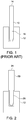
- FIG. 1 is a schematic illustration of the joining of a Golden Finger card 10 having a nominal thickness of 1.57 mm with a standard PCIe connector 12.
- the body 14 of the Golden Finger card 10 has the same 1.57 mm thickness as the finger portion 16 of the card.
- such a conventional configuration is limiting, as the only way to increase application complexity would be to implement thinner dielectric layers. However, as discussed above, such a configuration is undesirable.
- FIG. 2 is also a schematic illustration of the joining of a Golden Finger card 20 according to the present disclosure, but with two different thickness regions.
- the Golden Finger card 20 can mate with the same standard PCIe connector 12 (in FIG. 1 ). That is, the Golden Finger portion 26 has the same thickness as a conventional golden finger card, such as the Golden Finger card 10 (in FIG. 1 ). However, in addition to the Golden Finger portion 26, the Golden Finger card 20 has body portion 24 with a thickness that is different from the Golden Finger portion 26. As a result, application complexity can be increased without relying on thinner dielectric layers.
- the Golden Finger portion 26 can have the same 1.57 mm nominal thickness as to fit into a standard connector, such as the PCIe connector 12, while the body portion 24 of the Golden Finger card 20 can be thicker than the Golden finger portion 26 of the card. There is generally no limit to the thickness of the body portion 24 of the Golden Finger card 20. Further, such cards can be configured as single ladder or a double ladder cards. In certain configurations, thicknesses of 2.4 mm have been found suitable for the body portion 24 to accommodate increased application complexity, while still retaining the 1.57 mm thickness limitation of the Golden finger portion 26 in order to fit into the standard connector 12.
- FIG. 3 is a side view and construction of ladder type golden finger card. It is a 22 layer, double side ladder card, with layers 1 to 4 and 19 to 22 removed at golden finger side. Therefore, FIG. 3 is a schematic representation of a double ladder golden finger board where the body portion has a thickness greater than the golden finger portion. With a 2.4 mm board thickness, it is possible to construct 16-layer Golden Finger card with general composition (4 mil core, 16 mil prepreg). By comparison, a traditional Golden Finger card will have the specific composition (3 mil core, 3 mil prepreg) which will result in larger PCB trace loss and reduced design margins.
- Distance 35 has a mask-to-mask length of about 95.4 mils, and distance 36 has a gold finger-to-gold finger length of about 62.4 mils.
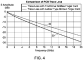
- FIG. 4 is a graphic representation of the trace loss of a traditional Golden Finger card 30, as compared to a trace loss of a ladder type Golden Finger card 32, according to the present disclosure over a range of frequencies from 0 to 20 GHz.
- the trace loss is improved for a ladder type Golden Finger, as compared to a traditional golden finger.
- the improvement is increased as frequency is increased.
- implementing a ladder type design would lead to greater design margin and higher reliability.
- the taper structure of the golden finger card is due to the mechanical characteristic features of a PCIe connector into which the golden finger card is insertable. All golden finger card should have taper in order to fit into the dimensions of a standard PCIe connector.
- the golden finger is directly connected to traces in the body portion of the board. The fingers go straight through the card to connect to traces by way of visa. They will transit to any layer by via in body of the board. However, by making the body of the board thicker beyond the finger portion of the board, there will be more dielectric material between traces. This additional dielectric material between traces is a structural feature of the boards of this disclosure which will allow for lower loss.
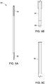
- FIG. 5A is a schematic representation of a ladder type PCB 50 containing two or more different types of board thicknesses.
- the ladder type PCB has a thickness of 1.57 mm at the Golden Fingers edge 52 and a thicker body portion thickness 54.
- FIG 5B is an enlarged view of a portion of FIG. 5A containing the Golden Fingers edge 52. It can be seen that the end of the edge 56, comprising the Golden Finger portion 26, is tapered at an angle of about 20° ⁇ 5° for the first thickness 1.4 mm ( ⁇ 0.25 mm) from the edge of the Golden Finger card 20 (in FIG. 2 ). If desired, the above taper could be placed on each side of the Golden Fingers edge portion 26, as shown in FIG. 5B .
- FIG. 5C is an enlarged view of a portion of FIG. 5A illustrating the thickness of the body portion thickness 54 of the board.
- a single ladder PCB increases the thickness of the PCB 50 by about 0.415 mm.
- a double ladder PCB would increase about 0.830 mm in thickness making the PCB 50 body thickness about 2.4 mm ( ⁇ 0.24) in total thickness.
Landscapes
- Engineering & Computer Science (AREA)
- Microelectronics & Electronic Packaging (AREA)
- Coupling Device And Connection With Printed Circuit (AREA)
- Structure Of Printed Boards (AREA)
- Printing Elements For Providing Electric Connections Between Printed Circuits (AREA)
Abstract
Description
- This disclosure relates to a Golden Finger card design where the main body of the printed circuit board ("PCB") is increased in thickness without increasing PCB finger thickness. By maintaining the width of the edge of the PCB fingers, use of existing connectors is maintained. Meanwhile, the main body of the PCB is not limited in thickness, so as to accommodate additional PCB layers and thus, increased application complexity. Golden Finger cards of this disclosure can be used as a video and graphics card, network adapter card, audio adapter card, and television or other specialty adapter card.
- A Golden Finger card is frequently used in server/storage product designs. However, due to connector limitations, the board thickness is typically standardized and fixed (normally 1.57 mm). However, as application complexity increases, the number of signal traces required also increases for Golden Finger cards. Hence, a higher layer count PCB is necessary. However, a limitation on the fixed board thickness would result in the dielectric thickness of the PCB layers becoming thinner, thereby causing higher trace loss and reduced signal margins. Thus, there is a need for Golden Finger cards that allow for an increased number of layers while maintaining connector compatibility, reduced trace loss, and high signal margins.
- A ladder type PCB contains two or more different board thicknesses. The Golden Finger edge has a first board thickness (e.g., 1.57 mm [± 0.15 mm]) so as to mate with existing connectors. However, outside of edge thickness limitations, there are no limitations on the thickness of the remainder of the board. Hence, in one embodiment of this disclosure, the main body of the board may have a larger thickness (e.g., greater than 1.57 mm). An example of such a board would have a body thickness of about twice as thick as the first thickness, or about 2.4 mm (± 0.24 mm), while the edge thickness is maintained at 1.57 mm (± 0.15 mm).
- There are no limitations for a ladder type PCB design. Hence, in another embodiment of this disclosure, the PCB could contain a one side ladder.
- In yet another embodiment of this disclosure, the PCB could have two side ladders.
- In a still further embodiment, in a PCB having a 2.4 mm board thickness (± 0.24 mm), it is possible to construct 16-layer Golden Finger card with a general composition of 4 mil core, 16 mil prepreg. By comparison, a traditional Golden Finger card will have a specific composition of 3 mil core, 3 mil prepreg, which will result in larger PCB trace loss and reduced design margins. Further particular and preferred aspects of the present invention are set out in the accompanying independent and dependent claims. Features of the dependent claims may be combined with features of the independent claims as appropriate, and in combinations other than those explicitly set out in the claims.
- The disclosure, and its advantages and drawings, will be better understood from the following description of exemplary embodiments together with reference to the accompanying drawings. These drawings depict only exemplary embodiments, and are therefore not to be considered as limitations on the scope of the various embodiments or claims.
-
FIG. 1 (Prior Art) is a schematic illustration of the joining of a golden finger card having a thickness of 1.57 mm with a standard connector. -
FIG. 2 shows the same standard connector as inFIG. 1 joined to a golden finger card of the present disclosure, where the main body of the board has a thickness of 2.4 mm while maintaining the board edge thickness at 1.57 mm. -
FIG. 3 is a schematic representation of a side view of a 2.4 mm double ladder PCB in which it is possible to construct 16-layer golden finger card with general configuration (4 mil core, 16 mil prepreg). -
FIG. 4 is a graphic representation of PCB trace loss for a traditional golden finger card, as compared to the trace loss for a ladder type golden finger card. -
FIG. 5A is a schematic depiction of a two-sided ladder golden finger card. -
FIG. 5B is an enlarged view of a portion ofFIG. 5A to show detail of the golden fingers. -
FIG. 5C is an enlarged view of a portion ofFIG. 5A to show details of the main body of the PCB. - The present invention is described with reference to the attached figures, where like reference numerals are used throughout the figures to designate similar or equivalent elements. The figures are not drawn to scale and are provided merely to illustrate the instant invention. Several aspects of the invention are described below with reference to example applications for illustration. It should be understood that numerous specific details, relationships, and methods are set forth to provide a full understanding of the invention. One having ordinary skill in the relevant art, however, will readily recognize that the invention can be practiced without one or more of the specific details, or with other methods. In other instances, well-known structures or operations are not shown in detail to avoid obscuring the invention. The present invention is not limited by the illustrated ordering of acts or events, as some acts may occur in different orders and/or concurrently with other acts or events. Furthermore, not all illustrated acts or events are required to implement a methodology in accordance with the present invention.
-
FIG. 1 (Prior Art) is a schematic illustration of the joining of a GoldenFinger card 10 having a nominal thickness of 1.57 mm with astandard PCIe connector 12. Thebody 14 of the Golden Fingercard 10 has the same 1.57 mm thickness as thefinger portion 16 of the card. As discussed above, such a conventional configuration is limiting, as the only way to increase application complexity would be to implement thinner dielectric layers. However, as discussed above, such a configuration is undesirable. - In view of the limitations of the configuration of
FIG. 1 , the configuration ofFIG. 2 is presented.FIG. 2 is also a schematic illustration of the joining of a Golden Fingercard 20 according to the present disclosure, but with two different thickness regions. As shown inFIG. 2 , the GoldenFinger card 20 can mate with the same standard PCIe connector 12 (inFIG. 1 ). That is, the Golden Fingerportion 26 has the same thickness as a conventional golden finger card, such as the Golden Finger card 10 (inFIG. 1 ). However, in addition to the Golden Fingerportion 26, the Golden Fingercard 20 hasbody portion 24 with a thickness that is different from the Golden Fingerportion 26. As a result, application complexity can be increased without relying on thinner dielectric layers. - In a particular example, the Golden
Finger portion 26 can have the same 1.57 mm nominal thickness as to fit into a standard connector, such as thePCIe connector 12, while thebody portion 24 of the Golden Fingercard 20 can be thicker than theGolden finger portion 26 of the card. There is generally no limit to the thickness of thebody portion 24 of the Golden Fingercard 20. Further, such cards can be configured as single ladder or a double ladder cards. In certain configurations, thicknesses of 2.4 mm have been found suitable for thebody portion 24 to accommodate increased application complexity, while still retaining the 1.57 mm thickness limitation of the Goldenfinger portion 26 in order to fit into thestandard connector 12. -
FIG. 3 is a side view and construction of ladder type golden finger card. It is a 22 layer, double side ladder card, withlayers 1 to 4 and 19 to 22 removed at golden finger side. Therefore,FIG. 3 is a schematic representation of a double ladder golden finger board where the body portion has a thickness greater than the golden finger portion. With a 2.4 mm board thickness, it is possible to construct 16-layer Golden Finger card with general composition (4 mil core, 16 mil prepreg). By comparison, a traditional Golden Finger card will have the specific composition (3 mil core, 3 mil prepreg) which will result in larger PCB trace loss and reduced design margins.Distance 35 has a mask-to-mask length of about 95.4 mils, anddistance 36 has a gold finger-to-gold finger length of about 62.4 mils. -
FIG. 4 is a graphic representation of the trace loss of a traditionalGolden Finger card 30, as compared to a trace loss of a ladder typeGolden Finger card 32, according to the present disclosure over a range of frequencies from 0 to 20 GHz. As shown inFIG. 4 , the trace loss is improved for a ladder type Golden Finger, as compared to a traditional golden finger. Further, as also shown inFIG. 4 , the improvement is increased as frequency is increased. Thus, implementing a ladder type design would lead to greater design margin and higher reliability. - The taper structure of the golden finger card is due to the mechanical characteristic features of a PCIe connector into which the golden finger card is insertable. All golden finger card should have taper in order to fit into the dimensions of a standard PCIe connector. The golden finger is directly connected to traces in the body portion of the board. The fingers go straight through the card to connect to traces by way of visa. They will transit to any layer by via in body of the board. However, by making the body of the board thicker beyond the finger portion of the board, there will be more dielectric material between traces. This additional dielectric material between traces is a structural feature of the boards of this disclosure which will allow for lower loss. Because the board thickness is not limited in the body side of the board, we can increase the amount of dielectric between traces, thereby limiting loss, while not affecting the dimensions of the finger portion of the board which will still fit into a standard PCIe connector.
FIG. 5A is a schematic representation of aladder type PCB 50 containing two or more different types of board thicknesses. The ladder type PCB has a thickness of 1.57 mm at theGolden Fingers edge 52 and a thickerbody portion thickness 54. -
FIG 5B is an enlarged view of a portion ofFIG. 5A containing theGolden Fingers edge 52. It can be seen that the end of theedge 56, comprising theGolden Finger portion 26, is tapered at an angle of about 20°± 5° for the first thickness 1.4 mm (± 0.25 mm) from the edge of the Golden Finger card 20 (inFIG. 2 ). If desired, the above taper could be placed on each side of the GoldenFingers edge portion 26, as shown inFIG. 5B . -
FIG. 5C is an enlarged view of a portion ofFIG. 5A illustrating the thickness of thebody portion thickness 54 of the board. A single ladder PCB increases the thickness of thePCB 50 by about 0.415 mm. A double ladder PCB would increase about 0.830 mm in thickness making thePCB 50 body thickness about 2.4 mm (± 0.24) in total thickness. - The terminology used herein is for the purpose of describing particular embodiments only and is not intended to be limiting of the invention. As used herein, the singular forms "a," "an," and "the" are intended to include the plural forms as well, unless the context clearly indicates otherwise. Furthermore, to the extent that the terms "including," "includes," "having," "has," "with," or variants thereof are used in either the detailed description and/or the claims, such terms are intended to be inclusive in a manner similar to the term "comprising."
Although particular embodiments have been described herein, it will be appreciated that the invention is not limited thereto and that many modifications and additions thereto may be made within the scope of the invention. For example, various combinations of the features of the following dependent claims can be made with the features of the independent claims without departing from the scope of the present invention.
Claims (15)
- A Golden Finger card comprising:a Golden Finger card edge (52) having a first thickness; anda Golden Finger card body portion (24), wherein the Golden Finger card body portion (24) has a thickness greater than the first thickness.
- The Golden Finger card of claim 1, wherein the Golden Finger card body portion (24) is a single sided ladder PCB.
- The Golden Finger card of claim 2, wherein the single sided ladder PCB (24) adds a thickness to only one side of a body of the single sided ladder PCB.
- The Golden Finger card of claim 1, wherein the Golden Finger card body portion (24) is a double sided ladder PCB.
- The Golden Finger card of claim 4, wherein the double sided ladder PCB (24) adds a thickness on each side of a body of double sided ladder PCB.
- The Golden Finger card of any of claims 1-5, wherein the first thickness is of a size that fits a standard connector (12).
- The Golden Finger card of any of claims 1-6, wherein the Golden Finger card edge (52) exhibits a taper (56).
- The Golden Finger card of any of claims 1-7, wherein each edge (52) of the Golden Finger card exhibits a taper (56).
- The Golden Finger card of any of claims 1-8, wherein an increased thickness of dielectric material between traces in the Golden Finger card body portion (24) exhibits a trace loss of less than 25 dB at a frequency of 20 GHz.
- A Golden Finger card comprising:a Golden Finger card edge (52) having a first thickness; anda Golden Finger card body portion (24), wherein the Golden Finger card body portion (24) has a thickness of about 1.5 times the first thickness.
- The Golden Finger card of claim 10, wherein the Golden Finger card edge (52) exhibits a taper (56).
- The Golden Finger card of claim 10 or claim 11, wherein each edge (52) of the Golden Finger card exhibits a taper (56).
- The Golden Finger card of any of claims 10-12, wherein an increased thickness of dielectric material between traces in the Golden Finger card body portion (24) exhibits a trace loss of less than 25 dB at a frequency of 20GHz.
- The Golden Finger card of any of claims 10-13, wherein the first thickness is about 1.57 mm.
- The Golden Finger card of any of claims 10-14, wherein the thickness of the Golden Finger card body portion (24) is about 2.4 mm.
Applications Claiming Priority (1)
| Application Number | Priority Date | Filing Date | Title |
|---|---|---|---|
| US16/042,208 US20200029434A1 (en) | 2018-07-23 | 2018-07-23 | Ladder type pcb for high layer count golden finger card design |
Publications (1)
| Publication Number | Publication Date |
|---|---|
| EP3599799A1 true EP3599799A1 (en) | 2020-01-29 |
Family
ID=65278188
Family Applications (1)
| Application Number | Title | Priority Date | Filing Date |
|---|---|---|---|
| EP19154723.1A Withdrawn EP3599799A1 (en) | 2018-07-23 | 2019-01-31 | Ladder type pcb for high layer count golden finger card design |
Country Status (5)
| Country | Link |
|---|---|
| US (1) | US20200029434A1 (en) |
| EP (1) | EP3599799A1 (en) |
| JP (1) | JP2020017715A (en) |
| CN (1) | CN110753444A (en) |
| TW (1) | TW202008860A (en) |
Families Citing this family (4)
| Publication number | Priority date | Publication date | Assignee | Title |
|---|---|---|---|---|
| JP6871465B1 (en) | 2020-02-05 | 2021-05-12 | ハウスウェルネスフーズ株式会社 | Ice cream-like aerated emulsified composition |
| CN111642084B (en) * | 2020-06-29 | 2021-08-31 | 苏州浪潮智能科技有限公司 | Method, device, device and storage medium for determining golden finger chamfer |
| CN113708112B (en) * | 2021-07-30 | 2023-07-14 | 苏州浪潮智能科技有限公司 | Board ladder connection structure and signal connector |
| CN115568101B (en) * | 2022-11-01 | 2024-02-27 | 清远市富盈电子有限公司 | PCB processing method and milling machine workbench used by same |
Citations (5)
| Publication number | Priority date | Publication date | Assignee | Title |
|---|---|---|---|---|
| DE102004005699A1 (en) * | 2004-02-05 | 2005-08-25 | Power Digital Card Co., Ltd., Banchiau | Memory card structure has smaller sized case formed above circuit board, and space is formed between case and circuit board, for storing electronic components |
| US20110003487A1 (en) * | 2008-02-29 | 2011-01-06 | Zte Corporation | Method for reducing the fitting thrust of golden finger and pcb |
| EP2511987A2 (en) * | 2011-04-15 | 2012-10-17 | Robert Bosch GmbH | Improved multiple direct contacting of electrical components |
| CN106937480A (en) * | 2017-03-04 | 2017-07-07 | 郑州云海信息技术有限公司 | Single board and forming method based on ladder gold finger |
| CN206962151U (en) * | 2017-07-19 | 2018-02-02 | 富加宜电子(南通)有限公司 | A kind of card insert type high speed connector card end |
Family Cites Families (9)
| Publication number | Priority date | Publication date | Assignee | Title |
|---|---|---|---|---|
| US3160455A (en) * | 1961-05-16 | 1964-12-08 | Burroughs Corp | Printed circuit boards and connectors therefor |
| US7140548B2 (en) * | 2004-01-30 | 2006-11-28 | Power Digital Card Co., Ltd. | Memory card structure |
| ITUD20040034A1 (en) * | 2004-02-27 | 2004-05-27 | Eurotech Spa | MULTILAYER EXPANSION BOARD FOR ELECTRONIC AND RELATED EQUIPMENT |
| US7547213B2 (en) * | 2004-08-26 | 2009-06-16 | Micron Technology, Inc. | Memory modules and methods for manufacturing memory modules |
| US7326857B2 (en) * | 2004-11-18 | 2008-02-05 | International Business Machines Corporation | Method and structure for creating printed circuit boards with stepped thickness |
| TWI345144B (en) * | 2007-12-21 | 2011-07-11 | Asustek Comp Inc | Expansion card |
| CN102458044A (en) * | 2010-10-19 | 2012-05-16 | 上海嘉捷通电路科技有限公司 | Novel golden finger structure |
| JP2013115110A (en) * | 2011-11-25 | 2013-06-10 | Tanaka Kikinzoku Kogyo Kk | Printed wiring board of step structure |
| CN103153000B (en) * | 2013-02-01 | 2015-07-22 | 东莞生益电子有限公司 | Manufacturing method of golden finger circuit board and circuit board manufactured by method |
-
2018
- 2018-07-23 US US16/042,208 patent/US20200029434A1/en not_active Abandoned
- 2018-12-03 TW TW107143276A patent/TW202008860A/en unknown
- 2018-12-24 CN CN201811580508.8A patent/CN110753444A/en active Pending
-
2019
- 2019-01-22 JP JP2019008778A patent/JP2020017715A/en active Pending
- 2019-01-31 EP EP19154723.1A patent/EP3599799A1/en not_active Withdrawn
Patent Citations (5)
| Publication number | Priority date | Publication date | Assignee | Title |
|---|---|---|---|---|
| DE102004005699A1 (en) * | 2004-02-05 | 2005-08-25 | Power Digital Card Co., Ltd., Banchiau | Memory card structure has smaller sized case formed above circuit board, and space is formed between case and circuit board, for storing electronic components |
| US20110003487A1 (en) * | 2008-02-29 | 2011-01-06 | Zte Corporation | Method for reducing the fitting thrust of golden finger and pcb |
| EP2511987A2 (en) * | 2011-04-15 | 2012-10-17 | Robert Bosch GmbH | Improved multiple direct contacting of electrical components |
| CN106937480A (en) * | 2017-03-04 | 2017-07-07 | 郑州云海信息技术有限公司 | Single board and forming method based on ladder gold finger |
| CN206962151U (en) * | 2017-07-19 | 2018-02-02 | 富加宜电子(南通)有限公司 | A kind of card insert type high speed connector card end |
Also Published As
| Publication number | Publication date |
|---|---|
| US20200029434A1 (en) | 2020-01-23 |
| CN110753444A (en) | 2020-02-04 |
| JP2020017715A (en) | 2020-01-30 |
| TW202008860A (en) | 2020-02-16 |
Similar Documents
| Publication | Publication Date | Title |
|---|---|---|
| US20200029434A1 (en) | Ladder type pcb for high layer count golden finger card design | |
| US10026556B2 (en) | Electronic component | |
| US20220068565A1 (en) | Electronic component | |
| JP4518103B2 (en) | Common mode choke coil | |
| US10636561B2 (en) | Common mode noise filter | |
| CN106575808B (en) | Transmission lines and electronic equipment | |
| US10147534B2 (en) | Common mode noise filter | |
| JPWO2012172939A1 (en) | Electronic component and manufacturing method thereof | |
| US20180041185A1 (en) | Common mode noise filter | |
| US8958213B2 (en) | Mounting structure of chip component | |
| US10937584B2 (en) | Common mode noise filter | |
| US10979015B2 (en) | Common-mode choke coil | |
| JP2009065198A (en) | Multilayer capacitor | |
| EP3250012A1 (en) | Power tube connecting structure of power amplifier and power amplifier | |
| US8461944B2 (en) | First and second U-shape waveguides joined to a dielectric carrier by a U-shape sealing frame | |
| US6348844B1 (en) | Transition between symmetric stripline and asymmetric stripline | |
| US11139101B2 (en) | Coil component | |
| US20250125083A1 (en) | Inductor component | |
| CN105682342B (en) | Circuit board and terminal | |
| DE102013113861A1 (en) | Galvanic separation device for process measuring devices | |
| JP2007324251A (en) | Laminated capacitor | |
| JP2006156079A (en) | Flexible flat cable | |
| CN223829513U (en) | Circuit boards and electronic products | |
| US11792919B2 (en) | Case with isolation barriers | |
| US20250299857A1 (en) | Coil component |
Legal Events
| Date | Code | Title | Description |
|---|---|---|---|
| PUAI | Public reference made under article 153(3) epc to a published international application that has entered the european phase |
Free format text: ORIGINAL CODE: 0009012 |
|
| STAA | Information on the status of an ep patent application or granted ep patent |
Free format text: STATUS: THE APPLICATION HAS BEEN PUBLISHED |
|
| AK | Designated contracting states |
Kind code of ref document: A1 Designated state(s): AL AT BE BG CH CY CZ DE DK EE ES FI FR GB GR HR HU IE IS IT LI LT LU LV MC MK MT NL NO PL PT RO RS SE SI SK SM TR |
|
| AX | Request for extension of the european patent |
Extension state: BA ME |
|
| STAA | Information on the status of an ep patent application or granted ep patent |
Free format text: STATUS: REQUEST FOR EXAMINATION WAS MADE |
|
| 17P | Request for examination filed |
Effective date: 20200621 |
|
| RBV | Designated contracting states (corrected) |
Designated state(s): AL AT BE BG CH CY CZ DE DK EE ES FI FR GB GR HR HU IE IS IT LI LT LU LV MC MK MT NL NO PL PT RO RS SE SI SK SM TR |
|
| STAA | Information on the status of an ep patent application or granted ep patent |
Free format text: STATUS: EXAMINATION IS IN PROGRESS |
|
| STAA | Information on the status of an ep patent application or granted ep patent |
Free format text: STATUS: THE APPLICATION HAS BEEN WITHDRAWN |
|
| 17Q | First examination report despatched |
Effective date: 20211214 |
|
| 18W | Application withdrawn |
Effective date: 20211229 |