EP3598667A1 - Optical signal power control method and device, and optical line terminal - Google Patents
Optical signal power control method and device, and optical line terminal Download PDFInfo
- Publication number
- EP3598667A1 EP3598667A1 EP18766962.7A EP18766962A EP3598667A1 EP 3598667 A1 EP3598667 A1 EP 3598667A1 EP 18766962 A EP18766962 A EP 18766962A EP 3598667 A1 EP3598667 A1 EP 3598667A1
- Authority
- EP
- European Patent Office
- Prior art keywords
- onu
- registration
- gain
- attenuation
- optical
- Prior art date
- Legal status (The legal status is an assumption and is not a legal conclusion. Google has not performed a legal analysis and makes no representation as to the accuracy of the status listed.)
- Granted
Links
Images






Classifications
-
- H—ELECTRICITY
- H04—ELECTRIC COMMUNICATION TECHNIQUE
- H04B—TRANSMISSION
- H04B10/00—Transmission systems employing electromagnetic waves other than radio-waves, e.g. infrared, visible or ultraviolet light, or employing corpuscular radiation, e.g. quantum communication
- H04B10/07—Arrangements for monitoring or testing transmission systems; Arrangements for fault measurement of transmission systems
- H04B10/075—Arrangements for monitoring or testing transmission systems; Arrangements for fault measurement of transmission systems using an in-service signal
- H04B10/077—Arrangements for monitoring or testing transmission systems; Arrangements for fault measurement of transmission systems using an in-service signal using a supervisory or additional signal
- H04B10/0773—Network aspects, e.g. central monitoring of transmission parameters
-
- H—ELECTRICITY
- H04—ELECTRIC COMMUNICATION TECHNIQUE
- H04B—TRANSMISSION
- H04B10/00—Transmission systems employing electromagnetic waves other than radio-waves, e.g. infrared, visible or ultraviolet light, or employing corpuscular radiation, e.g. quantum communication
- H04B10/29—Repeaters
- H04B10/291—Repeaters in which processing or amplification is carried out without conversion of the main signal from optical form
- H04B10/293—Signal power control
- H04B10/294—Signal power control in a multiwavelength system, e.g. gain equalisation
-
- H—ELECTRICITY
- H04—ELECTRIC COMMUNICATION TECHNIQUE
- H04B—TRANSMISSION
- H04B10/00—Transmission systems employing electromagnetic waves other than radio-waves, e.g. infrared, visible or ultraviolet light, or employing corpuscular radiation, e.g. quantum communication
- H04B10/27—Arrangements for networking
- H04B10/272—Star-type networks or tree-type networks
-
- H—ELECTRICITY
- H04—ELECTRIC COMMUNICATION TECHNIQUE
- H04B—TRANSMISSION
- H04B10/00—Transmission systems employing electromagnetic waves other than radio-waves, e.g. infrared, visible or ultraviolet light, or employing corpuscular radiation, e.g. quantum communication
- H04B10/29—Repeaters
- H04B10/291—Repeaters in which processing or amplification is carried out without conversion of the main signal from optical form
- H04B10/293—Signal power control
-
- H—ELECTRICITY
- H04—ELECTRIC COMMUNICATION TECHNIQUE
- H04B—TRANSMISSION
- H04B10/00—Transmission systems employing electromagnetic waves other than radio-waves, e.g. infrared, visible or ultraviolet light, or employing corpuscular radiation, e.g. quantum communication
- H04B10/50—Transmitters
- H04B10/564—Power control
Definitions
- the present disclosure relates to the field of communication, and particularly, to an optical signal power control method and device, and an optical line terminal.
- PON passive optical network
- EPON Ethernet Passive Optical Network
- GPON Gight-Capable Passive Optical Network
- 10GEPON 10GEPON
- XGPON XGPON
- NGPON2 10GEPON
- bandwidth in the access technology is constantly increased.
- the increase in bandwidth brings about a problem of insufficient power budget, because too many users on the access network requires a high power budget to make receiving of light powers at both a central office and a terminal meet sensitivity requirements and achieve good transmission performance.
- an optical amplifier is required.
- Optical amplifiers commonly used in current communication systems are Erbium-doped Optical Fiber Amplifiers (EDFAs) and Semiconductor Optical Amplifiers (SOAs). Due to advantages including a relatively flat and wide gain spectrum, fast dynamic response, and integratability, SOA has attracted more and more attention and become a good choice for optical amplifier components in the optical access field.
- EDFAs Erbium-doped Optical Fiber Amplifiers
- SOAs Semiconductor Optical Amplifiers Due to advantages including a relatively flat and wide gain spectrum, fast dynamic response, and integratability, SOA has attracted more and more attention and become a good choice for optical amplifier components in the optical access field.
- a dynamic range problem is present in the PON system. Due to different light transmitting powers of different optical network units (ONUs), and different distances from different ONUs to an optical line terminal (OLT), the OLT receives different light powers of different ONUs. If the SOA maintains the same gain, it may cause insufficiently amplified receiving light of some ONUs that fails to meet the OLT sensitivity requirements, while causing excessively amplified receiving light of some other ONUs that leads to overload of the OLT and even damages to an OLT receiver. Therefore, a mechanism to control an output light power of the SOA is required so that the SOA can reasonably adjust the gain according to different incident light powers, or to add a variable attenuation after the SOA to make the emitting light have a relatively uniform power.
- an optical signal power control method and device In order to solve at least the problem of equalizing uplink burst signal amplification in an ONU, an optical signal power control method and device, and an optical line terminal are provided in the embodiments of the present disclosure.
- an optical signal power control method including: acquiring different time points when uplink optical signals of optical network units (ONUs) arrive at an optical signal amplifier or a variable optical attenuator; establishing a correspondence relationship between an ONU ID and a power control factor of the uplink optical signals; and performing power control on the uplink optical signals according to the different time points and the correspondence relationship.
- ONUs optical network units
- the power control factor includes at least one of: a gain of the optical signal amplifier, and an attenuation of the variable optical attenuator.
- the step of establishing the correspondence relationship between the ONU ID and the power control factor of the uplink optical signals includes: allocating a registration time slot and transmitting a downlink registration signal; and starting, when the ONU receives the downlink registration signal and determines that a power requirement of the registration time slot is met, registration and establishment of a correspondence relationship between the ONU ID and the gain of the optical signal amplifier.
- the step of establishing the correspondence relationship between the ONU ID and the power control factor of the uplink optical signals includes: allocating a registration time slot and transmitting a downlink registration signal, wherein the downlink registration signal includes gain information of the optical signal amplifier; increasing, when the ONU receives the downlink registration signal and determines that the downlink registration signal is in a registration time slot with a minimum gain of the optical signal amplifier, the gain of the optical signal amplifier until a serial number transmitted by the ONU is correctly received; and establishing a correspondence relationship between the ONU ID and the gain of the optical signal amplifier.
- the step of establishing the correspondence relationship between the ONU ID and the power control factor of the uplink optical signals includes: allocating a registration time slot and transmitting a downlink registration signal, wherein the registration time slot is pre-assigned an attenuation value; and starting, when the ONU receives the downlink registration signal and determines that a power requirement of the registration time slot is met, registration and establishment of an attenuation correspondence relationship between the ONU ID and the variable optical attenuator.
- the step of establishing the correspondence relationship between the ONU ID and the power control factor of the uplink optical signals includes: setting the attenuation of the variable optical attenuator to maximum; allocating a registration time slot and transmitting a downlink registration signal, wherein the downlink registration signal includes attenuation information of the variable optical attenuator; decreasing, when the ONU receives the downlink registration signal and determines that the downlink registration signal is in a registration time slot with a minimum actual gain of the optical signal amplifier, the attenuation of the variable optical attenuator until a serial number transmitted by the ONU is correctly received; and establishing an attenuation relationship between the ONU ID and the variable optical attenuator.
- the step of establishing the correspondence relationship between the ONU ID and the power control factor of the uplink optical signals includes: allocating a registration time slot and transmitting a downlink registration signal, wherein in the registration time slot, the optical signal amplifier is provided with a pre-assigned gain, and the variable optical attenuator is provided with a pre-assigned attenuation; and starting, when the ONU receives the downlink registration signal and determines that a power requirement of the registration time slot is met, registration and establishment of a correspondence relationship between the ONU ID, the gain of the optical signal amplifier, and the attenuation of the variable optical attenuator.
- the step of establishing the correspondence relationship between the ONU ID and the power control factor of the uplink optical signals includes: setting an actual gain of the optical signal amplifier to minimum; allocating a registration time slot and transmitting a downlink registration signal, wherein the downlink registration signal includes actual gain information of the optical signal amplifier; increasing, when the ONU receives the downlink registration signal and determines that the downlink registration signal is in a registration time slot with a minimum actual gain of the optical signal amplifier, the gain of the optical signal amplifier until a serial number transmitted by the ONU is correctly received; and establishing a correspondence relationship between the ONU ID, the gain of the optical signal amplifier, and the attenuation of the variable optical attenuator.
- a plurality of optical signal amplifiers or variable optical attenuators are provided.
- the uplink optical signals are subjected to corresponding power control via a shared optical signal amplifier.
- each of the plurality of correspondence relationships is a relationship between each channel of ONU IDs and a power control factor of the corresponding uplink optical signals.
- an optical signal power control device including: an acquisition module configured to acquire different time points when uplink optical signals of optical network units (ONUs) arrive at an optical signal amplifier; an establishment module configured to establish a correspondence relationship between an ONU ID and a power control factor of the uplink optical signals; and a control module configured to perform power control on the uplink optical signals according to the different time points and the correspondence relationship.
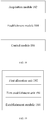
- an acquisition module configured to acquire different time points when uplink optical signals of optical network units (ONUs) arrive at an optical signal amplifier
- an establishment module configured to establish a correspondence relationship between an ONU ID and a power control factor of the uplink optical signals
- a control module configured to perform power control on the uplink optical signals according to the different time points and the correspondence relationship.
- the power control factor includes at least one of: a gain of the optical signal amplifier, and an attenuation of the variable optical attenuator.
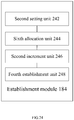
- the establishment module includes: a first allocation unit configured to allocate a registration time slot and transmit a downlink registration signal when the power control factor is a gain of the optical signal amplifier; and a first establishment unit configured to start, when the ONU receives the downlink registration signal and determines that a power requirement of the registration time slot is met, registration and establishment of a correspondence relationship between the ONU ID and the gain of the optical signal amplifier.
- the establishment module includes: a second allocation unit configured to allocate a registration time slot and transmit a downlink registration signal when the power control factor is a gain of the optical signal amplifier, wherein the downlink registration signal includes gain information of the optical signal amplifier; a first increment unit configured to increase, when the ONU receives the downlink registration signal and determines that the downlink registration signal is in a registration time slot with a minimum gain of the optical signal amplifier, the gain of the optical signal amplifier until a serial number transmitted by the ONU is correctly received; and a second establishment unit configured to establish a correspondence relationship between the ONU ID and the gain of the optical signal amplifier.
- the establishment module includes: a third allocation unit configured to allocate a registration time slot and transmit a downlink registration signal when the power control factor is an attenuation of the variable optical attenuator, wherein the registration time slot is pre-assigned an attenuation value; and a third establishment unit configured to start, when the ONU receives the downlink registration signal and determines that a power requirement of the registration time slot is met, registration and establishment of an attenuation correspondence relationship between the ONU ID and the variable optical attenuator.
- the establishment module includes: a first setting unit configured to set, when the power control factor is an attenuation of the variable optical attenuator, the attenuation of the variable optical attenuator to maximum; a fourth allocation unit configured to allocate a registration time slot and transmit a downlink registration signal, wherein the downlink registration signal includes attenuation information of the variable optical attenuator; a decrement unit configured to decrease, when the ONU receives the downlink registration signal and determines that the downlink registration signal is in a registration time slot with a minimum actual gain of the optical signal amplifier, the attenuation of the variable optical attenuator until a serial number transmitted by the ONU is correctly received; and a fourth establishment unit configured to establish an attenuation relationship between the ONU ID and the variable optical attenuator.
- the establishment module includes: a fifth allocation unit configured to allocate a registration time slot and transmit a downlink registration signal when the power control factor is a gain of the optical signal amplifier and an attenuation of the variable optical attenuator, wherein in the registration time slot, the optical signal amplifier is provided with a pre-assigned gain, and the variable optical attenuator is provided with a pre-assigned attenuation; and a fifth establishment unit configured to start, when the ONU receives the downlink registration signal and determines that a power requirement of the registration time slot is met, registration and establishment of a correspondence relationship between the ONU ID, the gain of the optical signal amplifier, and the attenuation of the variable optical attenuator.
- a fifth allocation unit configured to allocate a registration time slot and transmit a downlink registration signal when the power control factor is a gain of the optical signal amplifier and an attenuation of the variable optical attenuator, wherein in the registration time slot, the optical signal amplifier is provided with a pre-assigned gain, and the
- the establishment module includes: a second setting unit configured to set an actual gain of the optical signal amplifier to minimum when the power control factor is a gain of the optical signal amplifier and an attenuation of the variable optical attenuator; a sixth allocation unit configured to allocate a registration time slot and transmit a downlink registration signal, wherein the downlink registration signal includes actual gain information of the optical signal amplifier; a second increment unit configured to increase, when the ONU receives the downlink registration signal and determines that the downlink registration signal is in a registration time slot with a minimum actual gain of the optical signal amplifier, the gain of the optical signal amplifier until a serial number transmitted by the ONU is correctly received; and a sixth establishment unit configured to establish a correspondence relationship between the ONU ID, the gain of the optical signal amplifier, and the attenuation of the variable optical attenuator.
- a plurality of optical signal amplifiers or variable optical attenuators are provided.
- the uplink optical signals are subjected to corresponding power control via a shared optical signal amplifier.
- each of the plurality of correspondence relationships is a relationship between each channel of ONU IDs and a power control factor of the corresponding uplink optical signals.
- an optical line terminal including a device as described above.
- a storage medium configured to store a program code for performing the steps of: acquiring different time points when uplink optical signals of optical network units (ONUs) arrive at an optical signal amplifier or a variable optical attenuator; establishing a correspondence relationship between an ONU ID and a power control factor of the uplink optical signals; and performing power control on the uplink optical signals according to the different time points and the correspondence relationship.
- ONUs optical network units
- an electronic device including a memory storing a computer program thereon, and a processor configured to execute the computer program to perform steps of any of the method embodiments as described above.
- the uplink burst signals of the ONU are amplified to a range receivable by the OLT receiver, thereby solving the problem of equalizing uplink burst signal amplification in an optical network unit (ONU) in the related art, and achieving the technical effect of reducing requirements on the receiving power range of the OLT receiver.
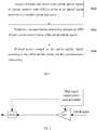
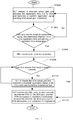
- FIG. 1 is a flowchart of an optical signal power control method according to an embodiment of the present disclosure. As shown in Fig. 1 , the flow includes the following steps S102 to S106:
- the application scenarios of the foregoing optical signal amplification method include, but are not limited to: a Passive Optical Network (PON).
- PON Passive Optical Network
- ONUs optical network units
- the uplink burst signals of the ONU are amplified to a range receivable by the OLT receiver, thereby solving the problem of equalizing uplink burst signal amplification in an optical network unit (ONU) in the related art, and achieving the technical effect of reducing requirements on the receiving power range of the OLT receiver.
- the number of optical signal amplifiers includes but is not limited to: one or more than one; and the number of variable optical attenuators includes but is not limited to: one or more than one.
- the optical signal amplifier is mainly described taking a semiconductor amplifier (SOA) as an example.
- SOA semiconductor amplifier
- a time point when each ONU uplink signal arrives at the SOA may be acquired by DBA (Dynamic Bandwidth Allocation).
- DBA Dynamic Bandwidth Allocation
- an SOA gain, or an attenuation of a variable optical attenuator (VOA) behind the SOA, or both the SOA gain and the VOA attenuation are adjusted by a DBA-based output power control module, thereby amplifying the ONU uplink burst signals to a range receivable by the OLT receiver to obtain an amplified effect and reducing requirements on the receiving power range of the OLT receiver.
- VOA variable optical attenuator
- the above power control factor includes, but is not limited to, a gain of the optical signal amplifier, and an attenuation of the variable optical attenuator.
- the step of establishing the correspondence relationship between the ONU ID and the power control factor of the uplink optical signals includes the following steps S11 to S12:
- the uplink burst signals of the ONU are further amplified to a range receivable by the OLT receiver, thereby solving the problem of equalizing uplink burst signal amplification in an optical network unit (ONU) in the related art, and achieving the technical effect of reducing requirements on the receiving power range of the OLT receiver.
- ONU optical network unit
- the step of establishing the correspondence relationship between the ONU ID and the power control factor of the uplink optical signals includes the following steps S13 to S15:
- the step of establishing the correspondence relationship between the ONU ID and the power control factor of the uplink optical signals includes the following steps S21 to S22:
- the uplink burst signals of the ONU are further amplified to a range receivable by the OLT receiver, thereby solving the problem of equalizing uplink burst signal amplification in an optical network unit (ONU) in the related art, and achieving the technical effect of reducing requirements on the receiving power range of the OLT receiver.
- ONU optical network unit
- the step of establishing the correspondence relationship between the ONU ID and the power control factor of the uplink optical signals includes the following steps S23 to S26:
- the step of establishing the correspondence relationship between the ONU ID and the power control factor of the uplink optical signals includes the following steps S31 to S32:
- the uplink burst signals of the ONU are further amplified to a range receivable by the OLT receiver, thereby solving the problem of equalizing uplink burst signal amplification in an optical network unit (ONU) in the related art, and achieving the technical effect of reducing requirements on the receiving power range of the OLT receiver.
- ONU optical network unit
- the step of establishing the correspondence relationship between the ONU ID and the power control factor of the uplink optical signals includes the following steps S33 to S36:
- a plurality of optical signal amplifiers or variable optical attenuators are provided.
- a plurality of correspondence relationships are provided, wherein each of the plurality of correspondence relationships is a relationship between each channel of ONU IDs and a power control factor of the corresponding uplink optical signals.
- the uplink optical signals are subjected to corresponding power control via a shared optical signal amplifier.
- This optional embodiment is divided into two steps.
- a relationship between the ONU ID and the SOA gain is established in a registration stage.
- a dynamic gain adjustment table is established with reference to DBA and according to the obtained relationship, wherein a DBA-based output power control module dynamically adjusts the SOA gain according to the table so that powers of the optical signals emitted by each of the ONUs are amplified, and the amplified powers tend to be the same.
- the first step a correspondence relationship between the ONU ID and the SOA gain is established.
- a dynamic range of the ODN may be up to 15 dB, and a fluctuation range of the light transmitting power of the ONU may be up to 5 dB.
- a difference in the light powers reaching the OLT receiver may be up to 20 dB. If the SOA gain is set too small, some ONUs with greater signal attenuations to the OLT cannot be registered. However, if the SOA gain is set too large, some ONUs with smaller signal attenuations to the OLT may have excessively amplified light powers, thereby damaging the OLT optical receiver.
- a suitable method is needed to enable the OLT to correctly receive uplink burst information from the ONU with an appropriate gain, record the ONU ID and the SOA gain value at that time, and establish a relationship between the two.
- Two ONU registration methods are provided below.
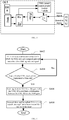
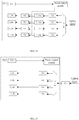
- Fig. 3 is a system block diagram during ONU registration.
- the OLT includes a medium access layer (MAC), a DBA module, a light emitting module (Tx), a light receiving module (Rx) capable of measuring a light power, a filter for filtering noises of SOA amplified spontaneous emission (ASE), an SOA, and a DBA-based output power control module.
- the DBA-based output power control module may consist of a memory, a controller and a driver.
- the memory is used for storing a dynamic gain adjustment table, according to the dynamic gain adjustment table, the controller controls the driver to drive the SOA and change the SOA gain.
- the controller may also directly receive a command from the OLT to adjust the SOA gain.
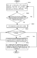
- a first ONU registration method as shown in Fig. 3 , the OLT allocates registration time slots in segments.
- the SOA has a pre-assigned gain that is set according to a power range that may be incident on the SOA and a receiving light power range of the OLT receiver. For example, provided that a system dynamic range is 20 dB, an incident light power range on SOA is [-40 dBm, -20 dBm], and a receiving power range of the OLT receiver is [-28 dBm, -8 dBm], then two registration time slots may be allocated in segments, and each of the two registration time slots correspond to the pre-assigned SOA gain values of lOdB and 15dB, respectively.
- the ONU corresponding to the incident power on SOA of [-40dBm, -30dBm] may be registered in the time slot with an SOA gain of 15dB
- the ONU corresponding to the incident power on SOA of [- 30dBm, - 20dBm] may be registered in the time slot with an SOA gain of lOdB.
- the OLT allocates a gain to the SOA through the DBA-based output power control module and transmits a downlink signal containing the light transmitting power information of the OLT, and notifies an eligible ONU to transmit an uplink signal.
- the eligible ONU refers to an ONU in which a value obtained by the ONU transmitting power subtracting uplink attenuation, that is, the incident power value on SOA, falls into a power range specified by the time slot.
- the ONU calculates the uplink attenuation according to the received downlink optical signal power.
- the uplink attenuation is obtained by the light transmitting power of the OLT subtracting a downlink optical signal power value received by the ONU.
- the ONU determines whether the uplink light power to the SOA meets the power requirement of the allocated time slot based on a value obtained by a light transmitting power of a transmitter of its own subtracting the value of the uplink attenuation, if not, waits for the next allocated time slot; if yes, transmits an uplink ONU serial number to start registration.
- the uplink signal is amplified by the SOA with the pre-assigned gain and then filtered by the filter to remove ASE noises.
- the receiver receives the filtered signal, measures the light power of the same, and converts the optical signal into an electrical signal to be transmitted to the MAC.
- the OLT records the gain value of the SOA and the ONU ID at this time, completes the registration, and establishes a relationship between the ONU ID and the SOA gain.
- the flowchart is shown in Fig. 4 .
- Table 1 ONU-ID Gain [dB] 1 G 1 2 G 2 3 G 1 4 G 2 5 G 2 ... ... n Gn
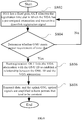
- a second registration method the OLT assigns a minimum gain, for example, 5dB, to the SOA through the DBA-based output power control module, and then allocates the registration time slot and transmits a downlink registration signal including a current SOA gain value.
- the ONU determines whether the registration signal is in the registration time slot with the minimum SOA gain, if yes, transmits uplink serial number information; if no, waits for the registration time slot with the minimum SOA gain.
- the uplink optical signal is amplified by the SOA, and filtered by the ASE filter before being received by the OLT receiver.
- the OLT receives correctly, the current ONU ID and SOA gain value are recorded to establish a relationship between the ONU ID and the SOA gain; if the OLT fails to receive correctly, the OLT increases the SOA gain by a fixed value, for example, 5dB, and the above steps are repeated. After the SOA gain is increased to a certain value, the OLT may correctly receive the ONU uplink signals. At this time, the ONU ID and the SOA gain are recorded to establish a relationship between the ONU ID and the SOA gain, and then the registration is completed.
- the flowchart is shown in Fig. 5 .
- the OLT calculates a time point when each of the ONU optical signal reaches the SOA according to the DBA and the link delay, and establishes a dynamic gain adjustment table based on the relationship between the ONU ID and the SOA gain obtained from the registration process, as shown in Fig. 2 , so as to adjust the SOA gain value dynamically by the DBA-based output power control module so that each of the ONUs tends to have the same burst optical signal power.
- Table 2 ONU-ID Time point of arriving at OLT Burst duration Gain (dB) 1 t 1 a G 1 2 t 2 b G 2 3 t 3 c G 1 4 t 4 d G 2 5 t 5 e G 2 ... ... ... ... ... n tn n Gn
- the OLT may fine-tune the SOA gain according to the received ONU light power so that the uplink light power reaches an optimal receiving power of the OLT receiver, for example, -18 dBm, after being amplified by the SOA. Then, the ONU ID and the SOA gain at this time are recorded so that each ONU has a one-to-one SOA gain. In this way, the uplink optical signals of each ONU may be amplified to a consistent optimal receiving power of the OLT receiver.
- the gain equalization amplification module in Fig. 6 can be composed of the components of Fig. 2 .
- the burst optical signals of different ONUs obtain a light power adjusted to the optimal receiving power of the OLT receiver after being amplified by the gain equalization amplification module, thereby increasing the power budget while greatly reducing requirements of the OLT receiver on the dynamic bandwidth range.
- a value of the VOA behind the SOA is dynamically adjusted according to the DBA.
- Optional Embodiment II is similar to Optional Embodiment I except that the receiving power of the OLT receiver is adjusted by adjusting attenuation.
- SOA actual gain SOA fixed gain ⁇ VOA attenuation
- the DBA-based output power control module may consist of a memory, a controller and a stepping motor for adjusting VOA attenuation.
- a relationship between the ONU ID and the VOA attenuation is established.
- a first ONU registration method as shown in Fig. 7 , the SOA is operated at a fixed gain, and the OLT allocates registration time slots in segments. In each time slot, the VOA has pre-assigned attenuation that is set according to a power range that may be incident on the SOA and a receiving light power range of the OLT receiver.
- a system dynamic range is 20 dB
- the SOA is operated at a fixed gain of 20dB
- an incident light power range on SOA is [-40 dBm, -20 dBm]
- a receiving power range of the OLT receiver is [-28 dBm, -8 dBm]
- two registration time slots may be allocated in segments, and each of the two registration time slots correspond to the pre-assigned VOA attenuation values lOdB and 5dB, respectively.
- the ONU corresponding to the incident power on SOA of [-40dBm, -30dBm] may be registered in the time slot with a VOA attenuation of 5dB
- the ONU corresponding to the incident power on SOA of [- 30dBm, - 20dBm] may be registered in the time slot with a VOA attenuation of lOdB.
- the OLT allocates attenuation to the VOA through the DBA-based output power control module and transmits a downlink signal which notifies an eligible ONU to transmit an uplink signal.
- the eligible ONU refers to an ONU in which a value obtained by the ONU transmitting power subtracting uplink attenuation, that is, the incident power value on SOA, falls into a power range specified by the time slot.
- the ONU calculates the uplink attenuation according to the received downlink optical signal power.
- the uplink attenuation is obtained by the light transmitting power of the OLT subtracting a downlink optical signal power value received by the ONU.
- the ONU determines whether the uplink light power to the SOA meets the power requirement of the allocated time slot based on a value obtained by a light transmitting power of a transmitter of its own subtracting the value of the uplink attenuation, if not, waits for the next allocated time slot; if yes, transmits an uplink ONU serial number to start registration.
- the uplink signal is amplified by the SOA with the fixed gain, attenuated by the VOA, and then filtered by the filter to remove ASE noises.
- the receiver receives the filtered signal, measures the light power of the same, and converts the optical signal into an electrical signal to be transmitted to the MAC.
- the OLT records the attenuation value of the VOA and the ONU ID at this time, completes the registration, and establishes a relationship between the ONU ID and the VOA attenuation.
- the flowchart is shown in Fig. 8 .
- a second registration method the OLT assigns a maximum attenuation, for example, lOdB, to the VOA through the DBA-based output power control module, then allocates the registration time slot and transmits a downlink registration signal including a current SOA actual gain value (Equation 1).
- the ONU determines whether it is in the registration time slot with the minimum SOA actual gain, if yes, transmits uplink serial number information; if no, waits for the registration time slot with the minimum SOA actual gain.
- the uplink optical signal is amplified by the SOA, attenuated by the VOA, and filtered by the ASE filter before being received by the OLT receiver.
- the OLT receives correctly, the current ONU ID and VOA attenuation value are recorded to establish a relationship between the ONU ID and the VOA attenuation; if the OLT fails to receive correctly, the OLT decreases the VOA attenuation by a fixed value, for example, 5dB, and the above steps are repeated. After the VOA attenuation is decreased to a certain value, the OLT may correctly receive the ONU uplink signals. At this time, the ONU ID and the VOA attenuation are recorded to establish a relationship between the ONU ID and the VOA attenuation, and then the registration is completed. The flowchart is shown in Fig. 9 .
- the OLT calculates a time point when each of the ONU optical signal reaches the VOA according to the DBA and the link delay, and establishes a dynamic gain adjustment table based on the relationship between the ONU ID and the VOA attenuation obtained from the registration process, as shown in Fig. 4 , so as to adjust the VOA attenuation value dynamically by the DBA-based output power control module so that each of the ONUs tends to have the same burst optical signal power.
- the OLT may fine-tune the VOA attenuation according to the received ONU light power so that the uplink light power reaches an optimal receiving power of the OLT receiver, for example, -18 dBm, after being amplified by the SOA and attenuated by the VOA. Then, the ONU ID and the VOA attenuation at this time are recorded so that each ONU has a one-to-one VOA attenuation. In this way, the uplink optical signals of each ONU may be amplified to the same optimal receiving power of the OLT.
- an optimal receiving power of the OLT receiver for example, -18 dBm
- Optional Embodiment III is similar to Optional Embodiments I and II except that the receiving power of the OLT receiver is adjusted by adjusting both the SOA gain and the VOA attenuation. This has the advantage of reducing requirements on the adjusting range of the SOA and the VOA.
- SOA actual gain SOA gain ⁇ VOA attenuation
- the DBA-based output power control module may consist of a memory, a controller, a driver for adjusting an SOA gain and a stepping motor for adjusting VOA attenuation.
- a relationship between the ONU ID, the SOA gain, and the VOA attenuation is established.
- a first ONU registration method the OLT allocates registration time slots in segments.
- the SOA is provided with a pre-assigned gain
- the VOA is provided with a pre-assigned attenuation
- a difference between the two is called an SOA actual gain.
- This pre-assigned actual gain is set according to a power range that may be incident on the SOA and a receiving light power range of the OLT receiver.
- a system dynamic range is 20 dB
- an incident light power range on SOA is [-40 dBm, -20 dBm]
- a receiving power range of the OLT receiver is [-28 dBm, -8 dBm]
- two registration time slots may be allocated in segments, and each of the two registration time slots correspond to the pre-assigned SOA actual gain values lOdB and 15dB, respectively.
- the SOA gain may be 15dB
- the VOA attenuation may be 5dB
- the actual gain value is 15dB
- the SOA gain may be 17dB
- the VOA attenuation may be 2dB.
- the SOA or the VOA alone when desired to be adjusted by a range of 5dB, adjusting both of them may decrease the range to 2dB and 3dB.
- the ONU corresponding to the incident power on SOA of [-40 dBm, -30 dBm] may be registered in a time slot with an SOA actual gain of 5dB, and the ONU corresponding to the incident power on SOA of [- 30dBm, - 20dBm] may be registered in the time slot with an SOA actual power of lOdB.
- the OLT assigns a gain to the SOA, and attenuation to the VOA through the DBA-based output power control module, and transmits a downlink signal that notifies an eligible ONU to transmit an uplink signal.
- the eligible ONU refers to an ONU in which a value obtained by the ONU transmitting power subtracting an uplink attenuation, that is, the incident power value on SOA, falls into a power range specified by the time slot.
- the ONU calculates the uplink attenuation according to the received downlink optical signal power.
- the uplink attenuation is obtained by the light transmitting power of the OLT subtracting a downlink optical signal power value received by the ONU.
- the ONU determines whether the uplink light power to the SOA meets the power requirement of the allocated time slot based on a value obtained by a light transmitting power of a transmitter of its own subtracting the value of the uplink attenuation, if not, waits for the next allocated time slot; if yes, transmits an uplink ONU serial number to start registration.
- the uplink signal is amplified by the SOA, attenuated by the VOA, and then filtered by the filter to remove ASE noises.
- the receiver receives the filtered signal, measures the light power of the same, and converts the optical signal into an electrical signal to be transmitted to the MAC.
- the OLT records the SOA gain value, the VOA attenuation value, and the ONU ID at this time, completes the registration, and establishes a relationship between the ONU ID, the SOA gain and the VOA attenuation.
- the flowchart is shown in Fig. 10 .
- a second registration method the OLT assigns a minimum actual gain, for example, 5dB, to the SOA through the DBA-based output power control module. This actual gain may be obtained from an SOA gain of lOdB and a VOA attenuation of 5dB.
- the OLT then allocates the registration time slot and transmits a downlink registration signal including a current SOA actual gain value (Equation 2).
- the ONU determines whether it is in the registration time slot with the minimum SOA actual gain, if yes, transmits uplink serial number information; if no, waits for the registration time slot with the minimum SOA actual gain.
- the uplink optical signal is amplified by the SOA, attenuated by the VOA, and filtered by the ASE filter before being received by the OLT receiver. If the OLT receives correctly, the current ONU ID, SOA gain value, and VOA attenuation value are recorded to establish a relationship between the ONU ID, the SOA gain, and the VOA attenuation; if the OLT fails to receive correctly, the OLT increases the SOA actual gain by a fixed value, for example, 5dB, for example, by increasing the SOA gain to 13dB and decreasing the VOA attenuation to 3dB, and then the above steps are repeated. After the SOA actual gain is increased to a certain value, the OLT may correctly receive the ONU uplink signals.
- the ONU ID, the SOA gain, and the VOA attenuation are recorded to establish a relationship between the ONU ID, the SOA gain, and the VOA attenuation, and then the registration is completed.
- the flowchart is shown in Fig. 11 .
- the OLT calculates a time point when each of the ONU optical signal reaches the SOA according to the DBA and the link delay, and establishes a dynamic gain adjustment table based on the relationship between the ONU ID, the SOA gain, and the VOA attenuation obtained from the registration process, as shown in Fig. 6 , so as to adjust the SOA gain value and the VOA attenuation value dynamically by the DBA-based output power control module so that each of the ONUs tends to have the same burst optical signal power.
- the OLT may fine-tune the SOA gain and the VOA attenuation according to the received ONU light power so that the uplink light power reaches an optimal receiving power of the OLT receiver, for example, -18 dBm, after being amplified by the SOA and attenuated by the VOA. Then, the ONU ID, the SOA gain, and the VOA attenuation at this time are recorded so that each ONU has a one-to-one SOA gain and VOA attenuation. In this way, the uplink optical signals of each ONU may be amplified to the same optimal receiving power of the OLT.
- an optimal receiving power of the OLT receiver for example, -18 dBm
- a multi-channel amplification architecture and a method for equalizing amplification output powers of each channel based on the architecture, and an OLT for the same are provided.
- This optional embodiment solves not only the problem of power equalization of each channel, but also the problem of different powers of different channels entering the SOA and an unchangeable SOA gain due to a shared SOA of different channels.
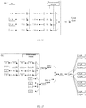
- an uplink signal line is amplified by an SOA for the first time, and then divided into four signals with different wavelengths through WDM (Wavelength Division Multiplex).
- WDM Widelength Division Multiplex
- Each of the signals is amplified by the SOA again, filtered by a filter to remove ASE noises, attenuated by a variable optical attenuator (VOA), and finally enters the receiver with a proper power.
- a power control module adjusts the SOA gain or the VOA attenuation, or both, through dynamic bandwidth allocation (DBA) so that different ONU burst packets of each channel of signals, after amplified, enter the receiver with a power in a working range of the receiver.
- DBA dynamic bandwidth allocation
- a correspondence relationship between each ONU ID and a corresponding channel of SOA gains is established.
- the SOA gains are adjusted in real time according to DBA so that light powers incident on the receiver are within the working range of the receiver.
- this embodiment may be implemented in a similar manner to the above Optional Embodiments I, II, III and IV, except that this embodiment may include a plurality of SOAs or VOAs, and specifically, the relationship between each channel of ONU IDs and the corresponding channel of SOA gains is established in the registration stage, multiple channels of SOA gains (VOA attenuation) are adjusted.
- Fig. 13 is a schematic structural diagram of each channel of SOA gains after dynamically adjusting WDM according to DBA.
- This architecture includes two steps. In a first step, a relationship between each channel of ONU IDs and a corresponding channel of SOA gains is established in the registration stage. In a second step, a dynamic gain adjustment table is established with reference to DBA and according to the obtained relationship, wherein a DBA-based output power control module dynamically adjusts the SOA gains according to the table so that powers of the optical signals emitted by each ONU are amplified, and the amplified light powers tend to fall into the working range of the receiver.
- a suitable SOA gain for each ONU uplink optical signal cannot be determined.
- a dynamic range of the ODN may be up to 15 dB, and a fluctuation range of the light transmitting power of the ONU may be up to 5 dB.
- a difference in the light powers reaching the OLT receiver may be up to 20 dB. If the SOA gain is set too small, some ONUs with greater signal attenuations to the OLT cannot be registered. However, if the SOA gain is set too large, some ONUs with smaller signal attenuations to the OLT may have excessively amplified light powers, thereby damaging the OLT optical receiver.
- a suitable method is needed to enable the OLT to correctly receive uplink burst information from the ONU with an appropriate gain, record the ONU ID and the SOA gain value at that time, and establish a relationship between the two.
- Two ONU registration methods are provided below.
- a first ONU registration method the OLT allocates registration time slots in segments for each channel of signals.
- the SOA for each channel has a pre-assigned gain that is set according to a power range that may be incident on the SOA and a receiving light power range of the OLT receiver. For example, provided that a system dynamic range is 20 dB, an incident light power range on SOA is [-40 dBm, -20 dBm], and a receiving power range of the OLT receiver is [-28 dBm, -8 dBm], then two registration time slots may be allocated in segments, and each of the two registration time slots correspond to the pre-assigned SOA gain values of lOdB and 15dB, respectively.
- the ONU corresponding to the incident power on SOA of [-40dBm, -30dBm] may be registered in the time slot with an SOA gain of 15dB, and the ONU corresponding to the incident power on SOA of [- 30dBm, - 20dBm] may be registered in the time slot with an SOA gain of lOdB.
- the OLT allocates a gain to the SOA through the DBA-based output power control module and transmits a downlink signal which includes downlink transmitting power information of an OLT, and notifies an eligible ONU to transmit an uplink signal.
- the eligible ONU refers to an ONU in which a value obtained by the ONU transmitting power subtracting uplink attenuation, that is, the incident power value on SOA, falls into a power range specified by the time slot.
- the ONU obtains the light transmitting power of the OLT through the downlink signal and calculates the uplink attenuation according to the received downlink optical signal power.
- the uplink attenuation is obtained by the light transmitting power of the OLT subtracting a downlink optical signal power value received by the ONU.
- the ONU determines whether the uplink light power to the SOA meets the power requirement of the allocated time slot based on a value obtained by a light transmitting power of a transmitter of its own subtracting the value of the uplink attenuation, if not, waits for the next allocated time slot; if yes, transmits an uplink ONU serial number to start registration.
- the uplink signal is amplified by the SOA with the pre-assigned gain and then filtered by the filter to remove ASE noises.
- the receiver receives the filtered signal and measures the light power of the same.
- the OLT records the gain value of the SOA and the ONU ID at this time, completes the registration, and establishes a relationship between the ONU ID and the SOA gain.
- the registration process may be performed in four channels at the same time. The flowchart for one channel is shown in Fig. 4 .
- Table 7 The established relationship between the ONU ID and the SOA gain is shown in Table 7.
- Table 7 ⁇ 0 ONU-ID Gain [dB] 1 G 1 2 G 2 ... ... n Gn ⁇ 1 ONU-ID Gain [dB] 1 G 2 2 G 1 ... ... n Gn ⁇ 2 ONU-ID Gain [dB] 1 G 3 2 G 4 ... ... n Gn ⁇ 3 ONU-ID Gain [dB] 1 G 4 2 G 3 ... ... n Gn
- a second registration method the OLT assigns a minimum gain, for example, 5dB, to the SOA through the DBA-based output power control module, and then allocates the registration time slot and transmits a downlink registration signal including a current SOA gain value.
- a minimum gain for example, 5dB
- the ONU After receiving the registration signal, the ONU determines whether it is in the registration time slot with the minimum SOA gain, if yes, transmits uplink serial number information; if no, waits for the registration time slot with the minimum SOA gain.
- the uplink optical signal is amplified by the SOA, and filtered by the ASE filter before being received by the OLT receiver. If the OLT receives correctly, the current ONU ID and SOA gain value are recorded to establish a relationship between the ONU ID and the SOA gain; if the OLT fails to receive correctly, the OLT increases the SOA gain by a fixed value, for example, 5dB, and the above steps are repeated. After the SOA gain is increased to a certain value, the OLT may correctly receive the ONU uplink signals. At this time, the ONU ID and the SOA gain are recorded to establish a relationship between the ONU ID and the SOA gain, and then the registration is completed. The registration in four channels may be performed at the same time. The flowchart for one channel is shown in Fig. 5 .
- the OLT calculates a time point when each of the ONU optical signal reaches the SOA according to the DBA and the link delay, and establishes a dynamic gain adjustment table based on the relationship between the ONU ID and the SOA gain obtained from the registration process, as shown in Table 8, so as to adjust SOA gain values of each channel dynamically by the DBA-based output power control module so that each of the ONUs tends to have a burst optical signal power within the working range of the receiver.
- Table 8 ⁇ 0 ONU-ID Time point of arriving at OLT Burst duration Gain (dB) 1 t 1 a G 1 2 t 2 b G 2 ... ... ... ... ...
- n tn n Gn ⁇ 1 ONU-ID Time point of arriving at OLT Burst duration Gain (dB) 1 t 1 a G 2 2 t2 b G 1 ... ... ... ... n tn n Gn ⁇ 2 ONU-ID Time point of arriving at OLT Burst duration Gain (dB) 1 t 1 a G 3 2 t 2 b G 4 ... ... ... ... n tn n Gn ⁇ 3 ONU-ID Time point of arriving at OLT Burst duration Gain (dB) 1 t 1 a G 4 2 t 2 b G 3 ... ... ... ... ... n tn n Gn Gn
- the OLT may fine-tune the SOA gain according to the received ONU light power so that the uplink light power reaches an optimal receiving power of the OLT receiver, for example, -18 dBm, after being amplified by the SOA. Then, the ONU ID and the SOA gain at this time are recorded so that each ONU has a one-to-one SOA gain. In this way, the uplink optical signals of each ONU may be amplified to the same optimal receiving power of the OLT.
- the DBA-based output power control module may consist of a memory, a controller and a driver for adjusting VOA attenuation.
- a relationship between the ONU ID and the VOA attenuation is established.
- a first ONU registration method the SOA is operated at a fixed gain, and the OLT allocates registration time slots in segments. In each time slot, the VOA has a pre-assigned attenuation that is set according to a power range that may be incident on the SOA and a receiving light power range of the OLT receiver.
- a system dynamic range is 20 dB
- the SOA is operated at a fixed gain of 20dB
- an incident light power range on SOA is [-40 dBm, -20 dBm]
- a receiving power range of the OLT receiver is [-28 dBm, -8 dBm]
- two registration time slots may be allocated in segments, and each of the two registration time slots correspond to the pre-assigned VOA attenuation values lOdB and 5dB, respectively.
- the ONU corresponding to the incident power on SOA of [-40dBm, -30dBm] may be registered in the time slot with a VOA attenuation of 5dB
- the ONU corresponding to the incident power on SOA of [- 30dBm, - 20dBm] may be registered in the time slot with a VOA attenuation of lOdB.
- the OLT allocates an attenuation to the VOA through the DBA-based output power control module and transmits a downlink signal which includes the transmitting power information of the OLT and notifies an eligible ONU to transmit an uplink signal.
- the eligible ONU refers to an ONU in which a value obtained by the ONU transmitting power subtracting an uplink attenuation, that is, the incident power value on SOA, falls into a power range specified by the time slot.
- the ONU calculates the uplink attenuation according to the received downlink optical signal power.
- the uplink attenuation is obtained by the light transmitting power of the OLT subtracting a downlink optical signal power value received by the ONU.
- the ONU determines whether the uplink light power to the SOA meets the power requirement of the allocated time slot based on a value obtained by a light transmitting power of a transmitter of its own subtracting the value of the uplink attenuation, if not, waits for the next allocated time slot; if yes, transmits an uplink ONU serial number to start registration.
- the uplink signal is amplified by the SOA with the fixed gain, filtered by the filter to remove ASE noises, and then attenuated by the VOA.
- the receiver receives the signal, measures the light power of the same, and converts the optical signal into an electrical signal to be transmitted to the MAC.
- the OLT records the attenuation value of the VOA and the ONU ID at this time, completes the registration, and establishes a relationship between the ONU ID and the VOA attenuation.
- the registration processes in four channels may be performed at the same time.
- the flowchart for one channel is shown in Fig. 8 .
- a second registration method the OLT assigns a maximum attenuation, for example, lOdB, to the VOA through the DBA-based output power control module, and then allocates the registration time slot and transmits a downlink registration signal including a current SOA actual gain value (Equation 1).
- a maximum attenuation for example, lOdB
- the ONU After receiving the registration signal, the ONU determines whether it is in the registration time slot with the minimum SOA actual gain, if yes, transmits uplink serial number information; if no, waits for the registration time slot with the minimum SOA actual gain.
- the uplink optical signal is amplified by the SOA, filtered by the ASE filter and attenuated by the VOA before being received by the OLT receiver. If the OLT receives correctly, the current ONU ID and VOA attenuation value are recorded to establish a relationship between the ONU ID and the VOA attenuation; if the OLT fails to receive correctly, the OLT decreases the VOA attenuation by a fixed value, for example, 5dB, and the above steps are repeated. After the VOA attenuation is decreased to a certain value, the OLT may correctly receive the ONU uplink signals.
- the ONU ID and the VOA attenuation are recorded to establish a relationship between the ONU ID and the VOA attenuation, and then the registration is completed.
- the registration in four channels may be performed at the same time.
- the flowchart for one channel is shown in Fig. 9 .
- the OLT calculates a time point when each of the ONU optical signal reaches the VOA according to the DBA and the link delay, and establishes a dynamic gain adjustment table based on the relationship between the ONU ID and the VOA attenuation obtained from the registration process, as shown in Table 10, so as to adjust the VOA attenuation value dynamically by the DBA-based output power control module so that each of the ONUs tends to have the same burst optical signal power.
- Table 10 ⁇ 0 ONU-ID Time point of arriving at OLT Burst duration Attenuation (dB) Actual gain [dB] 1 t 1 a A 1 G ⁇ 0 -A 1 2 t 2 b A 2 G ⁇ 0 -A 2 ...
- n tn n An G ⁇ 2 -A 3 ⁇ 3 ONU-ID Time point of arriving at OLT Burst duration Attenuation (dB) Actual gain [dB] 1 t 1 a A 4 G ⁇ 3 -A 4 2 t 2 b A 3 G ⁇ 3 -A 3 ... ... ... ... ... n tn n An G ⁇ 3 -An
- the OLT may fine-tune the VOA attenuation according to the received ONU light power so that the uplink light power reaches an optimal receiving power of the OLT receiver, for example, -18 dBm, after being amplified by the SOA and attenuated by the VOA. Then, the ONU ID and the VOA attenuation at this time are recorded so that each ONU has a one-to-one VOA attenuation. In this way, the uplink optical signals of each ONU may be amplified to the same optimal receiving power of the OLT receiver.
- an optimal receiving power of the OLT receiver for example, -18 dBm
- Example 3 is similar to Examples 1 and 2 except that the receiving power of the OLT receiver is adjusted by adjusting both the SOA gain and the VOA attenuation. This has the advantage of reducing requirements on the adjusting range of the SOA and the VOA.
- SOA actual gain for each channel SOA gain for each channel ⁇ VOA attenuation for each channel
- the DBA-based output power control module may consist of a memory, a controller, and a driver for adjusting an SOA gain and VOA attenuation.
- a relationship between the ONU ID, the SOA gain, and the VOA attenuation is established.
- a first ONU registration method the OLT allocates registration time slots in segments.
- the SOA is provided with a pre-assigned gain
- the VOA is provided with a pre-assigned attenuation
- a difference between the two is called an SOA actual gain.
- This pre-assigned actual gain is set according to a power range that may be incident on the SOA and a receiving light power range of the OLT receiver. For example, provided that a system dynamic range is 20 dB, an incident light power range on SOA is [-40 dBm, -20 dBm], and a receiving power range of the OLT receiver is [-28 dBm, -8 dBm], then two registration time slots may be allocated in segments, and each of the two registration time slots correspond to the pre-assigned SOA actual gain values lOdB and 15dB, respectively.
- the SOA gain when the actual gain value is lOdB, the SOA gain may be 15dB, and the VOA attenuation may be 5dB; when the actual gain value is 15dB, the SOA gain may be 17dB, and the VOA attenuation may be 2dB.
- the SOA or the VOA alone when the SOA or the VOA alone is desired to be adjusted by a range of 5dB, adjusting both of them may decrease the range to 2dB and 3dB.
- the ONU corresponding to the incident power on SOA of [-40 dBm, -30 dBm] may be registered in a time slot with an SOA actual gain of 5dB, and the ONU corresponding to the incident power on SOA of [- 30dBm, - 20dBm] may be registered in the time slot with an SOA actual power of lOdB.
- the OLT assigns a gain to the SOA, and attenuation to the VOA through the DBA-based output power control module, and transmits a downlink signal which includes the transmitting power information of the OLT and notifies an eligible ONU to transmit an uplink signal.
- the eligible ONU refers to an ONU in which a value obtained by the ONU transmitting power subtracting uplink attenuation, that is, the incident power value on SOA, falls into a power range specified by the time slot.
- the ONU calculates the uplink attenuation according to the received downlink optical signal power.
- the uplink attenuation is obtained by the light transmitting power of the OLT subtracting a downlink optical signal power value received by the ONU.
- the ONU determines whether the uplink light power to the SOA meets the power requirement of the allocated time slot based on a value obtained by a light transmitting power of a transmitter of its own subtracting the value of the uplink attenuation, if not, waits for the next allocated time slot; if yes, transmits an uplink ONU serial number to start registration.
- the uplink signal is amplified by the SOA, filtered by the filter to remove ASE noises, and then attenuated by the VOA, the receiver receives the filtered signal, measures the light power of the same, and converts the optical signal into an electrical signal to be transmitted to the MAC.
- the OLT records the SOA gain value, the VOA attenuation value, and the ONU ID at this time, completes the registration, and establishes a relationship between the ONU ID, the SOA gain and the VOA attenuation.
- the registration in four channels may be performed at the same time.
- the registration flowchart for one channel is shown in Fig. 10 .
- the established form of the ONU ID, the SOA gain, and the VOA attenuation is shown in Table 11.
- Table 11 ⁇ 0 ONU-ID SOA gain [dB]
- VOA attenuation [dB] Actual gain [dB] 1 G 1 A 1 G 1 -A 1 2 G 2 A 2 G 2 -A 2 ... ... ... ... ... n Gn
- VOA attenuation [dB] Actual gain [dB] 1 G 2 A 2 G 2 -A 2 2 G 1 A 1 G 1 -A 1 ... ... ... ... ...
- n Gn An Gn-An ⁇ 2 ONU-ID SOA gain [dB] VOA attenuation [dB] Actual gain [dB] 1 G 3 A 3 G 3 -A 3 2 G 4 A 4 G 4 -A 4 ... ... ... ... n Gn An Gn-An ⁇ 3 ONU-ID SOA gain [dB] VOA attenuation [dB] Actual gain [dB] 1 G 4 A 4 G 4 -A 4 2 G 3 A 3 G 3 -A 3 ... ... ... ... n Gn An Gn-An
- a second registration method the OLT assigns a minimum actual gain, for example, 5dB, to the SOA through the DBA-based output power control module. This actual gain may be obtained from an SOA gain of lOdB and a VOA attenuation of 5dB.
- the OLT then allocates the registration time slot and transmits a downlink registration signal including a current SOA actual gain value (Equation 2).
- the ONU determines whether it is in the registration time slot with the minimum SOA actual gain if yes, transmits uplink serial number information; if no, waits for the registration time slot with the minimum SOA actual gain.
- the uplink optical signal is amplified by the SOA, filtered by the ASE filter and attenuated by the VOA before being received by the OLT receiver. If the OLT receives correctly, the current ONU ID, SOA gain value, and VOA attenuation value are recorded to establish a relationship between the ONU ID, the SOA gain, and the VOA attenuation; if the OLT fails to receive correctly, the OLT increases the SOA actual gain by a fixed value, for example, 5dB, for example, by increasing the SOA gain to 13dB and decreasing the VOA attenuation to 3dB, and then the above steps are repeated.
- a fixed value for example, 5dB
- the OLT may correctly receive the ONU uplink signals.
- the ONU ID, the SOA gain, and the VOA attenuation are recorded to establish a relationship between the ONU ID, the SOA gain, and the VOA attenuation, and then the registration is completed.
- the flowchart is shown in Fig. 11 .
- the OLT calculates a time point when each of the ONU optical signal reaches the SOA according to the DBA and the link delay, and establishes a dynamic gain adjustment table based on the relationship between the ONU ID, the SOA gain, and the VOA attenuation obtained from the registration process, as shown in Table 12, so as to adjust the SOA gain value and the VOA attenuation value dynamically by the DBA-based output power control module so that each of the ONUs tends to have the same burst optical signal power.
- n tn n Gn An Gn-An ⁇ 2 ONU-ID Time point of arriving at OLT Burst duration SOA gain (dB) VOA attenuation (dB) Actual gain (dB) 1 t 1 a G 3 A 3 G 3 -A 3 2 t 2 b G 4 A 4 G 4 -A 4 ... ... ... ... ... ... ... n tn n Gn An Gn-An ⁇ 3 ONU-ID Time point of arriving at OLT Burst duration SOA gain (dB) VOA attenuation (dB) Actual gain (dB) 1 t 1 a G 4 A 4 G 4 -A 4 2 t 2 b G 3 A 3 G 3 -A 3 ... ... ... ... ... ... ... ... n n n Gn An Gn-An
- the OLT may fine-tune the SOA gain and the VOA attenuation according to the received ONU light power so that the uplink light power reaches an optimal receiving power of the OLT receiver, for example, -18 dBm, after being amplified by the SOA and attenuated by the VOA. Then, the ONU ID, the SOA gain, and the VOA attenuation at this time are recorded so that each ONU has a one-to-one SOA gain and VOA attenuation. In this way, the uplink optical signals of each ONU may be amplified to the same optimal receiving power of the OLT receiver.
- an optimal receiving power of the OLT receiver for example, -18 dBm
- each channel of uplink signals are amplified by a shared SOA, and attenuated by the VOA after WDM (Wavelength Division Multiplexing) and filtering so that the attenuated signal light power falls into a receiving range of the receiver.
- WDM Widelength Division Multiplexing
- a decreased number of SOAs are used in this example.
- SOA actual gain for each channel shared SOA fixed gain ⁇ VOA attenuation for each channel
- the DBA-based output power control module may consist of a memory, a controller and a driver for adjusting VOA attenuation.
- a relationship between the ONU ID and the VOA attenuation is established.
- the shared SOA is operated at a fixed gain, and the OLT allocates registration time slots in segments for each channel.
- the VOA has a pre-assigned attenuation that is set according to a power range that may be incident on the SOA and a receiving light power range of the OLT receiver.
- two registration time slots may be allocated in segments, and each of the two registration time slots correspond to the pre-assigned VOA attenuation values lOdB and 5dB, respectively.
- the ONU corresponding to the incident power on SOA of [-40dBm, -30dBm] may be registered in the time slot with a VOA attenuation of 5dB
- the ONU corresponding to the incident power on SOA of [- 30dBm, - 20dBm] may be registered in the time slot with a VOA attenuation of lOdB.
- the SOA may have a fixed gain since the VOA may be adjusted independently for each channel.
- the OLT allocates attenuation to the VOA through the DBA-based output power control module and transmits a downlink signal which includes the transmitting power information of the OLT and notifies an eligible ONU to transmit an uplink signal.
- the eligible ONU refers to an ONU in which a value obtained by the ONU transmitting power subtracting uplink attenuation, that is, the incident power value on SOA, falls into a power range specified by the time slot.
- the ONU calculates the uplink attenuation according to the received downlink optical signal power.
- the uplink attenuation is obtained by the light transmitting power of the OLT subtracting a downlink optical signal power value received by the ONU.
- the ONU determines whether the uplink light power to the SOA meets the power requirement of the allocated time slot based on a value obtained by a light transmitting power of a transmitter of its own subtracting the value of the uplink attenuation, if not, waits for the next allocated time slot; if yes, transmits an uplink ONU serial number to start registration.
- the uplink signal is amplified by the SOA with the fixed gain, filtered by the filter to remove ASE noises, and then attenuated by the VOA.
- the receiver receives the signal, measures the light power of the same, and converts the optical signal into an electrical signal to be transmitted to the MAC.
- the OLT records the attenuation value of the VOA and the ONU ID at this time, completes the registration, and establishes a relationship between the ONU ID and the VOA attenuation.
- the registration processes in four channels may be performed at the same time.
- the flowchart for one channel is shown in Fig. 8 .
- the established form of the ONU ID and the VOA attenuation is shown in Table 13.
- a second registration method the OLT assigns a maximum attenuation, for example, lOdB, to the VOA through the DBA-based output power control module.
- the OLT then allocates the registration time slot and transmits a downlink registration signal including a current SOA actual gain value (Equation 3).
- the ONU After receiving the registration signal, the ONU determines whether it is in the registration time slot with the minimum SOA actual gain if yes, transmits uplink serial number information; if no, waits for the registration time slot with the minimum SOA actual gain.
- the uplink optical signal is amplified by the SOA, filtered by the ASE filter and attenuated by the VOA before being received by the OLT receiver. If the OLT receives correctly, the current ONU ID and VOA attenuation value are recorded to establish a relationship between the ONU ID and the VOA attenuation; if the OLT fails to receive correctly, the OLT decreases the VOA attenuation by a fixed value, for example, 5dB, and the above steps are repeated. After the VOA attenuation is decreased to a certain value, the OLT may correctly receive the ONU uplink signals.
- the ONU ID and the VOA attenuation are recorded to establish a relationship between the ONU ID and the VOA attenuation, and then the registration is completed.
- the registration in four channels may be performed at the same time.
- the flowchart for one channel is shown in Fig. 9 .
- the OLT calculates a time point when each of the ONU optical signal reaches the VOA according to the DBA and the link delay, and establishes a dynamic gain adjustment table based on the relationship between the ONU ID and the VOA attenuation obtained from the registration process, as shown in Table 14, so as to adjust the VOA attenuation value dynamically by the DBA-based output power control module so that each of the ONUs tends to have the same burst optical signal power.
- Table 14 ⁇ 0 ONU-ID Time point of arriving at OLT Burst duration Attenuation (dB) Actual gain [dB] 1 t 1 a A 1 G share -A 1 2 t b A 2 G share -A 2 ... ... ... ... ...
- n tn n An G share -An ⁇ 1 ONU-ID Time point of arriving at OLT Burst duration Attenuation (dB) Actual gain [dB] 1 t 1 a A 2 G share -A 2 2 t 2 b A 1 G share -A 1 ... ... ... ... ... n tn n An G share -A n ⁇ 2 ONU-ID Time point of arriving at OLT Burst duration Attenuation (dB) Actual gain [dB] 1 t 1 a A 3 G share -A 3 2 t 2 b A 4 G share -A 4 ... ... ... ... ... ... ...
- the OLT may fine-tune the VOA attenuation according to the received ONU light power so that the uplink light power reaches an optimal receiving power of the OLT receiver, for example, -18 dBm, after being amplified by the SOA and attenuated by the VOA. Then, the ONU ID and the VOA attenuation at this time are recorded so that each ONU has a one-to-one VOA attenuation. In this way, the uplink optical signals of each ONU may be amplified to the same optimal receiving power of the OLT.
- an optimal receiving power of the OLT receiver for example, -18 dBm
- signals of four channels are each firstly amplified by one SOA, and then further amplified by the SOA again, filtered and attenuated before received by the receiver.
- the power control module controls the SOA gain and the VOA attenuation for each channel based on DBA so that the receiving light power of the receiver is within the working range of the receiver.
- This example is similar to Example 3 except that the uplink signal is firstly amplified by a shared SOA before being divided through WDM, and then further amplified by the SOA and attenuated by the VOA in each channel.
- Fig. 17 The entire system is shown in Fig. 17 , in which the amplification of the uplink signal may be flexibly selected according to the different embodiments described above.
- the method according to the above embodiment may be implemented by means of software plus a necessary general hardware platform. Obviously, it may also be implemented by hardware, but in most cases, the former is preferable.
- the technical solutions of the present invention essentially or, in other words, a part thereof contributing to the prior art, can be embodied in a form of a software product, wherein the software product is stored in a storage medium (such as an ROM/RAM, a disk, or an optical disc) and includes a number of instructions to make a terminal device (which may be a mobile phone, a computer, a server, or a network device, etc.) to execute the methods of the various embodiments of the present disclosure.
- a storage medium such as an ROM/RAM, a disk, or an optical disc
- an optical signal power control device configured to implement the above embodiments and preferable implementations. Details which have been explained will not be repeated here.
- the term "module” may be a combination of software and/or hardware that can realize a preset function. Although the devices described in the following embodiment is preferably implemented in software, hardware, or a combination of software and hardware, is also possible and contemplated.
- Fig. 18 is a structural block diagram of an optical signal power control device according to an embodiment of the present disclosure. As shown in Fig. 18 , the device includes:
- an application scenario of the foregoing optical signal amplification device includes, but is not limited to: a Passive Optical Network (PON).
- PON Passive Optical Network
- the uplink burst signals of the ONU are amplified to a range receivable by the OLT receiver, thereby solving the problem of equalizing uplink burst signal amplification in an optical network unit (ONU) in the related art, and achieving the technical effect of reducing requirements on the receiving power range of the OLT receiver.
- the number of optical signal amplifiers includes but is limited to: one or more than one; and the number of variable optical attenuators includes but is not limited to: one or more than one.
- the optical signal amplifier is mainly described by taking a semiconductor amplifier (SOA) as an example.
- SOA semiconductor amplifier
- the power control factor includes at least one of: a gain of the optical signal amplifier, and an attenuation of the variable optical attenuator.
- Fig. 19 is a structural block diagram (I) of an optical signal amplification device according to an embodiment of the present disclosure.
- the establishment module 184 includes:
- Fig. 20 is a structural block diagram (II) of an optical signal amplification device according to an embodiment of the present disclosure.
- the establishment module 184 includes:
- Fig. 21 is a structural block diagram (III) of an optical signal amplification device according to an embodiment of the present disclosure.
- the establishment module 184 includes:
- Fig. 22 is a structural block diagram (IV) of an optical signal amplification device according to an embodiment of the present disclosure.
- the establishment module 184 includes:
- Fig. 23 is a structural block diagram (V) of an optical signal amplification device according to an embodiment of the present disclosure.
- the establishment module 184 includes:
- Fig. 24 is a structural block diagram (VI) of an optical signal amplification device according to an embodiment of the present disclosure.
- the establishment module 184 includes:
- a plurality of optical signal amplifiers or variable optical attenuators are provided.
- a plurality of correspondence relationships are provided, wherein each of the plurality of correspondence relationships is a relationship between each channel of ONU IDs and a power control factor of the corresponding uplink optical signals.
- the uplink optical signals are subjected to corresponding power control via a shared optical signal amplifier.
- each of the above modules may be implemented by software or hardware. For the latter, it may be implemented by, but are not limited to: the above modules all located in the same processor; or, the above modules each located in different processors in any combination.
- an optical line terminal including the device according to Embodiment 2.
- the storage medium may be configured to store a program code for performing the following steps S1 to S3:
- the storage medium may include, but is not limited to: a U Disk, a read only memory (ROM), a random access memory (RAM), a mobile hard disk, a disk or optical disk, and other medium that can store a program code.
- the processor executes the above steps S 1 to S3 according to the stored program code in the storage medium.
- an electronic device including a memory storing a computer program thereon, and a processor configured to execute the computer program to perform steps of any of the method embodiments as described above.
- the electronic device may further include a transmission device, and an input and output device, wherein the transmission device is coupled to the processor, and the input and output device is coupled to the processor.
- modules and steps of the present disclosure can be realized by using a universal computing device, can be integrated in a single computing device or distributed on a network that consists of a plurality of computing devices; and alternatively, they can be realized by using the executable program code of the computing device, so that they can be stored in a storage device and executed by the computing device, in some cases, can perform the steps shown or described in a sequence other than herein, or they are made into various integrated circuit modules respectively, or a plurality of modules or steps thereof are made into a single integrated circuit module, thus to be realized.
- the present disclosure is not restricted to any particular hardware and software combination.
- the optical signal power control method and device, and the optical line terminal provided in the embodiments of the present disclosure have the beneficial effects of solving the equalization problem in the art when uplink burst signals of ONUs are amplified, thereby achieving the technical effect of reducing requirements on the receiving power range of an OLT receiver.
Landscapes
- Engineering & Computer Science (AREA)
- Physics & Mathematics (AREA)
- Electromagnetism (AREA)
- Computer Networks & Wireless Communication (AREA)
- Signal Processing (AREA)
- Computing Systems (AREA)
- Optical Communication System (AREA)
Abstract
Description
- The present disclosure relates to the field of communication, and particularly, to an optical signal power control method and device, and an optical line terminal.
- With increasing demands on bandwidth of users, passive optical network (PON) technology in the access field is also constantly updated. From EPON (Ethernet Passive Optical Network), GPON (Gight-Capable Passive Optical Network) to 10GEPON, XGPON, and to NGPON2, as well as the 100GEPON under research and development, bandwidth in the access technology is constantly increased. However, the increase in bandwidth brings about a problem of insufficient power budget, because too many users on the access network requires a high power budget to make receiving of light powers at both a central office and a terminal meet sensitivity requirements and achieve good transmission performance. In order to meet the power budget requirements, an optical amplifier is required. Optical amplifiers commonly used in current communication systems are Erbium-doped Optical Fiber Amplifiers (EDFAs) and Semiconductor Optical Amplifiers (SOAs). Due to advantages including a relatively flat and wide gain spectrum, fast dynamic response, and integratability, SOA has attracted more and more attention and become a good choice for optical amplifier components in the optical access field.
- However, a dynamic range problem is present in the PON system. Due to different light transmitting powers of different optical network units (ONUs), and different distances from different ONUs to an optical line terminal (OLT), the OLT receives different light powers of different ONUs. If the SOA maintains the same gain, it may cause insufficiently amplified receiving light of some ONUs that fails to meet the OLT sensitivity requirements, while causing excessively amplified receiving light of some other ONUs that leads to overload of the OLT and even damages to an OLT receiver. Therefore, a mechanism to control an output light power of the SOA is required so that the SOA can reasonably adjust the gain according to different incident light powers, or to add a variable attenuation after the SOA to make the emitting light have a relatively uniform power.
- In view of the related art, no effective solution has been proposed yet regarding the problem of equalizing uplink burst signal amplification in an optical network unit (ONU).
- In order to solve at least the problem of equalizing uplink burst signal amplification in an ONU, an optical signal power control method and device, and an optical line terminal are provided in the embodiments of the present disclosure.
- According to an embodiment of the disclosure, there is provided an optical signal power control method, including: acquiring different time points when uplink optical signals of optical network units (ONUs) arrive at an optical signal amplifier or a variable optical attenuator; establishing a correspondence relationship between an ONU ID and a power control factor of the uplink optical signals; and performing power control on the uplink optical signals according to the different time points and the correspondence relationship.
- Optionally, the power control factor includes at least one of: a gain of the optical signal amplifier, and an attenuation of the variable optical attenuator.
- Optionally, when the power control factor is a gain of the optical signal amplifier, the step of establishing the correspondence relationship between the ONU ID and the power control factor of the uplink optical signals includes: allocating a registration time slot and transmitting a downlink registration signal; and starting, when the ONU receives the downlink registration signal and determines that a power requirement of the registration time slot is met, registration and establishment of a correspondence relationship between the ONU ID and the gain of the optical signal amplifier.
- Optionally, when the power control factor is a gain of the optical signal amplifier, the step of establishing the correspondence relationship between the ONU ID and the power control factor of the uplink optical signals includes: allocating a registration time slot and transmitting a downlink registration signal, wherein the downlink registration signal includes gain information of the optical signal amplifier; increasing, when the ONU receives the downlink registration signal and determines that the downlink registration signal is in a registration time slot with a minimum gain of the optical signal amplifier, the gain of the optical signal amplifier until a serial number transmitted by the ONU is correctly received; and establishing a correspondence relationship between the ONU ID and the gain of the optical signal amplifier.
- Optionally, when the power control factor is an attenuation of the variable optical attenuator, the step of establishing the correspondence relationship between the ONU ID and the power control factor of the uplink optical signals includes: allocating a registration time slot and transmitting a downlink registration signal, wherein the registration time slot is pre-assigned an attenuation value; and starting, when the ONU receives the downlink registration signal and determines that a power requirement of the registration time slot is met, registration and establishment of an attenuation correspondence relationship between the ONU ID and the variable optical attenuator.
- Optionally, when the power control factor is an attenuation of the variable optical attenuator, the step of establishing the correspondence relationship between the ONU ID and the power control factor of the uplink optical signals includes: setting the attenuation of the variable optical attenuator to maximum; allocating a registration time slot and transmitting a downlink registration signal, wherein the downlink registration signal includes attenuation information of the variable optical attenuator; decreasing, when the ONU receives the downlink registration signal and determines that the downlink registration signal is in a registration time slot with a minimum actual gain of the optical signal amplifier, the attenuation of the variable optical attenuator until a serial number transmitted by the ONU is correctly received; and establishing an attenuation relationship between the ONU ID and the variable optical attenuator.
- Optionally, when the power control factor is a gain of the optical signal amplifier and an attenuation of the variable optical attenuator, the step of establishing the correspondence relationship between the ONU ID and the power control factor of the uplink optical signals includes: allocating a registration time slot and transmitting a downlink registration signal, wherein in the registration time slot, the optical signal amplifier is provided with a pre-assigned gain, and the variable optical attenuator is provided with a pre-assigned attenuation; and starting, when the ONU receives the downlink registration signal and determines that a power requirement of the registration time slot is met, registration and establishment of a correspondence relationship between the ONU ID, the gain of the optical signal amplifier, and the attenuation of the variable optical attenuator.
- Optionally, when the power control factor is a gain of the optical signal amplifier and an attenuation of the variable optical attenuator, the step of establishing the correspondence relationship between the ONU ID and the power control factor of the uplink optical signals includes: setting an actual gain of the optical signal amplifier to minimum; allocating a registration time slot and transmitting a downlink registration signal, wherein the downlink registration signal includes actual gain information of the optical signal amplifier; increasing, when the ONU receives the downlink registration signal and determines that the downlink registration signal is in a registration time slot with a minimum actual gain of the optical signal amplifier, the gain of the optical signal amplifier until a serial number transmitted by the ONU is correctly received; and establishing a correspondence relationship between the ONU ID, the gain of the optical signal amplifier, and the attenuation of the variable optical attenuator.
- Optionally, a plurality of optical signal amplifiers or variable optical attenuators are provided.
- Optionally, before reaching the plurality of optical signal amplifiers and/or variable optical attenuators, the uplink optical signals are subjected to corresponding power control via a shared optical signal amplifier.
- Optionally, when a plurality of optical signal amplifiers or variable optical attenuators are provided, a plurality of correspondence relationships are provided, wherein each of the plurality of correspondence relationships is a relationship between each channel of ONU IDs and a power control factor of the corresponding uplink optical signals.
- According to another embodiment of the disclosure, there is provided an optical signal power control device, including: an acquisition module configured to acquire different time points when uplink optical signals of optical network units (ONUs) arrive at an optical signal amplifier; an establishment module configured to establish a correspondence relationship between an ONU ID and a power control factor of the uplink optical signals; and a control module configured to perform power control on the uplink optical signals according to the different time points and the correspondence relationship.
- Optionally, the power control factor includes at least one of: a gain of the optical signal amplifier, and an attenuation of the variable optical attenuator.
- Optionally, the establishment module includes: a first allocation unit configured to allocate a registration time slot and transmit a downlink registration signal when the power control factor is a gain of the optical signal amplifier; and a first establishment unit configured to start, when the ONU receives the downlink registration signal and determines that a power requirement of the registration time slot is met, registration and establishment of a correspondence relationship between the ONU ID and the gain of the optical signal amplifier.
- Optionally, the establishment module includes: a second allocation unit configured to allocate a registration time slot and transmit a downlink registration signal when the power control factor is a gain of the optical signal amplifier, wherein the downlink registration signal includes gain information of the optical signal amplifier; a first increment unit configured to increase, when the ONU receives the downlink registration signal and determines that the downlink registration signal is in a registration time slot with a minimum gain of the optical signal amplifier, the gain of the optical signal amplifier until a serial number transmitted by the ONU is correctly received; and a second establishment unit configured to establish a correspondence relationship between the ONU ID and the gain of the optical signal amplifier.
- Optionally, the establishment module includes: a third allocation unit configured to allocate a registration time slot and transmit a downlink registration signal when the power control factor is an attenuation of the variable optical attenuator, wherein the registration time slot is pre-assigned an attenuation value; and a third establishment unit configured to start, when the ONU receives the downlink registration signal and determines that a power requirement of the registration time slot is met, registration and establishment of an attenuation correspondence relationship between the ONU ID and the variable optical attenuator.
- Optionally, the establishment module includes: a first setting unit configured to set, when the power control factor is an attenuation of the variable optical attenuator, the attenuation of the variable optical attenuator to maximum; a fourth allocation unit configured to allocate a registration time slot and transmit a downlink registration signal, wherein the downlink registration signal includes attenuation information of the variable optical attenuator; a decrement unit configured to decrease, when the ONU receives the downlink registration signal and determines that the downlink registration signal is in a registration time slot with a minimum actual gain of the optical signal amplifier, the attenuation of the variable optical attenuator until a serial number transmitted by the ONU is correctly received; and a fourth establishment unit configured to establish an attenuation relationship between the ONU ID and the variable optical attenuator.
- Optionally, the establishment module includes: a fifth allocation unit configured to allocate a registration time slot and transmit a downlink registration signal when the power control factor is a gain of the optical signal amplifier and an attenuation of the variable optical attenuator, wherein in the registration time slot, the optical signal amplifier is provided with a pre-assigned gain, and the variable optical attenuator is provided with a pre-assigned attenuation; and a fifth establishment unit configured to start, when the ONU receives the downlink registration signal and determines that a power requirement of the registration time slot is met, registration and establishment of a correspondence relationship between the ONU ID, the gain of the optical signal amplifier, and the attenuation of the variable optical attenuator.
- Optionally, the establishment module includes: a second setting unit configured to set an actual gain of the optical signal amplifier to minimum when the power control factor is a gain of the optical signal amplifier and an attenuation of the variable optical attenuator; a sixth allocation unit configured to allocate a registration time slot and transmit a downlink registration signal, wherein the downlink registration signal includes actual gain information of the optical signal amplifier; a second increment unit configured to increase, when the ONU receives the downlink registration signal and determines that the downlink registration signal is in a registration time slot with a minimum actual gain of the optical signal amplifier, the gain of the optical signal amplifier until a serial number transmitted by the ONU is correctly received; and a sixth establishment unit configured to establish a correspondence relationship between the ONU ID, the gain of the optical signal amplifier, and the attenuation of the variable optical attenuator.
- Optionally, a plurality of optical signal amplifiers or variable optical attenuators are provided.
- Optionally, before reaching the plurality of optical signal amplifiers and/or variable optical attenuators, the uplink optical signals are subjected to corresponding power control via a shared optical signal amplifier.
- Optionally, when a plurality of optical signal amplifiers or variable optical attenuators are provided, a plurality of correspondence relationships are provided, wherein each of the plurality of correspondence relationships is a relationship between each channel of ONU IDs and a power control factor of the corresponding uplink optical signals.
- According to another embodiment of the disclosure, there is further provided an optical line terminal (OLT) including a device as described above.
- According to still another embodiment of the disclosure, there is further provided a storage medium. The storage medium is configured to store a program code for performing the steps of:
acquiring different time points when uplink optical signals of optical network units (ONUs) arrive at an optical signal amplifier or a variable optical attenuator; establishing a correspondence relationship between an ONU ID and a power control factor of the uplink optical signals; and performing power control on the uplink optical signals according to the different time points and the correspondence relationship. - According to still another embodiment of the disclosure, there is further provided an electronic device, including a memory storing a computer program thereon, and a processor configured to execute the computer program to perform steps of any of the method embodiments as described above.
- In the present application, acquiring different time points when uplink optical signals of optical network units (ONUs) arrive at an optical signal amplifier or a variable optical attenuator; establishing a correspondence relationship between an ONU ID and a power control factor of the uplink optical signals; and performing power control on the uplink optical signals according to the different time points and the correspondence relationship, the uplink burst signals of the ONU are amplified to a range receivable by the OLT receiver, thereby solving the problem of equalizing uplink burst signal amplification in an optical network unit (ONU) in the related art, and achieving the technical effect of reducing requirements on the receiving power range of the OLT receiver.
- The drawings described herein are intended to provide a further understanding of the present disclosure, and are intended to be a part of the present disclosure. The exemplary embodiments of the present disclosure and the description thereof are for explaining the present disclosure and do not constitute an undue limitation of the present disclosure. In the drawings:
-
Fig. 1 is a flowchart of an optical signal power control method according to an embodiment of the present disclosure; -
Fig. 2 is a schematic diagram (I) of an optical signal power control structure according to an embodiment of the present disclosure; -
Fig. 3 is a system block diagram during ONU registration according to an embodiment of the present disclosure; -
Fig. 4 is a flowchart (I) of ONU registration according to an embodiment of the present disclosure; -
Fig. 5 is a flowchart (II) of ONU registration according to an embodiment of the present disclosure; -
Fig. 6 is a schematic diagram (II) of an optical signal power control structure according to an embodiment of the present disclosure; -
Fig. 7 is a schematic diagram (III) of an optical signal power control structure according to an embodiment of the present disclosure; -
Fig. 8 is a flowchart (III) of ONU registration according to an embodiment of the present disclosure; -
Fig. 9 is a flowchart (IV) of ONU registration according to an embodiment of the present disclosure; -
Fig. 10 is a flowchart (V) of ONU registration according to an embodiment of the present disclosure; -
Fig. 11 is a flowchart (VI) of ONU registration according to an embodiment of the present disclosure; -
Fig. 12 is a schematic diagram of a multi-channel optical signal power control structure according to an embodiment of the present disclosure; -
Fig. 13 is a schematic diagram (I) of a multi-channel optical signal power control structure according to an embodiment of the present disclosure; -
Fig. 14 is a schematic diagram (II) of a multi-channel optical signal power control structure according to an embodiment of the present disclosure; -
Fig. 15 is a schematic diagram (III) of a multi-channel optical signal power control structure according to an embodiment of the present disclosure; -
Fig. 16 is a schematic diagram (IV) of a multi-channel optical signal power control structure according to an embodiment of the present disclosure; -
Fig. 17 is a schematic diagram (V) of a multi-channel optical signal power control structure according to an embodiment of the present disclosure; -
Fig. 18 is a structural block diagram of an optical signal power control device according to an embodiment of the present disclosure; -
Fig. 19 is a structural block diagram (I) of an optical signal power control device according to an embodiment of the present disclosure; -
Fig. 20 is a structural block diagram (II) of an optical signal power control device according to an embodiment of the present disclosure; -
Fig. 21 is a structural block diagram (III) of an optical signal power control device according to an embodiment of the present disclosure; -
Fig. 22 is a structural block diagram (IV) of an optical signal power control device according to an embodiment of the present disclosure; -
Fig. 23 is a structural block diagram (V) of an optical signal power control device according to an embodiment of the present disclosure; and -
Fig. 24 is a structural block diagram (VI) of an optical signal power control device according to an embodiment of the present disclosure. - The disclosure will be described in detail below with reference to the drawings in conjunction with the embodiments. It should be noted that the embodiments of the disclosure and features therein may be combined with each other in any manner as long as they are not contradictory.
- It should be also noted that terms "first", "second", and the like in the description, claims and drawings of the disclosure are used for the purpose of distinguishing similar objects instead of indicating a specific order or sequence.
- In this embodiment, an optical signal power control method is provided.
Fig. 1 is a flowchart of an optical signal power control method according to an embodiment of the present disclosure. As shown inFig. 1 , the flow includes the following steps S102 to S106: - At step S102, different time points when uplink optical signals of optical network units (ONUs) arrive at an optical signal amplifier or a variable optical attenuator are acquired.
- At step S104, a correspondence relationship between an ONU ID and a power control factor of the uplink optical signals is established.
- At step S106, power control is performed on the uplink optical signals according to the different time points and the correspondence relationship.
- Optionally, in this embodiment, the application scenarios of the foregoing optical signal amplification method include, but are not limited to: a Passive Optical Network (PON). In this application scenario, acquiring different time points when uplink optical signals of optical network units (ONUs) arrive at an optical signal amplifier or a variable optical attenuator; establishing a correspondence relationship between an ONU ID and a power control factor of the uplink optical signals; and performing power control on the uplink optical signals according to the different time points and the correspondence relationship, the uplink burst signals of the ONU are amplified to a range receivable by the OLT receiver, thereby solving the problem of equalizing uplink burst signal amplification in an optical network unit (ONU) in the related art, and achieving the technical effect of reducing requirements on the receiving power range of the OLT receiver.
- It should be noted that, in this embodiment, the number of optical signal amplifiers includes but is not limited to: one or more than one; and the number of variable optical attenuators includes but is not limited to: one or more than one.
- Optionally, in the embodiment, the optical signal amplifier is mainly described taking a semiconductor amplifier (SOA) as an example.
- The present embodiment will be exemplified below with reference to specific examples.
- As shown in
Fig. 2 , a time point when each ONU uplink signal arrives at the SOA may be acquired by DBA (Dynamic Bandwidth Allocation). At that time point, an SOA gain, or an attenuation of a variable optical attenuator (VOA) behind the SOA, or both the SOA gain and the VOA attenuation, are adjusted by a DBA-based output power control module, thereby amplifying the ONU uplink burst signals to a range receivable by the OLT receiver to obtain an amplified effect and reducing requirements on the receiving power range of the OLT receiver. - Optionally, the above power control factor includes, but is not limited to, a gain of the optical signal amplifier, and an attenuation of the variable optical attenuator.
- In an optional implementation of the present disclosure, when the power control factor is a gain of the optical signal amplifier, the step of establishing the correspondence relationship between the ONU ID and the power control factor of the uplink optical signals includes the following steps S11 to S12:
- At step S 1 1, a registration time slot is allocated and a downlink registration signal is transmitted.
- At step S12, when the ONU receives the downlink registration signal and determines that a power requirement of the registration time slot is met, registration and establishment of a correspondence relationship between the ONU ID and the gain of the optical signal amplifier are started.
- Through the above steps S11 to S12, the uplink burst signals of the ONU are further amplified to a range receivable by the OLT receiver, thereby solving the problem of equalizing uplink burst signal amplification in an optical network unit (ONU) in the related art, and achieving the technical effect of reducing requirements on the receiving power range of the OLT receiver.
- Optionally, when the power control factor is a gain of the optical signal amplifier, the step of establishing the correspondence relationship between the ONU ID and the power control factor of the uplink optical signals includes the following steps S13 to S15:
- At step S13, a registration time slot is allocated and a downlink registration signal is transmitted, wherein the downlink registration signal includes gain information of the optical signal amplifier.
- At step S14, when the ONU receives the downlink registration signal and determines that the downlink registration signal is in a registration time slot with a minimum gain of the optical signal amplifier, the gain of the optical signal amplifier is increased until a serial number transmitted by the ONU is correctly received.
- At step S15, a correspondence relationship between the ONU ID and the gain of the optical signal amplifier is established.
- In an optional implementation of the present disclosure, when the power control factor is attenuation of the variable optical attenuator, the step of establishing the correspondence relationship between the ONU ID and the power control factor of the uplink optical signals includes the following steps S21 to S22:
- At step S21, a registration time slot is allocated and a downlink registration signal is transmitted, wherein the registration time slot is pre-assigned an attenuation value.
- At step S22, when the ONU receives the downlink registration signal and determines that a power requirement of the registration time slot is met, registration and establishment of a correspondence relationship between the ONU ID and the attenuation of the variable optical attenuator are started.
- Through the above steps S21 to S22, the uplink burst signals of the ONU are further amplified to a range receivable by the OLT receiver, thereby solving the problem of equalizing uplink burst signal amplification in an optical network unit (ONU) in the related art, and achieving the technical effect of reducing requirements on the receiving power range of the OLT receiver.
- Optionally, when the power control factor is an attenuation of the variable optical attenuator, the step of establishing the correspondence relationship between the ONU ID and the power control factor of the uplink optical signals includes the following steps S23 to S26:
- At step S23, the attenuation of the variable optical attenuator is set to maximum.
- At step S24, a registration time slot is allocated and a downlink registration signal is transmitted, wherein the downlink registration signal includes attenuation information of the variable optical attenuator.
- At step S25, when the ONU receives the downlink registration signal and determines that the downlink registration signal is in a registration time slot with a minimum actual gain of the optical signal amplifier, the attenuation of the variable optical attenuator is decreased until a serial number transmitted by the ONU is correctly received.
- At step S26, a relationship between the ONU ID and the attenuation of the variable optical attenuator is established.
- In an optional implementation of the present disclosure, when the power control factor is a gain of the optical signal amplifier and an attenuation of the variable optical attenuator, the step of establishing the correspondence relationship between the ONU ID and the power control factor of the uplink optical signals includes the following steps S31 to S32:
- At step S31, a registration time slot is allocated and a downlink registration signal is transmitted, wherein in the registration time slot, the optical signal amplifier is provided with a pre-assigned gain, and the variable optical attenuator is provided with a pre-assigned attenuation.
- At step S32, when the ONU receives the downlink registration signal and determines that a power requirement of the registration time slot is met, registration and establishment of a correspondence relationship between the ONU ID, the gain of the optical signal amplifier, and the attenuation of the variable optical attenuator are started.
- Through the above steps S31 to S32, the uplink burst signals of the ONU are further amplified to a range receivable by the OLT receiver, thereby solving the problem of equalizing uplink burst signal amplification in an optical network unit (ONU) in the related art, and achieving the technical effect of reducing requirements on the receiving power range of the OLT receiver.
- Optionally, when the power control factor is a gain of the optical signal amplifier and an attenuation of the variable optical attenuator, the step of establishing the correspondence relationship between the ONU ID and the power control factor of the uplink optical signals includes the following steps S33 to S36:
- At step S33, an actual gain of the optical signal amplifier is set to minimum.
- At step S34, a registration time slot is allocated and a downlink registration signal is transmitted, wherein the downlink registration signal includes actual gain information of the optical signal amplifier.
- At step S35, when the ONU receives the downlink registration signal and determines that the downlink registration signal is in a registration time slot with a minimum actual gain of the optical signal amplifier, the gain of the optical signal amplifier is increased until a serial number transmitted by the ONU is correctly received.
- At step S36, a correspondence relationship between the ONU ID, the gain of the optical signal amplifier, and the attenuation of the variable optical attenuator is established.
- In an optional implementation of the present disclosure, a plurality of optical signal amplifiers or variable optical attenuators are provided. When a plurality of optical signal amplifiers or variable optical attenuators are provided, a plurality of correspondence relationships are provided, wherein each of the plurality of correspondence relationships is a relationship between each channel of ONU IDs and a power control factor of the corresponding uplink optical signals.
- Optionally, before reaching the plurality of optical signal amplifiers and/or variable optical attenuators, the uplink optical signals are subjected to corresponding power control via a shared optical signal amplifier.
- The present embodiment will be exemplified below with reference to specific examples.
- This optional embodiment is divided into two steps. In a first step, a relationship between the ONU ID and the SOA gain is established in a registration stage. In a second step, a dynamic gain adjustment table is established with reference to DBA and according to the obtained relationship, wherein a DBA-based output power control module dynamically adjusts the SOA gain according to the table so that powers of the optical signals emitted by each of the ONUs are amplified, and the amplified powers tend to be the same.
- In the first step, a correspondence relationship between the ONU ID and the SOA gain is established.
- Since power values of the uplink optical signals of each ONU that reach the SOA are unknown at the beginning, the suitable SOA gain for each ONU uplink optical signal cannot be determined. In PON standards, a dynamic range of the ODN may be up to 15 dB, and a fluctuation range of the light transmitting power of the ONU may be up to 5 dB. As a result, a difference in the light powers reaching the OLT receiver may be up to 20 dB. If the SOA gain is set too small, some ONUs with greater signal attenuations to the OLT cannot be registered. However, if the SOA gain is set too large, some ONUs with smaller signal attenuations to the OLT may have excessively amplified light powers, thereby damaging the OLT optical receiver. Therefore, a suitable method is needed to enable the OLT to correctly receive uplink burst information from the ONU with an appropriate gain, record the ONU ID and the SOA gain value at that time, and establish a relationship between the two. Two ONU registration methods are provided below.
-
Fig. 3 is a system block diagram during ONU registration. As shown inFig. 3 , the OLT includes a medium access layer (MAC), a DBA module, a light emitting module (Tx), a light receiving module (Rx) capable of measuring a light power, a filter for filtering noises of SOA amplified spontaneous emission (ASE), an SOA, and a DBA-based output power control module. The DBA-based output power control module may consist of a memory, a controller and a driver. The memory is used for storing a dynamic gain adjustment table, according to the dynamic gain adjustment table, the controller controls the driver to drive the SOA and change the SOA gain. The controller may also directly receive a command from the OLT to adjust the SOA gain. - A first ONU registration method: as shown in
Fig. 3 , the OLT allocates registration time slots in segments. In each time slot, the SOA has a pre-assigned gain that is set according to a power range that may be incident on the SOA and a receiving light power range of the OLT receiver. For example, provided that a system dynamic range is 20 dB, an incident light power range on SOA is [-40 dBm, -20 dBm], and a receiving power range of the OLT receiver is [-28 dBm, -8 dBm], then two registration time slots may be allocated in segments, and each of the two registration time slots correspond to the pre-assigned SOA gain values of lOdB and 15dB, respectively. In this way, the ONU corresponding to the incident power on SOA of [-40dBm, -30dBm] may be registered in the time slot with an SOA gain of 15dB, and the ONU corresponding to the incident power on SOA of [- 30dBm, - 20dBm] may be registered in the time slot with an SOA gain of lOdB. In a certain registration time slot, the OLT allocates a gain to the SOA through the DBA-based output power control module and transmits a downlink signal containing the light transmitting power information of the OLT, and notifies an eligible ONU to transmit an uplink signal. The eligible ONU refers to an ONU in which a value obtained by the ONU transmitting power subtracting uplink attenuation, that is, the incident power value on SOA, falls into a power range specified by the time slot. With a known light transmitting power of the OLT, the ONU calculates the uplink attenuation according to the received downlink optical signal power. The uplink attenuation is obtained by the light transmitting power of the OLT subtracting a downlink optical signal power value received by the ONU. Then, the ONU determines whether the uplink light power to the SOA meets the power requirement of the allocated time slot based on a value obtained by a light transmitting power of a transmitter of its own subtracting the value of the uplink attenuation, if not, waits for the next allocated time slot; if yes, transmits an uplink ONU serial number to start registration. The uplink signal is amplified by the SOA with the pre-assigned gain and then filtered by the filter to remove ASE noises. The receiver receives the filtered signal, measures the light power of the same, and converts the optical signal into an electrical signal to be transmitted to the MAC. The OLT records the gain value of the SOA and the ONU ID at this time, completes the registration, and establishes a relationship between the ONU ID and the SOA gain. The flowchart is shown inFig. 4 . - The established relationship between the ONU ID and the SOA gain is shown in Table 1.
Table 1 ONU-ID Gain [dB] 1 G1 2 G2 3 G1 4 G2 5 G2 ... ... n Gn - A second registration method: the OLT assigns a minimum gain, for example, 5dB, to the SOA through the DBA-based output power control module, and then allocates the registration time slot and transmits a downlink registration signal including a current SOA gain value. After receiving the registration signal, the ONU determines whether the registration signal is in the registration time slot with the minimum SOA gain, if yes, transmits uplink serial number information; if no, waits for the registration time slot with the minimum SOA gain. The uplink optical signal is amplified by the SOA, and filtered by the ASE filter before being received by the OLT receiver. If the OLT receives correctly, the current ONU ID and SOA gain value are recorded to establish a relationship between the ONU ID and the SOA gain; if the OLT fails to receive correctly, the OLT increases the SOA gain by a fixed value, for example, 5dB, and the above steps are repeated. After the SOA gain is increased to a certain value, the OLT may correctly receive the ONU uplink signals. At this time, the ONU ID and the SOA gain are recorded to establish a relationship between the ONU ID and the SOA gain, and then the registration is completed. The flowchart is shown in
Fig. 5 . - In a second step, the OLT calculates a time point when each of the ONU optical signal reaches the SOA according to the DBA and the link delay, and establishes a dynamic gain adjustment table based on the relationship between the ONU ID and the SOA gain obtained from the registration process, as shown in
Fig. 2 , so as to adjust the SOA gain value dynamically by the DBA-based output power control module so that each of the ONUs tends to have the same burst optical signal power.Table 2 ONU-ID Time point of arriving at OLT Burst duration Gain (dB) 1 t1 a G1 2 t2 b G2 3 t3 c G1 4 t4 d G2 5 t5 e G2 ... ... ... ... n tn n Gn - Optionally, during the registration stage, the OLT may fine-tune the SOA gain according to the received ONU light power so that the uplink light power reaches an optimal receiving power of the OLT receiver, for example, -18 dBm, after being amplified by the SOA. Then, the ONU ID and the SOA gain at this time are recorded so that each ONU has a one-to-one SOA gain. In this way, the uplink optical signals of each ONU may be amplified to a consistent optimal receiving power of the OLT receiver. As shown in
Fig. 6 , the gain equalization amplification module inFig. 6 can be composed of the components ofFig. 2 . The burst optical signals of different ONUs obtain a light power adjusted to the optimal receiving power of the OLT receiver after being amplified by the gain equalization amplification module, thereby increasing the power budget while greatly reducing requirements of the OLT receiver on the dynamic bandwidth range. - A value of the VOA behind the SOA is dynamically adjusted according to the DBA. Optional Embodiment II is similar to Optional Embodiment I except that the receiving power of the OLT receiver is adjusted by adjusting attenuation.

- The DBA-based output power control module may consist of a memory, a controller and a stepping motor for adjusting VOA attenuation.
- In a first step, a relationship between the ONU ID and the VOA attenuation is established.
- A first ONU registration method: as shown in
Fig. 7 , the SOA is operated at a fixed gain, and the OLT allocates registration time slots in segments. In each time slot, the VOA has pre-assigned attenuation that is set according to a power range that may be incident on the SOA and a receiving light power range of the OLT receiver. For example, provided that a system dynamic range is 20 dB, the SOA is operated at a fixed gain of 20dB, an incident light power range on SOA is [-40 dBm, -20 dBm], and a receiving power range of the OLT receiver is [-28 dBm, -8 dBm], then two registration time slots may be allocated in segments, and each of the two registration time slots correspond to the pre-assigned VOA attenuation values lOdB and 5dB, respectively. In this way, the ONU corresponding to the incident power on SOA of [-40dBm, -30dBm] may be registered in the time slot with a VOA attenuation of 5dB, and the ONU corresponding to the incident power on SOA of [- 30dBm, - 20dBm] may be registered in the time slot with a VOA attenuation of lOdB. In a certain registration time slot, the OLT allocates attenuation to the VOA through the DBA-based output power control module and transmits a downlink signal which notifies an eligible ONU to transmit an uplink signal. The eligible ONU refers to an ONU in which a value obtained by the ONU transmitting power subtracting uplink attenuation, that is, the incident power value on SOA, falls into a power range specified by the time slot. With a known light transmitting power of the OLT, the ONU calculates the uplink attenuation according to the received downlink optical signal power. The uplink attenuation is obtained by the light transmitting power of the OLT subtracting a downlink optical signal power value received by the ONU. Then, the ONU determines whether the uplink light power to the SOA meets the power requirement of the allocated time slot based on a value obtained by a light transmitting power of a transmitter of its own subtracting the value of the uplink attenuation, if not, waits for the next allocated time slot; if yes, transmits an uplink ONU serial number to start registration. The uplink signal is amplified by the SOA with the fixed gain, attenuated by the VOA, and then filtered by the filter to remove ASE noises. The receiver receives the filtered signal, measures the light power of the same, and converts the optical signal into an electrical signal to be transmitted to the MAC. The OLT records the attenuation value of the VOA and the ONU ID at this time, completes the registration, and establishes a relationship between the ONU ID and the VOA attenuation. The flowchart is shown inFig. 8 . - The established form of the ONU ID and the VOA attenuation is shown in Table 3.
Table 3 ONU-ID VOA attenuation [dB] 1 A1 2 A2 3 A1 4 A2 5 A2 ... ... n An - A second registration method: the OLT assigns a maximum attenuation, for example, lOdB, to the VOA through the DBA-based output power control module, then allocates the registration time slot and transmits a downlink registration signal including a current SOA actual gain value (Equation 1). After receiving the registration signal, the ONU determines whether it is in the registration time slot with the minimum SOA actual gain, if yes, transmits uplink serial number information; if no, waits for the registration time slot with the minimum SOA actual gain. The uplink optical signal is amplified by the SOA, attenuated by the VOA, and filtered by the ASE filter before being received by the OLT receiver. If the OLT receives correctly, the current ONU ID and VOA attenuation value are recorded to establish a relationship between the ONU ID and the VOA attenuation; if the OLT fails to receive correctly, the OLT decreases the VOA attenuation by a fixed value, for example, 5dB, and the above steps are repeated. After the VOA attenuation is decreased to a certain value, the OLT may correctly receive the ONU uplink signals. At this time, the ONU ID and the VOA attenuation are recorded to establish a relationship between the ONU ID and the VOA attenuation, and then the registration is completed. The flowchart is shown in
Fig. 9 . - In a second step, the OLT calculates a time point when each of the ONU optical signal reaches the VOA according to the DBA and the link delay, and establishes a dynamic gain adjustment table based on the relationship between the ONU ID and the VOA attenuation obtained from the registration process, as shown in
Fig. 4 , so as to adjust the VOA attenuation value dynamically by the DBA-based output power control module so that each of the ONUs tends to have the same burst optical signal power.Table 4 ONU-ID Time point of arriving at OLT Burst duration VOA attenuation (dB) 1 t1 a A1 2 t2 b A2 3 t3 c A1 4 t4 d A2 5 t5 e A2 ... ... ... ... n tn n An - Optionally, during the registration stage, the OLT may fine-tune the VOA attenuation according to the received ONU light power so that the uplink light power reaches an optimal receiving power of the OLT receiver, for example, -18 dBm, after being amplified by the SOA and attenuated by the VOA. Then, the ONU ID and the VOA attenuation at this time are recorded so that each ONU has a one-to-one VOA attenuation. In this way, the uplink optical signals of each ONU may be amplified to the same optimal receiving power of the OLT.
- Optional Embodiment III is similar to Optional Embodiments I and II except that the receiving power of the OLT receiver is adjusted by adjusting both the SOA gain and the VOA attenuation. This has the advantage of reducing requirements on the adjusting range of the SOA and the VOA.

- The DBA-based output power control module may consist of a memory, a controller, a driver for adjusting an SOA gain and a stepping motor for adjusting VOA attenuation.
- In a first step, a relationship between the ONU ID, the SOA gain, and the VOA attenuation is established.
- A first ONU registration method: the OLT allocates registration time slots in segments. In each time slot, the SOA is provided with a pre-assigned gain, the VOA is provided with a pre-assigned attenuation, and a difference between the two is called an SOA actual gain. This pre-assigned actual gain is set according to a power range that may be incident on the SOA and a receiving light power range of the OLT receiver. For example, provided that a system dynamic range is 20 dB, an incident light power range on SOA is [-40 dBm, -20 dBm], and a receiving power range of the OLT receiver is [-28 dBm, -8 dBm], then two registration time slots may be allocated in segments, and each of the two registration time slots correspond to the pre-assigned SOA actual gain values lOdB and 15dB, respectively. Accordingly, when the actual gain value is lOdB, the SOA gain may be 15dB, and the VOA attenuation may be 5dB; when the actual gain value is 15dB, the SOA gain may be 17dB, and the VOA attenuation may be 2dB. In this way, when the SOA or the VOA alone is desired to be adjusted by a range of 5dB, adjusting both of them may decrease the range to 2dB and 3dB. The ONU corresponding to the incident power on SOA of [-40 dBm, -30 dBm] may be registered in a time slot with an SOA actual gain of 5dB, and the ONU corresponding to the incident power on SOA of [- 30dBm, - 20dBm] may be registered in the time slot with an SOA actual power of lOdB. In a certain registration time slot, The OLT assigns a gain to the SOA, and attenuation to the VOA through the DBA-based output power control module, and transmits a downlink signal that notifies an eligible ONU to transmit an uplink signal. The eligible ONU refers to an ONU in which a value obtained by the ONU transmitting power subtracting an uplink attenuation, that is, the incident power value on SOA, falls into a power range specified by the time slot. With a known light transmitting power of the OLT, the ONU calculates the uplink attenuation according to the received downlink optical signal power. The uplink attenuation is obtained by the light transmitting power of the OLT subtracting a downlink optical signal power value received by the ONU. Then, the ONU determines whether the uplink light power to the SOA meets the power requirement of the allocated time slot based on a value obtained by a light transmitting power of a transmitter of its own subtracting the value of the uplink attenuation, if not, waits for the next allocated time slot; if yes, transmits an uplink ONU serial number to start registration. The uplink signal is amplified by the SOA, attenuated by the VOA, and then filtered by the filter to remove ASE noises. The receiver receives the filtered signal, measures the light power of the same, and converts the optical signal into an electrical signal to be transmitted to the MAC. The OLT records the SOA gain value, the VOA attenuation value, and the ONU ID at this time, completes the registration, and establishes a relationship between the ONU ID, the SOA gain and the VOA attenuation. The flowchart is shown in
Fig. 10 . - The established form of the ONU ID, the SOA gain, and the VOA attenuation is shown in Table 5.
Table 5 ONU-ID SOA gain [dB] VOA attenuation [dB] SOA actual gain [dB] 1 G1 A1 G1-A1 2 G2 A2 G2-A2 3 G1 A1 G1-A1 4 G2 A2 G2-A2 5 G2 A2 G2-A2 ... ... ... ... n Gn An Gn-An - A second registration method: the OLT assigns a minimum actual gain, for example, 5dB, to the SOA through the DBA-based output power control module. This actual gain may be obtained from an SOA gain of lOdB and a VOA attenuation of 5dB. The OLT then allocates the registration time slot and transmits a downlink registration signal including a current SOA actual gain value (Equation 2). After receiving the registration signal, the ONU determines whether it is in the registration time slot with the minimum SOA actual gain, if yes, transmits uplink serial number information; if no, waits for the registration time slot with the minimum SOA actual gain. The uplink optical signal is amplified by the SOA, attenuated by the VOA, and filtered by the ASE filter before being received by the OLT receiver. If the OLT receives correctly, the current ONU ID, SOA gain value, and VOA attenuation value are recorded to establish a relationship between the ONU ID, the SOA gain, and the VOA attenuation; if the OLT fails to receive correctly, the OLT increases the SOA actual gain by a fixed value, for example, 5dB, for example, by increasing the SOA gain to 13dB and decreasing the VOA attenuation to 3dB, and then the above steps are repeated. After the SOA actual gain is increased to a certain value, the OLT may correctly receive the ONU uplink signals. At this time, the ONU ID, the SOA gain, and the VOA attenuation are recorded to establish a relationship between the ONU ID, the SOA gain, and the VOA attenuation, and then the registration is completed. The flowchart is shown in
Fig. 11 . - In a second step, the OLT calculates a time point when each of the ONU optical signal reaches the SOA according to the DBA and the link delay, and establishes a dynamic gain adjustment table based on the relationship between the ONU ID, the SOA gain, and the VOA attenuation obtained from the registration process, as shown in
Fig. 6 , so as to adjust the SOA gain value and the VOA attenuation value dynamically by the DBA-based output power control module so that each of the ONUs tends to have the same burst optical signal power.Table 6 ONU-ID Time point of arriving at OLT Burst duration SOA gain [dB] VOA attenuation [dB] 1 t1 a G1 A1 2 t2 b G2 A2 3 t3 c G1 A1 4 t4 d G2 A2 5 t5 e G2 A2 ... ... ... ... ... n tn n Gn An - Optionally, during the registration stage, the OLT may fine-tune the SOA gain and the VOA attenuation according to the received ONU light power so that the uplink light power reaches an optimal receiving power of the OLT receiver, for example, -18 dBm, after being amplified by the SOA and attenuated by the VOA. Then, the ONU ID, the SOA gain, and the VOA attenuation at this time are recorded so that each ONU has a one-to-one SOA gain and VOA attenuation. In this way, the uplink optical signals of each ONU may be amplified to the same optimal receiving power of the OLT.
- In this embodiment, a multi-channel amplification architecture and a method for equalizing amplification output powers of each channel based on the architecture, and an OLT for the same are provided. This optional embodiment solves not only the problem of power equalization of each channel, but also the problem of different powers of different channels entering the SOA and an unchangeable SOA gain due to a shared SOA of different channels.
- As shown in
Fig. 12 , an uplink signal line is amplified by an SOA for the first time, and then divided into four signals with different wavelengths through WDM (Wavelength Division Multiplex). Each of the signals is amplified by the SOA again, filtered by a filter to remove ASE noises, attenuated by a variable optical attenuator (VOA), and finally enters the receiver with a proper power. A power control module adjusts the SOA gain or the VOA attenuation, or both, through dynamic bandwidth allocation (DBA) so that different ONU burst packets of each channel of signals, after amplified, enter the receiver with a power in a working range of the receiver. The specific process is divided into two steps: - In a first step, a correspondence relationship between each ONU ID and a corresponding channel of SOA gains (VOA attenuations) is established.
- In a second step, after each channel of signals are divided through WDM, the SOA gains (VOA attenuations) are adjusted in real time according to DBA so that light powers incident on the receiver are within the working range of the receiver.
- It should be noted that this embodiment may be implemented in a similar manner to the above Optional Embodiments I, II, III and IV, except that this embodiment may include a plurality of SOAs or VOAs, and specifically, the relationship between each channel of ONU IDs and the corresponding channel of SOA gains is established in the registration stage, multiple channels of SOA gains (VOA attenuation) are adjusted.
- This optional embodiment will be exemplified below with reference to specific examples.
-
Fig. 13 is a schematic structural diagram of each channel of SOA gains after dynamically adjusting WDM according to DBA. This architecture includes two steps. In a first step, a relationship between each channel of ONU IDs and a corresponding channel of SOA gains is established in the registration stage. In a second step, a dynamic gain adjustment table is established with reference to DBA and according to the obtained relationship, wherein a DBA-based output power control module dynamically adjusts the SOA gains according to the table so that powers of the optical signals emitted by each ONU are amplified, and the amplified light powers tend to fall into the working range of the receiver. - In the first step, a relationship between each channel of ONU IDs and the corresponding channel of SOA gains is established.
- Since power values of each channel of ONU uplink optical signals that reach the SOA is unknown at the beginning, a suitable SOA gain for each ONU uplink optical signal cannot be determined. In PON standards, a dynamic range of the ODN may be up to 15 dB, and a fluctuation range of the light transmitting power of the ONU may be up to 5 dB. As a result, a difference in the light powers reaching the OLT receiver may be up to 20 dB. If the SOA gain is set too small, some ONUs with greater signal attenuations to the OLT cannot be registered. However, if the SOA gain is set too large, some ONUs with smaller signal attenuations to the OLT may have excessively amplified light powers, thereby damaging the OLT optical receiver.
- Therefore, a suitable method is needed to enable the OLT to correctly receive uplink burst information from the ONU with an appropriate gain, record the ONU ID and the SOA gain value at that time, and establish a relationship between the two. Two ONU registration methods are provided below.
- A first ONU registration method: the OLT allocates registration time slots in segments for each channel of signals. In each time slot, the SOA for each channel has a pre-assigned gain that is set according to a power range that may be incident on the SOA and a receiving light power range of the OLT receiver. For example, provided that a system dynamic range is 20 dB, an incident light power range on SOA is [-40 dBm, -20 dBm], and a receiving power range of the OLT receiver is [-28 dBm, -8 dBm], then two registration time slots may be allocated in segments, and each of the two registration time slots correspond to the pre-assigned SOA gain values of lOdB and 15dB, respectively. In this way, the ONU corresponding to the incident power on SOA of [-40dBm, -30dBm] may be registered in the time slot with an SOA gain of 15dB, and the ONU corresponding to the incident power on SOA of [- 30dBm, - 20dBm] may be registered in the time slot with an SOA gain of lOdB.
- In a certain registration time slot, the OLT allocates a gain to the SOA through the DBA-based output power control module and transmits a downlink signal which includes downlink transmitting power information of an OLT, and notifies an eligible ONU to transmit an uplink signal.
- The eligible ONU refers to an ONU in which a value obtained by the ONU transmitting power subtracting uplink attenuation, that is, the incident power value on SOA, falls into a power range specified by the time slot.
- The ONU obtains the light transmitting power of the OLT through the downlink signal and calculates the uplink attenuation according to the received downlink optical signal power. The uplink attenuation is obtained by the light transmitting power of the OLT subtracting a downlink optical signal power value received by the ONU. Then, the ONU determines whether the uplink light power to the SOA meets the power requirement of the allocated time slot based on a value obtained by a light transmitting power of a transmitter of its own subtracting the value of the uplink attenuation, if not, waits for the next allocated time slot; if yes, transmits an uplink ONU serial number to start registration. The uplink signal is amplified by the SOA with the pre-assigned gain and then filtered by the filter to remove ASE noises. The receiver receives the filtered signal and measures the light power of the same. The OLT records the gain value of the SOA and the ONU ID at this time, completes the registration, and establishes a relationship between the ONU ID and the SOA gain. The registration process may be performed in four channels at the same time. The flowchart for one channel is shown in
Fig. 4 . - The established relationship between the ONU ID and the SOA gain is shown in Table 7.
Table 7 λ0ONU-ID Gain [dB] 1 G1 2 G2 ... ... n Gn λ1ONU-ID Gain [dB] 1 G2 2 G1 ... ... n Gn λ2ONU-ID Gain [dB] 1 G3 2 G4 ... ... n Gn λ3ONU-ID Gain [dB] 1 G4 2 G3 ... ... n Gn - A second registration method: the OLT assigns a minimum gain, for example, 5dB, to the SOA through the DBA-based output power control module, and then allocates the registration time slot and transmits a downlink registration signal including a current SOA gain value.
- After receiving the registration signal, the ONU determines whether it is in the registration time slot with the minimum SOA gain, if yes, transmits uplink serial number information; if no, waits for the registration time slot with the minimum SOA gain.
- The uplink optical signal is amplified by the SOA, and filtered by the ASE filter before being received by the OLT receiver. If the OLT receives correctly, the current ONU ID and SOA gain value are recorded to establish a relationship between the ONU ID and the SOA gain; if the OLT fails to receive correctly, the OLT increases the SOA gain by a fixed value, for example, 5dB, and the above steps are repeated. After the SOA gain is increased to a certain value, the OLT may correctly receive the ONU uplink signals. At this time, the ONU ID and the SOA gain are recorded to establish a relationship between the ONU ID and the SOA gain, and then the registration is completed. The registration in four channels may be performed at the same time. The flowchart for one channel is shown in
Fig. 5 . - In a second step, the OLT calculates a time point when each of the ONU optical signal reaches the SOA according to the DBA and the link delay, and establishes a dynamic gain adjustment table based on the relationship between the ONU ID and the SOA gain obtained from the registration process, as shown in Table 8, so as to adjust SOA gain values of each channel dynamically by the DBA-based output power control module so that each of the ONUs tends to have a burst optical signal power within the working range of the receiver.
Table 8 λ0 ONU-ID Time point of arriving at OLT Burst duration Gain (dB) 1 t1 a G1 2 t2 b G2 ... ... ... ... n tn n Gn λ1 ONU-ID Time point of arriving at OLT Burst duration Gain (dB) 1 t1 a G 22 t2 b G1 ... ... ... ... n tn n Gn λ2 ONU-ID Time point of arriving at OLT Burst duration Gain (dB) 1 t1 a G3 2 t2 b G4 ... ... ... ... n tn n Gn λ3 ONU-ID Time point of arriving at OLT Burst duration Gain (dB) 1 t1 a G4 2 t2 b G3 ... ... ... ... n tn n Gn - Optionally, during the registration stage, the OLT may fine-tune the SOA gain according to the received ONU light power so that the uplink light power reaches an optimal receiving power of the OLT receiver, for example, -18 dBm, after being amplified by the SOA. Then, the ONU ID and the SOA gain at this time are recorded so that each ONU has a one-to-one SOA gain. In this way, the uplink optical signals of each ONU may be amplified to the same optimal receiving power of the OLT.
- This example is similar to the above Example 1 except that the receiving power of the OLT receiver is adjusted by adjusting attenuation. As shown in
Fig. 14 , in this architecture,
- The DBA-based output power control module may consist of a memory, a controller and a driver for adjusting VOA attenuation.
- In a first step, a relationship between the ONU ID and the VOA attenuation is established.
- A first ONU registration method: the SOA is operated at a fixed gain, and the OLT allocates registration time slots in segments. In each time slot, the VOA has a pre-assigned attenuation that is set according to a power range that may be incident on the SOA and a receiving light power range of the OLT receiver.
- For example, provided that a system dynamic range is 20 dB, the SOA is operated at a fixed gain of 20dB, an incident light power range on SOA is [-40 dBm, -20 dBm], and a receiving power range of the OLT receiver is [-28 dBm, -8 dBm], then two registration time slots may be allocated in segments, and each of the two registration time slots correspond to the pre-assigned VOA attenuation values lOdB and 5dB, respectively. In this way, the ONU corresponding to the incident power on SOA of [-40dBm, -30dBm] may be registered in the time slot with a VOA attenuation of 5dB, and the ONU corresponding to the incident power on SOA of [- 30dBm, - 20dBm] may be registered in the time slot with a VOA attenuation of lOdB.
- In a certain registration time slot, the OLT allocates an attenuation to the VOA through the DBA-based output power control module and transmits a downlink signal which includes the transmitting power information of the OLT and notifies an eligible ONU to transmit an uplink signal.
- The eligible ONU refers to an ONU in which a value obtained by the ONU transmitting power subtracting an uplink attenuation, that is, the incident power value on SOA, falls into a power range specified by the time slot. With a known light transmitting power of the OLT, the ONU calculates the uplink attenuation according to the received downlink optical signal power. The uplink attenuation is obtained by the light transmitting power of the OLT subtracting a downlink optical signal power value received by the ONU. Then, the ONU determines whether the uplink light power to the SOA meets the power requirement of the allocated time slot based on a value obtained by a light transmitting power of a transmitter of its own subtracting the value of the uplink attenuation, if not, waits for the next allocated time slot; if yes, transmits an uplink ONU serial number to start registration. The uplink signal is amplified by the SOA with the fixed gain, filtered by the filter to remove ASE noises, and then attenuated by the VOA. The receiver receives the signal, measures the light power of the same, and converts the optical signal into an electrical signal to be transmitted to the MAC. The OLT records the attenuation value of the VOA and the ONU ID at this time, completes the registration, and establishes a relationship between the ONU ID and the VOA attenuation. The registration processes in four channels may be performed at the same time. The flowchart for one channel is shown in
Fig. 8 . - The established form of the ONU ID and the VOA attenuation is shown in Table 9.
Table 9 λ0ONU-ID Attenuation [dB] Actual gain [dB] 1 A1 Gλ0-A1 2 A2 Gλ0-A2 ... ... ... n An Gλ0-An λ1 ONU-ID Attenuation [dB] Actual gain [dB] 1 A2 Gλ1-A2 2 A1 Gλ1-A1 ... ... ... n An Gλ1-An λ2 ONU-ID Attenuation [dB] Actual gain [dB] 1 A3 Gλ2-A3 2 A4 Gλ2-A4 ... ... ... n An Gλ2-An λ3 ONU-ID Attenuation [dB] Actual gain [dB] 1 A4 Gλ3-A4 2 A3 Gλ3-A3 ... ... ... n An Gλ3-An - A second registration method: the OLT assigns a maximum attenuation, for example, lOdB, to the VOA through the DBA-based output power control module, and then allocates the registration time slot and transmits a downlink registration signal including a current SOA actual gain value (Equation 1).
- After receiving the registration signal, the ONU determines whether it is in the registration time slot with the minimum SOA actual gain, if yes, transmits uplink serial number information; if no, waits for the registration time slot with the minimum SOA actual gain.
- The uplink optical signal is amplified by the SOA, filtered by the ASE filter and attenuated by the VOA before being received by the OLT receiver. If the OLT receives correctly, the current ONU ID and VOA attenuation value are recorded to establish a relationship between the ONU ID and the VOA attenuation; if the OLT fails to receive correctly, the OLT decreases the VOA attenuation by a fixed value, for example, 5dB, and the above steps are repeated. After the VOA attenuation is decreased to a certain value, the OLT may correctly receive the ONU uplink signals. At this time, the ONU ID and the VOA attenuation are recorded to establish a relationship between the ONU ID and the VOA attenuation, and then the registration is completed. The registration in four channels may be performed at the same time. The flowchart for one channel is shown in
Fig. 9 . - In a second step, the OLT calculates a time point when each of the ONU optical signal reaches the VOA according to the DBA and the link delay, and establishes a dynamic gain adjustment table based on the relationship between the ONU ID and the VOA attenuation obtained from the registration process, as shown in Table 10, so as to adjust the VOA attenuation value dynamically by the DBA-based output power control module so that each of the ONUs tends to have the same burst optical signal power.
Table 10 λ0 ONU-ID Time point of arriving at OLT Burst duration Attenuation (dB) Actual gain [dB] 1 t1 a A1 Gλ0-A1 2 t2 b A2 Gλ0-A2 ... ... ... ... ... n tn n An Gλ0-An λ1 ONU-ID Time point of arriving at OLT Burst duration Attenuation (dB) Actual gain [dB] 1 t1 a A2 Gλ1-A2 2 t2 b A1 Gλ1-A1 ... ... ... ... ... n tn n An Gλ1-An λ2 ONU-ID Time point of arriving at OLT Burst duration Attenuation (dB) Actual gain [dB] 1 t1 a A3 Gλ2-A3 2 t2 b A4 Gλ2-A4 ... ... ... ... ... n tn n An Gλ2-A3 λ3 ONU-ID Time point of arriving at OLT Burst duration Attenuation (dB) Actual gain [dB] 1 t1 a A4 Gλ3-A4 2 t2 b A3 Gλ3-A3 ... ... ... ... ... n tn n An Gλ3-An - Optionally, during the registration stage, the OLT may fine-tune the VOA attenuation according to the received ONU light power so that the uplink light power reaches an optimal receiving power of the OLT receiver, for example, -18 dBm, after being amplified by the SOA and attenuated by the VOA. Then, the ONU ID and the VOA attenuation at this time are recorded so that each ONU has a one-to-one VOA attenuation. In this way, the uplink optical signals of each ONU may be amplified to the same optimal receiving power of the OLT receiver.
- Example 3 is similar to Examples 1 and 2 except that the receiving power of the OLT receiver is adjusted by adjusting both the SOA gain and the VOA attenuation. This has the advantage of reducing requirements on the adjusting range of the SOA and the VOA. In the architecture as shown in
Fig. 14 ,
- The DBA-based output power control module may consist of a memory, a controller, and a driver for adjusting an SOA gain and VOA attenuation.
- In a first step, a relationship between the ONU ID, the SOA gain, and the VOA attenuation is established.
- A first ONU registration method: the OLT allocates registration time slots in segments. In each time slot, the SOA is provided with a pre-assigned gain, the VOA is provided with a pre-assigned attenuation, and a difference between the two is called an SOA actual gain.
- This pre-assigned actual gain is set according to a power range that may be incident on the SOA and a receiving light power range of the OLT receiver. For example, provided that a system dynamic range is 20 dB, an incident light power range on SOA is [-40 dBm, -20 dBm], and a receiving power range of the OLT receiver is [-28 dBm, -8 dBm], then two registration time slots may be allocated in segments, and each of the two registration time slots correspond to the pre-assigned SOA actual gain values lOdB and 15dB, respectively. Accordingly, when the actual gain value is lOdB, the SOA gain may be 15dB, and the VOA attenuation may be 5dB; when the actual gain value is 15dB, the SOA gain may be 17dB, and the VOA attenuation may be 2dB. In this way, when the SOA or the VOA alone is desired to be adjusted by a range of 5dB, adjusting both of them may decrease the range to 2dB and 3dB.
- The ONU corresponding to the incident power on SOA of [-40 dBm, -30 dBm] may be registered in a time slot with an SOA actual gain of 5dB, and the ONU corresponding to the incident power on SOA of [- 30dBm, - 20dBm] may be registered in the time slot with an SOA actual power of lOdB.
- In a certain registration time slot, The OLT assigns a gain to the SOA, and attenuation to the VOA through the DBA-based output power control module, and transmits a downlink signal which includes the transmitting power information of the OLT and notifies an eligible ONU to transmit an uplink signal.
- The eligible ONU refers to an ONU in which a value obtained by the ONU transmitting power subtracting uplink attenuation, that is, the incident power value on SOA, falls into a power range specified by the time slot. With a known light transmitting power of the OLT, the ONU calculates the uplink attenuation according to the received downlink optical signal power. The uplink attenuation is obtained by the light transmitting power of the OLT subtracting a downlink optical signal power value received by the ONU. Then, the ONU determines whether the uplink light power to the SOA meets the power requirement of the allocated time slot based on a value obtained by a light transmitting power of a transmitter of its own subtracting the value of the uplink attenuation, if not, waits for the next allocated time slot; if yes, transmits an uplink ONU serial number to start registration. After the uplink signal is amplified by the SOA, filtered by the filter to remove ASE noises, and then attenuated by the VOA, the receiver receives the filtered signal, measures the light power of the same, and converts the optical signal into an electrical signal to be transmitted to the MAC. The OLT records the SOA gain value, the VOA attenuation value, and the ONU ID at this time, completes the registration, and establishes a relationship between the ONU ID, the SOA gain and the VOA attenuation. The registration in four channels may be performed at the same time. The registration flowchart for one channel is shown in
Fig. 10 . - The established form of the ONU ID, the SOA gain, and the VOA attenuation is shown in Table 11.
Table 11 λ0ONU-ID SOA gain [dB] VOA attenuation [dB] Actual gain [dB] 1 G1 A1 G1-A1 2 G2 A2 G2-A2 ... ... ... ... n Gn An Gn-An λ1 ONU-ID SOA gain [dB] VOA attenuation [dB] Actual gain [dB] 1 G2 A2 G2-A2 2 G1 A1 G1-A1 ... ... ... ... n Gn An Gn-An λ2 ONU-ID SOA gain [dB] VOA attenuation [dB] Actual gain [dB] 1 G3 A3 G3-A3 2 G4 A4 G4-A4 ... ... ... ... n Gn An Gn-An λ3 ONU-ID SOA gain [dB] VOA attenuation [dB] Actual gain [dB] 1 G4 A4 G4-A4 2 G3 A3 G3-A3 ... ... ... ... n Gn An Gn-An - A second registration method: the OLT assigns a minimum actual gain, for example, 5dB, to the SOA through the DBA-based output power control module. This actual gain may be obtained from an SOA gain of lOdB and a VOA attenuation of 5dB. The OLT then allocates the registration time slot and transmits a downlink registration signal including a current SOA actual gain value (Equation 2). After receiving the registration signal, the ONU determines whether it is in the registration time slot with the minimum SOA actual gain if yes, transmits uplink serial number information; if no, waits for the registration time slot with the minimum SOA actual gain.
- The uplink optical signal is amplified by the SOA, filtered by the ASE filter and attenuated by the VOA before being received by the OLT receiver. If the OLT receives correctly, the current ONU ID, SOA gain value, and VOA attenuation value are recorded to establish a relationship between the ONU ID, the SOA gain, and the VOA attenuation; if the OLT fails to receive correctly, the OLT increases the SOA actual gain by a fixed value, for example, 5dB, for example, by increasing the SOA gain to 13dB and decreasing the VOA attenuation to 3dB, and then the above steps are repeated.
- After the SOA actual gain is increased to a certain value, the OLT may correctly receive the ONU uplink signals. At this time, the ONU ID, the SOA gain, and the VOA attenuation are recorded to establish a relationship between the ONU ID, the SOA gain, and the VOA attenuation, and then the registration is completed. The flowchart is shown in
Fig. 11 . - In a second step, the OLT calculates a time point when each of the ONU optical signal reaches the SOA according to the DBA and the link delay, and establishes a dynamic gain adjustment table based on the relationship between the ONU ID, the SOA gain, and the VOA attenuation obtained from the registration process, as shown in Table 12, so as to adjust the SOA gain value and the VOA attenuation value dynamically by the DBA-based output power control module so that each of the ONUs tends to have the same burst optical signal power.
Table 12 λ0 ONU-ID Time point of arriving at OLT Burst duration SOA gain (dB) VOA attenuation (dB) Actual gain (dB) 1 t1 a G1 A1 G1-A1 2 t2 b G2 A2 G2-A2 ... ... ... ... ... ... n tn n Gn An Gn-An λ1 ONU-ID Time point of arriving at OLT Burst duration SOA gain (dB) VOA attenuation (dB) Actual gain (dB) 1 t1 a G2 A2 G2-A2 2 t2 b G1 A1 G1-A1 ... ... ... ... ... ... n tn n Gn An Gn-An λ2 ONU-ID Time point of arriving at OLT Burst duration SOA gain (dB) VOA attenuation (dB) Actual gain (dB) 1 t1 a G3 A3 G3-A3 2 t2 b G4 A4 G4-A4 ... ... ... ... ... ... n tn n Gn An Gn-An λ3 ONU-ID Time point of arriving at OLT Burst duration SOA gain (dB) VOA attenuation (dB) Actual gain (dB) 1 t1 a G4 A4 G4-A4 2 t2 b G3 A3 G3-A3 ... ... ... ... ... ... n tn n Gn An Gn-An - Optionally, during the registration stage, the OLT may fine-tune the SOA gain and the VOA attenuation according to the received ONU light power so that the uplink light power reaches an optimal receiving power of the OLT receiver, for example, -18 dBm, after being amplified by the SOA and attenuated by the VOA. Then, the ONU ID, the SOA gain, and the VOA attenuation at this time are recorded so that each ONU has a one-to-one SOA gain and VOA attenuation. In this way, the uplink optical signals of each ONU may be amplified to the same optimal receiving power of the OLT receiver.
- This example is similar to Example 2 except that each channel of uplink signals are amplified by a shared SOA, and attenuated by the VOA after WDM (Wavelength Division Multiplexing) and filtering so that the attenuated signal light power falls into a receiving range of the receiver. As shown in
Fig. 15 , a decreased number of SOAs are used in this example.
- The DBA-based output power control module may consist of a memory, a controller and a driver for adjusting VOA attenuation.
- In a first step, a relationship between the ONU ID and the VOA attenuation is established.
- In a first ONU registration method, the shared SOA is operated at a fixed gain, and the OLT allocates registration time slots in segments for each channel. In each time slot, the VOA has a pre-assigned attenuation that is set according to a power range that may be incident on the SOA and a receiving light power range of the OLT receiver.
- For example, for a single channel, provided that a system dynamic range is 20 dB, the shared SOA is operated at a fixed gain of 20dB, an incident light power range on SOA is [-40 dBm, -20 dBm], and a receiving power range of the OLT receiver is [-28 dBm, -8 dBm], then two registration time slots may be allocated in segments, and each of the two registration time slots correspond to the pre-assigned VOA attenuation values lOdB and 5dB, respectively. In this way, the ONU corresponding to the incident power on SOA of [-40dBm, -30dBm] may be registered in the time slot with a VOA attenuation of 5dB, and the ONU corresponding to the incident power on SOA of [- 30dBm, - 20dBm] may be registered in the time slot with a VOA attenuation of lOdB. When the light powers incident on the SOA from different channels are inconsistent, the SOA may have a fixed gain since the VOA may be adjusted independently for each channel.
- In a certain registration time slot, the OLT allocates attenuation to the VOA through the DBA-based output power control module and transmits a downlink signal which includes the transmitting power information of the OLT and notifies an eligible ONU to transmit an uplink signal.
- The eligible ONU refers to an ONU in which a value obtained by the ONU transmitting power subtracting uplink attenuation, that is, the incident power value on SOA, falls into a power range specified by the time slot. With a known light transmitting power of the OLT, the ONU calculates the uplink attenuation according to the received downlink optical signal power. The uplink attenuation is obtained by the light transmitting power of the OLT subtracting a downlink optical signal power value received by the ONU. Then, the ONU determines whether the uplink light power to the SOA meets the power requirement of the allocated time slot based on a value obtained by a light transmitting power of a transmitter of its own subtracting the value of the uplink attenuation, if not, waits for the next allocated time slot; if yes, transmits an uplink ONU serial number to start registration. The uplink signal is amplified by the SOA with the fixed gain, filtered by the filter to remove ASE noises, and then attenuated by the VOA. The receiver receives the signal, measures the light power of the same, and converts the optical signal into an electrical signal to be transmitted to the MAC. The OLT records the attenuation value of the VOA and the ONU ID at this time, completes the registration, and establishes a relationship between the ONU ID and the VOA attenuation. The registration processes in four channels may be performed at the same time. The flowchart for one channel is shown in
Fig. 8 . The established form of the ONU ID and the VOA attenuation is shown in Table 13.Table 13 λ0ONU-ID Attenuation [dB] Actual gain [dB] 1 A1 Gshare-A1 2 A2 Gshare -A2 ... ... ... n An Gshare -An λ1 ONU-ID Attenuation [dB] Actual gain [dB] 1 A2 Gshare -A2 2 A1 Gshare -A1 ... ... ... n An Gshare-An λ2 ONU-ID Attenuation [dB] Actual gain [dB] 1 A3 Gshare -A3 2 A4 Gshare -A4 ... ... ... n An Gshare -An λ3 ONU-ID Attenuation [dB] Actual gain [dB] 1 A4 Gshare -A4 2 A3 Gshare -A3 ... ... ... n An Gshare-An - A second registration method: the OLT assigns a maximum attenuation, for example, lOdB, to the VOA through the DBA-based output power control module. The OLT then allocates the registration time slot and transmits a downlink registration signal including a current SOA actual gain value (Equation 3).
- After receiving the registration signal, the ONU determines whether it is in the registration time slot with the minimum SOA actual gain if yes, transmits uplink serial number information; if no, waits for the registration time slot with the minimum SOA actual gain.
- The uplink optical signal is amplified by the SOA, filtered by the ASE filter and attenuated by the VOA before being received by the OLT receiver. If the OLT receives correctly, the current ONU ID and VOA attenuation value are recorded to establish a relationship between the ONU ID and the VOA attenuation; if the OLT fails to receive correctly, the OLT decreases the VOA attenuation by a fixed value, for example, 5dB, and the above steps are repeated. After the VOA attenuation is decreased to a certain value, the OLT may correctly receive the ONU uplink signals. At this time, the ONU ID and the VOA attenuation are recorded to establish a relationship between the ONU ID and the VOA attenuation, and then the registration is completed. The registration in four channels may be performed at the same time. The flowchart for one channel is shown in
Fig. 9 . - In a second step, the OLT calculates a time point when each of the ONU optical signal reaches the VOA according to the DBA and the link delay, and establishes a dynamic gain adjustment table based on the relationship between the ONU ID and the VOA attenuation obtained from the registration process, as shown in Table 14, so as to adjust the VOA attenuation value dynamically by the DBA-based output power control module so that each of the ONUs tends to have the same burst optical signal power.
Table 14 λ0 ONU-ID Time point of arriving at OLT Burst duration Attenuation (dB) Actual gain [dB] 1 t1 a A1 Gshare-A1 2 t b A2 Gshare -A2 ... ... ... ... ... n tn n An Gshare -An λ1 ONU-ID Time point of arriving at OLT Burst duration Attenuation (dB) Actual gain [dB] 1 t1 a A2 Gshare -A2 2 t2 b A1 Gshare -A1 ... ... ... ... ... n tn n An Gshare -An λ2 ONU-ID Time point of arriving at OLT Burst duration Attenuation (dB) Actual gain [dB] 1 t1 a A3 Gshare -A3 2 t2 b A4 Gshare -A4 ... ... ... ... ... n tn n An Gshare -An λ3 ONU-ID Time point of arriving at OLT Burst duration Attenuation (dB) Actual gain [dB] 1 t1 a A4 Gshare -A4 2 t2 b A3 Gshare -A3 ... ... ... ... ... n tn n An Gshare -An - Optionally, during the registration stage, the OLT may fine-tune the VOA attenuation according to the received ONU light power so that the uplink light power reaches an optimal receiving power of the OLT receiver, for example, -18 dBm, after being amplified by the SOA and attenuated by the VOA. Then, the ONU ID and the VOA attenuation at this time are recorded so that each ONU has a one-to-one VOA attenuation. In this way, the uplink optical signals of each ONU may be amplified to the same optimal receiving power of the OLT.
- In this example, as shown in
Fig. 16 , signals of four channels are each firstly amplified by one SOA, and then further amplified by the SOA again, filtered and attenuated before received by the receiver. The power control module controls the SOA gain and the VOA attenuation for each channel based on DBA so that the receiving light power of the receiver is within the working range of the receiver. This example is similar to Example 3 except that the uplink signal is firstly amplified by a shared SOA before being divided through WDM, and then further amplified by the SOA and attenuated by the VOA in each channel. - The entire system is shown in
Fig. 17 , in which the amplification of the uplink signal may be flexibly selected according to the different embodiments described above. - Through the description of the above embodiment, those skilled in the art can clearly understand that the method according to the above embodiment may be implemented by means of software plus a necessary general hardware platform. Obviously, it may also be implemented by hardware, but in most cases, the former is preferable. Based on such understanding, the technical solutions of the present invention essentially or, in other words, a part thereof contributing to the prior art, can be embodied in a form of a software product, wherein the software product is stored in a storage medium (such as an ROM/RAM, a disk, or an optical disc) and includes a number of instructions to make a terminal device (which may be a mobile phone, a computer, a server, or a network device, etc.) to execute the methods of the various embodiments of the present disclosure.
- In this embodiment, there is further provided an optical signal power control device configured to implement the above embodiments and preferable implementations. Details which have been explained will not be repeated here. As used herein, the term "module" may be a combination of software and/or hardware that can realize a preset function. Although the devices described in the following embodiment is preferably implemented in software, hardware, or a combination of software and hardware, is also possible and contemplated.
-
Fig. 18 is a structural block diagram of an optical signal power control device according to an embodiment of the present disclosure. As shown inFig. 18 , the device includes: - 1) an
acquisition module 182 configured to acquire different time points when uplink optical signals of optical network units (ONUs) arrive at an optical signal amplifier; - 2) an
establishment module 184 configured to establish a correspondence relationship between an ONU ID and a power control factor of the uplink optical signals; and - 3) a
control module 186 configured to perform power control on the uplink optical signals according to the different time points and the correspondence relationship. - Optionally, in this embodiment, an application scenario of the foregoing optical signal amplification device includes, but is not limited to: a Passive Optical Network (PON). In this application scenario, by acquiring different time points when uplink optical signals of optical network units (ONUs) arrive at an optical signal amplifier or a variable optical attenuator; establishing a correspondence relationship between an ONU ID and a power control factor of the uplink optical signals; and performing power control on the uplink optical signals according to the different time points and the correspondence relationship, the uplink burst signals of the ONU are amplified to a range receivable by the OLT receiver, thereby solving the problem of equalizing uplink burst signal amplification in an optical network unit (ONU) in the related art, and achieving the technical effect of reducing requirements on the receiving power range of the OLT receiver.
- It should be noted that, in this embodiment, the number of optical signal amplifiers includes but is limited to: one or more than one; and the number of variable optical attenuators includes but is not limited to: one or more than one.
- Optionally, in the embodiment, the optical signal amplifier is mainly described by taking a semiconductor amplifier (SOA) as an example.
- Optionally, the power control factor includes at least one of: a gain of the optical signal amplifier, and an attenuation of the variable optical attenuator.
-
Fig. 19 is a structural block diagram (I) of an optical signal amplification device according to an embodiment of the present disclosure. As shown inFig. 19 , theestablishment module 184 includes: - 1) a
first allocation unit 192 configured to allocate a registration time slot and transmit a downlink registration signal when the power control factor is a gain of the optical signal amplifier; and - 2) a
first establishment unit 194 configured to start, when the ONU receives the downlink registration signal and determines that a power requirement of the registration time slot is met, registration and establishment of a correspondence relationship between the ONU ID and the gain of the optical signal amplifier. -
Fig. 20 is a structural block diagram (II) of an optical signal amplification device according to an embodiment of the present disclosure. As shown inFig. 20 , theestablishment module 184 includes: - 1) a
second allocation unit 202 configured to allocate a registration time slot and transmit a downlink registration signal when the power control factor is a gain of the optical signal amplifier, wherein the downlink registration signal includes gain information of the optical signal amplifier; - 2) a
first increment unit 204 configured to increase, when the ONU receives the downlink registration signal and determines that the downlink registration signal is in a registration time slot with a minimum gain of the optical signal amplifier, the gain of the optical signal amplifier until a serial number transmitted by the ONU is correctly received. - 3) a
second establishment unit 206 configured to establish a correspondence relationship between the ONU ID and the gain of the optical signal amplifier. -
Fig. 21 is a structural block diagram (III) of an optical signal amplification device according to an embodiment of the present disclosure. As shown inFig. 21 , theestablishment module 184 includes: - 1) a
third allocation unit 212 configured to allocate a registration time slot and transmit a downlink registration signal when the power control factor is an attenuation of the variable optical attenuator, wherein the registration time slot is pre-assigned an attenuation value. - 2) a
third establishment unit 214 configured to start, when the ONU receives the downlink registration signal and determines a power requirement of the registration time slot is met, registration and establishment of a correspondence relationship between the ONU ID and the attenuation of the variable optical attenuator. -
Fig. 22 is a structural block diagram (IV) of an optical signal amplification device according to an embodiment of the present disclosure. As shown inFig. 22 , theestablishment module 184 includes: - 1) a
first setting unit 222 configured to set, when the power control factor is an attenuation of the variable optical attenuator, the attenuation of the variable optical attenuator to maximum; - 2) a
fourth allocation unit 224 configured to allocate a registration time slot and transmit a downlink registration signal, wherein the downlink registration signal includes attenuation information of the variable optical attenuator. - 3) a
decrement unit 226 configured to decrease, when the ONU receives the downlink registration signal and determines the downlink registration signal is in a registration time slot with a minimum actual gain of the optical signal amplifier, the attenuation of the variable optical attenuator until a serial number transmitted by the ONU is correctly received; and - 4) a
fourth establishment unit 228 configured to establish a relationship between the ONU ID and the attenuation of the variable optical attenuator. -
Fig. 23 is a structural block diagram (V) of an optical signal amplification device according to an embodiment of the present disclosure. As shown inFig. 23 , theestablishment module 184 includes: - 1) a
fifth allocation unit 232 configured to allocate a registration time slot and transmit a downlink registration signal when the power control factor is a gain of the optical signal amplifier and an attenuation of the variable optical attenuator, wherein in the registration time slot, the optical signal amplifier is provided with a pre-assigned gain, and the variable optical attenuator is provided with a pre-assigned attenuation. - 2) a
fifth establishment unit 234 configured to start, when the ONU receives the downlink registration signal and determines a power requirement of the registration time slot is met, registration and establishment of a correspondence relationship between the ONU ID, the gain of the optical signal amplifier, and the attenuation of the variable optical attenuator. -
Fig. 24 is a structural block diagram (VI) of an optical signal amplification device according to an embodiment of the present disclosure. As shown inFig. 24 , theestablishment module 184 includes: - 1) a
second setting unit 242 configured to set an actual gain of the optical signal amplifier to minimum when the power control factor is a gain of the optical signal amplifier and an attenuation of the variable optical attenuator; - 2) a
sixth allocation unit 244 configured to allocate a registration time slot and transmit a downlink registration signal, wherein the downlink registration signal includes actual gain information of the optical signal amplifier. - 3) a
second increment unit 246 configured to increase, when the ONU receives the downlink registration signal and determines the downlink registration signal is in a registration time slot with a minimum actual gain of the optical signal amplifier, the gain of the optical signal amplifier until a serial number transmitted by the ONU is correctly received; and - 4) a
sixth establishment unit 248 configured to establish a correspondence relationship between the ONU ID, the gain of the optical signal amplifier, and the attenuation of the variable optical attenuator. - Optionally, a plurality of optical signal amplifiers or variable optical attenuators are provided. When a plurality of optical signal amplifiers or variable optical attenuators are provided, a plurality of correspondence relationships are provided, wherein each of the plurality of correspondence relationships is a relationship between each channel of ONU IDs and a power control factor of the corresponding uplink optical signals.
- Optionally, before reaching the plurality of optical signal amplifiers and/or variable optical attenuators, the uplink optical signals are subjected to corresponding power control via a shared optical signal amplifier.
- It should be noted that each of the above modules may be implemented by software or hardware. For the latter, it may be implemented by, but are not limited to: the above modules all located in the same processor; or, the above modules each located in different processors in any combination.
- In an embodiment of the present disclosure, there is also provided an optical line terminal (OLT), including the device according to
Embodiment 2. - In an embodiment of the present disclosure, there is also provided a storage medium. Optionally, in the present embodiment, the storage medium may be configured to store a program code for performing the following steps S1 to S3:
- At step S1, acquiring different time points when uplink optical signals of optical network units (ONUs) arrive at an optical signal amplifier or a variable optical attenuator;
- At step S2, establishing a correspondence relationship between an ONU ID and a power control factor of the uplink optical signals.
- At step S3, performing power control on the uplink optical signals according to the different time points and the correspondence relationship.
- Optionally, in the present embodiment, the storage medium may include, but is not limited to: a U Disk, a read only memory (ROM), a random access memory (RAM), a mobile hard disk, a disk or optical disk, and other medium that can store a program code.
- Optionally, in the present embodiment, the processor executes the above steps S 1 to S3 according to the stored program code in the storage medium.
- Optionally, specific examples in this embodiment may refer to the examples described in the foregoing embodiments and optional implementations, which will not be repeated herein.
- In an embodiment of the present disclosure, there is further provided an electronic device, including a memory storing a computer program thereon, and a processor configured to execute the computer program to perform steps of any of the method embodiments as described above.
- Optionally, the electronic device may further include a transmission device, and an input and output device, wherein the transmission device is coupled to the processor, and the input and output device is coupled to the processor.
- Obviously, a person skilled in the art would understand that the above modules and steps of the present disclosure can be realized by using a universal computing device, can be integrated in a single computing device or distributed on a network that consists of a plurality of computing devices; and alternatively, they can be realized by using the executable program code of the computing device, so that they can be stored in a storage device and executed by the computing device, in some cases, can perform the steps shown or described in a sequence other than herein, or they are made into various integrated circuit modules respectively, or a plurality of modules or steps thereof are made into a single integrated circuit module, thus to be realized. In this way, the present disclosure is not restricted to any particular hardware and software combination.
- The descriptions above are only optional embodiments of the present disclosure, which are not used to restrict the present disclosure. For those skilled in the art, the present disclosure may have various changes and variations. Any amendments, equivalent substitutions, improvements, etc. within the principle of the disclosure are all included in the scope of the protection defined by the appended claims of the disclosure.
- As described above, the optical signal power control method and device, and the optical line terminal provided in the embodiments of the present disclosure have the beneficial effects of solving the equalization problem in the art when uplink burst signals of ONUs are amplified, thereby achieving the technical effect of reducing requirements on the receiving power range of an OLT receiver.
Claims (25)
- An optical signal power control method, comprising:acquiring different time points when uplink optical signals of optical network units ONUs arrive at an optical signal amplifier or a variable optical attenuator;establishing a correspondence relationship between an ONU ID and a power control factor of the uplink optical signals; andperforming power control on the uplink optical signals according to the different time points and the correspondence relationship.
- The method according to claim 1, wherein the power control factor comprises at least one of:
a gain of the optical signal amplifier, and an attenuation of the variable optical attenuator. - The method according to claim 2, wherein when the power control factor is a gain of the optical signal amplifier, the step of establishing the correspondence relationship between the ONU ID and the power control factor of the uplink optical signals comprises:allocating a registration time slot and transmitting a downlink registration signal; andstarting, when the ONU receives the downlink registration signal and determines that a power requirement of the registration time slot is met, registration and establishment of a correspondence relationship between the ONU ID and the gain of the optical signal amplifier.
- The method according to claim 2, wherein when the power control factor is a gain of the optical signal amplifier, the step of establishing the correspondence relationship between the ONU ID and the power control factor of the uplink optical signals comprises:allocating a registration time slot and transmitting a downlink registration signal, wherein the downlink registration signal includes gain information of the optical signal amplifier;increasing, when the ONU receives the downlink registration signal and determines that the downlink registration signal is in a registration time slot with a minimum gain of the optical signal amplifier, the gain of the optical signal amplifier until a serial number transmitted by the ONU is correctly received; andestablishing a correspondence relationship between the ONU ID and the gain of the optical signal amplifier.
- The method according to claim 2, wherein when the power control factor is an attenuation of the variable optical attenuator, the step of establishing the correspondence relationship between the ONU ID and the power control factor of the uplink optical signals comprises:allocating a registration time slot and transmitting a downlink registration signal, wherein the registration time slot is pre-assigned an attenuation value; andstarting, when the ONU receives the downlink registration signal and determines that a power requirement of the registration time slot is met, registration and establishment of a correspondence relationship between the ONU ID and the attenuation of the variable optical attenuator.
- The method according to claim 2, wherein when the power control factor is an attenuation of the variable optical attenuator, the step of establishing the correspondence relationship between the ONU ID and the power control factor of the uplink optical signals comprises:setting the attenuation of the variable optical attenuator to maximum;allocating a registration time slot and transmitting a downlink registration signal, wherein the downlink registration signal comprises attenuation information of the variable optical attenuator;decreasing, when the ONU receives the downlink registration signal and determines that the downlink registration signal is in a registration time slot with a minimum actual gain of the optical signal amplifier, the attenuation of the variable optical attenuator until a serial number transmitted by the ONU is correctly received; andestablishing an attenuation relationship between the ONU ID and the variable optical attenuator.
- The method according to claim 2, wherein when the power control factor is a gain of the optical signal amplifier and an attenuation of the variable optical attenuator, the step of establishing the correspondence relationship between the ONU ID and the power control factor of the uplink optical signals comprises:allocating a registration time slot and transmitting a downlink registration signal, wherein in the registration time slot, the optical signal amplifier is provided with a pre-assigned gain, and the variable optical attenuator is provided with a pre-assigned attenuation; andstarting, when the ONU receives the downlink registration signal and determines that a power requirement of the registration time slot is met, registration and establishment of a correspondence relationship between the ONU ID, the gain of the optical signal amplifier, and the attenuation of the variable optical attenuator.
- The method according to claim 2, wherein when the power control factor is a gain of the optical signal amplifier and an attenuation of the variable optical attenuator, the step of establishing the correspondence relationship between the ONU ID and the power control factor of the uplink optical signals comprises:setting an actual gain of the optical signal amplifier to minimum;allocating a registration time slot and transmitting a downlink registration signal, wherein the downlink registration signal comprises actual gain information of the optical signal amplifier;increasing, when the ONU receives the downlink registration signal and determines that the downlink registration signal is in a registration time slot with a minimum actual gain of the optical signal amplifier, the gain of the optical signal amplifier until a serial number transmitted by the ONU is correctly received; andestablishing a correspondence relationship between the ONU ID, the gain of the optical signal amplifier, and the attenuation of the variable optical attenuator.
- The method according to any one of claims 1 to 8, wherein
a plurality of optical signal amplifiers or variable optical attenuators are provided. - The method of claim 9, wherein
before reaching the plurality of optical signal amplifiers and/or variable optical attenuators, the uplink optical signals are subjected to corresponding power control via a shared optical signal amplifier. - The method of claim 10, wherein when a plurality of optical signal amplifiers or variable optical attenuators are provided, a plurality of correspondence relationships are provided, wherein each of the plurality of correspondence relationships is a relationship between each channel of ONU IDs and the power control factor of the corresponding uplink optical signals.
- An optical signal power control device, comprising:an acquisition module configured to acquire different time points when uplink optical signals of optical network units (ONUs) arrive at an optical signal amplifier;an establishment module configured to establish a correspondence relationship between an ONU ID and a power control factor of the uplink optical signals; anda control module configured to perform power control on the uplink optical signals according to the different time points and the correspondence relationship.
- The device according to claim 12, wherein the power control factor comprises at least one of:
a gain of the optical signal amplifier, and an attenuation of the variable optical attenuator. - The device according to claim 13, wherein the establishment module comprises:a first allocation unit configured to allocate a registration time slot and transmit a downlink registration signal when the power control factor is a gain of the optical signal amplifier; anda first establishment unit configured to start, when the ONU receives the downlink registration signal and determines that a power requirement of the registration time slot is met, registration and establishment of a correspondence relationship between the ONU ID and the gain of the optical signal amplifier.
- The device according to claim 13, wherein the establishment module comprises:a second allocation unit configured to allocate a registration time slot and transmit a downlink registration signal when the power control factor is a gain of the optical signal amplifier, wherein the downlink registration signal comprises gain information of the optical signal amplifier;a first increment unit configured to increase, when the ONU receives the downlink registration signal and determines that the downlink registration signal is in a registration time slot with a minimum gain of the optical signal amplifier, the gain of the optical signal amplifier until a serial number transmitted by the ONU is correctly received; anda second establishment unit configured to establish a correspondence relationship between the ONU ID and the gain of the optical signal amplifier.
- The device according to claim 13, wherein the establishment module comprises:a third allocation unit configured to allocate a registration time slot and transmit a downlink registration signal when the power control factor is an attenuation of the variable optical attenuator, wherein the registration time slot is pre-assigned an attenuation value; anda third establishment unit configured to start, when the ONU receives the downlink registration signal and determines that a power requirement of the registration time slot is met, registration and establishment of an attenuator relationship between the ONU ID and the variable optical attenuator.
- The device according to claim 13, wherein the establishment module comprises:a first setting unit configured to set, when the power control factor is an attenuation of the variable optical attenuator, the attenuation of the variable optical attenuator to maximum;a fourth allocation unit configured to allocate a registration time slot and transmit a downlink registration signal, wherein the downlink registration signal comprises attenuation information of the variable optical attenuator;a decrement unit configured to decrease, when the ONU receives the downlink registration signal and determines that the downlink registration signal is in a registration time slot with a minimum actual gain of the optical signal amplifier, the attenuation of the variable optical attenuator until a serial number transmitted by the ONU is correctly received; anda fourth establishment unit configured to establish an attenuation relationship between the ONU ID and the variable optical attenuator.
- The device according to claim 13, wherein the establishment module comprises:a fifth allocation unit configured to allocate a registration time slot and transmit a downlink registration signal when the power control factor is a gain of the optical signal amplifier and an attenuation of the variable optical attenuator, wherein in the registration time slot, the optical signal amplifier is provided with a pre-assigned gain, and the variable optical attenuator is provided with a pre-assigned attenuation; anda fifth establishment unit configured to start, when the ONU receives the downlink registration signal and determines that a power requirement of the registration time slot is met, registration and establishment of a correspondence relationship between the ONU ID, the gain of the optical signal amplifier, and the attenuation of the variable optical attenuator.
- The device according to claim 13, wherein the establishment module comprises:a second setting unit configured to set an actual gain of the optical signal amplifier to minimum when the power control factor is a gain of the optical signal amplifier and an attenuation of the variable optical attenuator;a sixth allocation unit configured to allocate a registration time slot and transmit a downlink registration signal, wherein the downlink registration signal comprises actual gain information of the optical signal amplifier;a second increment unit configured to increase, when the ONU receives the downlink registration signal and determines that the downlink registration signal is in a registration time slot with a minimum actual gain of the optical signal amplifier, the gain of the optical signal amplifier until a serial number transmitted by the ONU is correctly received; anda sixth establishment unit configured to establish a correspondence relationship between the ONU ID, the gain of the optical signal amplifier, and the attenuation of the variable optical attenuator.
- The device according to any one of claims 12 to 19, wherein a plurality of optical signal amplifiers or variable optical attenuators are provided.
- The device according to claim 20, wherein
before reaching the plurality of optical signal amplifiers and/or variable optical attenuators, the uplink optical signals are subjected to corresponding power control via a shared optical signal amplifier. - The device according to claim 21, wherein when a plurality of optical signal amplifiers or variable optical attenuators are provided, a plurality of correspondence relationships are provided, wherein each of the plurality of correspondence relationships is a relationship between each channel of ONU IDs and the power control factor of the corresponding uplink optical signals.
- An optical line terminal OLT, comprising: the device according to any one of claims 12 to 22.
- A storage medium storing a computer program, wherein the computer program is configured to perform the method of any one of claims 1 to 11 when executed.
- An electronic device, comprising a memory storing a computer program, and a processor configured to execute the computer program to perform the method of any one of claims 1 to 11.
Applications Claiming Priority (2)
| Application Number | Priority Date | Filing Date | Title |
|---|---|---|---|
| CN201710147524.7A CN108574532B (en) | 2017-03-13 | 2017-03-13 | Optical signal power control method and device and optical line terminal |
| PCT/CN2018/078245 WO2018166381A1 (en) | 2017-03-13 | 2018-03-07 | Optical signal power control method and device, and optical line terminal |
Publications (4)
| Publication Number | Publication Date |
|---|---|
| EP3598667A1 true EP3598667A1 (en) | 2020-01-22 |
| EP3598667A4 EP3598667A4 (en) | 2021-01-20 |
| EP3598667B1 EP3598667B1 (en) | 2025-05-14 |
| EP3598667B9 EP3598667B9 (en) | 2025-07-09 |
Family
ID=63523403
Family Applications (1)
| Application Number | Title | Priority Date | Filing Date |
|---|---|---|---|
| EP18766962.7A Active EP3598667B9 (en) | 2017-03-13 | 2018-03-07 | Optical signal power control method and device, and optical line terminal |
Country Status (3)
| Country | Link |
|---|---|
| EP (1) | EP3598667B9 (en) |
| CN (1) | CN108574532B (en) |
| WO (1) | WO2018166381A1 (en) |
Families Citing this family (8)
| Publication number | Priority date | Publication date | Assignee | Title |
|---|---|---|---|---|
| CN110086545B (en) | 2018-01-26 | 2021-06-22 | 华为技术有限公司 | OLT, ONU, PON system and information transmission method in PON system |
| CN110944248B (en) * | 2018-09-25 | 2022-06-21 | 中兴通讯股份有限公司 | Optical network registration method, OLT, ONU and optical network system |
| CN112714369B (en) * | 2019-10-25 | 2022-12-16 | 上海诺基亚贝尔股份有限公司 | Method, device, apparatus and computer readable medium for optical communication |
| CN112995799B (en) * | 2019-12-12 | 2023-05-12 | 南京南瑞继保电气有限公司 | Passive optical distribution communication method, communication device, equipment and storage medium |
| CN113824506B (en) * | 2020-06-20 | 2023-01-06 | 华为技术有限公司 | Optical signal processing method, optical transceiver, controller and optical line terminal |
| CN114245243B (en) * | 2021-12-23 | 2023-07-07 | 四川天邑康和通信股份有限公司 | PON gateway received light power automatic adjusting method |
| US12309537B2 (en) * | 2022-09-30 | 2025-05-20 | Huawei Technologies Co., Ltd. | Assemblies and methods for managing spectral hole burning |
| CN120730205A (en) * | 2024-03-28 | 2025-09-30 | 中兴通讯股份有限公司 | Communication method, device and storage medium |
Family Cites Families (11)
| Publication number | Priority date | Publication date | Assignee | Title |
|---|---|---|---|---|
| CN101350670B (en) * | 2007-07-20 | 2012-07-04 | 华为技术有限公司 | Apparatus and method for amplifying optical signal of passive optical network as well as optical line terminal |
| JP4941349B2 (en) * | 2008-02-19 | 2012-05-30 | 富士通株式会社 | Optical transmission device used in PON system |
| CN101944949B (en) * | 2009-07-03 | 2014-09-03 | 华为技术有限公司 | Optical transmission control method in optical network, optical network device and system |
| CN101989879B (en) * | 2009-08-05 | 2013-09-11 | 华为技术有限公司 | Electronic dispersion compensation method, device and system in burst mode |
| CN102035596A (en) * | 2009-09-25 | 2011-04-27 | 中兴通讯股份有限公司 | Method and device for amplifying and dynamically adjusting optical signals |
| CN101789824A (en) * | 2009-12-30 | 2010-07-28 | 中兴通讯股份有限公司 | Online optical network unit (ONU) optical power acquisition device and method |
| JP5588814B2 (en) * | 2010-10-04 | 2014-09-10 | 株式会社日立製作所 | Burst receiver, burst reception control method, and system |
| CN102447514A (en) * | 2010-10-11 | 2012-05-09 | 高通创锐讯通讯科技(上海)有限公司 | Regulation and control method of uplink optical power in EPON system |
| JP5600585B2 (en) * | 2010-12-27 | 2014-10-01 | 株式会社日立製作所 | Burst receiver with optical amplifier, optical amplifier control method, and system |
| JP6233100B2 (en) * | 2014-03-03 | 2017-11-22 | 富士通株式会社 | Optical amplification repeater and optical transmission station |
| CN104901744B (en) * | 2014-03-05 | 2018-02-27 | 上海诺基亚贝尔股份有限公司 | The power equalizer of power equalization and this OLT are carried out to upward signal in the olt |
-
2017
- 2017-03-13 CN CN201710147524.7A patent/CN108574532B/en active Active
-
2018
- 2018-03-07 WO PCT/CN2018/078245 patent/WO2018166381A1/en not_active Ceased
- 2018-03-07 EP EP18766962.7A patent/EP3598667B9/en active Active
Also Published As
| Publication number | Publication date |
|---|---|
| CN108574532B (en) | 2022-11-08 |
| EP3598667B9 (en) | 2025-07-09 |
| CN108574532A (en) | 2018-09-25 |
| EP3598667B1 (en) | 2025-05-14 |
| WO2018166381A1 (en) | 2018-09-20 |
| EP3598667A4 (en) | 2021-01-20 |
Similar Documents
| Publication | Publication Date | Title |
|---|---|---|
| EP3598667B1 (en) | Optical signal power control method and device, and optical line terminal | |
| US5406404A (en) | Method of mitigating gain peaking using a chain of fiber amplifiers | |
| US8897644B2 (en) | Optical line terminal and optical network system | |
| US6429966B1 (en) | Multistage optical amplifier with Raman and EDFA stages | |
| US9094148B2 (en) | Adaptive optical amplifier for WDM systems | |
| JPH11331127A (en) | Wavelength division multiplexing system and its terminal station | |
| US20160173202A1 (en) | Adaptive Noise Loading in Optical Communication Networks | |
| CN101197626A (en) | Method and apparatus for controlling an optical amplifier for use in an passive optical network | |
| CA2575067A1 (en) | System and method for spectral loading an optical transmission system | |
| EP2472744A1 (en) | Method and apparatus for amplifying and dynamically adjusting optical signal | |
| JP2002368692A (en) | Optical transmission device that compensates for level deviation between wavelengths and optical SN deviation | |
| US20020015201A1 (en) | Method and apparatus for extending fiber transmission distance with multiple pre-emphases in optically amplified DWDM system | |
| WO2017050129A1 (en) | Power equalization method, device, terminal, unit and system in passive optical network | |
| US20040197105A1 (en) | Variable gain multi-stage optical amplifier | |
| US6614589B2 (en) | Method and system for controlling amplifier power in an optical communications network | |
| JP2002353939A (en) | Optical transmitter | |
| WO2022199277A1 (en) | Power compensation method and apparatus, and communication system | |
| CN103227681A (en) | Channel dynamic optical power adjustment method of wavelength division multiplexing optical transmission system | |
| US6701089B1 (en) | Over-equalization for multi-span wavelength division multiplexed fiber optic communication systems | |
| US20180213307A1 (en) | Communication Method, Apparatus, and System for Passive Optical Network | |
| Fujiwara et al. | Bidirectional EDFAs that support E2-class power budget of TWDM-PON without using gain-clamped light source | |
| WO2025020804A1 (en) | Control method and apparatus for channel power slope, and communication device and storage medium | |
| US20230129521A1 (en) | Method for Reducing the Impact of Transient Effects in an Optical Network | |
| Rasztovits-Wiech et al. | Bidirectional EDFA for future extra large passive optical networks | |
| US7042632B2 (en) | Raman amplifier |
Legal Events
| Date | Code | Title | Description |
|---|---|---|---|
| STAA | Information on the status of an ep patent application or granted ep patent |
Free format text: STATUS: THE INTERNATIONAL PUBLICATION HAS BEEN MADE |
|
| PUAI | Public reference made under article 153(3) epc to a published international application that has entered the european phase |
Free format text: ORIGINAL CODE: 0009012 |
|
| STAA | Information on the status of an ep patent application or granted ep patent |
Free format text: STATUS: REQUEST FOR EXAMINATION WAS MADE |
|
| 17P | Request for examination filed |
Effective date: 20191014 |
|
| AK | Designated contracting states |
Kind code of ref document: A1 Designated state(s): AL AT BE BG CH CY CZ DE DK EE ES FI FR GB GR HR HU IE IS IT LI LT LU LV MC MK MT NL NO PL PT RO RS SE SI SK SM TR |
|
| AX | Request for extension of the european patent |
Extension state: BA ME |
|
| DAV | Request for validation of the european patent (deleted) | ||
| DAX | Request for extension of the european patent (deleted) | ||
| A4 | Supplementary search report drawn up and despatched |
Effective date: 20201222 |
|
| RIC1 | Information provided on ipc code assigned before grant |
Ipc: H04B 10/077 20130101ALI20201216BHEP Ipc: H04B 10/293 20130101AFI20201216BHEP Ipc: H04B 10/272 20130101ALI20201216BHEP |
|
| STAA | Information on the status of an ep patent application or granted ep patent |
Free format text: STATUS: EXAMINATION IS IN PROGRESS |
|
| 17Q | First examination report despatched |
Effective date: 20230306 |
|
| GRAP | Despatch of communication of intention to grant a patent |
Free format text: ORIGINAL CODE: EPIDOSNIGR1 |
|
| STAA | Information on the status of an ep patent application or granted ep patent |
Free format text: STATUS: GRANT OF PATENT IS INTENDED |
|
| INTG | Intention to grant announced |
Effective date: 20241209 |
|
| GRAS | Grant fee paid |
Free format text: ORIGINAL CODE: EPIDOSNIGR3 |
|
| GRAA | (expected) grant |
Free format text: ORIGINAL CODE: 0009210 |
|
| STAA | Information on the status of an ep patent application or granted ep patent |
Free format text: STATUS: THE PATENT HAS BEEN GRANTED |
|
| AK | Designated contracting states |
Kind code of ref document: B1 Designated state(s): AL AT BE BG CH CY CZ DE DK EE ES FI FR GB GR HR HU IE IS IT LI LT LU LV MC MK MT NL NO PL PT RO RS SE SI SK SM TR |
|
| REG | Reference to a national code |
Ref country code: GB Ref legal event code: FG4D |
|
| REG | Reference to a national code |
Ref country code: CH Ref legal event code: EP |
|
| REG | Reference to a national code |
Ref country code: IE Ref legal event code: FG4D |
|
| REG | Reference to a national code |
Ref country code: DE Ref legal event code: R096 Ref document number: 602018081932 Country of ref document: DE |
|
| REG | Reference to a national code |
Ref country code: CH Ref legal event code: PK Free format text: BERICHTIGUNG B9 |
|
| REG | Reference to a national code |
Ref country code: NL Ref legal event code: FP |
|
| PG25 | Lapsed in a contracting state [announced via postgrant information from national office to epo] |
Ref country code: PT Free format text: LAPSE BECAUSE OF FAILURE TO SUBMIT A TRANSLATION OF THE DESCRIPTION OR TO PAY THE FEE WITHIN THE PRESCRIBED TIME-LIMIT Effective date: 20250915 Ref country code: FI Free format text: LAPSE BECAUSE OF FAILURE TO SUBMIT A TRANSLATION OF THE DESCRIPTION OR TO PAY THE FEE WITHIN THE PRESCRIBED TIME-LIMIT Effective date: 20250514 Ref country code: ES Free format text: LAPSE BECAUSE OF FAILURE TO SUBMIT A TRANSLATION OF THE DESCRIPTION OR TO PAY THE FEE WITHIN THE PRESCRIBED TIME-LIMIT Effective date: 20250514 |
|
| REG | Reference to a national code |
Ref country code: LT Ref legal event code: MG9D |
|
| PG25 | Lapsed in a contracting state [announced via postgrant information from national office to epo] |
Ref country code: NO Free format text: LAPSE BECAUSE OF FAILURE TO SUBMIT A TRANSLATION OF THE DESCRIPTION OR TO PAY THE FEE WITHIN THE PRESCRIBED TIME-LIMIT Effective date: 20250814 Ref country code: GR Free format text: LAPSE BECAUSE OF FAILURE TO SUBMIT A TRANSLATION OF THE DESCRIPTION OR TO PAY THE FEE WITHIN THE PRESCRIBED TIME-LIMIT Effective date: 20250815 |
|
| PG25 | Lapsed in a contracting state [announced via postgrant information from national office to epo] |
Ref country code: PL Free format text: LAPSE BECAUSE OF FAILURE TO SUBMIT A TRANSLATION OF THE DESCRIPTION OR TO PAY THE FEE WITHIN THE PRESCRIBED TIME-LIMIT Effective date: 20250514 |
|
| REG | Reference to a national code |
Ref country code: AT Ref legal event code: MK05 Ref document number: 1795714 Country of ref document: AT Kind code of ref document: T Effective date: 20250514 |
|
| PG25 | Lapsed in a contracting state [announced via postgrant information from national office to epo] |
Ref country code: BG Free format text: LAPSE BECAUSE OF FAILURE TO SUBMIT A TRANSLATION OF THE DESCRIPTION OR TO PAY THE FEE WITHIN THE PRESCRIBED TIME-LIMIT Effective date: 20250514 |
|
| PG25 | Lapsed in a contracting state [announced via postgrant information from national office to epo] |
Ref country code: HR Free format text: LAPSE BECAUSE OF FAILURE TO SUBMIT A TRANSLATION OF THE DESCRIPTION OR TO PAY THE FEE WITHIN THE PRESCRIBED TIME-LIMIT Effective date: 20250514 |
|
| PG25 | Lapsed in a contracting state [announced via postgrant information from national office to epo] |
Ref country code: AT Free format text: LAPSE BECAUSE OF FAILURE TO SUBMIT A TRANSLATION OF THE DESCRIPTION OR TO PAY THE FEE WITHIN THE PRESCRIBED TIME-LIMIT Effective date: 20250514 |
|
| PG25 | Lapsed in a contracting state [announced via postgrant information from national office to epo] |
Ref country code: RS Free format text: LAPSE BECAUSE OF FAILURE TO SUBMIT A TRANSLATION OF THE DESCRIPTION OR TO PAY THE FEE WITHIN THE PRESCRIBED TIME-LIMIT Effective date: 20250814 |
|
| PG25 | Lapsed in a contracting state [announced via postgrant information from national office to epo] |
Ref country code: IS Free format text: LAPSE BECAUSE OF FAILURE TO SUBMIT A TRANSLATION OF THE DESCRIPTION OR TO PAY THE FEE WITHIN THE PRESCRIBED TIME-LIMIT Effective date: 20250914 |
|
| PG25 | Lapsed in a contracting state [announced via postgrant information from national office to epo] |
Ref country code: LV Free format text: LAPSE BECAUSE OF FAILURE TO SUBMIT A TRANSLATION OF THE DESCRIPTION OR TO PAY THE FEE WITHIN THE PRESCRIBED TIME-LIMIT Effective date: 20250514 |
|
| PG25 | Lapsed in a contracting state [announced via postgrant information from national office to epo] |
Ref country code: SM Free format text: LAPSE BECAUSE OF FAILURE TO SUBMIT A TRANSLATION OF THE DESCRIPTION OR TO PAY THE FEE WITHIN THE PRESCRIBED TIME-LIMIT Effective date: 20250514 Ref country code: DK Free format text: LAPSE BECAUSE OF FAILURE TO SUBMIT A TRANSLATION OF THE DESCRIPTION OR TO PAY THE FEE WITHIN THE PRESCRIBED TIME-LIMIT Effective date: 20250514 |
|
| PG25 | Lapsed in a contracting state [announced via postgrant information from national office to epo] |
Ref country code: CZ Free format text: LAPSE BECAUSE OF FAILURE TO SUBMIT A TRANSLATION OF THE DESCRIPTION OR TO PAY THE FEE WITHIN THE PRESCRIBED TIME-LIMIT Effective date: 20250514 |
|
| PG25 | Lapsed in a contracting state [announced via postgrant information from national office to epo] |
Ref country code: RO Free format text: LAPSE BECAUSE OF FAILURE TO SUBMIT A TRANSLATION OF THE DESCRIPTION OR TO PAY THE FEE WITHIN THE PRESCRIBED TIME-LIMIT Effective date: 20250514 Ref country code: SK Free format text: LAPSE BECAUSE OF FAILURE TO SUBMIT A TRANSLATION OF THE DESCRIPTION OR TO PAY THE FEE WITHIN THE PRESCRIBED TIME-LIMIT Effective date: 20250514 |
|
| PG25 | Lapsed in a contracting state [announced via postgrant information from national office to epo] |
Ref country code: IT Free format text: LAPSE BECAUSE OF FAILURE TO SUBMIT A TRANSLATION OF THE DESCRIPTION OR TO PAY THE FEE WITHIN THE PRESCRIBED TIME-LIMIT Effective date: 20250514 |
|
| REG | Reference to a national code |
Ref country code: DE Ref legal event code: R097 Ref document number: 602018081932 Country of ref document: DE |
|
| PLBE | No opposition filed within time limit |
Free format text: ORIGINAL CODE: 0009261 |
|
| STAA | Information on the status of an ep patent application or granted ep patent |
Free format text: STATUS: NO OPPOSITION FILED WITHIN TIME LIMIT |
|
| REG | Reference to a national code |
Ref country code: CH Ref legal event code: L10 Free format text: ST27 STATUS EVENT CODE: U-0-0-L10-L00 (AS PROVIDED BY THE NATIONAL OFFICE) Effective date: 20260325 |
|
| PGFP | Annual fee paid to national office [announced via postgrant information from national office to epo] |
Ref country code: GB Payment date: 20260324 Year of fee payment: 9 |
|
| PGFP | Annual fee paid to national office [announced via postgrant information from national office to epo] |
Ref country code: DE Payment date: 20260319 Year of fee payment: 9 |
|
| PGFP | Annual fee paid to national office [announced via postgrant information from national office to epo] |
Ref country code: NL Payment date: 20260319 Year of fee payment: 9 |
|
| 26N | No opposition filed |
Effective date: 20260217 |
|
| PG25 | Lapsed in a contracting state [announced via postgrant information from national office to epo] |
Ref country code: LT Free format text: LAPSE BECAUSE OF FAILURE TO SUBMIT A TRANSLATION OF THE DESCRIPTION OR TO PAY THE FEE WITHIN THE PRESCRIBED TIME-LIMIT Effective date: 20250514 |
|
| PG25 | Lapsed in a contracting state [announced via postgrant information from national office to epo] |
Ref country code: SE Free format text: LAPSE BECAUSE OF FAILURE TO SUBMIT A TRANSLATION OF THE DESCRIPTION OR TO PAY THE FEE WITHIN THE PRESCRIBED TIME-LIMIT Effective date: 20250514 |