EP3598313B1 - Procédé et dispositif d'accès à des données - Google Patents
Procédé et dispositif d'accès à des données Download PDFInfo
- Publication number
- EP3598313B1 EP3598313B1 EP17905787.2A EP17905787A EP3598313B1 EP 3598313 B1 EP3598313 B1 EP 3598313B1 EP 17905787 A EP17905787 A EP 17905787A EP 3598313 B1 EP3598313 B1 EP 3598313B1
- Authority
- EP
- European Patent Office
- Prior art keywords
- data
- cache
- interface card
- storage device
- instruction
- Prior art date
- Legal status (The legal status is an assumption and is not a legal conclusion. Google has not performed a legal analysis and makes no representation as to the accuracy of the status listed.)
- Active
Links
- 238000000034 method Methods 0.000 title claims description 83
- 230000015654 memory Effects 0.000 claims description 216
- 230000006870 function Effects 0.000 description 31
- 238000004891 communication Methods 0.000 description 25
- 238000010586 diagram Methods 0.000 description 18
- 239000007787 solid Substances 0.000 description 17
- 230000005540 biological transmission Effects 0.000 description 3
- 239000004744 fabric Substances 0.000 description 3
- 230000003287 optical effect Effects 0.000 description 3
- 230000002093 peripheral effect Effects 0.000 description 3
- 210000004556 brain Anatomy 0.000 description 2
- 238000005516 engineering process Methods 0.000 description 2
- 230000001419 dependent effect Effects 0.000 description 1
- 238000003672 processing method Methods 0.000 description 1
Images


Classifications
-
- G—PHYSICS
- G06—COMPUTING; CALCULATING OR COUNTING
- G06F—ELECTRIC DIGITAL DATA PROCESSING
- G06F12/00—Accessing, addressing or allocating within memory systems or architectures
- G06F12/02—Addressing or allocation; Relocation
- G06F12/08—Addressing or allocation; Relocation in hierarchically structured memory systems, e.g. virtual memory systems
- G06F12/0802—Addressing of a memory level in which the access to the desired data or data block requires associative addressing means, e.g. caches
- G06F12/0875—Addressing of a memory level in which the access to the desired data or data block requires associative addressing means, e.g. caches with dedicated cache, e.g. instruction or stack
-
- G—PHYSICS
- G06—COMPUTING; CALCULATING OR COUNTING
- G06F—ELECTRIC DIGITAL DATA PROCESSING
- G06F3/00—Input arrangements for transferring data to be processed into a form capable of being handled by the computer; Output arrangements for transferring data from processing unit to output unit, e.g. interface arrangements
- G06F3/06—Digital input from, or digital output to, record carriers, e.g. RAID, emulated record carriers or networked record carriers
- G06F3/0601—Interfaces specially adapted for storage systems
- G06F3/0628—Interfaces specially adapted for storage systems making use of a particular technique
- G06F3/0655—Vertical data movement, i.e. input-output transfer; data movement between one or more hosts and one or more storage devices
- G06F3/0656—Data buffering arrangements
-
- G—PHYSICS
- G06—COMPUTING; CALCULATING OR COUNTING
- G06F—ELECTRIC DIGITAL DATA PROCESSING
- G06F12/00—Accessing, addressing or allocating within memory systems or architectures
- G06F12/02—Addressing or allocation; Relocation
- G06F12/08—Addressing or allocation; Relocation in hierarchically structured memory systems, e.g. virtual memory systems
- G06F12/0802—Addressing of a memory level in which the access to the desired data or data block requires associative addressing means, e.g. caches
- G06F12/0866—Addressing of a memory level in which the access to the desired data or data block requires associative addressing means, e.g. caches for peripheral storage systems, e.g. disk cache
- G06F12/0868—Data transfer between cache memory and other subsystems, e.g. storage devices or host systems
-
- G—PHYSICS
- G06—COMPUTING; CALCULATING OR COUNTING
- G06F—ELECTRIC DIGITAL DATA PROCESSING
- G06F12/00—Accessing, addressing or allocating within memory systems or architectures
- G06F12/02—Addressing or allocation; Relocation
- G06F12/08—Addressing or allocation; Relocation in hierarchically structured memory systems, e.g. virtual memory systems
- G06F12/0802—Addressing of a memory level in which the access to the desired data or data block requires associative addressing means, e.g. caches
- G06F12/0893—Caches characterised by their organisation or structure
-
- G—PHYSICS
- G06—COMPUTING; CALCULATING OR COUNTING
- G06F—ELECTRIC DIGITAL DATA PROCESSING
- G06F13/00—Interconnection of, or transfer of information or other signals between, memories, input/output devices or central processing units
- G06F13/14—Handling requests for interconnection or transfer
- G06F13/16—Handling requests for interconnection or transfer for access to memory bus
- G06F13/1668—Details of memory controller
-
- G—PHYSICS
- G06—COMPUTING; CALCULATING OR COUNTING
- G06F—ELECTRIC DIGITAL DATA PROCESSING
- G06F3/00—Input arrangements for transferring data to be processed into a form capable of being handled by the computer; Output arrangements for transferring data from processing unit to output unit, e.g. interface arrangements
- G06F3/06—Digital input from, or digital output to, record carriers, e.g. RAID, emulated record carriers or networked record carriers
- G06F3/0601—Interfaces specially adapted for storage systems
- G06F3/0602—Interfaces specially adapted for storage systems specifically adapted to achieve a particular effect
- G06F3/061—Improving I/O performance
- G06F3/0611—Improving I/O performance in relation to response time
-
- G—PHYSICS
- G06—COMPUTING; CALCULATING OR COUNTING
- G06F—ELECTRIC DIGITAL DATA PROCESSING
- G06F3/00—Input arrangements for transferring data to be processed into a form capable of being handled by the computer; Output arrangements for transferring data from processing unit to output unit, e.g. interface arrangements
- G06F3/06—Digital input from, or digital output to, record carriers, e.g. RAID, emulated record carriers or networked record carriers
- G06F3/0601—Interfaces specially adapted for storage systems
- G06F3/0628—Interfaces specially adapted for storage systems making use of a particular technique
- G06F3/0655—Vertical data movement, i.e. input-output transfer; data movement between one or more hosts and one or more storage devices
- G06F3/0659—Command handling arrangements, e.g. command buffers, queues, command scheduling
-
- G—PHYSICS
- G06—COMPUTING; CALCULATING OR COUNTING
- G06F—ELECTRIC DIGITAL DATA PROCESSING
- G06F3/00—Input arrangements for transferring data to be processed into a form capable of being handled by the computer; Output arrangements for transferring data from processing unit to output unit, e.g. interface arrangements
- G06F3/06—Digital input from, or digital output to, record carriers, e.g. RAID, emulated record carriers or networked record carriers
- G06F3/0601—Interfaces specially adapted for storage systems
- G06F3/0668—Interfaces specially adapted for storage systems adopting a particular infrastructure
- G06F3/067—Distributed or networked storage systems, e.g. storage area networks [SAN], network attached storage [NAS]
-
- G—PHYSICS
- G06—COMPUTING; CALCULATING OR COUNTING
- G06F—ELECTRIC DIGITAL DATA PROCESSING
- G06F12/00—Accessing, addressing or allocating within memory systems or architectures
- G06F12/02—Addressing or allocation; Relocation
- G06F12/08—Addressing or allocation; Relocation in hierarchically structured memory systems, e.g. virtual memory systems
- G06F12/0802—Addressing of a memory level in which the access to the desired data or data block requires associative addressing means, e.g. caches
- G06F12/0804—Addressing of a memory level in which the access to the desired data or data block requires associative addressing means, e.g. caches with main memory updating
-
- G—PHYSICS
- G06—COMPUTING; CALCULATING OR COUNTING
- G06F—ELECTRIC DIGITAL DATA PROCESSING
- G06F2212/00—Indexing scheme relating to accessing, addressing or allocation within memory systems or architectures
- G06F2212/30—Providing cache or TLB in specific location of a processing system
- G06F2212/304—In main memory subsystem
- G06F2212/3042—In main memory subsystem being part of a memory device, e.g. cache DRAM
-
- G—PHYSICS
- G06—COMPUTING; CALCULATING OR COUNTING
- G06F—ELECTRIC DIGITAL DATA PROCESSING
- G06F2212/00—Indexing scheme relating to accessing, addressing or allocation within memory systems or architectures
- G06F2212/31—Providing disk cache in a specific location of a storage system
- G06F2212/313—In storage device
-
- G—PHYSICS
- G06—COMPUTING; CALCULATING OR COUNTING
- G06F—ELECTRIC DIGITAL DATA PROCESSING
- G06F2212/00—Indexing scheme relating to accessing, addressing or allocation within memory systems or architectures
- G06F2212/45—Caching of specific data in cache memory
- G06F2212/452—Instruction code
Definitions
- the present invention relates to the data access field, and in particular, to a data access method and an apparatus.
- a host needs to frequently perform data access to a storage subsystem of a storage device.
- a data access manner of a host is as follows: After a processor of a storage device receives a data processing request that is sent by the host and that is for accessing a storage subsystem of the storage device, the processor of the storage device initiates, to the storage subsystem, the data processing request for accessing the storage subsystem. After receiving the data processing request, the storage subsystem performs data processing, and then returns completion information to the processor of the storage device. The processor of the storage device feeds back the completion information to the host.
- a processing resource of the processor of the storage device is consumed, a processing rate for processing another event by the processor of the storage device is affected, and a rate for accessing the storage subsystem of the storage device by the host is reduced.
- US 2016117122 A1 deals with a data access method, wherein the method is applied to a storage device.
- EP 0564699 A1 deals with sending a write request from a host to a controller of a storage device.
- This application discloses a data access method and an apparatus, so as to resolve a problem that processing resources of a processor in a storage device are strained.
- a data access method is provided.
- the method is applied to a storage device, and the storage device includes a cache control unit, an interface card, a cache, and a storage subsystem.
- the method is a method for accessing the storage device in a data write access manner.
- the interface card receives a first data write instruction sent by a host, and the interface card obtains data and a destination address of the data.
- the destination address is used to indicate an address at which the data is to be written into the storage subsystem.
- the interface card writes the data and the destination address into the cache.
- the interface card generates a second data write instruction, and writes the second data write instruction into the cache.
- the second data write instruction includes a source address and the destination address, and the source address is an address at which the data is stored in the cache.
- the cache control unit sends the second data write instruction in the cache to the storage subsystem. After obtaining the second data write instruction, the storage subsystem reads the data from the cache according to the source address, and writes the data into storage space corresponding to the destination address.
- the interface card In the method for accessing the storage device in the data write access manner, after the interface card receives the first data write instruction, the interface card generates the second data write instruction, and writes the second data write instruction into the cache. No resource of a processor of the storage device is used.
- the cache control unit sends the second data write instruction to the storage subsystem to instruct the storage subsystem to execute the second data write instruction.
- no processing resource of the processor of the storage device is consumed, a processing rate for processing another event by the processor of the storage device is improved, and a rate for accessing the storage subsystem of the storage device by the host is improved.
- the interface card includes a microprocessor, the cache is in the interface card and is connected to the microprocessor, and the cache control unit is in the interface card.
- the cache is in the interface card, and the cache of the interface card stores the data, the destination address of the data, and the second data write instruction, so as to save a system memory resource of the storage device.
- the interface card includes a microprocessor, the cache is in the microprocessor, and the cache control unit is in the interface card.
- the cache is in the interface card, and the cache of the interface card stores the data, the destination address of the data, and the second data write instruction, so as to save a system memory resource of the storage device.
- the storage device further includes a processor, the cache is connected to the processor, and the cache is outside the interface card.
- the method further includes: sending, by the processor, the destination address to the host.
- the method further includes: sending, by the interface card, a third data write instruction to the storage subsystem.
- the third data write instruction is used to instruct the storage subsystem to obtain the second data write instruction from the cache in a direct memory access manner.
- the second data write instruction is sent to the storage subsystem in the direct memory access manner, so as to improve efficiency of accessing the storage subsystem in the storage device.
- the third data write instruction is sent by the interface card to the storage subsystem, and no resource of the processor of the storage device is used.
- the interface card sends the third data write instruction in the present invention, so that no processing resource of the processor of the storage device is consumed, the processing rate for processing another event by the processor of the storage device is improved, and the rate for accessing the storage subsystem of the storage device by the host is improved.
- the cache includes at least one submission queue, and that the interface card writes the second data write instruction into the cache includes: writing the second data write instruction into the submission queue.
- a seventh implementation that the interface card obtains data and a destination address of the data includes: obtaining, by the interface card, the data and the destination address of the data from the first data write instruction.
- that the interface card obtains data and a destination address of the data includes: receiving, by the interface card in a remote direct memory manner, the data and the destination address of the data that are sent by the host.
- a data access method is provided.
- the method is applied to a storage device, and the storage device includes a cache control unit, an interface card, a cache, and a storage subsystem.
- the method is a method for accessing the storage device in a data read access manner.
- the interface card receives a first data read instruction sent by the host.
- the first data read instruction includes the destination address.
- the interface card generates a second data read instruction, and writes the second data read instruction into the cache.
- the second data read instruction includes the destination address and a cache address, the destination address is used to indicate an address at which the data is written into the storage subsystem, and the cache address is an address at which the data is to be written into the cache from the storage subsystem.
- the cache control unit sends the second data read instruction to the storage subsystem.
- the storage subsystem reads the data from storage space corresponding to the destination address, and writes the data into the cache according to the cache address.
- the interface card reads the data from the cache, and sends the data to the host.
- the interface card In the method for accessing the storage device in the data read access manner, after the interface card receives the first data read instruction, the interface card generates the second data read instruction, and writes the second data read instruction into the cache. No resource of a processor of the storage device is used.
- the cache control unit sends the second data read instruction to the storage subsystem to instruct the storage subsystem to execute the second data read instruction.
- no processing resource of the processor of the storage device is consumed, a processing rate for processing another event by the processor of the storage device is improved, and a rate for accessing the storage subsystem of the storage device by the host is improved.
- the interface card includes a microprocessor, the cache is in the interface card and is connected to the microprocessor, and the cache control unit is in the interface card.
- the cache is in the interface card, and the cache of the interface card stores the data, the destination address of the data, and the second data read instruction, so as to save a system memory resource of the storage device.
- the interface card includes a microprocessor, the cache is in the microprocessor, and the cache control unit is in the interface card.
- the cache is in the interface card, and the cache of the interface card stores the data, the destination address of the data, and the second data read instruction, so as to save a system memory resource of the storage device.
- the storage device further includes a processor, the cache is connected to the processor, and the cache is outside the interface card.
- the method further includes: sending, by the interface card, a third data read instruction to the storage subsystem.
- the third data read instruction is used to instruct the storage subsystem to obtain the second data read instruction from the cache in a direct memory access manner.
- the second data read instruction is sent to the storage subsystem in the direct memory access manner, so as to improve efficiency of accessing the storage subsystem in the storage device.
- the third data read instruction is generated and sent by the microprocessor of the interface card to the storage subsystem, and no resource of the processor of the storage device is used.
- the interface card sends the third data read instruction in the present invention, so that no processing resource of the processor of the storage device is consumed, the processing rate for processing another event by the processor of the storage device is improved, and the rate for accessing the storage subsystem of the storage device by the host is improved.
- a data access method is provided.
- the method is applied to a storage device, and the storage device includes a cache control unit, an interface card, a cache, and a storage subsystem.
- the method is a method for accessing the storage device in an administrative command data access manner.
- the interface card receives a first data read instruction sent by the host.
- the interface card generates a second data read instruction, and writes the second data read instruction into the cache.
- the second data read instruction includes a cache address, and the cache address is an address at which the data is to be written into the cache from the storage subsystem.
- the cache control unit sends the second data read instruction to the storage subsystem.
- the storage subsystem obtains the data after executing the second data read instruction, and the storage subsystem writes the data into the cache according to the cache address.
- the interface card reads the data from the cache, and sends the data to the host.
- the interface card In the method for accessing the storage device in the administrative command data access manner, after the interface card receives the first data read instruction, the interface card generates the second data read instruction, and writes the second data read instruction into the cache. No resource of a processor of the storage device is used.
- the cache control unit sends the second data read instruction to the storage subsystem to instruct the storage subsystem to execute the second data read instruction.
- no processing resource of the processor of the storage device is consumed, a processing rate for processing another event by the processor of the storage device is improved, and a rate for accessing the storage subsystem of the storage device by the host is improved.
- the interface card includes a microprocessor, the cache is in the interface card and is connected to the microprocessor, and the cache control unit is in the interface card.
- the cache is in the interface card, and the cache of the interface card stores the data and the second data read instruction, so as to save a system memory resource of the storage device.
- the interface card includes a microprocessor, the cache is in the microprocessor, and the cache control unit is in the interface card.
- the cache is in the interface card, and the cache of the interface card stores the data and the second data read instruction, so as to save a system memory resource of the storage device.
- the storage device further includes a processor, the cache is connected to the processor, and the cache is outside the interface card.
- the method further includes: sending, by the interface card, a third data read instruction to the storage subsystem.
- the third data read instruction is used to instruct the storage subsystem to obtain the second data read instruction from the cache in a direct memory access manner.
- the second data read instruction is sent to the storage subsystem in the direct memory access manner, so as to improve efficiency of accessing the storage subsystem in the storage device.
- the third data read instruction is generated and sent by the interface card to the storage subsystem, and no resource of the processor of the storage device is used.
- the interface card sends the third data read instruction in the present invention, so that no processing resource of the processor of the storage device is consumed, the processing rate for processing another event by the processor of the storage device is improved, and the rate for accessing the storage subsystem of the storage device by the host is improved.
- an interface card includes modules that are configured to perform the data access method in any one of the first aspect or the possible implementations of the first aspect, and the modules may be implemented by hardware, or may be implemented by hardware by executing corresponding software.
- an interface card includes modules that are configured to perform the data access method in any one of the second aspect or the possible implementations of the second aspect, and the modules may be implemented by hardware, or may be implemented by hardware by executing corresponding software.
- an interface card includes modules that are configured to perform the data access method in any one of the third aspect or the possible implementations of the third aspect, and the modules may be implemented by hardware, or may be implemented by hardware by executing corresponding software.
- an interface card is provided.
- the interface card is applied to a storage device, the interface card includes a network interface device and a microprocessor, the network interface device is connected to the microprocessor, and the storage device includes a cache control unit, a cache, and a storage subsystem.
- the network interface device is configured to receive a first data write instruction sent by a host.
- the microprocessor is configured to: obtain data and a destination address of the data, write the data and the destination address into the cache, generate a second data write instruction, and write the second data write instruction into the cache.
- the destination address is used to indicate an address at which the data is to be written into the storage subsystem
- the second data write instruction includes a source address and the destination address
- the source address is an address at which the data is stored in the cache.
- the second data write instruction is used to instruct the storage subsystem to read the data from the cache according to the source address, and write the data into storage space corresponding to the destination address, and the second data write instruction in the cache is sent by the cache control unit to the storage subsystem.
- the data is written into the cache in two implementations. If the cache control unit is in the microprocessor, the microprocessor obtains the data, and writes the data into the cache. If the cache control unit is outside the microprocessor, the cache control unit obtains the data, and writes the data into the cache.
- the interface card provided in this application accesses the storage subsystem in the data write access manner.
- the microprocessor of the interface card After the network interface device receives the first data write instruction, the microprocessor of the interface card generates the second data write instruction, and writes the second data write instruction into the cache. No resource of a processor of the storage device is used.
- the cache control unit sends the second data write instruction to the storage subsystem to instruct the storage subsystem to execute the second data write instruction.
- the cache is in the interface card and is connected to the microprocessor, and the cache control unit is in the interface card.
- the cache is in the interface card, and the cache of the interface card stores the data, the destination address of the data, and the second data write instruction, so as to save a system memory resource of the storage device.
- the cache is in the microprocessor, and the cache control unit is in the interface card.
- the cache is in the microprocessor of the interface card, and the cache of the interface card stores the data, the destination address of the data, and the second data write instruction, so as to save a system memory resource of the storage device.
- the microprocessor is further configured to send a third data write instruction to the storage subsystem.
- the third data write instruction is used to instruct the storage subsystem to obtain the second data write instruction from the cache in a direct memory access manner.
- the second data write instruction is sent to the storage subsystem in the direct memory access manner, so as to improve efficiency of accessing the storage subsystem in the storage device.
- the third data write instruction is generated and sent by the microprocessor of the interface card to the storage subsystem, and no resource of the processor of the storage device is used.
- the microprocessor of the interface card sends the third data write instruction in the present invention, so that no processing resource of the processor of the storage device is consumed, the processing rate for processing another event by the processor of the storage device is improved, and the rate for accessing the storage subsystem of the storage device by the host is improved.
- the cache includes at least one submission queue, and the microprocessor is further configured to write the second data write instruction into the submission queue.
- the network interface device is further configured to obtain the data and the destination address of the data from the first data write instruction.
- the network interface device is further configured to receive, in a remote direct memory manner, the data and the destination address of the data that are sent by the host.
- an interface card is provided.
- the interface card is applied to a storage device, the interface card includes a network interface device and a microprocessor, the network interface device is connected to the microprocessor, and the storage device includes a cache control unit, a cache, and a storage subsystem.
- the network interface device is configured to receive a first data read instruction sent by the host.
- the first data read instruction includes the destination address, and the destination address is used to indicate an address at which the data is written into the storage subsystem.
- the microprocessor is configured to: generate a second data read instruction, and write the second data read instruction into the cache.
- the second data read instruction includes the destination address and a cache address, and the cache address is an address at which the data is to be written into the cache from the storage subsystem.
- the second data read instruction is used to instruct the storage subsystem to read the data from storage space corresponding to the destination address, and write the data into the cache according to the cache address.
- the second data read instruction is in the cache, and the second data read instruction in the cache is sent by the cache control unit to the storage subsystem.
- the microprocessor is further configured to: read the data from the cache, and send the data to the host.
- the interface card provided in this application accesses the storage subsystem in the data read access manner.
- the microprocessor of the interface card After the network interface device receives the first data read instruction, the microprocessor of the interface card generates the second data read instruction, and writes the second data read instruction into the cache. No resource of a processor of the storage device is used.
- the cache control unit sends the second data read instruction to the storage subsystem to instruct the storage subsystem to execute the second data read instruction.
- the cache is in the interface card and is connected to the microprocessor, and the cache control unit is in the interface card.
- the cache is in the interface card, and the cache of the interface card stores the data, the destination address of the data, and the second data read instruction, so as to save a system memory resource of the storage device.
- the cache is in the microprocessor, and the cache control unit is in the interface card.
- the cache is in the microprocessor of the interface card, and the cache of the interface card stores the data, the destination address of the data, and the second data read instruction, so as to save a system memory resource of the storage device.
- the microprocessor is further configured to send a third data read instruction to the storage subsystem.
- the third data read instruction is used to instruct the storage subsystem to obtain the second data read instruction from the cache in a direct memory access manner.
- the second data read instruction is sent to the storage subsystem in the direct memory access manner, so as to improve efficiency of accessing the storage subsystem in the storage device.
- the third data read instruction is generated and sent by the microprocessor of the interface card to the storage subsystem, and no resource of the processor of the storage device is used.
- an interface card is provided.
- the interface card is applied to a storage device, the interface card includes a network interface device and a microprocessor, the network interface device is connected to the microprocessor, and the storage device includes a cache control unit, a cache, and a storage subsystem.
- the network interface device is configured to receive a first data read instruction sent by the host.
- the microprocessor is configured to: generate a second data read instruction, and write the second data read instruction into the cache.
- the second data read instruction includes a cache address, and the cache address is an address at which the data is to be written into the cache from the storage subsystem.
- the second data read instruction is used to instruct the storage subsystem to execute the second data read instruction.
- the storage subsystem obtains the data after executing the second data read instruction, and the storage subsystem writes the data into the cache according to the cache address.
- the second data read instruction is in the cache, and the second data read instruction in the cache is sent by the cache control unit to the storage subsystem.
- the microprocessor is further configured to: read the data from the cache, and send the data to the host.
- the interface card provided in this application accesses the storage subsystem in an administrative command data access manner.
- the microprocessor of the interface card After the network interface device receives the first data read instruction, the microprocessor of the interface card generates the second data read instruction, and writes the second data read instruction into the cache. No resource of a processor of the storage device is used.
- the cache control unit sends the second data read instruction to the storage subsystem to instruct the storage subsystem to execute the second data read instruction.
- no processing resource of the processor of the storage device is consumed, a processing rate for processing another event by the processor of the storage device is improved, and a rate for accessing the storage subsystem of the storage device by the host is improved.
- the cache is in the interface card and is connected to the microprocessor, and the cache control unit is in the interface card.
- the cache is in the interface card, and the cache of the interface card stores the data and the second data read instruction, so as to save a system memory resource of the storage device.
- the cache is in the microprocessor, and the cache control unit is in the interface card.
- the cache is in the microprocessor of the interface card, and the cache of the interface card stores the data and the second data read instruction, so as to save a system memory resource of the storage device.
- the microprocessor is further configured to send a third data read instruction to the storage subsystem.
- the third data read instruction is used to instruct the storage subsystem to obtain the second data read instruction from the cache in a direct memory access manner.
- the second data read instruction is sent to the storage subsystem in the direct memory access manner, so as to improve efficiency of accessing the storage subsystem in the storage device.
- the third data read instruction is generated and sent by the microprocessor of the interface card to the storage subsystem, and no resource of the processor of the storage device is used.
- a storage device When the host needs to frequently perform data access to the storage subsystem of the storage device, the microprocessor of the interface card sends the third data read instruction in the present invention, so that no processing resource of the processor of the storage device is consumed, the processing rate for processing another event by the processor of the storage device is improved, and the rate for accessing the storage subsystem of the storage device by the host is improved.
- a storage device includes the interface card in any one of the fourth aspect or the possible implementations of the fourth aspect or in any one of the seventh aspect or the possible implementations of the seventh aspect, and the storage device further includes a cache control unit, a cache, and a storage subsystem.
- the interface card is configured to: receive a first data write instruction sent by a host, and obtain data and a destination address of the data.
- the destination address is used to indicate an address at which the data is to be written into the storage subsystem.
- the interface card is further configured to: write the data and the destination address into the cache, generate a second data write instruction, and write the second data write instruction into the cache.
- the second data write instruction includes a source address and the destination address, and the source address is an address at which the data is stored in the cache.
- the cache control unit is configured to send the second data write instruction in the cache to the storage subsystem.
- the storage subsystem is configured to: read the data from the cache according to the source address, and write the data into storage space corresponding to the destination address.
- a storage device includes the interface card in any one of the fifth aspect or the possible implementations of the fifth aspect or in any one of the eighth aspect or the possible implementations of the eighth aspect, and the storage device further includes a cache control unit, a cache, and a storage subsystem.
- the interface card is further configured to receive a first data read instruction sent by the host.
- the first data read instruction includes the destination address.
- the interface card is further configured to: generate a second data read instruction, and write the second data read instruction into the cache.
- the second data read instruction includes the destination address and a cache address, and the cache address is an address at which the data is to be written into the cache from the storage subsystem.
- the cache control unit is further configured to send the second data read instruction in the cache to the storage subsystem.
- the storage subsystem is further configured to: read the data from storage space corresponding to the destination address, and write the data into the cache according to the cache address.
- the interface card is further configured to: read the data from the cache, and send the data to the host.
- a storage device includes the interface card in any one of the sixth aspect or the possible implementations of the sixth aspect or in any one of the ninth aspect or the possible implementations of the ninth aspect, and the storage device further includes a cache control unit, a cache, and a storage subsystem.
- the interface card is further configured to receive a first data read instruction sent by the host.
- the interface card is further configured to: generate a second data read instruction, and write the second data read instruction into the cache.
- the second data read instruction includes a cache address, and the cache address is an address at which the data is to be written into the cache from the storage subsystem.
- the cache control unit is further configured to send the second data read instruction in the cache to the storage subsystem.
- the storage subsystem is configured to execute the second data read instruction, the storage subsystem obtains the data after executing the second data read instruction, and the storage subsystem writes the data into the cache according to the cache address after obtaining the data.
- the interface card is further configured to: read the data from the cache, and send the data to the host.
- a computer readable storage medium stores an instruction, and when run on a computer, the instruction causes the computer to perform the data access method in any one of the first aspect or the possible implementation of the first aspect or in any one of the second aspect or the possible implementation of the second aspect or in any one of the third aspect or the possible implementation of the third aspect.
- the interface card after the interface card receives the first data write instruction or the first data read instruction, the interface card generates the second data write instruction or the second data read instruction, and writes the second data write instruction or the second data read instruction into the cache. No resource of the processor of the storage device is used.
- the cache control unit sends the second data write instruction or the second data read instruction to the storage subsystem, and no resource of the processor of the storage device is used. Alternatively, the cache control unit may instruct the storage subsystem to execute the second data write instruction or the second data read instruction.
- FIG. 1 is a composition diagram of a storage system according to an embodiment of the present invention.
- the storage system provided in this embodiment of the present invention includes a client 10, a host 20, and a storage device 30.
- the client 10 communicates with the host 20.
- a user sends an access request to the host 20 by using the client 10.
- the access request may be a write access request, a read access request, or an administrative access request.
- the host 20 communicates with the storage device 30, and communication and connection between the host 20 and the storage device 30 may be implemented by using a fabric switch (English: fabrics switch). After receiving the access request sent by the client 10, the host 20 accesses the storage device 30.
- a fabric switch English: fabrics switch
- the host 20 may be any computing device such as a server or a desktop computer, and the server may be a high-density server, a rack server, or a blade server.
- the storage device 30 may be a computing device, a server, a computer, or the like.
- An example of a structure of the host 20 and an example of a structure of the storage device 30 in the storage system shown in FIG. 1 are separately described below.
- FIG. 2 is a structural diagram of a host 20 according to an unclaimed embodiment of the present invention.
- the host 20 provided in this unclaimed embodiment includes an interface card 21, a processor 22, a communications bus 23, and a memory 24.
- the interface card 21 and the processor 22 are connected by using the communications bus 23.
- the processor 22 and the memory 24 are connected by using a memory bus.
- the host 20 stores information such as data or an instruction in the memory 24, the host 20 stores the information such as data or an instruction in the memory 24 by using a cache control unit.
- the cache control unit is in the processor 22 and is connected to the memory 24 by using the memory bus. Alternatively, in another implementation, the cache control unit is outside the processor 22 and is separately connected to the memory 24 and the processor 22.
- the cache control unit is connected to the memory 24 by using the memory bus.
- the cache control unit is in the host 20.
- the interface card 21 includes a network interface device or an interface card that is configured to receive or send information.
- the interface card 21 is a network interface device.
- the processor 22 may be any computing component such as a microcontroller, a programmable controller, or a central processing unit (English: central processing unit, CPU).
- the processor 22 is a "brain" of the host 20, and is configured to receive and process a command or information that is sent by a client 10.
- the communications bus 23 is a Peripheral Component Interconnect Express (English: Peripheral Component Interconnect Express, PCIE) bus.
- PCIE Peripheral Component Interconnect Express
- the communications bus 23 is configured to implement communication and connection between the interface card 21 and the processor 22.
- the memory 24 is configured to provide cache space for an application on the host 20.
- the memory 24 includes a volatile memory, a non-volatile memory, or a combination thereof.
- the volatile memory is, for example, a random-access memory (English: random-access memory, RAM).
- the non-volatile memory is any machine-readable medium capable of storing program code, such as a floppy disk, a hard disk, a solid state disk (solid state disk, SSD), or an optical disc.
- the memory 24 has a power failure protection function.
- the power failure protection function means that data stored in the memory 24 is not lost when a system is powered off and then powered on again.
- the memory 24 is configured to store an instruction, data, or information.
- FIG. 3 is a structural diagram of a storage device 30 according to an unclaimed embodiment of the present invention.
- the storage device 30 provided in this unclaimed embodiment includes an interface card 31, a processor 32, a communications bus 33, a memory 34, and a storage subsystem 35.
- the interface card 31 and the processor 32 are connected by using the communications bus 33.
- the processor 32 and the memory 34 are connected by using a memory bus.
- the storage subsystem 35 is a non-volatile memory, for example, a solid state disk.
- the solid state disk may be a solid state disk having a PCIE interface, an SATA (Serial Advanced Technology Attachment) interface, or a PATA (Parallel Advanced Technology Attachment) interface.
- the storage subsystem 35 implements a storage function according to a preset standard protocol.
- the preset standard protocol includes the Non-Volatile Memory Express (English: Non-Volatile Memory, NVME) protocol or the Non-Volatile Memory Express over Fabric (English: Non-Volume Memory, NVMe-oF) protocol.
- the storage subsystem 35 is configured to store data or information
- the preset standard protocol is the NVME protocol
- the storage subsystem 35 is a solid state disk having the PCIE (English: Peripheral Component Interconnect Express solid state disk, PCIE SSD) interface.
- the storage subsystem 35 includes a processing module 351 and a storage medium 352, and the processing module 351 communicates with the storage medium 352.
- the processing module 351, the interface card 31, and the processor 32 are connected by using the communications bus 33.
- the processor 32 and the memory 34 are connected by using the memory bus.
- the storage device 30 stores information such as data or an instruction in the memory 34
- the storage device 30 stores the information such as data or an instruction in the memory 34 by using a cache control unit.
- the cache control unit is in the storage device 30, and the cache control unit in the storage device 30 and a cache control unit in a host 20 are two separate cache control units.
- the cache control unit in the storage device 30 is in the processor 32 and is connected to the memory 34 by using the memory bus.
- the cache control unit in the storage device 30 is outside the processor 32 and is separately connected to the memory 34 and the processor 32.
- the cache control unit in the storage device 30 is connected to the memory 34 by using the memory bus.
- the processing module 351 may be any computing component such as a microcontroller or a programmable controller.
- the processing module 351 is configured to receive and execute an instruction.
- the storage medium 352 usually includes one or more flash memory chips.
- the storage medium 352 is configured to store data.
- the interface card 31 includes an interface card or a network interface device that is configured to receive or send information.
- the interface card 31 may be a network interface card (Network Interface Card, NIC) supporting an Ethernet (Ethernet) protocol, an interface card based on an InfiniBand protocol, or another interface card that can implement the Remote Direct Memory Access RDMA Protocol.
- NIC Network Interface Card
- Ethernet Ethernet
- InfiniBand InfiniBand
- RDMA Protocol Remote Direct Memory Access
- the processor 32 may be any computing component such as a microcontroller or a programmable controller.
- the processor 32 is a CPU.
- the processor 32 is a "brain" of the storage device 30, and is configured to receive and process information sent by the interface card 31.
- the processor 32 is further configured to send a destination address to the host 20.
- the destination address is used to indicate an address at which the data is to be written into the storage subsystem 35.
- the destination address may be an address or an address range.
- the communications bus 33 is a PCIE bus.
- the communications bus 33 is configured to implement communication and connection among the interface card 31, the processor 32, and the storage subsystem 35.
- the memory 34 is configured to provide cache space for an application on the storage device 30, and is further configured to store at least one queue.
- Each queue is a first in first out command pipeline, and is configured to connect the host 20 and the storage device 30.
- a command sent from the host 20 to the storage device 30 is stored in a submission queue (English: submission queue), and a completion command sent from the storage device 30 to the host 20 is stored in a completion queue (English: completion queue).
- a request or an instruction that is sent by the host 20 by using an interface card 21 is stored in the storage device 30 by using a submission queue.
- the memory 34 includes a volatile memory, a non-volatile memory, or a combination thereof.
- the volatile memory is, for example, a random-access memory (English: random-access memory, RAM).
- the non-volatile memory is any machine-readable medium capable of storing program code, such as a floppy disk, a hard disk, a solid state disk (solid state disk, SSD), or an optical disc.
- the memory 34 has a power failure protection function. The power failure protection function means that data stored in the memory 34 is not lost when a system is powered off and then powered on again. There may be one or more memories 34.
- the memory 34 is configured to store an instruction, data, or information.
- a manner in which the host 20 accesses the storage device 30 includes a data write access manner and a data read access manner.
- An access manner in which the host 20 accesses the storage device 30 includes a data write access manner and a data read access manner.
- the two data access manners in which the host 20 accesses the storage device 30 and that are provided in this implementation are separately described below.
- the storage device 30 sends a destination address to the host 20 in advance. After obtaining the destination address, the host 20 stores the destination address in the memory 24.
- the destination address is used to indicate an address at which the data is to be written into the storage subsystem 35.
- the destination address may be an address or an address range.
- the data write access manner in which the host 20 accesses the storage device 30 is as follows: After the host 20 receives a first data write request sent by a user by using the client 10, the host 20 accesses the storage device 30 in a remote direct memory access (Remote Direct Memory Access, RDMA) manner, to store the data in the memory 34 of the storage device 30.
- RDMA Remote Direct Memory Access
- the host 20 sends a first data write instruction to the processor 32 of the storage device 30.
- the processor 32 updates the first data write instruction, obtains an updated second data write instruction, and stores the updated second data write instruction in the memory 34 of the storage device 30.
- the processor 32 may store the updated second data write instruction in a submission queue in the memory 34.
- an implementation in which the processor 32 stores the updated second data write instruction is as follows: The processor 32 sends the updated second data write instruction to a memory controller unit, and the cache control unit stores the updated second data write instruction in the memory 34.
- the cache control unit is connected to the memory 34 by using a memory bus, and the cache control unit may be in the processor 32, or may be connected to the processor 32.
- the first data write instruction before the updating includes the destination address of the data, and the destination address is used to indicate storage space to which the destination address at which the storage device 30 writes the data into the storage subsystem 35 points.
- the updated second data write instruction further includes a source address of the data, and the source address is an address at which the data is stored in the memory 34.
- the data is stored by the host 20 in the memory 34 of the storage device 30 in the RDMA manner.
- the destination address of the data is included in the first data write instruction, and the destination address of the data is sent to the storage device 30 by sending the first data write instruction.
- the host 20 may encapsulate both the data and the destination address in the first data write instruction.
- the processor 32 updates the first data write instruction, and stores the updated second data instruction in the memory 34.
- the processor 32 After updating the first data write instruction, the processor 32 sends a third data write instruction to the processing module 351 of the storage subsystem 35.
- the processing module 351 of the storage subsystem 35 reads the second data write instruction in the memory 34 according to the third data write instruction in a direct memory access (Direct Memory Access, DMA) manner.
- DMA Direct Memory Access
- the processing module 351 processes the updated second data write instruction, that is, reads the data in the memory 34 according to the source address of the data in the DMA manner, to write the data into the storage space to which the destination address points.
- the third data write instruction sent by the processor 32 is used to instruct the processing module 351 to obtain the updated second data write instruction in the DMA manner.
- the sent third data write instruction includes an address at which the updated second data write instruction is stored in the memory 34. If the updated second data write instruction is stored in the memory 34 in a form of a linked list, the third data write instruction sent by the processor 32 includes a head address at which the updated second data write instruction is stored in the memory 34, that is, a head address of the linked list.
- the processor 32 sends the address at which the updated second data write instruction is stored in the memory 34 to a register of the processing module 351, to instruct the processing module 351 to obtain, in the DMA manner according to the address at which the updated second data write instruction is stored in the memory 34, the stored updated second data write instruction from storage space to which the address at which the updated second data write instruction is stored in the memory 34 points, so as to obtain the source address and the destination address of the data from the submission queue of the memory 34.
- an implementation in which the processing module 351 processes the updated second data write instruction to obtain the data in the memory 34 according to the source address of the data in the DMA manner is as follows:
- the processing module 351 obtains, in the DMA manner, the data in the memory 34 from storage space to which the source address points.
- the processing module 351 takes over the communications bus 33 from the processor 32, and controls the communications bus 33 to transmit the data to the processing module 351.
- the processing module 351 writes the data into the storage space in the storage medium 352 that is indicated by the destination address
- the processing module 351 sends a write completion command to a completion queue of the memory 34 in the DMA manner.
- the processing module 351 sends an interrupt request to the processor 32 to report that DMA data transmission is completed.
- the processor 32 obtains the write completion command from the completion queue of the memory 34 according to a first in first out principle, and sends the write completion command to the interface card 31, so as to send the write completion command to the host 20 by using the interface card 31, and notify the host 20 that the storage device 30 has written the data into the destination address.
- the host 20 sends the data to the storage device 30 in the RDMA manner.
- the processor 22 of the host 20 generates an RDMA write access request, and sends the RDMA write access request to the interface card 21.
- the interface card 21 After the interface card 21 receives the RDMA write access request, the interface card 21 reads RDMA write access information from the memory 24.
- the RDMA write access information includes the data.
- the interface card 21 sends the RDMA write access information to the interface card 31 of the storage device 30, and the interface card 31 sends the RDMA write access information to the memory 34 to store the data.
- the destination address is included in the first data write instruction before the updating
- the first data write instruction is included in the RDMA write access request
- the RDMA write access request further includes an address at which the data is stored in the memory 24.
- the interface card 21 After receiving the RDMA write access request, the interface card 21 sends the first data write instruction to the interface card 31.
- the interface card 21 sends the destination address of the data to the interface card 31 by sending the first data write instruction.
- the interface card 21 obtains, according to the address that is in the RDMA write access request and at which the data is stored in the memory 24, the RDMA write access information including the data from storage space to which the address at which the data is stored in the memory 24 points, and the interface card 21 sends the data to the interface card 31 by sending the RDMA write access information.
- the RDMA write access request includes the first data write instruction.
- the RDMA write access request may not include the first data write instruction, the first data write instruction is independent of the RDMA write access request, and the address at which the data is stored in the memory 24 is included in the RDMA write access request.
- the processor 22 of the host 20 separately sends, to the interface card 21, the first data write instruction and the address at which the data is stored in the memory 24.
- the RDMA write access information includes the data.
- the RDMA write access information may further include description information such as a length of the data, an access type of the data, or an access priority of the data.
- the updated second data write instruction further includes the description information of the data.
- the data and the description information of the data are included in one piece of RDMA write access information.
- the data and the description information of the data such as the length of the data, the access type of the data, and the access priority of the data may be encapsulated by using a plurality of pieces of RDMA write access information. If the data and the description information of the data such as the length of the data, the access type of the data, and the access priority of the data are encapsulated by using the plurality of pieces of RDMA write access information, the plurality of pieces of RDMA write access information may be simultaneously sent, or may be separately sent without a limitation on a sending sequence.
- the host 20 sends, to the storage device 30, an address of the data in the memory 24 of the host 20, and instructs the storage device 30 to read the data from the host 20 in the RDMA manner according to the address of the data in the memory 24 of the host 20.
- a specific implementation is as follows: The processor 22 of the host 20 generates an RDMA write access request, and sends the RDMA write access request to the interface card 21.
- the RDMA write access request includes the first data write instruction and the address at which the data is stored in the memory 24.
- the interface card 21 After the interface card 21 receives the RDMA write access request, the interface card 21 sends the RDMA write access request to the interface card 31 of the storage device 30. After receiving the RDMA write access request, the interface card 31 sends the RDMA write access request to the memory 34 to store the first data write instruction and the address at which the data is stored in the memory 24 of the host 20. After receiving the RDMA write access request, the interface card 31 sends the RDMA write access request to the processor 32. After receiving the RDMA write access request, the processor 32 stores the RDMA write access request in the memory 34 by using the cache control unit. Then, the processor 32 reads, from the memory 34, the address at which the data is stored in the memory 24 of the host 20.
- the processor 32 sends, to the interface card 21 of the host 20 by using the interface card 31, the address at which the data is stored in the memory 24 of the host 20.
- the interface card 21 After receiving the address at which the data is stored in the memory 24 of the host 20, the interface card 21 reads the data from the address at which the data is stored in the memory 24 of the host 20, and sends RDMA write access information including the data to the interface card 31 of the storage device 30. Then, the interface card 31 of the storage device 30 sends the data to the memory 34.
- the destination address is included in the first data write instruction before the updating.
- both the destination address and the address at which the data is stored in the memory 24 of the host 20 may be included in the first data write instruction.
- the first data write instruction may further include description information of the data such as a length of the data, an access type of the data, or an access priority of the data.
- both the data and the description information of the data such as the length of the data, the access type of the data, or the access priority of the data are included in the RDMA write access information.
- both the address at which the data is stored in the memory 24 of the host 20 and the first data write instruction including the destination address of the data are included in the RDMA write access request.
- the first data write instruction may not be in the RDMA write access request.
- the first data write instruction is independent of the RDMA write access request, and the address at which the data is stored in the memory 24 is included in the RDMA write access request.
- the processor 22 of the host 20 separately sends, to the interface card 21, the first data write instruction and the address at which the data is stored in the memory 24.
- the description information of the data and the data are included in one piece of RDMA write access information.
- the data and the description information of the data such as the length of the data, the access type of the data, or the access priority of the data may be encapsulated by using a plurality of pieces of RDMA write access information. If the data and the description information such as the length of the data, the destination address of the data, the access type of the data, and the access priority of the data are encapsulated by using the plurality of pieces of RDMA write access information, the plurality of pieces of RDMA write access information may be simultaneously sent, or may be separately sent without a limitation on a sending sequence.
- the updated second data write instruction further includes the description information of the data.
- the host 20 sends the data or the description information of the data to the storage device 30 in the first RDMA manner and the second RDMA manner are described above.
- all or a part of the description information such as the destination address of the data, the length of the data, the access type of the data, or the access priority of the data may be included in the first data write instruction, and the description information of the data is sent to the storage device 30 by sending the first data write instruction.
- Information that is not included in the first data write instruction may be sent to the storage device 30 in another manner, for example, by sending one or more pieces of RDMA write access information in the RDMA manner.
- a specific sending manner is not limited in this embodiment.
- the data read access manner in which the host 20 accesses the storage device 30 is as follows: When the host 20 receives a first data read request sent by a user by using the client 10, the host 20 creates a first data read instruction by using the processor 22.
- the first data read instruction includes a destination address of data.
- the processor 22 sends the first data read instruction to the storage device 30 by using the interface card 21.
- the storage device 30 receives, by using the interface card 31, the first data read instruction sent by the interface card 21, and sends the first data read instruction to the processor 32.
- the processor 32 updates the first data read instruction, obtains an updated second data read instruction, and stores the updated second data read instruction in the memory 34.
- the updated second data read instruction includes the destination address of the data and an address at which the data is to be stored in the memory 34.
- the processor 32 stores the updated second data read instruction in a submission queue of the memory 34.
- the processor 32 stores the second data read instruction in the memory 34 by using the cache control unit.
- the cache control unit refer to the content in the data write access manner. Specific implementation details are not described herein again.
- the processor 32 sends a third data read instruction to the processing module 351 of the storage subsystem 35.
- the processing module 351 of the storage subsystem 35 reads the updated second data read instruction in the memory 34 according to the third data read instruction in a direct memory access DMA manner.
- the processing module 351 processes the updated second data read instruction, that is, writes, in the DMA manner into storage space to which the address at which the data is to be stored in the memory 34 points, the data to which the destination address points.
- the third data read instruction sent by the processor 32 is used to instruct the processing module 351 to obtain the updated second data read instruction in the DMA manner.
- the sent third data read instruction includes an address at which the updated second data read instruction is stored in the memory 34. If the updated second data read instruction is stored in the memory 34 in a form of a linked list, the third data read instruction includes a head address at which the updated second data read instruction is stored in the memory 34, that is, a head address of the linked list.
- the processor 32 sends the address at which the updated second data read instruction is stored in the memory 34 to a register of the processing module 351, to instruct the processing module 351 to obtain, in the DMA manner according to the address at which the updated second data read instruction is stored in the memory 34, the stored updated second data read instruction from storage space to which the address at which the updated second data read instruction is stored in the memory 34 points, so as to obtain, from the submission queue of the memory 34, the destination address of the data and the address at which the data is to be stored in the memory 34.
- the processing module 351 In the data read access manner, after the processing module 351 writes the data into the memory 34 in the DMA manner, the processing module 351 sends a completion command to a completion queue of the memory 34 in the DMA manner. Then, the processing module 351 sends an interrupt request to the processor 32 to report that DMA data transmission is completed. After receiving the interrupt request, the processor 32 obtains the completion command from the completion queue of the memory 34 according to a first in first out principle. After obtaining the completion command, the processor 32 sends the data to the host 20 in an RDMA manner by using the interface card 31, to complete a process of reading and accessing the data by the host 20.
- the processor 32 sends the data to the host 20 in two RDMA manners.
- An implementation in which the processor 32 sends the data to the host 20 in a first RDMA manner is as follows: After obtaining the completion command, the processor 32 sends an RDMA read access request to the interface card 31. After receiving the RDMA read access request, the interface card 31 reads RDMA read access information from the memory 34. The RDMA read access information includes the data. The interface card 31 sends the RDMA read access information to the interface card 21. After receiving the RDMA read access information including the data, the interface card 21 sends the data to the memory 24 to complete a process of reading the data by the host 20.
- an implementation in which the processor 32 sends the data to the host 20 in a second RDMA manner is as follows: After obtaining the completion command, the processor 32 sends an RDMA read access request to the interface card 31.
- the interface card 31 obtains RDMA read access information from the memory 34, and the RDMA read access information includes the address at which the data is stored in the memory 34. Then, the interface card 31 sends the RDMA read access information and the RDMA read access request to the interface card 21. After receiving the RDMA read access information, the interface card 21 sends the RDMA read access information to the memory 24 to store the address at which the data is stored in the memory 34.
- the interface card 21 After receiving the RDMA read access request, the interface card 21 sends the RDMA read access request to the processor 22.
- the processor 22 After receiving the RDMA read access request, the processor 22 stores the RDMA read access request in a submission queue of the memory 24. Then, the processor 22 obtains the RDMA read access request according to the first in first out principle. Then, the processor 22 reads, from the memory 24, the address at which the data is stored in the memory 34, and sends, to the interface card 21, the address at which the data is stored in the memory 34.
- the interface card 21 sends, to the interface card 31, the address at which the data is stored in the memory 34.
- the interface card 31 After receiving the address at which the data is stored in the memory 34, the interface card 31 reads the data from the memory 34 according to the address at which the data is stored in the memory 34. Then, the interface card 31 sends the data to the interface card 21. After receiving the data, the interface card 21 sends the data to the memory 24 to complete a process of reading the data by the host 20.
- the processor 32 of the storage device 30 needs to update the first data read instruction or the first data write instruction, and further needs to store the updated second data read instruction and the updated second data read instruction in a submission queue of the memory 34.
- the processor 32 needs to send the third data write instruction or the third data read instruction to the register of the processing module 351, to instruct the processing module 351 to execute the updated second data write instruction or the updated second data read instruction. Therefore, by using the storage device 30 shown in FIG.
- a processing resource and a sending resource of the processor 32 are used in both the data read access manner and the data write access manner in which the host 20 accesses the storage device 30, so as to provide the host 20 with access to the storage subsystem 35. If the host 20 needs to frequently access the storage subsystem 35 of the storage device 30, the processing resource of the processor 32 of the storage device 30 is consumed based on the access manners of the storage device 30 implemented in FIG. 3 . In addition, a rate for processing another event by the processor 32 of the storage device 30 is affected, and a rate for accessing the storage subsystem 35 by the host 20 is reduced.
- the unclaimed embodiments of the present invention provide another storage device, so as to resolve the problem that the processing resource of the processor 32 of the storage device 30 is strained, and improve the rate for accessing the storage subsystem 35 by the host 20.
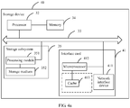
- FIG. 4a is a structural diagram of another storage device 40 according to an embodiment of the present invention.
- an interface card 41 in the storage device 40 is a smart interface card, and the interface card 41 may be a network interface card (Network Interface Card, NIC) supporting an Ethernet (Ethernet) protocol, an interface card based on an InfiniBand protocol, or another interface card that can implement the Remote Direct Memory Access RDMA Protocol.
- NIC Network Interface Card
- the interface card 41 includes a network interface device 411, a microprocessor 412, and a cache 413, the microprocessor 412 is connected to the network interface device 411, and the cache 413 is connected to the microprocessor 412 by using a memory bus.
- the network interface device 411, the microprocessor 412, the processor 32, and the storage subsystem 35 are connected by using the communications bus 33.
- the memory 34 and the processor 32 are connected by using another memory bus.
- the storage device 40 stores information such as data or an instruction in the cache 413 of the interface card 41
- the storage device 40 stores the information such as data or an instruction in the cache 413 of the interface card 41 by using a cache control unit.
- the cache control unit is in the interface card 41 of the storage device 40, and the cache control unit in the storage device 40, the cache control unit in the host 20, and the cache control unit in the storage device 30 are different and mutually independent.
- the cache control unit in the interface card 41 of the storage device 40 is in the microprocessor 412 and is connected to the cache 413 of the interface card 41 by using the memory bus.
- the cache control unit in the interface card 41 of the storage device 40 is outside the microprocessor 412 and is separately connected to the cache 413 and the microprocessor 412 of the interface card 41.
- the cache control unit in the interface card 41 of the storage device 40 is connected to the cache 413 of the interface card 41 by using the memory bus.
- the network interface device 411 is configured to receive or send information, and is further configured to: send, to the microprocessor 412, information or an instruction that complies with the preset standard protocol specification, and send, to the processor 32, information or an instruction that complies with a protocol specification other than the preset standard protocol specification.
- the microprocessor 412 is configured to process the information or the instruction that is received from the network interface device 411 and that complies with the preset standard protocol specification.
- the microprocessor 412 may be any computing component such as a microcontroller, a programmable controller, or another processing chip.
- the cache 413 may include a high-speed RAM memory, and may further include a non-volatile memory (English: non-volatile memory), for example, at least one magnetic disk memory. It may be understood that the cache 413 may be any machine-readable medium capable of storing program code, such as a random-access memory (English: Random-Access Memory, RAM), a magnetic disk, a hard disk, a solid state disk (English: Solid State Disk, SSD), or a non-volatile memory.
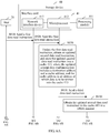
- the cache 413 is configured to store data, the instruction, or the information that is received by the microprocessor 412 and that complies with the preset standard protocol specification.
- the cache 413 is further configured to store at least one queue. For the queue stored in the cache 413, refer to the description of the queue in the memory 34 or a description of a queue in the cache 413 shown in FIG. 4b below.
- FIG. 4b is a schematic structural diagram of an interface card 41 in another storage device 40 according to an embodiment of the present invention. As shown in FIG. 4b , based on the interface card 41 shown in FIG. 4a , the interface card 41 further includes at least one interface 400 that is connected to the network interface device 411. In addition, different from the interface card 41 shown in FIG. 4a , in the interface card 41 shown in FIG. 4b , the cache 413 is integrated into the microprocessor 412.
- the interface 400 is configured to receive data, an instruction, or information that is sent by the interface card 21 of the host 20.
- the cache 413 shown in FIG. 4b is integrated into the microprocessor 412, and includes at least one submission queue 414 and at least one completion queue 415.
- the submission queue 414 is configured to store request information or an instruction that is sent by the host 20 and that is received by the network interface device 411.
- the completion queue 415 is configured to store a completion command that is sent by the storage subsystem 35 and that is received by the network interface device 411.
- functions of the submission queue 414 and the completion queue 415 refer to implementation of the functions of the submission queue and the completion queue in the memory 34 shown in FIG. 3 . Specific implementation details are not described herein again.
- a type of an access manner in which the host 20 accesses the storage device 40 is the same as a type of an access manner in which the host 20 accesses the storage device 30, and includes a data write access manner, a data read access manner, and an administrative command access manner.
- a method for sending a destination address and data to the interface card 41 of the storage device 40 by the host 20 in an RDMA manner is the same as an implementation in which the host 20 sends a destination address and data to the interface card 31 of the storage device 30 in an RDMA manner. Details are not described herein again.
- a sending manner of sending data, information, or an instruction to the interface card 41 of the storage device 40 by the host 20 is the same as a sending manner of sending information or an instruction to the interface card 31 of the storage device 30 by the host 20. Details are not described herein again.
- the cache 413 is a part of the memory 34, when the microprocessor 412 communicates with the cache 413, the microprocessor 412 needs to access the cache 413 in the memory 34 by using the cache control unit in the processor 32.
- the cache control unit in the processor 32 may alternatively be outside the processor 32.
- the cache control unit connected to the processor 32 refer to implementation details of the cache control unit in the processor 32 described based on FIG. 3 . A specific implementation is not described herein again.
- FIG. 5A and FIG. 5B are a flowchart of a data access method according to an unclaimed embodiment of the present invention. As shown in FIG.
- this unclaimed embodiment provides an access method for accessing the storage subsystem 35 by the host 20 in a data write access manner.
- step S510 is performed by the processor 22 of the host 20
- steps S520, S530, S540, and S580 are performed by the network interface device 411 of the interface card 41
- steps S550, S551, S570, and S571 are separately implemented by the microprocessor 412 of the interface card 41
- steps S560 to S564 are separately implemented by the processing module 351 of the storage subsystem 35.
- the data access method provided in this implementation specifically includes the following steps.
- the host 20 sends a first data write instruction to the interface card 41 of the storage device 40.
- the first data write instruction includes a destination address of data.
- the network interface device 411 of the interface card 41 obtains data and a destination address of the data.
- the network interface device 411 of the interface card 41 may obtain the data and the destination address of the data by using the first data write instruction, or may obtain the data and the destination address of the data in an RDMA manner.
- the first data write instruction includes the destination address of the data, and the first data write instruction is in an RDMA write access request.
- the host 20 sends data and a destination address of the data.
- the host 20 may send both the data and the destination address of the data to the interface card 41 of the storage device 40 by sending the first data write instruction.
- the first data write instruction includes the data and the destination address of the data.
- the network interface device 411 stores the data and the destination address of the data in the cache 413. Based on the interface card 41 shown in FIG. 4a and FIG. 4b , the network interface device 411 stores the data and the destination address of the data in the cache 413 of the interface card 41. The network interface device 411 sends the data to the cache control unit in the interface card 41, and the cache control unit in the interface card 41 stores the data in the cache 413. If the first data write instruction includes the destination address of the data, the network interface device 411 sends the destination address of the data to the microprocessor 412, and the microprocessor 412 of the interface card 41 stores the destination address of the data in the cache 413. The data may be sent to the network interface device 411 of the interface card 41 in the RDMA manner, and the network interface device 411 stores the data in the cache 413.
- the network interface device 411 sends the first data write instruction including the data and the destination address of the data to the microprocessor 412.
- the microprocessor 412 obtains the data and the destination address of the data after parsing the first data write instruction, and the microprocessor 42 of the interface card 41 stores the data in the cache 413.
- the network interface device 411 may store, in the cache 413, the data obtained after the first data write instruction is parsed, and send, to the microprocessor 412, the destination address of the data obtained after parsing is performed.
- the microprocessor 412 stores the destination address of the data in the cache 413.
- the cache control unit may be in the interface card 41, may be in the microprocessor 42, or may be outside the microprocessor 42 and connected to the microprocessor 42.
- the interface card 41 stores data or information in the cache 413 by using the cache control unit. If the network interface device 411 sends data or information to the cache 413, the network interface device 411 sends the data or the information to the cache control unit of the storage device 40, and the cache control unit of the storage device 40 stores the data or the information in the cache 413. If the microprocessor 412 sends data or information to the cache 413, the microprocessor 412 sends the data or the information to the cache control unit of the storage device 40, and the cache control unit of the storage device 40 stores the data or the information in the cache 413.
- the cache 413 is in the interface card 41, and the cache 413 of the interface card 41 stores the data, the destination address of the data, and a second data write instruction, so as to save a system memory resource of the storage device 40, and reduce a transmission delay.
- the network interface device 411 of the interface card 41 After receiving the first data write instruction, the network interface device 411 of the interface card 41 sends the first data write instruction to the microprocessor 412.
- the first data write instruction includes the destination address of the data.
- the microprocessor 412 updates the first data write instruction, obtains an updated second data write instruction, and stores the updated second data write instruction in the cache 413 of the interface card 41. Specifically, after updating the first data write instruction, the microprocessor 412 generates the second data write instruction.
- the updated second data write instruction includes a source address and the destination address of the data, and the source address is an address at which the data is stored in the cache 413.
- the microprocessor 412 stores the updated second data write instruction in the submission queue 414 of the cache 413 by using the cache control unit of the interface card 41.
- the cache control unit of the interface card 41 is connected to the cache 413 by using a memory bus, and the cache control unit is in the microprocessor 412 or outside the microprocessor 412.
- the microprocessor 412 updates the first data write instruction, obtains a second data write instruction, and stores the second data write instruction in the cache 413 of the memory 34. Specifically, the microprocessor 412 stores the updated second data write instruction in the submission queue 414 in the cache 413 of the memory 34 by using the cache control unit in the processor 34 or the cache control unit that is outside the processor 34 and that is connected to the memory 34 by using a memory bus.
- the microprocessor 412 of the interface card 41 sends a third data write instruction to the processing module 351.
- Sending of the third data write instruction to the processing module 351 aims to instruct the processing module 351 to obtain the updated second data write instruction in a DMA manner.
- the sent third data write instruction may be an address at which the updated second data write instruction is stored in the cache 413. If the updated second data write instruction is stored in the cache 413 in a form of a linked list, the third data write instruction sent by the microprocessor 412 may be a head address at which the updated second data write instruction is stored in the cache 413, that is, a head address of the linked list.
- the microprocessor 412 sends the address at which the updated second data write instruction is stored in the cache 413 to a register of the processing module 351, to instruct the processing module 351 to obtain, in the DMA manner according to the address at which the updated second data write instruction is stored in the cache 413, the stored updated second data write instruction from storage space to which the address at which the updated second data write instruction is stored in the cache 413 points.
- the processing module 351 obtains the updated second data write instruction from the submission queue 414 of the cache 413 in a DMA manner.
- an implementation in which the processing module 351 obtains the updated second data write instruction from the submission queue 414 of the cache 413 in the DMA manner is as follows: The processing module 351 obtains, in the DMA manner according to the address at which the updated second data write instruction is stored in the cache 413, the second data write instruction stored in the storage space to which the address at which the updated second data write instruction is stored in the cache 413 points.
- the processing module 351 sends a first obtaining instruction to the cache control unit of the interface card 41 by using a communications bus.
- the first obtaining instruction includes the address of the updated second data write instruction in the cache 413.
- the cache control unit of the interface card 41 sends, to the processing module 351, the updated second data write instruction stored in the submission queue of the cache 413.
- the cache control unit of the interface card 41 may be in the microprocessor 412, or may be connected to the microprocessor 412.
- the processing module 351 sends a first obtaining instruction to the cache control unit of the processor 34 by using a communications bus.
- the cache control unit may be outside the processor 34 and connected to the processor 34.
- the first obtaining instruction includes the address of the updated second data write instruction in the cache 413.
- the cache control unit After receiving the first obtaining instruction, the cache control unit sends, to the processing module 351, the updated second data write instruction stored in the submission queue of the cache 413.
- the second data write instruction is sent to the storage subsystem 35 in the direct memory access DMA manner, so as to improve efficiency of accessing the storage subsystem 35 in the storage device 40.
- the third data write instruction in step S551 is sent by the interface card 41 to the storage subsystem 35, and no resource of the processor 32 of the storage device 40 is used.
- the interface card 41 sends the third data write instruction in the present invention, so that no processing resource of the processor 32 of the storage device 40 is consumed, a processing rate for processing another event by the processor 32 of the storage device 40 is improved, and a rate for accessing the storage subsystem 35 of the storage device 40 by the host 20 is improved.
- the processing module 351 obtains the data from the cache 413 in the DMA manner. After the processing module 351 obtains the updated second data write instruction, the processing module 351 obtains the data from the cache 413 according to the source address of the data in the second data write instruction in the DMA manner. Specifically, the processing module 351 takes over the communications bus 33 from the processor 32, and controls the communications bus 33 to transmit, to the processing module 351, the data in storage space to which the source address in the cache 413 points.
- the processing module 351 sends a second obtaining instruction to the cache control unit of the interface card 41 by using the communications bus.
- the second obtaining instruction includes the source address in the updated second data write instruction.
- the cache control unit of the interface card 41 sends, to the processing module 351, the data stored in the storage space in the cache 413 to which the source address points.
- the processing module 351 sends a second obtaining instruction to the cache control unit of the processor 34 by using the communications bus.
- the cache control unit may be outside the processor 34 and connected to the processor 34.
- the second obtaining instruction includes the source address in the updated second data write instruction.
- the cache control unit After receiving the second obtaining instruction, the cache control unit sends, to the processing module 351, the data stored in the storage space in the cache 413 to which the source address points.
- the processing module 351 executes the second data write instruction, and writes the data into storage space in the storage medium 352 that is corresponding to the destination address.
- the processing module 351 executes the write instruction and writes the data into the storage space in the storage medium 352 that is corresponding to the destination address
- a specific implementation is not described herein again.
- the processing module 351 sends a completion command to a completion queue in the cache 413 in the DMA manner.
- the processing module 351 sends a completion request to the microprocessor 412.
- the microprocessor 412 After receiving the completion request, the microprocessor 412 obtains the completion command in the completion queue 415 according to a first in first out principle.
- the microprocessor 412 sends the completion command to the network interface device 411. S580.
- the network interface device 411 sends the completion command to the host 20.
- the interface card 41 In the method for accessing the storage device 40 in the data write access manner described in FIG. 5A and FIG. 5B , after the interface card 41 receives the first data write instruction, the interface card 41 generates the second data write instruction, and writes the second data write instruction into the cache 413. No resource of the processor 32 of the storage device 40 is used.
- the cache control unit in the microprocessor 412 of the interface card 41 sends the second data write instruction to the storage subsystem 35 to instruct the storage subsystem 35 to execute the second data write instruction.
- the updated second data write instruction further includes description information of the data, and the description information of the data includes description information such as a length of the data, an access type of the data, and an access priority of the data.
- the description information of the data includes description information such as a length of the data, an access type of the data, and an access priority of the data.
- the host 20 sends the description information of the data by sending the first data write instruction. After receiving the first data write instruction by using the microprocessor 412, the storage device 40 updates the first data write instruction. In another implementation, the host 20 may send RDMA write access information including the description information of the data to the interface card 41 in the RDMA manner. After receiving the description information of the data, the network interface device 411 of the interface card 41 directly stores the description information of the data in the cache 413. All information in the description information of the data, the data, and the destination address of the data may be encapsulated in one piece of RDMA write access information, or a part or all of the description information of the data may be encapsulated in a plurality of pieces of RDMA write access information.
- a part of the description information of the data may be included in the first data write instruction and sent to the storage device 40.
- a specific manner of sending the description information of the data is not limited in this embodiment. If the description information of the data is sent in the RDMA manner, the description information of the data needs to be sent to the interface card 41 before the first data write instruction is sent, so as to store the description information of the data in the cache 413.
- FIG. 6A and FIG. 6B are a flowchart of another data access method according to an embodiment of the present invention.
- this embodiment provides an access method for accessing the storage subsystem 35 by the host 20 in a data read access manner, and an access manner of reading, by the host 20 after data is written into the storage subsystem 35 of the storage device 40 in the implementation shown in FIG. 5A and FIG. 5B , the data stored in the storage subsystem 35 is mainly described.
- step S610 is performed by the processor 22 of the host 20
- steps S620 and S670 are separately implemented by the network interface device 411 of the interface card 41 of the storage device 40
- steps S630, S631, S650, and step S651 are separately implemented by the microprocessor 412 of the interface card 41 of the storage device 40
- steps S640 to S643 are separately implemented by the processing module 351 of the storage device 40.
- the data access method provided in this implementation specifically includes the following steps.
- the host 20 sends a first data read instruction to the interface card 41 of the storage device 40, where the first data read instruction includes the destination address, and the destination address is used to indicate an address at which the data is written into the storage subsystem 35.
- the first data read instruction includes the destination address
- the destination address is used to indicate an address at which the data is written into the storage subsystem 35.
- the network interface device 411 of the interface card 41 After receiving the first data read instruction, the network interface device 411 of the interface card 41 sends the first data read instruction to the microprocessor 412 of the interface card 41.
- the microprocessor 412 of the interface card 41 updates the first data read instruction, obtains an updated second data read instruction, and stores the updated second data read instruction in the cache 413 of the interface card 41. Specifically, after updating the first data read instruction, the microprocessor 412 generates the second data read instruction.
- the updated second data read instruction includes the destination address and a cache address, and the cache address is an address at which the data is to be written into the cache 413.
- the microprocessor 412 stores the updated second data read instruction in the submission queue 414 of the cache 413 by using the cache control unit of the interface card 41.
- the cache control unit of the interface card 41 is connected to the cache 413 by using a memory bus, and the cache control unit is in the microprocessor 412 or outside the microprocessor 412.
- the microprocessor 412 updates the first data read instruction, obtains a second data read instruction, and stores the second data read instruction in the cache 413 of the memory 34. Specifically, the microprocessor 412 stores the updated second data read instruction in the submission queue 414 in the cache 413 of the memory 34 by using the cache control unit in the processor 34 or the cache control unit that is outside the processor 34 and that is connected to the memory 34 by using a memory bus.
- the microprocessor 412 of the interface card 41 sends a third data read instruction to the processing module 351.
- Sending of the third data read instruction to the processing module 351 aims to instruct the processing module 351 to obtain the updated second data read instruction in a DMA manner.
- the sent third data read instruction may be an address at which the updated second data read instruction is stored in the cache 413. If the updated second data read instruction is stored in the cache 413 in a form of a linked list, the third data read instruction sent by the microprocessor 412 may be a head address at which the updated second data read instruction is stored in the cache 413, that is, a head address of the linked list.
- the microprocessor 412 sends the address at which the updated second data read instruction is stored in the cache 413 to a register of the processing module 351, to instruct the processing module 351 to obtain, in the DMA manner according to the address at which the updated second data read instruction is stored in the cache 413, the stored updated second data read instruction from storage space to which the address at which the updated second data read instruction is stored in the cache 413 points.
- the processing module 351 obtains the updated second data read instruction in the cache 413 in a DMA manner.
- the second data read instruction stored in the storage space to which the address at which the updated second data read instruction is stored in the cache 413 points is obtained according to the address at which the updated second data read instruction is stored in the cache 413.
- the processing module 351 sends a third obtaining instruction to the cache control unit of the interface card 41 by using a communications bus.
- the third obtaining instruction includes the address of the updated second data read instruction in the cache 413.
- the cache control unit of the interface card 41 sends, to the processing module 351, the updated second data read instruction stored in the submission queue of the cache 413.
- the processing module 351 sends a third obtaining instruction to the cache control unit of the processor 34 by using a communications bus.
- the cache control unit may be outside the processor 34 and connected to the processor 34.
- the third obtaining instruction includes the address of the updated second data read instruction in the cache 413.
- the cache control unit sends, to the processing module 351, the updated second data read instruction stored in the submission queue of the cache 413.
- the second data read instruction is sent to the storage subsystem 35 in the direct memory access DMA manner, so as to improve efficiency of accessing the storage subsystem 35 in the storage device 40.
- the third data read instruction in step S631 is generated by the microprocessor 412 of the interface card 41 and sent to the storage subsystem 35, and no resource of the processor 32 of the storage device 40 is used.
- the interface card 41 sends the third data read instruction in this embodiment, so that no processing resource of the processor 32 of the storage device 40 is consumed, a processing rate for processing another event by the processor 32 of the storage device 40 is improved, and a rate for accessing the storage subsystem 35 of the storage device 40 by the host 20 is improved.
- the processing module 351 executes the updated second data read instruction, and writes, in the DMA manner into storage space to which a cache address points, the data to which the destination address points.
- the processing module 351 sends a DMA write request to the cache control unit by using the communications bus.
- the DMA write request includes the data and the cache address.
- the cache control unit After receiving the DMA write request, the cache control unit writes the data into the storage space to which the cache address points.
- the processing module 351 sends a DMA write request to the cache control unit of the processor 34 by using the communications bus.
- the cache control unit may be outside the processor 34 and connected to the processor 34.
- the DMA write request includes the data and the cache address. After receiving the DMA write request, the cache control unit writes the data into the storage space to which the cache address points.
- the processing module 351 sends a completion command to a completion queue in the cache 413 in the DMA manner.
- the processing module 351 sends a completion request to the microprocessor 412.
- the microprocessor 412 After receiving the completion request, the microprocessor 412 obtains the completion command in the completion queue 415 according to a first in first out principle.
- the microprocessor 412 sends the data to the network interface device 411 in an RDMA manner.
- the microprocessor 412 sends the data to the network interface device 411 in the RDMA manner.
- the processor 32 sends data to the interface card 31 in two manners, and the interface card 31 sends the data to the host 20 in the data read access manner in which the host 20 accesses the storage device 30 in the embodiment of the storage device 30 shown in FIG. 3 .
- a specific implementation is not described herein again. Different from the data read access manner in which the host 20 accesses the storage device 30 in the embodiment of the storage device 30 shown in FIG. 3 , the microprocessor 412 sends the data to the network interface device 411 in this implementation.
- the network interface device 411 sends the data to the host 20 in the RDMA manner.
- the network interface device sends the data to the host 20 in the RDMA manner
- a specific implementation is not described herein again.
- the interface card 41 In the method that is for accessing the storage device 40 in the data read access manner and shown in FIG. 6A and FIG. 6B , after the interface card 41 receives the first data read instruction, the interface card 41 generates the second data read instruction, and writes the second data read instruction into the cache 413. No resource of the processor 32 of the storage device 40 is used.
- the cache control unit in the microprocessor 412 of the network interface card 41 sends the second data read instruction to the storage subsystem 35 to instruct the storage subsystem 35 to execute the second data read instruction.
- the present invention further provides another data access manner that is specifically an administrative command access manner.
- a sent first data read instruction does not include a destination address of data.
- a generated second data read instruction does not include the destination address of the data either.
- the processing module 351 executes the updated second data read instruction, and sends, to the cache 413, the data generated after the second data read instruction is updated.
- details of an implementation of the data access method corresponding to the administrative command access manner are the same as those of an implementation of the method in the data read access manner. For this, refer to the details of the data read access manner shown in FIG. 6A and FIG. 6B . Details are not described herein again.
- FIG. 7 is a structural diagram of another interface card according to an unclaimed embodiment of the present invention.
- the interface card provided in this unclaimed embodiment is applied to a storage device.
- the storage device 40 further includes a cache control unit, a cache 413, and a storage subsystem 35.
- the interface card 70 provided in this unclaimed embodiment includes a receiving unit 71 and a processing unit 72.
- the receiving unit 71 is connected to the processing unit 72.
- the receiving unit 71 is configured to receive a first data write instruction sent by a host.
- a function that the receiving unit 71 receives the first data write instruction sent by the host may be implemented by a network interface device 411 in the storage device 40.
- a network interface device 411 in the storage device 40.
- the processing unit 72 is configured to: obtain data and a destination address of the data, write the data and the destination address into the cache 413, generate a second data write instruction, and write the second data write instruction into the cache 413.
- the destination address is used to indicate an address at which the data is to be written into the storage subsystem 35.
- the second data write instruction includes a source address and the destination address, and the source address is an address at which the data is stored in the cache 413.
- a function that the processing unit 72 obtains the data may be implemented by the network interface device 411 in the storage device 40, and a function that the processing unit 72 obtains the destination address of the data may be implemented by a microprocessor 412 in the storage device 40.
- a function that the processing unit 72 obtains the data and the destination address of the data refer to specific details of step S520 shown in FIG. 5A and FIG. 5B . Details are not described herein again.
- a function that the processing unit 72 stores the data into the cache 413 may be implemented by the cache control unit, and when the cache control unit is in the microprocessor 412, the function is implemented by the microprocessor 412.
- a function that the processing unit 72 stores the destination address into the cache 413 may be implemented by the microprocessor 412 in an interface card 41 in the storage device 40.
- a function that the processing unit 72 generates the second data write instruction and writes the second data write instruction into the cache 413 may be implemented by the microprocessor 412 in the interface card 41 in the storage device 40.
- the processing unit 72 generates the second data write instruction and writes the second data write instruction into the cache 413, refer to specific details of step S550 shown in FIG. 5A and FIG. 5B . Details are not described herein again.
- the second data write instruction is used to instruct the storage subsystem 35 to read the data from the cache 413 according to the source address, and write the data into storage space corresponding to the destination address.
- the second data write instruction in the cache 413 is sent by the cache control unit to the storage subsystem 35.
- the cache control unit is connected to the cache 413.
- the cache control unit is outside the interface card 41 or in the interface card 41.
- the cache control unit may be in the microprocessor 412 or connected to the microprocessor 412.
- the storage subsystem 35 reads the data from the cache 413 according to the source address, and writes the data into the storage space corresponding to the destination address.
- the storage subsystem 35 is implemented by a solid state disk
- the storage subsystem 35 reads the data from the cache 413 according to the source address
- a function that the storage subsystem 35 writes the data into the storage space corresponding to the destination address is implemented by a processing module 351 in the solid state disk.
- steps S561 and S562 shown in FIG. 5A and FIG. 5B Details are not described herein again.
- FIG. 8 is a structural diagram of another interface card 70 according to an unclaimed embodiment of the present invention.
- the cache 413 is in the interface card 70 and is connected to the processing unit 72.
- the cache control unit is in the interface card 70.
- the cache control unit may be integrated into the processing unit 72, or may be outside the processing unit 72.
- FIG. 9 is a structural diagram of another interface card 70 according to an unclaimed embodiment of the present invention.
- the cache 413 is in the processing unit 72
- the cache control unit is in the interface card 70.
- the cache control unit may be integrated into the processing unit 72, or may be outside the processing unit 72.
- FIG. 10 is a structural diagram of another interface card 70 according to an unclaimed embodiment of the present invention.
- the interface card 70 further includes a sending unit 73, and the sending unit 73 is connected to the processing unit 72.
- the processing unit 72 is further configured to: generate a third data write instruction after generating the second data write instruction, and send the third data write instruction to the sending unit 73.
- the third data write instruction is used to instruct the storage subsystem 35 to obtain the second data write instruction from the cache 413 in a direct memory access manner.
- the sending unit 73 is configured to send the third data write instruction to the storage subsystem 35.
- a function that the processing unit 72 generates the third data write instruction is implemented by the microprocessor 412 in the interface card 41 of the storage device 40.
- a function that the sending unit 73 sends the third data write instruction to the storage subsystem 35 is implemented by the microprocessor 412 in the interface card 41 of the storage device 40.
- the sending unit 73 and the processing unit 72 may be integrated together or implemented by using two apparatuses. A specific implementation is not limited in this unclaimed embodiment. In an optional implementation, all or some of the sending unit 73, the processing unit 72, and the receiving unit 71 may be in the microprocessor 412.
- the cache 413 includes at least one submission queue, and the processing unit 72 is further configured to write the second data write instruction into the submission queue.
- the processing unit 72 is further configured to write the second data write instruction into the submission queue.
- the receiving unit 71 is further configured to receive a first data read instruction sent by the host.
- the first data read instruction includes the destination address.
- a function that the receiving unit 71 receives the first data read instruction sent by the host may be implemented by the network interface device 411 in the storage device 40.
- the first data read instruction refer to specific details of step S610 shown in FIG. 6A and FIG. 6B . Details are not described herein again.
- the processing unit 72 is further configured to: generate a second data read instruction, and write the second data read instruction into the cache 413.
- the second data read instruction includes the destination address and a cache address, and the cache address is an address at which the data is to be written into the cache 413 from the storage subsystem 35.
- a function that the processing unit 72 generates the second data read instruction and writes the second data read instruction into the cache 413 may be implemented by the microprocessor 412 of the interface card 41 in the storage device 40.
- steps S620 and S630 shown in FIG. 6A and FIG. 6B Details are not described herein again.
- the second data read instruction in the cache 413 is sent by the cache control unit to the storage subsystem 35.
- the second data read instruction is used to instruct the storage subsystem 35 to read the data from the storage space corresponding to the destination address, and write the data into the cache 413 according to the cache address.
- the storage subsystem 35 reads the data from the storage space corresponding to the destination address, and writes the data into the cache 413 according to the cache address.
- the storage subsystem 35 is implemented by a solid state disk, and a function that the storage subsystem 35 reads the data from the storage space corresponding to the destination address and writes the data into the cache 413 according to the cache address is implemented by the processing module 351 in the solid state disk.
- a function that the storage subsystem 35 reads the data from the storage space corresponding to the destination address and writes the data into the cache 413 according to the cache address is implemented by the processing module 351 in the solid state disk.
- step S641 shown in FIG. 6A and FIG. 6B Details are not described herein again.
- the processing unit 72 is further configured to: read the data from the cache 413, and send the data to the host 20.
- a function that the processing unit 72 reads the data from the cache 413 and sends the data to the host is implemented by the microprocessor 412 in the interface card 41 of the storage device 40.
- the microprocessor 412 in the interface card 41 of the storage device 40.
- the processing unit 72 is further configured to generate a third data read instruction.
- the third data read instruction is used to instruct the storage subsystem 35 to obtain the second data read instruction from the cache 413 in the direct memory access manner.
- a function that the processing unit 72 generates the third data read instruction is implemented by the microprocessor 412 in the interface card 41 of the storage device 40.
- step S631 shown in FIG. 6A and FIG. 6B . Details are not described herein again.
- the sending unit 73 is further configured to send the third data read instruction to the storage subsystem 35.
- a function that the sending unit 73 sends the third data read instruction to the storage subsystem 35 is implemented by the microprocessor 412 in the interface card 41 of the storage device 40.
- step S631 shown in FIG. 6A and FIG. 6B Details are not described herein again.
- the receiving unit 71 is further configured to obtain the data from the first data write instruction.
- a function that the receiving unit 71 obtains the data from the first data write instruction is implemented by the network interface device 411 in the interface card 41 of the storage device 40.
- the processing unit 72 is further configured to obtain the data from the first data write instruction.
- the processing unit 72 is further configured to obtain the destination address from the first data write instruction.
- a function that the processing unit 71 obtains the data and the destination address of the data from the first data write instruction may be implemented by the microprocessor 412 of the interface card 41.
- the receiving unit 71 is further configured to receive, in a remote direct memory manner, the data sent by the host.
- a function that the receiving unit 71 receives, in the remote direct memory manner, the data sent by the host 20 is implemented by the network interface device 411 in the interface card 41 of the storage device 40.
- the processing unit 72 is configured to receive, in the remote direct memory manner, the data and the destination address of the data that are sent by the host.
- a function that the processing unit 72 receives, in the remote direct memory manner, the data and the destination address of the data that are sent by the host may be implemented by the cache control unit. If the cache control unit is in the microprocessor 412, this function is implemented by the microprocessor 412.
- the receiving unit 71 is further configured to obtain the destination address of the data from the first data write instruction.
- a function that the receiving unit 71 obtains the destination address of the data from the first data write instruction is implemented by the network interface device 411 in the interface card 41 of the storage device 40.
- the network interface device 411 in the interface card 41 of the storage device 40.
- the receiving unit 71 is further configured to receive, in a remote direct memory manner, the destination address of the data sent by the host.
- a function that the receiving unit 71 receives, in the remote direct memory manner, the destination address of the data sent by the host 20 is implemented by the network interface device 411 in the interface card 41 of the storage device 40.
- the network interface device 411 in the interface card 41 of the storage device 40.
- all or some of units constituting the interface card 70 may be in the interface card 70.
- an embodiment of the present invention further provides a computer readable storage medium.
- the computer readable storage medium stores an instruction. When run on a computer, the instruction causes the computer to perform the data access method in FIG. 5A and FIG. 5B or FIG. 6A and FIG. 6B or any possible implementations of a related data access method.
- the interface card after the interface card receives the first data write instruction or the first data read instruction, the interface card generates the second data write instruction or the second data read instruction, and writes the second data write instruction or the second data read instruction into the cache. No resource of the processor of the storage device is used.
- the cache control unit sends the second data write instruction or the second data read instruction to the storage subsystem, and no resource of the processor of the storage device is used. Alternatively, the cache control unit may instruct the storage subsystem to execute the second data write instruction or the second data read instruction.
- the foregoing storage medium includes any non-transitory (non-transitory) machine-readable medium capable of storing program code, such as a USB flash drive, a removable hard disk, a magnetic disk, an optical disc, a random-access memory (Random-Access Memory, RAM), a solid state disk (Solid State Disk, SSD), or a non-volatile memory (non-volatile memory).
- a USB flash drive a removable hard disk
- a magnetic disk such as a magnetic disk, an optical disc, a random-access memory (Random-Access Memory, RAM), a solid state disk (Solid State Disk, SSD), or a non-volatile memory (non-volatile memory).
- RAM Random-Access Memory
- SSD Solid State Disk
- non-volatile memory non-volatile memory
Landscapes
- Engineering & Computer Science (AREA)
- Theoretical Computer Science (AREA)
- Physics & Mathematics (AREA)
- General Engineering & Computer Science (AREA)
- General Physics & Mathematics (AREA)
- Human Computer Interaction (AREA)
- Memory System Of A Hierarchy Structure (AREA)
- Information Transfer Systems (AREA)
Claims (15)
- Procédé d'accès à des données, dans lequel le procédé est appliqué sur un dispositif de stockage, le dispositif de stockage comprend une unité de commande de mémoire cache, une carte d'interface, une mémoire cache, et un sous-système de stockage, et le procédé comprend :la réception, par la carte d'interface, d'une première instruction d'écriture de données envoyée par un hôte ;l'obtention, par la carte d'interface, de données et d'une adresse de destination des données, dans lequel l'adresse de destination est utilisée pour indiquer une adresse à laquelle les données doivent être écrites dans le sous-système de stockage ;l'écriture, par la carte d'interface, des données et de l'adresse de destination dans la mémoire cache ;la génération, par la carte d'interface, d'une seconde instruction d'écriture de données, et l'écriture de la seconde instruction d'écriture de données dans la mémoire cache, dans lequel la seconde instruction d'écriture de données comprend une adresse de source et l'adresse de destination, et l'adresse de source est une adresse à laquelle les données sont stockées dans la mémoire cache ;l'envoi, par l'unité de commande de mémoire cache, de la seconde instruction d'écriture de données dans la mémoire cache au sous-système de stockage ; etla lecture, par le sous-système de stockage, des données à partir de la mémoire cache selon l'adresse de source, et l'écriture des données dans un espace de stockage correspondant à l'adresse de destination.
- Procédé selon la revendication 1, dans lequel la carte d'interface comprend un microprocesseur, la mémoire cache est dans la carte d'interface et est connectée au microprocesseur, et l'unité de commande de mémoire cache est dans la carte d'interface ; ou
dans lequel la carte d'interface comprend un microprocesseur, la mémoire cache est dans le microprocesseur, et l'unité de commande de mémoire cache est dans la carte d'interface ; ou
le dispositif de stockage comprend en outre un processeur, la mémoire cache est connectée au processeur, et la mémoire cache est à l'extérieur de la carte d'interface. - Procédé selon la revendication 2, dans lequel, lorsque le dispositif de stockage comprend en outre un processeur, avant l'obtention, par la carte d'interface, de données et d'une adresse de destination des données, le procédé comprend en outre :
l'envoi, par le processeur, de l'adresse de destination à l'hôte. - Procédé selon l'une quelconque des revendications 1 à 3, dans lequel la mémoire cache comprend au moins une file d'attente de soumission, et l'écriture de la seconde instruction d'écriture de données dans la mémoire cache comprend : l'écriture de la seconde instruction d'écriture de données dans la file d'attente de soumission.
- Procédé selon l'une quelconque des revendications 1 à 4, comprenant en outre :la réception, par la carte d'interface, d'une première instruction de lecture de données envoyée par l'hôte, dans lequel la première instruction de lecture de données comprend l'adresse de destination ;la génération, par la carte d'interface, d'une seconde instruction de lecture de données, et l'écriture de la seconde instruction de lecture de données dans la mémoire cache, dans lequel la seconde instruction de lecture de données comprend l'adresse de destination et une adresse de mémoire cache, et l'adresse de mémoire cache est une adresse à laquelle les données doivent être écrites dans la mémoire cache à partir du sous-système de stockage ;l'envoi, par l'unité de commande de mémoire cache, de la seconde instruction de lecture de données dans la mémoire cache au sous-système de stockage ;la lecture, par le sous-système de stockage, des données à partir de l'espace de stockage correspondant à l'adresse de destination, et l'écriture des données dans la mémoire cache selon l'adresse de mémoire cache ; etla lecture, par la carte d'interface, des données à partir de la mémoire cache, et l'envoi des données à l'hôte.
- Procédé selon l'une quelconque des revendications 1 à 5, dans lequel l'obtention, par la carte d'interface, de données et d'une adresse de destination des données comprend :
l'obtention, par la carte d'interface, des données et de l'adresse de destination des données à partir de la première instruction d'écriture de données. - Procédé selon l'une quelconque des revendications 1 à 6, dans lequel l'obtention, par la carte d'interface, de données et d'une adresse de destination des données comprend :
la réception, par la carte d'interface par accès direct de mémoire à distance, des données et de l'adresse de destination des données qui sont envoyées par l'hôte. - Dispositif de stockage (40), dans lequel le dispositif de stockage (40) comprend une unité de commande de mémoire cache, une carte d'interface (41), une mémoire cache (413), et un sous-système de stockage (35), dans lequel la carte d'interface (41) est configurée pour : recevoir une première instruction d'écriture de données envoyée par un hôte ; obtenir des données et une adresse de destination des données, dans lequel l'adresse de destination est utilisée pour indiquer une adresse à laquelle les données doivent être écrites dans le sous-système de stockage (35) ; écrire les données et l'adresse de destination dans la mémoire cache (413) ; générer une seconde instruction d'écriture de données ; et écrire la seconde instruction d'écriture de données dans la mémoire cache (413), dans lequel la seconde instruction d'écriture de données comprend une adresse de source et l'adresse de destination, et l'adresse de source est une adresse à laquelle les données sont stockées dans la mémoire cache (413) ;
l'unité de commande de mémoire cache est configurée pour envoyer la seconde instruction d'écriture de données dans la mémoire cache (413) au sous-système de stockage (35) ; et
le sous-système de stockage (35) est configuré pour : lire les données à partir de la mémoire cache selon l'adresse de source, et écrire les données dans un espace de stockage correspondant à l'adresse de destination. - Dispositif de stockage (40) selon la revendication 8, dans lequel la carte d'interface (41) comprend un microprocesseur (412), la mémoire cache (413) est dans la carte d'interface (41) et est connectée au microprocesseur (412), et l'unité de commande de mémoire cache est dans la carte d'interface (41) et est connectée à la mémoire cache (413) ; ou
la carte d'interface (41) comprend un microprocesseur (412), la mémoire cache (413) est dans le microprocesseur (412), et l'unité de commande de mémoire cache est dans la carte d'interface (41) et est connectée à la mémoire cache (413) ; ou
le dispositif de stockage (40) comprend en outre un processeur (32), la mémoire cache (413) est connectée au processeur (32), la mémoire cache (413) est à l'extérieur de la carte d'interface (41), l'unité de commande de mémoire cache est à l'extérieur de la carte d'interface (41), et l'unité de commande de mémoire cache est connectée à la mémoire cache (413). - Dispositif de stockage (40) selon la revendication 9, dans lequel le processeur (32) est configuré pour envoyer l'adresse de destination à l'hôte lorsque le dispositif de stockage comprend en outre le processeur (32).
- Dispositif de stockage (40) selon l'une quelconque des revendications 8 à 10, dans lequel la mémoire cache (413) comprend au moins une file d'attente de soumission, et la carte d'interface (41) est en outre configurée pour écrire la seconde instruction d'écriture de données dans la file d'attente de soumission.
- Dispositif de stockage (40) selon l'une quelconque des revendications 8 à 11, dans lequel
la carte d'interface (41) est en outre configurée pour : recevoir une première instruction de lecture de données envoyée par l'hôte, dans lequel la première instruction de lecture de données comprend l'adresse de destination ; générer une seconde instruction de lecture de données ; et écrire la seconde instruction de lecture de données dans la mémoire cache (413), dans lequel la seconde instruction de lecture de données comprend l'adresse de destination et une adresse de mémoire cache, et l'adresse de mémoire cache est une adresse à laquelle les données doivent être écrites dans la mémoire cache à partir du sous-système de stockage (35) ;
l'unité de commande de mémoire cache est en outre configurée pour envoyer la seconde instruction de lecture de données dans la mémoire cache (413) au sous-système de stockage (35) ;
le sous-système de stockage (35) est en outre configuré pour : lire les données à partir de l'espace de stockage correspondant à l'adresse de destination, et écrire les données dans la mémoire cache (413) selon l'adresse de mémoire cache ; et
la carte d'interface (41) est en outre configurée pour : lire les données à partir de la mémoire cache (413), et envoyer les données à l'hôte. - Dispositif de stockage (40) selon l'une quelconque des revendications 8 à 12, dans lequel la carte d'interface (41) est en outre configurée pour obtenir les données et l'adresse de destination des données à partir de la première instruction d'écriture de données.
- Dispositif de stockage (40) selon l'une quelconque des revendications 8 à 13, dans lequel la carte d'interface (41) est en outre configurée pour recevoir, par accès direct de mémoire à distance, les données et l'adresse de destination des données qui sont envoyées par l'hôte.
- Support de stockage lisible par ordinateur, dans lequel le support de stockage lisible par ordinateur stocke des instructions qui font en sorte que le dispositif de stockage de l'une quelconque des revendications 8 à 14 exécute le procédé d'accès à des données selon l'une quelconque des revendications 1 à 7.
Applications Claiming Priority (1)
| Application Number | Priority Date | Filing Date | Title |
|---|---|---|---|
| PCT/CN2017/080639 WO2018188084A1 (fr) | 2017-04-14 | 2017-04-14 | Procédé et dispositif d'accès à des données |
Publications (3)
| Publication Number | Publication Date |
|---|---|
| EP3598313A1 EP3598313A1 (fr) | 2020-01-22 |
| EP3598313A4 EP3598313A4 (fr) | 2020-04-15 |
| EP3598313B1 true EP3598313B1 (fr) | 2021-06-30 |
Family
ID=63792115
Family Applications (1)
| Application Number | Title | Priority Date | Filing Date |
|---|---|---|---|
| EP17905787.2A Active EP3598313B1 (fr) | 2017-04-14 | 2017-04-14 | Procédé et dispositif d'accès à des données |
Country Status (4)
| Country | Link |
|---|---|
| US (1) | US11144465B2 (fr) |
| EP (1) | EP3598313B1 (fr) |
| CN (1) | CN110419034B (fr) |
| WO (1) | WO2018188084A1 (fr) |
Families Citing this family (10)
| Publication number | Priority date | Publication date | Assignee | Title |
|---|---|---|---|---|
| CN112579311B (zh) * | 2019-09-30 | 2023-11-10 | 华为技术有限公司 | 访问固态硬盘的方法及存储设备 |
| CN110908600B (zh) * | 2019-10-18 | 2021-07-20 | 华为技术有限公司 | 数据访问方法、装置和第一计算设备 |
| CN113971138A (zh) * | 2020-07-24 | 2022-01-25 | 华为技术有限公司 | 一种数据访问方法及相关设备 |
| CN114303137A (zh) * | 2020-08-07 | 2022-04-08 | 美光科技公司 | 使用主机存储器缓冲器的存储器叠加 |
| EP4209886A4 (fr) * | 2020-09-30 | 2024-02-14 | Huawei Technologies Co., Ltd. | Circuit, puce et dispositif électronique |
| CN114327247A (zh) * | 2020-09-30 | 2022-04-12 | 华为技术有限公司 | 电路、芯片和电子设备 |
| CN113422793B (zh) * | 2021-02-05 | 2024-06-21 | 阿里巴巴集团控股有限公司 | 数据传输方法、装置、电子设备及计算机存储介质 |
| CN113641604B (zh) * | 2021-07-16 | 2024-02-02 | 济南浪潮数据技术有限公司 | 一种数据传输方法及系统 |
| US20240289286A1 (en) * | 2021-09-26 | 2024-08-29 | Intel Corporation | A Concept for Providing Access to Remote Memory |
| US11960419B2 (en) | 2022-07-19 | 2024-04-16 | Samsung Electronics Co., Ltd. | Systems and methods for data prefetching for low latency data read from a remote server |
Family Cites Families (13)
| Publication number | Priority date | Publication date | Assignee | Title |
|---|---|---|---|---|
| US5420998A (en) * | 1992-04-10 | 1995-05-30 | Fujitsu Limited | Dual memory disk drive |
| EP1858227A1 (fr) * | 2006-05-16 | 2007-11-21 | THOMSON Licensing | Dispositif de stockage en réseau avec interfaces de données séparées pour contrôle et pour stockage |
| CN101079798A (zh) * | 2006-05-26 | 2007-11-28 | 华为技术有限公司 | 网络地址转换方法及实现访问控制列表的方法 |
| TWI468047B (zh) | 2008-04-25 | 2015-01-01 | Koninkl Philips Electronics Nv | 多頻道無線網路之媒介存取控制協定 |
| US8832354B2 (en) * | 2009-03-25 | 2014-09-09 | Apple Inc. | Use of host system resources by memory controller |
| US8984221B2 (en) * | 2011-10-18 | 2015-03-17 | Hitachi, Ltd. | Method for assigning storage area and computer system using the same |
| TWI459201B (zh) * | 2012-04-27 | 2014-11-01 | Toshiba Kk | Information processing device |
| US10353631B2 (en) * | 2013-07-23 | 2019-07-16 | Intel Corporation | Techniques for moving data between a network input/output device and a storage device |
| US9571125B2 (en) * | 2013-10-03 | 2017-02-14 | Futurewei Technologies, Inc. | Systems and methods of vector-DMA cache-XOR for MPCC erasure coding |
| US10248587B2 (en) * | 2013-11-08 | 2019-04-02 | Sandisk Technologies Llc | Reduced host data command processing |
| WO2015145680A1 (fr) * | 2014-03-27 | 2015-10-01 | 株式会社日立製作所 | Ordinateur de gestion et système informatique |
| US9588898B1 (en) * | 2015-06-02 | 2017-03-07 | Western Digital Technologies, Inc. | Fullness control for media-based cache operating in a steady state |
| CN104965798B (zh) * | 2015-06-10 | 2018-03-09 | 上海华为技术有限公司 | 一种数据处理方法、相关设备以及系统 |
-
2017
- 2017-04-14 CN CN201780088559.6A patent/CN110419034B/zh active Active
- 2017-04-14 EP EP17905787.2A patent/EP3598313B1/fr active Active
- 2017-04-14 WO PCT/CN2017/080639 patent/WO2018188084A1/fr unknown
-
2019
- 2019-10-10 US US16/598,755 patent/US11144465B2/en active Active
Non-Patent Citations (1)
| Title |
|---|
| None * |
Also Published As
| Publication number | Publication date |
|---|---|
| EP3598313A4 (fr) | 2020-04-15 |
| WO2018188084A1 (fr) | 2018-10-18 |
| EP3598313A1 (fr) | 2020-01-22 |
| US11144465B2 (en) | 2021-10-12 |
| CN110419034A (zh) | 2019-11-05 |
| CN110419034B (zh) | 2021-01-08 |
| US20200050551A1 (en) | 2020-02-13 |
Similar Documents
| Publication | Publication Date | Title |
|---|---|---|
| EP3598313B1 (fr) | Procédé et dispositif d'accès à des données | |
| US10423568B2 (en) | Apparatus and method for transferring data and commands in a memory management environment | |
| US9467512B2 (en) | Techniques for remote client access to a storage medium coupled with a server | |
| CN109582614B (zh) | 针对远程存储器访问的nvm express控制器 | |
| EP3147792A1 (fr) | Procédé d'accès à un dispositif de stockage nvme et dispositif de stockage nvme | |
| EP2889780B1 (fr) | Système de traitement de données et procédé de traitement de données | |
| CN107305534B (zh) | 同时进行内核模式访问和用户模式访问的方法 | |
| EP4220419B1 (fr) | Modification de pointeurs de liste de pages de région physique nvme et de pointeurs de données pour faciliter le routage de demandes de mémoire pcie | |
| EP3465450B1 (fr) | Amélioration du débit dans des environnements openfabrics | |
| CN107092835B (zh) | 一种虚拟存储盘的计算机数据加密装置及方法 | |
| US11095626B2 (en) | Secure in-line received network packet processing | |
| CN112579311B (zh) | 访问固态硬盘的方法及存储设备 | |
| US20100082872A1 (en) | Method and apparatus to obtain code data for usb device | |
| CN104731635A (zh) | 一种虚拟机访问控制方法,及虚拟机访问控制系统 | |
| US20200242040A1 (en) | Apparatus and Method of Optimizing Memory Transactions to Persistent Memory Using an Architectural Data Mover | |
| CN114925012A (zh) | 一种以太网帧的下发方法、上传方法及相关装置 | |
| US7930445B2 (en) | Computer system using remote I/O and I/O data transfer method | |
| CN106325377B (zh) | 外部设备扩展卡及输入输出外部设备的数据处理方法 | |
| JP5847013B2 (ja) | 計算機及び計算機における入出力制御方法 | |
| CN112732176A (zh) | 基于fpga的ssd访问方法及装置、存储系统及存储介质 | |
| US20120166606A1 (en) | Distributed file operation apparatus, distributed file operation method, and non-transitory computer-readable medium storing distributed file operation program | |
| US20240168876A1 (en) | Solving submission queue entry overflow using metadata or data pointers | |
| US20140379792A1 (en) | Information processing apparatus and recording medium | |
| CN109039392B (zh) | 一种蓝牙设备 | |
| US20220334734A1 (en) | Information processing system and memory system |
Legal Events
| Date | Code | Title | Description |
|---|---|---|---|
| STAA | Information on the status of an ep patent application or granted ep patent |
Free format text: STATUS: THE INTERNATIONAL PUBLICATION HAS BEEN MADE |
|
| PUAI | Public reference made under article 153(3) epc to a published international application that has entered the european phase |
Free format text: ORIGINAL CODE: 0009012 |
|
| STAA | Information on the status of an ep patent application or granted ep patent |
Free format text: STATUS: REQUEST FOR EXAMINATION WAS MADE |
|
| 17P | Request for examination filed |
Effective date: 20191014 |
|
| AK | Designated contracting states |
Kind code of ref document: A1 Designated state(s): AL AT BE BG CH CY CZ DE DK EE ES FI FR GB GR HR HU IE IS IT LI LT LU LV MC MK MT NL NO PL PT RO RS SE SI SK SM TR |
|
| AX | Request for extension of the european patent |
Extension state: BA ME |
|
| A4 | Supplementary search report drawn up and despatched |
Effective date: 20200312 |
|
| RIC1 | Information provided on ipc code assigned before grant |
Ipc: G06F 13/10 20060101ALI20200306BHEP Ipc: G06F 12/0868 20160101ALI20200306BHEP Ipc: G06F 12/0893 20160101ALI20200306BHEP Ipc: G06F 12/0804 20160101ALI20200306BHEP Ipc: G06F 13/16 20060101ALI20200306BHEP Ipc: G06F 12/0866 20160101ALI20200306BHEP Ipc: G06F 3/06 20060101ALI20200306BHEP Ipc: G06F 12/0802 20160101ALI20200306BHEP Ipc: G06F 13/28 20060101AFI20200306BHEP |
|
| DAV | Request for validation of the european patent (deleted) | ||
| DAX | Request for extension of the european patent (deleted) | ||
| GRAP | Despatch of communication of intention to grant a patent |
Free format text: ORIGINAL CODE: EPIDOSNIGR1 |
|
| STAA | Information on the status of an ep patent application or granted ep patent |
Free format text: STATUS: GRANT OF PATENT IS INTENDED |
|
| INTG | Intention to grant announced |
Effective date: 20201118 |
|
| GRAJ | Information related to disapproval of communication of intention to grant by the applicant or resumption of examination proceedings by the epo deleted |
Free format text: ORIGINAL CODE: EPIDOSDIGR1 |
|
| STAA | Information on the status of an ep patent application or granted ep patent |
Free format text: STATUS: REQUEST FOR EXAMINATION WAS MADE |
|
| INTC | Intention to grant announced (deleted) | ||
| GRAS | Grant fee paid |
Free format text: ORIGINAL CODE: EPIDOSNIGR3 |
|
| STAA | Information on the status of an ep patent application or granted ep patent |
Free format text: STATUS: GRANT OF PATENT IS INTENDED |
|
| GRAP | Despatch of communication of intention to grant a patent |
Free format text: ORIGINAL CODE: EPIDOSNIGR1 |
|
| GRAA | (expected) grant |
Free format text: ORIGINAL CODE: 0009210 |
|
| STAA | Information on the status of an ep patent application or granted ep patent |
Free format text: STATUS: THE PATENT HAS BEEN GRANTED |
|
| INTG | Intention to grant announced |
Effective date: 20210517 |
|
| AK | Designated contracting states |
Kind code of ref document: B1 Designated state(s): AL AT BE BG CH CY CZ DE DK EE ES FI FR GB GR HR HU IE IS IT LI LT LU LV MC MK MT NL NO PL PT RO RS SE SI SK SM TR |
|
| REG | Reference to a national code |
Ref country code: CH Ref legal event code: EP |
|
| REG | Reference to a national code |
Ref country code: AT Ref legal event code: REF Ref document number: 1406981 Country of ref document: AT Kind code of ref document: T Effective date: 20210715 |
|
| REG | Reference to a national code |
Ref country code: DE Ref legal event code: R096 Ref document number: 602017041471 Country of ref document: DE |
|
| REG | Reference to a national code |
Ref country code: IE Ref legal event code: FG4D |
|
| REG | Reference to a national code |
Ref country code: LT Ref legal event code: MG9D |
|
| PG25 | Lapsed in a contracting state [announced via postgrant information from national office to epo] |
Ref country code: FI Free format text: LAPSE BECAUSE OF FAILURE TO SUBMIT A TRANSLATION OF THE DESCRIPTION OR TO PAY THE FEE WITHIN THE PRESCRIBED TIME-LIMIT Effective date: 20210630 Ref country code: HR Free format text: LAPSE BECAUSE OF FAILURE TO SUBMIT A TRANSLATION OF THE DESCRIPTION OR TO PAY THE FEE WITHIN THE PRESCRIBED TIME-LIMIT Effective date: 20210630 Ref country code: BG Free format text: LAPSE BECAUSE OF FAILURE TO SUBMIT A TRANSLATION OF THE DESCRIPTION OR TO PAY THE FEE WITHIN THE PRESCRIBED TIME-LIMIT Effective date: 20210930 |
|
| REG | Reference to a national code |
Ref country code: NL Ref legal event code: MP Effective date: 20210630 |
|
| REG | Reference to a national code |
Ref country code: AT Ref legal event code: MK05 Ref document number: 1406981 Country of ref document: AT Kind code of ref document: T Effective date: 20210630 |
|
| PG25 | Lapsed in a contracting state [announced via postgrant information from national office to epo] |
Ref country code: GR Free format text: LAPSE BECAUSE OF FAILURE TO SUBMIT A TRANSLATION OF THE DESCRIPTION OR TO PAY THE FEE WITHIN THE PRESCRIBED TIME-LIMIT Effective date: 20211001 Ref country code: NO Free format text: LAPSE BECAUSE OF FAILURE TO SUBMIT A TRANSLATION OF THE DESCRIPTION OR TO PAY THE FEE WITHIN THE PRESCRIBED TIME-LIMIT Effective date: 20210930 Ref country code: LV Free format text: LAPSE BECAUSE OF FAILURE TO SUBMIT A TRANSLATION OF THE DESCRIPTION OR TO PAY THE FEE WITHIN THE PRESCRIBED TIME-LIMIT Effective date: 20210630 Ref country code: RS Free format text: LAPSE BECAUSE OF FAILURE TO SUBMIT A TRANSLATION OF THE DESCRIPTION OR TO PAY THE FEE WITHIN THE PRESCRIBED TIME-LIMIT Effective date: 20210630 Ref country code: SE Free format text: LAPSE BECAUSE OF FAILURE TO SUBMIT A TRANSLATION OF THE DESCRIPTION OR TO PAY THE FEE WITHIN THE PRESCRIBED TIME-LIMIT Effective date: 20210630 |
|
| PG25 | Lapsed in a contracting state [announced via postgrant information from national office to epo] |
Ref country code: CZ Free format text: LAPSE BECAUSE OF FAILURE TO SUBMIT A TRANSLATION OF THE DESCRIPTION OR TO PAY THE FEE WITHIN THE PRESCRIBED TIME-LIMIT Effective date: 20210630 Ref country code: AT Free format text: LAPSE BECAUSE OF FAILURE TO SUBMIT A TRANSLATION OF THE DESCRIPTION OR TO PAY THE FEE WITHIN THE PRESCRIBED TIME-LIMIT Effective date: 20210630 Ref country code: RO Free format text: LAPSE BECAUSE OF FAILURE TO SUBMIT A TRANSLATION OF THE DESCRIPTION OR TO PAY THE FEE WITHIN THE PRESCRIBED TIME-LIMIT Effective date: 20210630 Ref country code: NL Free format text: LAPSE BECAUSE OF FAILURE TO SUBMIT A TRANSLATION OF THE DESCRIPTION OR TO PAY THE FEE WITHIN THE PRESCRIBED TIME-LIMIT Effective date: 20210630 Ref country code: PT Free format text: LAPSE BECAUSE OF FAILURE TO SUBMIT A TRANSLATION OF THE DESCRIPTION OR TO PAY THE FEE WITHIN THE PRESCRIBED TIME-LIMIT Effective date: 20211102 Ref country code: ES Free format text: LAPSE BECAUSE OF FAILURE TO SUBMIT A TRANSLATION OF THE DESCRIPTION OR TO PAY THE FEE WITHIN THE PRESCRIBED TIME-LIMIT Effective date: 20210630 Ref country code: EE Free format text: LAPSE BECAUSE OF FAILURE TO SUBMIT A TRANSLATION OF THE DESCRIPTION OR TO PAY THE FEE WITHIN THE PRESCRIBED TIME-LIMIT Effective date: 20210630 Ref country code: SK Free format text: LAPSE BECAUSE OF FAILURE TO SUBMIT A TRANSLATION OF THE DESCRIPTION OR TO PAY THE FEE WITHIN THE PRESCRIBED TIME-LIMIT Effective date: 20210630 Ref country code: SM Free format text: LAPSE BECAUSE OF FAILURE TO SUBMIT A TRANSLATION OF THE DESCRIPTION OR TO PAY THE FEE WITHIN THE PRESCRIBED TIME-LIMIT Effective date: 20210630 |
|
| PG25 | Lapsed in a contracting state [announced via postgrant information from national office to epo] |
Ref country code: PL Free format text: LAPSE BECAUSE OF FAILURE TO SUBMIT A TRANSLATION OF THE DESCRIPTION OR TO PAY THE FEE WITHIN THE PRESCRIBED TIME-LIMIT Effective date: 20210630 |
|
| REG | Reference to a national code |
Ref country code: DE Ref legal event code: R097 Ref document number: 602017041471 Country of ref document: DE |
|
| PG25 | Lapsed in a contracting state [announced via postgrant information from national office to epo] |
Ref country code: DK Free format text: LAPSE BECAUSE OF FAILURE TO SUBMIT A TRANSLATION OF THE DESCRIPTION OR TO PAY THE FEE WITHIN THE PRESCRIBED TIME-LIMIT Effective date: 20210630 |
|
| PLBE | No opposition filed within time limit |
Free format text: ORIGINAL CODE: 0009261 |
|
| STAA | Information on the status of an ep patent application or granted ep patent |
Free format text: STATUS: NO OPPOSITION FILED WITHIN TIME LIMIT |
|
| PG25 | Lapsed in a contracting state [announced via postgrant information from national office to epo] |
Ref country code: AL Free format text: LAPSE BECAUSE OF FAILURE TO SUBMIT A TRANSLATION OF THE DESCRIPTION OR TO PAY THE FEE WITHIN THE PRESCRIBED TIME-LIMIT Effective date: 20210630 |
|
| 26N | No opposition filed |
Effective date: 20220331 |
|
| PG25 | Lapsed in a contracting state [announced via postgrant information from national office to epo] |
Ref country code: IT Free format text: LAPSE BECAUSE OF FAILURE TO SUBMIT A TRANSLATION OF THE DESCRIPTION OR TO PAY THE FEE WITHIN THE PRESCRIBED TIME-LIMIT Effective date: 20210630 |
|
| REG | Reference to a national code |
Ref country code: CH Ref legal event code: PL |
|
| REG | Reference to a national code |
Ref country code: BE Ref legal event code: MM Effective date: 20220430 |
|
| PG25 | Lapsed in a contracting state [announced via postgrant information from national office to epo] |
Ref country code: MC Free format text: LAPSE BECAUSE OF FAILURE TO SUBMIT A TRANSLATION OF THE DESCRIPTION OR TO PAY THE FEE WITHIN THE PRESCRIBED TIME-LIMIT Effective date: 20210630 Ref country code: LU Free format text: LAPSE BECAUSE OF NON-PAYMENT OF DUE FEES Effective date: 20220414 Ref country code: CH Free format text: LAPSE BECAUSE OF NON-PAYMENT OF DUE FEES Effective date: 20220430 Ref country code: LI Free format text: LAPSE BECAUSE OF NON-PAYMENT OF DUE FEES Effective date: 20220430 |
|
| PG25 | Lapsed in a contracting state [announced via postgrant information from national office to epo] |
Ref country code: BE Free format text: LAPSE BECAUSE OF NON-PAYMENT OF DUE FEES Effective date: 20220430 |
|
| PG25 | Lapsed in a contracting state [announced via postgrant information from national office to epo] |
Ref country code: LT Free format text: LAPSE BECAUSE OF FAILURE TO SUBMIT A TRANSLATION OF THE DESCRIPTION OR TO PAY THE FEE WITHIN THE PRESCRIBED TIME-LIMIT Effective date: 20210630 Ref country code: IE Free format text: LAPSE BECAUSE OF NON-PAYMENT OF DUE FEES Effective date: 20220414 |
|
| PG25 | Lapsed in a contracting state [announced via postgrant information from national office to epo] |
Ref country code: MK Free format text: LAPSE BECAUSE OF FAILURE TO SUBMIT A TRANSLATION OF THE DESCRIPTION OR TO PAY THE FEE WITHIN THE PRESCRIBED TIME-LIMIT Effective date: 20210630 Ref country code: CY Free format text: LAPSE BECAUSE OF FAILURE TO SUBMIT A TRANSLATION OF THE DESCRIPTION OR TO PAY THE FEE WITHIN THE PRESCRIBED TIME-LIMIT Effective date: 20210630 |
|
| PGFP | Annual fee paid to national office [announced via postgrant information from national office to epo] |
Ref country code: GB Payment date: 20240229 Year of fee payment: 8 |
|
| PG25 | Lapsed in a contracting state [announced via postgrant information from national office to epo] |
Ref country code: HU Free format text: LAPSE BECAUSE OF FAILURE TO SUBMIT A TRANSLATION OF THE DESCRIPTION OR TO PAY THE FEE WITHIN THE PRESCRIBED TIME-LIMIT; INVALID AB INITIO Effective date: 20170414 |
|
| PGFP | Annual fee paid to national office [announced via postgrant information from national office to epo] |
Ref country code: FR Payment date: 20240311 Year of fee payment: 8 |
|
| PGFP | Annual fee paid to national office [announced via postgrant information from national office to epo] |
Ref country code: DE Payment date: 20240306 Year of fee payment: 8 |