EP3595037A1 - Structure of connection among circuit body, bus bar and electronic element - Google Patents
Structure of connection among circuit body, bus bar and electronic element Download PDFInfo
- Publication number
- EP3595037A1 EP3595037A1 EP19184921.5A EP19184921A EP3595037A1 EP 3595037 A1 EP3595037 A1 EP 3595037A1 EP 19184921 A EP19184921 A EP 19184921A EP 3595037 A1 EP3595037 A1 EP 3595037A1
- Authority
- EP
- European Patent Office
- Prior art keywords
- bus bar
- circuit body
- main line
- portions
- electronic element
- Prior art date
- Legal status (The legal status is an assumption and is not a legal conclusion. Google has not performed a legal analysis and makes no representation as to the accuracy of the status listed.)
- Granted
Links
- 238000007789 sealing Methods 0.000 claims description 7
- 230000008878 coupling Effects 0.000 description 32
- 238000010168 coupling process Methods 0.000 description 32
- 238000005859 coupling reaction Methods 0.000 description 32
- 239000010410 layer Substances 0.000 description 31
- 230000004308 accommodation Effects 0.000 description 23
- 239000002184 metal Substances 0.000 description 20
- 229910052751 metal Inorganic materials 0.000 description 20
- 239000011347 resin Substances 0.000 description 13
- 229920005989 resin Polymers 0.000 description 13
- 230000004048 modification Effects 0.000 description 10
- 238000012986 modification Methods 0.000 description 10
- 230000001012 protector Effects 0.000 description 10
- 230000009467 reduction Effects 0.000 description 10
- 238000004519 manufacturing process Methods 0.000 description 9
- 230000001105 regulatory effect Effects 0.000 description 8
- 230000003014 reinforcing effect Effects 0.000 description 8
- 238000004382 potting Methods 0.000 description 6
- 230000008859 change Effects 0.000 description 5
- 238000005452 bending Methods 0.000 description 3
- 239000010949 copper Substances 0.000 description 3
- 239000000463 material Substances 0.000 description 3
- 238000005192 partition Methods 0.000 description 3
- 238000000926 separation method Methods 0.000 description 3
- RYGMFSIKBFXOCR-UHFFFAOYSA-N Copper Chemical compound [Cu] RYGMFSIKBFXOCR-UHFFFAOYSA-N 0.000 description 2
- 239000012790 adhesive layer Substances 0.000 description 2
- 230000000712 assembly Effects 0.000 description 2
- 238000000429 assembly Methods 0.000 description 2
- 210000000078 claw Anatomy 0.000 description 2
- 229910052802 copper Inorganic materials 0.000 description 2
- 238000001514 detection method Methods 0.000 description 2
- 230000000694 effects Effects 0.000 description 2
- 239000010408 film Substances 0.000 description 2
- 239000000155 melt Substances 0.000 description 2
- 229920001721 polyimide Polymers 0.000 description 2
- 229910000679 solder Inorganic materials 0.000 description 2
- 239000010409 thin film Substances 0.000 description 2
- 238000004078 waterproofing Methods 0.000 description 2
- 239000004642 Polyimide Substances 0.000 description 1
- 230000002411 adverse Effects 0.000 description 1
- 239000012141 concentrate Substances 0.000 description 1
- 239000004020 conductor Substances 0.000 description 1
- 239000000470 constituent Substances 0.000 description 1
- 230000002093 peripheral effect Effects 0.000 description 1
Images


Classifications
-
- H—ELECTRICITY
- H01—ELECTRIC ELEMENTS
- H01M—PROCESSES OR MEANS, e.g. BATTERIES, FOR THE DIRECT CONVERSION OF CHEMICAL ENERGY INTO ELECTRICAL ENERGY
- H01M50/00—Constructional details or processes of manufacture of the non-active parts of electrochemical cells other than fuel cells, e.g. hybrid cells
- H01M50/50—Current conducting connections for cells or batteries
- H01M50/531—Electrode connections inside a battery casing
-
- H—ELECTRICITY
- H02—GENERATION; CONVERSION OR DISTRIBUTION OF ELECTRIC POWER
- H02B—BOARDS, SUBSTATIONS OR SWITCHING ARRANGEMENTS FOR THE SUPPLY OR DISTRIBUTION OF ELECTRIC POWER
- H02B1/00—Frameworks, boards, panels, desks, casings; Details of substations or switching arrangements
- H02B1/20—Bus-bar or other wiring layouts, e.g. in cubicles, in switchyards
-
- H—ELECTRICITY
- H01—ELECTRIC ELEMENTS
- H01M—PROCESSES OR MEANS, e.g. BATTERIES, FOR THE DIRECT CONVERSION OF CHEMICAL ENERGY INTO ELECTRICAL ENERGY
- H01M10/00—Secondary cells; Manufacture thereof
- H01M10/42—Methods or arrangements for servicing or maintenance of secondary cells or secondary half-cells
- H01M10/425—Structural combination with electronic components, e.g. electronic circuits integrated to the outside of the casing
-
- H—ELECTRICITY
- H01—ELECTRIC ELEMENTS
- H01M—PROCESSES OR MEANS, e.g. BATTERIES, FOR THE DIRECT CONVERSION OF CHEMICAL ENERGY INTO ELECTRICAL ENERGY
- H01M10/00—Secondary cells; Manufacture thereof
- H01M10/42—Methods or arrangements for servicing or maintenance of secondary cells or secondary half-cells
- H01M10/48—Accumulators combined with arrangements for measuring, testing or indicating the condition of cells, e.g. the level or density of the electrolyte
- H01M10/482—Accumulators combined with arrangements for measuring, testing or indicating the condition of cells, e.g. the level or density of the electrolyte for several batteries or cells simultaneously or sequentially
-
- H—ELECTRICITY
- H01—ELECTRIC ELEMENTS
- H01M—PROCESSES OR MEANS, e.g. BATTERIES, FOR THE DIRECT CONVERSION OF CHEMICAL ENERGY INTO ELECTRICAL ENERGY
- H01M50/00—Constructional details or processes of manufacture of the non-active parts of electrochemical cells other than fuel cells, e.g. hybrid cells
- H01M50/20—Mountings; Secondary casings or frames; Racks, modules or packs; Suspension devices; Shock absorbers; Transport or carrying devices; Holders
- H01M50/258—Modular batteries; Casings provided with means for assembling
- H01M50/26—Assemblies sealed to each other in a non-detachable manner
-
- H—ELECTRICITY
- H01—ELECTRIC ELEMENTS
- H01M—PROCESSES OR MEANS, e.g. BATTERIES, FOR THE DIRECT CONVERSION OF CHEMICAL ENERGY INTO ELECTRICAL ENERGY
- H01M50/00—Constructional details or processes of manufacture of the non-active parts of electrochemical cells other than fuel cells, e.g. hybrid cells
- H01M50/50—Current conducting connections for cells or batteries
- H01M50/502—Interconnectors for connecting terminals of adjacent batteries; Interconnectors for connecting cells outside a battery casing
- H01M50/505—Interconnectors for connecting terminals of adjacent batteries; Interconnectors for connecting cells outside a battery casing comprising a single busbar
-
- H—ELECTRICITY
- H05—ELECTRIC TECHNIQUES NOT OTHERWISE PROVIDED FOR
- H05K—PRINTED CIRCUITS; CASINGS OR CONSTRUCTIONAL DETAILS OF ELECTRIC APPARATUS; MANUFACTURE OF ASSEMBLAGES OF ELECTRICAL COMPONENTS
- H05K1/00—Printed circuits
- H05K1/02—Details
- H05K1/0277—Bendability or stretchability details
-
- H—ELECTRICITY
- H01—ELECTRIC ELEMENTS
- H01M—PROCESSES OR MEANS, e.g. BATTERIES, FOR THE DIRECT CONVERSION OF CHEMICAL ENERGY INTO ELECTRICAL ENERGY
- H01M2200/00—Safety devices for primary or secondary batteries
- H01M2200/10—Temperature sensitive devices
- H01M2200/103—Fuse
-
- H—ELECTRICITY
- H01—ELECTRIC ELEMENTS
- H01M—PROCESSES OR MEANS, e.g. BATTERIES, FOR THE DIRECT CONVERSION OF CHEMICAL ENERGY INTO ELECTRICAL ENERGY
- H01M2220/00—Batteries for particular applications
- H01M2220/20—Batteries in motive systems, e.g. vehicle, ship, plane
-
- H—ELECTRICITY
- H01—ELECTRIC ELEMENTS
- H01M—PROCESSES OR MEANS, e.g. BATTERIES, FOR THE DIRECT CONVERSION OF CHEMICAL ENERGY INTO ELECTRICAL ENERGY
- H01M50/00—Constructional details or processes of manufacture of the non-active parts of electrochemical cells other than fuel cells, e.g. hybrid cells
- H01M50/20—Mountings; Secondary casings or frames; Racks, modules or packs; Suspension devices; Shock absorbers; Transport or carrying devices; Holders
- H01M50/204—Racks, modules or packs for multiple batteries or multiple cells
- H01M50/207—Racks, modules or packs for multiple batteries or multiple cells characterised by their shape
- H01M50/209—Racks, modules or packs for multiple batteries or multiple cells characterised by their shape adapted for prismatic or rectangular cells
-
- Y—GENERAL TAGGING OF NEW TECHNOLOGICAL DEVELOPMENTS; GENERAL TAGGING OF CROSS-SECTIONAL TECHNOLOGIES SPANNING OVER SEVERAL SECTIONS OF THE IPC; TECHNICAL SUBJECTS COVERED BY FORMER USPC CROSS-REFERENCE ART COLLECTIONS [XRACs] AND DIGESTS
- Y02—TECHNOLOGIES OR APPLICATIONS FOR MITIGATION OR ADAPTATION AGAINST CLIMATE CHANGE
- Y02E—REDUCTION OF GREENHOUSE GAS [GHG] EMISSIONS, RELATED TO ENERGY GENERATION, TRANSMISSION OR DISTRIBUTION
- Y02E60/00—Enabling technologies; Technologies with a potential or indirect contribution to GHG emissions mitigation
- Y02E60/10—Energy storage using batteries
Landscapes
- Chemical & Material Sciences (AREA)
- Chemical Kinetics & Catalysis (AREA)
- Electrochemistry (AREA)
- General Chemical & Material Sciences (AREA)
- Engineering & Computer Science (AREA)
- Manufacturing & Machinery (AREA)
- Microelectronics & Electronic Packaging (AREA)
- Power Engineering (AREA)
- Connection Of Batteries Or Terminals (AREA)
Abstract
Description
- The present invention relates to a structure of connection among a circuit body, a bus bar and an electronic element.
- Conventionally, a flexible board (FPC: Flexible Printed Circuits) where a wiring pattern is provided has been used as wiring that connects between various electronic devices (for example, see
JP-A-2002-093995 - The present invention relates to a structure of connection among a circuit body, a bus bar and an electronic element, and a bus bar module using the connection structure.
- Conventionally, a flexible board (FPC: Flexible Printed Circuits) where a wiring pattern is provided has been used as wiring that connects between various electronic devices (for example, see
JP-A-2002-093995 - When an electronic element is directly mounted on a flexible board, normally, a reinforcing plate that is more difficult to become deformed than the constituent material (for example, a polyimide film) of the flexible board is provided on the mounting area of the electronic element in order that separation of the portion of connection between the wiring pattern and the electronic element (for example, a soldered portion) or the like does not occur due to a deformation of the flexible board. However, the provision of the reinforcing plate is undesirable from the viewpoint of reduction in the size of the flexible board, reduction in the number of parts and the like. Accordingly, it is desired to suppress deformation of the flexible board in the mounting area of the electronic element without the use of a reinforcing plate.
- The present invention is made in view of the above-mentioned circumstances, and an object thereof is to provide a structure of connection between a circuit body, a bus bar and an electronic element capable of suppressing deformation of the flexible board in the mounting area of the electronic element.
- To attain the above-mentioned object, a structure of connection among a circuit body, a bus bar and an electronic element according to the present invention and a bus bar module according to the present invention are characterized by the following [1] to [5]:
- [1] The structure of connection among a circuit body, a bus bar and an electronic element, the connection structure being provided with:
- a circuit body configured by a flexible board on which a wiring pattern is provided;
- a bus bar attached to a mounting surface of the circuit body; and
- an electronic element attached to the mounting surface so as to connect the bus bar and the wiring pattern,
- wherein the bus bar has a fixed portion extending along the mounting surface;
- wherein the fixed portion is fixed to the mounting surface so that a restricted area which restricts deformation of the mounting surface is formed in a periphery of the fixed portion; and
- wherein the electronic element is arranged in the restricted area and is fixed to the mounting surface.
- [2] In the connection structure according to the above [1],
the fixed portion of the bus bar has a first portion extending in a direction along the mounting surface and a pair of second portions extending in a direction intersecting with the first portion and along the mounting surface; and
the first portion and the pair of second portions are fixed to the mounting surface so that the restricted area is formed in a part sandwiched between the pair of second portions. - [3] In the connection structure according to the above [1] or [2],
the electronic element is attached to the mounting surface so as to connect the fixed portion and the wiring pattern. - [4] In the connection structure according to any one of the above [1] to [3],
the fixed portion is higher than the electronic element in a thickness direction of the circuit body; and
the connection structure further being provided with:
a sealing member that is arranged in the restricted area formed by the fixed portion and covers the electronic element so as to isolate the electronic element from an outside. - [5] A bus bar module attached to a battery assembly where a plurality of single cells are laminated, the bus bar module being provided with:
- a circuit body configured by a flexible board on which a wiring pattern is provided;
- a bus bar configured to be connected to an electrode of each of the single cells; and
- a holder configured to hold the bus bar and being stretchable and shrinkable in the first direction,
- wherein the circuit body includes:
- a belt-like main line that extends in the first direction;
- a belt-like branch line that extends from the main line so as to branch from the main line, a part of the branch line extending in the first direction and including a folded portion having a shape folded back around an axis intersecting with the first direction;
- a connection portion provided in a position closer to a distal end of the branch line than the folded portion and configured to be connected to the bus bar; and
- an electronic element attached to a mounting surface of the connection portion so as to connect the bus bar and the wiring pattern,
- wherein at the connection portion, the circuit body, the bus bar and the electronic element are connected by the connection structure according to any one of the above [1] to [4].
- According to the connection structure of the structure of the above [1], the bus bar originally used for electric connection with an external device or the like is used, and the restricted area where deformation of the circuit body is regulated is formed within the mounting surface of the circuit body. For example, if a fixed portion of a form surrounding a specific area is fixed to the mounting surface, the circuit body in the restricted area is in a stretched condition by being supported by the fixed portion. Consequently, even if an external force reaches the circuit body, the circuit body in the restricted area surrounded by the fixed portion is kept in a flat condition and cannot be easily deformed. And the electric element is mounted in the restricted area where deformation is regulated as described above. Thereby, deformation of the circuit body in the mounting area of the electronic element can be regulated without the use of an attached member such as a conventionally used reinforcing plate. In other words, deformation of the flexible board in the mounting area of the electronic element can be appropriately suppressed while reduction in the size of the flexible board and reduction in the number of parts are attained. The above-mentioned "deformation" is a concept including various deformation modes that can affect the condition of attachment of the electronic element to the mounting surface such as curving and flexion of the circuit body in the thickness direction of the circuit body, twisting of the circuit body and bending of the circuit body.
- According to the connection structure of the structure of the above [2], by the first portion and the pair of second portions, the fixed portion can be structured that has, for example, a form surrounding a specific area from three sides so that one side is open (as an example, a substantial U shape). At this time, if the electronic element is mounted in the area sandwiched between the pair of second portions, not only separation of the electronic element or the like can be suppressed by regulating deformation of the circuit body but also the wiring pattern connecting with the electronic element can be easily provided through the part having no fixed portion and being open. That is, the connection structure of the present structure can provide a fixed portion of a form excellent in practicality.
- According to the connection structure of the structure of the above [3], the fixed portion of the bus bar can be used as the point of contact between the bus bar and the electronic element. Therefore, contribution to reduction in the size and reduction in the cost of the connection structure can be made more than in a case where the point of contact between the bus bar and the electronic element is provided in another portion different from the fixed portion.
- According to the connection structure of the structure of the above [4], by the sealing member covering the electronic element (for example, a potting material), the waterproofing property of, for example, the electronic element and the point of contact between the electronic element and the bus bar can be enhanced. Further, if the sealing member is fixed in a state of adhering to the mounting surface, an external force is restrained from reaching the point of contact between the electronic element and the bus bar by the sealing member, so that deformation of the circuit body is further solidly suppressed. From this point of view, it is preferable that the sealing member be provided so as to fill the entire part of the area formed by the fixed portion of the bus bar.
- According to the bus bar module of the structure of the above [5], the folded portion is configured so that the connection portion and the main line are along surfaces different in the thickness direction of the main line. For this reason, when the bus bar module is assembled to the battery assembly, the lower surface of the main line is situated away from the upper surfaces of the single cells. Therefore, for example, it is unnecessary to provide a protecting member or the like for protecting the circuit body between the main line of the circuit body and the upper surfaces of the single cells, so that contribution can be made to reduction in height, reduction in the number of parts, simplification of the manufacturing process and the like of the bus bar module. At this time, if the main line and the branch line have a strength of a degree that can maintain the condition where the main line of the circuit body is away from the upper surfaces of the single cells, the circuit body is self-standing. Moreover, a support member for maintaining such a condition may be used as required. That is, the circuit body may be configured so as to be self-standing to maintain the above-mentioned condition, or may be configured so as to maintain the above-mentioned condition by using a different member or the like.
- Further, according to the bus bar module of the above-described structure, the bus bar originally used for electric connection with the single cells is used, and the area where deformation of the circuit body is regulated is formed within the mounting surface of the connection portion. For example, if a bus bar of a form surrounding a specific area is fixed to the mounting surface (specifically, the fixed portion), the circuit body in the area is in a stretched condition by being supported by the fixed portion. Consequently, even if an external force reaches the circuit body, the circuit body in the area surrounded by the fixed portion is kept in a flat condition and cannot be easily deformed. And the electric element is mounted in the area where deformation is regulated as described above. Thereby, deformation of the circuit body in the mounting area of the electronic element can be regulated without the use of an attached member such as a conventionally used reinforcing plate.
- As described above, the bus bar module of the present structure is excellent in the assemblability to the battery assembly and the conformability to the deformation of the battery assembly and the manufacturing variations compared with general bus bar modules. Further, the bus bar module of the present structure is capable of appropriately suppressing the deformation of the flexible board in the mounting area of the electronic element while reducing the size and the number of parts of the flexible board particularly at the portion of connection with the bus bar.
- According to the present invention, a structure of connection among a circuit body, a bus bar and an electronic element capable of suppressing the deformation of a flexible board in a mounting area of the electronic element, and a bus bar module can be provided.
- The present invention has been briefly described above. Further, details of the present invention will be further clarified by reading through the mode for carrying out the invention (hereinafter, referred to as "embodiment") described below with reference to the attached drawings.
-
-
FIG. 1 is an overall perspective view of a bus bar module according to the present embodiment. -
FIG. 2 is a perspective view of a battery assembly to which the bus bar module to which the present invention is applied is assembled. -
FIG. 3 is a perspective view where an end portion of a circuit body is enlarged. -
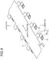
FIG. 4 is a perspective view showing the structure of a main line, first branch portions and second branch portions constituting the circuit body. -
FIG. 5A is a perspective view showing a condition where the second branch portion is bent in an S shape as a whole,FIG. 5B is a perspective view showing a shape into which the second branch portion is deformed when the bus bar relatively moves rearward, andFIG. 5C is a perspective view of a condition where the bus bar relative moves forward so that the second branch portion stretches. -
FIG. 6 is a perspective view showing a part of the holder. -
FIG. 7 is a perspective view of an accommodation space in a bus bar accommodating portion. -
FIGS. 8A to 8C are perspective views showing modifications of a folded portion of the second branch portion constituting the circuit body;FIG. 8A shows a case where the folded portion is Z-shaped as a whole,FIG. 8B shows a case where the folded portion is C-shaped as a whole, andFIG. 8C shows a case where the folded portion is O-shaped as a whole. -
FIG. 9A is a perspective view showing a modification of the first branch portion, andFIG. 9B is a perspective view showing a modification of a position of branch of the main line and the branch line. -
FIG. 10 is a perspective view where the periphery of the position of contact between a connection piece of the bus bar and a connection portion of the second branch portion is enlarged. -
FIG. 11A is a top view of the periphery of the connection position shown inFIG. 10 , andFIG. 11B is an A-A cross-sectional view ofFIG. 11A . -
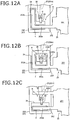
FIG. 12A is a view, corresponding toFIG. 11A , of the bus bar module according to a modification of the present embodiment,FIG. 12B is a view, corresponding toFIG. 11A , of the bus bar module according to another modification of the present embodiment, andFIG. 12C is a view, corresponding toFIG. 11A , of the bus bar module according to still another modification of the present embodiment. -
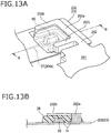
FIG. 13A is a perspective view where the periphery of the position of connection between the connection piece of the bus bar and the connection portion of the second branch portion on the bus bar module according to another modification of the present embodiment is enlarged, andFIG. 13B is a B-B cross-sectional view ofFIG. 13A . -
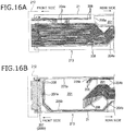
FIG. 14A is a cross-sectional view corresponding to an upper side metal layer on a part of the circuit body, andFIG. 14B is a cross-sectional view corresponding to a lower side metal layer on part of the circuit body. -
FIG. 15 is a cross-sectional view where the periphery of one branch portion on the circuit body shown inFIG. 14A is enlarged. -
FIG. 16A is a cross-sectional view corresponding to the upper side metal layer in the periphery of the front end portion of the circuit body, andFIG. 16B is a cross-sectional view corresponding to the lower side metal layer in the periphery of the front end portion of the circuit body. -
FIG. 17 is a cross-sectional view corresponding toFIG. 16B at the front end portion of the circuit body according to another modification of the present embodiment. -
FIG. 18A is a perspective view showing a manner in which a cover is attached to the holder of the bus bar module, andFIG. 18B is a perspective view showing the condition where the cover is attached to the holder of the bus bar module. -
FIG. 19 is a side view for explaining the position of engagement between the holder and the cover. -
FIG. 20A is a perspective view of a cover in the assembled condition, andFIG. 20B is an exploded perspective view of the cover. -
FIG. 21A is an upper view of the cover in the assembled condition,FIG. 21B is a cross-sectional view corresponding to the C-C cross section ofFIG. 21A on the cover in the most stretched condition, andFIG. 21C is a cross-sectional view corresponding to the C-C cross section ofFIG. 21A in the most shrunken condition. -
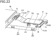
FIG. 22 is a perspective view showing the condition where a protector attached to the circuit body exposed from the cover is fixed to the cover. -
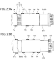
FIG. 23A is an upper view of the protector attached to the circuit body exposed from the cover, andFIG. 23B is a lower view of the protector attached to the circuit body exposed from the cover. -
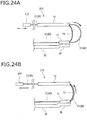
FIG. 24A is a schematic view for explaining a manner in which a connector provided on the front end portion of the circuit body moves forward under the condition where the protector is fixed to the cover, andFIG. 24B is a schematic view for explaining a manner in which the connector provided on the front end portion of the circuit body moves rearward under the condition where the protector is fixed to the cover. - Hereinafter, referring to the drawings, a
bus bar module 10 using a structure of connection among a circuit body, a bus bar and an electronic element according to an embodiment of the present invention will be described. Thebus bar module 10 according to the present embodiment is used in such a manner as to be assembled to a battery assembly (a battery module where a plurality of single cells are disposed so as to be assembled) as a driving power source mounted on, for example, an electric car and a hybrid car. - First, a
battery assembly 1 to which thebus bar module 10 of the present embodiment is attached will be described. As shown inFIG. 2 , thebattery assembly 1 is formed by linearly connecting a plurality of single cells 2. The single cells 2 each have apositive electrode 4 and anegative electrode 5 provided so as to project on the top portion of a battery body (body) 3 formed in a rectangular shape. Thepositive electrode 4 and thenegative electrode 5 are disposed away from each other on anelectrode surface 6 of thebattery body 3, and are each provided so as to substantially vertically project upward from theelectrode surface 6 in a cylindrical shape. - In the
battery assembly 1, the single cells 2 are arranged so as to be assembled in a predetermined direction (assembled direction) in such a manner that thepositive electrodes 4 and thenegative electrodes 5 of the adjoining single cells 2 alternate with each other. In thisbattery assembly 1, for example, thepositive electrode 4 of one of the single cells 2 corresponding to both ends of the series-connected single cells 2 is the total positive electrode, whereas thenegative electrode 5 of the other of the single cells 2 is the total negative electrode. - Next, the bus bar module of the present embodiment will be described. As shown in
FIG. 1 , thebus bar module 10 has: acircuit body 20 formed of a flexible board (FPC) and to which bus bars 25 (seeFIG. 3 ) connected to thepositive electrodes 4 and thenegative electrodes 5 of the single cells 2 are attached; and a holder (wire routing member) 30 for accommodating and holding thecircuit body 20 and for the attachment to thebattery assembly 1. - As shown in
FIGS. 1 and3 , thecircuit body 20 has a belt-likemain line 21 disposed in the assembled direction on the single cells 2 and where a plurality of wiring patterns (details will be described later) are provided. To an end portion of themain line 21, aconnector 212 is attached through avoltage detection line 211 pulled out from themain line 21. Theconnector 212 is connectable to a later-described voltage detector 60 (seeFIG. 22 ). - On the side portions of the
main line 21 in the length direction (in the present example, substantially coinciding with the "assembled direction" of the battery assembly 1), belt-likefirst branch portions 22 extending in a direction intersecting with the length direction and thickness direction of the main line 21 (outside of themain line 21 in the width direction) are provided, and at the leading end of eachfirst branch portion 22, a belt-likesecond branch portion 23 extending in a direction parallel to the assembled direction of thebattery bodies 3 is provided. Themain line 21, thefirst branch portions 22 and thesecond branch portions 23 are formed of an FPC. Therefore, themain line 21, thefirst branch portions 22 and thesecond branch portions 23 are flexibly deformable particularly in a direction orthogonal to the surface of each. - As shown in
FIGS. 4 and5A , thesecond branch portions 23 each have a foldedportion 231 folded back around axes L1 and L2 (in other words, around axes extending in the width direction of the second branch portion 23) intersecting with the assembled direction of the battery assembly 1 (in the present example, substantially coinciding with the extension direction of the second branch portion 23). In the present example, thesecond branch portions 23 are each bent in an S shape (including an inverted S shape) as a whole by a first foldedportion 231A folded back with respect to the axis L1 and a second foldedportion 231B folded back with respect to the axis L2. For this reason, thesecond branch portion 23 is movable in the length direction of the main line 21 (the assembled direction of the battery assembly 1) and stretchable and shrinkable also in the vertical direction. - The
first branch portion 22 is provided so as to be flush with themain line 21 outside themain line 21, and thesecond branch portion 23 is connected to thefirst branch portion 22. For this reason, thesecond branch portion 23 is provided outside themain line 21 in the width direction, and is provided so as to be S-shaped downward under the condition where the relative positions of thebattery assembly 1 and thecircuit body 20 do not change (seeFIG. 5A ). For this reason, thebus bar 25 is situated below the plane of themain line 21 outside themain line 21 in the width direction. - Moreover, on the end portion of the
second branch portion 23 opposite to thefirst branch portion 22, aleading end portion 232 having a surface substantially parallel to themain line 21 is provided, and to the upper surface of theleading end portion 232, aconnection portion 24 is attached. The lower surface of theconnection portion 24 is provided parallel to the lower surface of themain line 21 in a different height position, and the lower surfaces are away from each other. The upper surface of theconnection portion 24 is connected to thebus bar 25 connecting thepositive electrode 4 and thenegative electrode 5 of the adjoining single cells 2 in thebattery assembly 1. Thereby, thesecond branch portion 23 is connected to the electrodes of each single cell 2 through theconnection portion 24 and thebus bar 25, so that thevoltage detection line 211 is connected to the electrodes. - As shown in
FIGS. 3 and5A to 5C , thebus bar 25 has: abus bar body 251 which is a plate-like member formed of a conductor (for example, made of copper) and is rectangular as a whole; and aconnection piece 252 projecting from thebus bar body 251 toward themain line 21. Thebus bar body 251 is provided with twoelectrode holes 253 through which thepositive electrode 4 and thenegative electrode 5 of the adjoining single cells 2 are passed. At the end portion on the side of themain line 21 and the end portion on the opposite side on thebus bar body 251, positioningconcave portions 254 are provided so as to correspond to intervals between the two electrode holes 253. Moreover, to the lower surface of theconnection piece 252 of thebus bar body 251, theconnection portion 24 of thesecond branch portion 23 is connected. A concrete form of the connection between theconnection piece 252 of thebus bar 25 and theconnection portion 24 of thesecond branch portion 23 will be described later. - A
bus bar 25A provided on each end of themain line 21 in the length direction is connected to the total positive electrode or the total negative electrode, and is provided with oneelectrode hole 253 through which the total positive electrode or the total negative electrode is passed. To thebus bar 25A, a power cable (not shown) that derives power from thebattery assembly 1 is connected. The internal structure of themain line 21, thefirst branch portions 22 and thesecond branch portions 23 constituting thecircuit body 20 will be described later. - As shown in
FIG. 6 , theholder 30 is formed of, for example, resin, and has, in a central portion in the width direction, a mainline accommodating portion 31 extending in the assembled direction of the single cells 2 and accommodating and holding themain line 21. The mainline accommodating portion 31 is provided with mainline support members 311 at predetermined intervals in the length direction of themain line 21 that it accommodates, and themain line 21 is routed on the mainline support members 311. When themain line 21, thefirst branch portions 22 and thesecond branch portions 23 have a strength of a degree capable of maintaining a condition where thecircuit body 20 of the present example is self-standing without the support by the mainline support members 311, it is unnecessary to provide the mainline support members 311. However, even in this case, the mainline support members 311 may be provided in order to deliver an auxiliary support function when thecircuit body 20 cannot maintain the self-standing condition for some reason. As described above, thecircuit body 20 may be configured so as to maintain the above-mentioned condition by using the mainline support members 311 or may be configured so as to be self-standing without the use of the mainline support members 311. - On each outer side of the main
line accommodating portion 31 in the width direction, a busbar accommodating portion 32 accommodating thebus bar 25 is provided. In the busbar accommodating portion 32, a plurality ofaccommodation spaces 33 accommodating the bus bars 25 are provided in the assembled direction of the single cells 2. As shown also inFIG. 7 , the adjoiningaccommodating spaces 33 are separated bypartitions 34 to prevent contact between the adjoining bus bars 25. On each end portion of themain line 21 in the length direction, anaccommodation space 33A accommodating thebus bar 25A connected with the power cable (not shown) is provided, and a powercable accommodating portion 36 is provided continuously with theaccommodation space 33A. - As shown in
FIG. 7 , theaccommodation space 33 is a rectangular space that is open at the top and partitioned by anouter wall 331 on the outside and aninner wall 332 on the inside in the width direction, and a pair ofpartitions 34 on both sides in the assembled direction. One side of eachpartition 34 in the assembled direction (left side inFIG. 7 ) is connected to theouter wall 331 and theinner wall 332 through a stretching and shrinkingportion 35. Consequently, theaccommodation space 33 is stretchable and shrinkable in the assembled direction. - The lower end portion of the
outer wall 331 and the lower end portion of theinner wall 332 are coupled by acoupling plate 333. On the lower end portion of theouter wall 331 and the lower end portion of theinner wall 332,engagement claws 334 are provided on both sides with thecoupling plate 333 in between. This enables thebus bar 25 to be held between thecoupling plate 333 and theengagement claws 334. Moreover, on the inner side surface of theouter wall 331 and the inner side surface of theinner wall 332,projections 338 are provided so as to project inward in a central portion in the assembled direction. Theseprojections 338 are fitted in the positioningconcave portions 254 of the bus bar 25 (seeFIG. 5A ) to position thebus bar 25. - The
inner wall 332 is provided with acut part 336, and in correspondence with thecut part 336, asupport plate 337 is provided so as to project inward. Thereby, theconnection piece 252 of thebus bar 25 accommodated in theaccommodation space 33 is supported by thesupport plate 337. - Moreover, on each side of the
coupling plate 333 in the coupling direction, aspace 335 is provided. Consequently, thepositive electrode 4 and thenegative electrode 5 of the single cell 2 can be exposed to the inside of theaccommodation space 33 from thespace 335, so that they can be connected to the electrode holes 253 of thebus bar 25 accommodated in theaccommodation space 33. Instead of thecoupling plate 333, a bottom plate may be provided where cut parts or holes corresponding to thepositive electrode 4 and thenegative electrode 5 of the single cell 2 are provided. - As shown in
FIG. 1 , theholder 30 accommodates and holds a part of thecircuit body 20 situated on the rear of a position a predetermined length behind the front end of themain line 21 to which theconnector 212 is attached (in other words, of thecircuit body 20, a part within a range where at least the position of branch of themain line 21 and thefirst branch portion 22 is present). In other words, the part of a predetermined length from the front end of themain line 21 to which theconnector 212 is attached (hereinafter, referred to as "exposedpart 213") is not accommodated in theholder 30 but exposed from theholder 30. - Next, the operation of the
bus bar module 10 will be described.FIG. 5A shows a condition where the second branch line is bent in an S shape as a whole,FIG. 5B shows a condition where the second branch line slightly stretches rearward, andFIG. 5C shows a condition where the second branch line stretches forward. - As described above, the
main line 21 is routed on the mainline support members 311 of theholder 30, and movable upward and in the length direction. Moreover, thebus bar 25 is fixed to the inside of theaccommodation space 33 of theholder 30, and theaccommodation space 33 is movable in the length direction of themain line 21. Themain line 21 and thebus bar 25 are connected through thesecond branch portion 23 bent in an S shape (seeFIG. 5A ). - Even if the relative positions of the
battery assembly 1 and thecircuit body 20 are changed, for example, due to a deformation of thebattery assembly 1 under this condition and this changes the relative positions of themain line 21 and the bus bars 25, the changes (shifts) of the relative positions can be absorbed by the bending and stretching of thesecond branch portions 23. Likewise, even if the size of thebattery assembly 1 in the assembled direction differs among the manufacturedbattery assemblies 1 due to the assembly tolerances of a plurality of single cells 2, the manufacturing variations can be absorbed by the bending and stretching of thesecond branch portions 23. - More specifically,
FIG. 5B shows a case where thebus bar 25 is slightly shifted rearward (rightward inFIG. 5B ) with respect to themain line 21. In this case, the S shape of the foldedportion 231 of thesecond branch portion 23 is deformed to thereby allow the shift of thebus bar 25. Moreover,FIG. 5C shows a case where thebus bar 25 is largely shifted forward (leftward inFIG. 5C ) with respect to themain line 21. In this case, the S shape of the foldedportion 231 of thesecond branch portion 23 stretches to allow the shift of thebus bar 25. Although not shown, when themain line 21 moves upward or downward to change the position relative to thebus bar 25, the S shape of the foldedportion 231 stretches in the vertical direction to thereby allow the change of the relative position. - In the above-described embodiment, a case is described where the folded
portions 231 of thesecond branch portions 23 are bent in an S shape (including an inverted S shape) as a whole. In addition, as shown inFIG. 8A , the foldedportions 231 may be folded in a Z shape (including an inverted Z shape) as a whole. Moreover, as shown inFIG. 8B , the foldedportions 231 may be formed in a C shape (including an inverted C shape) as a whole. Further, as shown inFIG. 8C , the foldedportions 231 may be formed in an O shape as a whole. As in the example shown inFIG. 8C , thebranch lines main line 21 and the lower surfaces of theconnection portions 24 are flush with each other as required. - Moreover, for example, in the above-described embodiment, a case is described where the
first branch portions 22 extend on the same plane as themain line 21; however, as shown inFIG. 9A , thefirst branch portions 22 may be provided in a direction intersecting with the lower surface of the main line 21 (for example, a downward direction orthogonal to themain line 21 inFIG. 9A ). Further, for example, in the above-described embodiment, a case is described where thefirst branch portions 22 branch from side portions of themain line 21, as shown inFIG. 9B , anopening 29 may be provided in a central area different from the side portions of themain line 21 so that thefirst branch portions 22 branch from the central area of themain line 21. - Next, referring to
FIGS. 11B ,14A ,14B and17 , the internal structure of themain line 21, thefirst branch portions 22 and thesecond branch portions 23 constituting thecircuit body 20 will be described. - As described above, the
main line 21, thefirst branch portions 22 and thesecond branch portions 23 constituting thecircuit body 20 are formed of an FPC. As shown inFIG. 11B , (the FPC constituting) thecircuit body 20 is formed of aresin layer 201, and an upperside metal layer 203a and a lowerside metal layer 203b so as to be sandwiched in theresin layer 201. Typically, theresin layer 201 is made of polyimide, and the upperside metal layer 203a and the lowerside metal layer 203b are made of copper (Cu). As described later, in the present embodiment, a conventionally required reinforcing plate for suppressing a deformation, such as curving and the like of thecircuit body 20 can be omitted by supporting thecircuit body 20 with the bus bars 25. In actuality, thecircuit body 20 is provided with an adhesive layer (not shown) that tightly fixes these layers together. However, for convenience of explanation, the illustration of the adhesive layer is omitted inFIG. 11B . - The upper
side metal layer 203a situated on the upper side (obverse side) of the center of theresin layer 201 in the thickness direction and the lowerside metal layer 203b situated on the lower side (reverse side) of the center of theresin layer 201 in the thickness direction are embedded inside theresin layer 201. The upperside metal layer 203a and the lowerside metal layer 203b are separated from each other in the thickness direction of theresin layer 201, and theresin layer 201 is interposed therebetween. That is, the upperside metal layer 203a and the lowerside metal layer 203b are insulated from each other. - As shown in
FIGS. 14A and16A , the upperside metal layer 203a forms upperside wiring patterns 204a as part of the above-mentioned plurality of wiring patterns, upperside dummy patterns 205a independent of the upperside wiring patterns 204a and the above-describedconnection portions 24 independent of the upperside wiring patterns 204a. - As shown in
FIGS. 14B and16B , the lowerside metal layer 203b forms lowerside wiring patterns 204b as the remaining part of the above-mentioned plurality of wiring patterns and lowerside dummy patterns 205b independent of the lowerside wiring patterns 204b. The corresponding upperside wiring patterns 204a and lowerside wiring patterns 204b are interconnected so as to be electrically continuous with each other in the thickness direction of thecircuit body 20 through corresponding via holes 206 (seeFIGS. 14A, 14B ,16A and 16B ). - As shown in
FIGS. 14A, 14B ,16A and 16B , regarding the first andsecond branch portions FIGS. 14A and 14B ), of the plurality offirst branch portions 22 andsecond branch portions 23 provided on both sides of themain line 21 in the width direction, the corresponding upperside wiring patterns 204a continuously extend from the neighborhood of the tail end portions of thesecond branch portions 23 by way of the first andsecond branch portions main line 21 over to theconnector 212 connected to the front end portion of thecircuit body 20, whereby the first andsecond branch portions connector 212 are connected so as to be electrically continuous. - On the other hand, regarding the first and
second branch portions FIGS. 14A and 14B ), of the first andsecond branch portions FIG. 14A , the corresponding upperside wiring patterns 204a extend from the neighborhood of the tail end portions of thesecond branch portions 23 by way of the first andsecond branch portions first branch portions 22 on themain line 21. And as shown inFIG. 14B , from the via holes 206, the corresponding lowerside wiring patterns 204b extend up to the via holes 206 (seeFIG. 16B ) in the neighborhood of theconnector 212 on themain line 21. Further, as shown inFIG. 16A , from the via holes 206, the corresponding upperside wiring patterns 204a extend up to theconnector 212, whereby the first andsecond branch portions connector 212 are connected so as to be electrical continuous. That is, at the portion of connection with theconnector 212 on themain line 21, the upperside wiring patterns 204a corresponding to all the first andsecond branch portions FIG. 16B ), and no lowerside wiring patterns 204b connected to theconnector 212 are present (seeFIG. 16B ). - By bringing the upper
side wiring patterns 204a and the lowerside wiring patterns 204b together to theconnector 212 by using both the upperside metal layer 203a and the lowerside metal layer 203b as described above, a plurality of wirings extending from a plurality ofbus bars 25 can be connected to theconnector 212 while being rearranged in the order corresponding to the order of arrangement of the single cells 2 (seeFIG. 2 ). That is, the wiring patterns can be arranged in the order of potentials. - As shown in
FIGS. 14A, 14B ,16A and 16B , the upperside dummy patterns 205a and the lowerside dummy patterns 205b are formed, mainly, in the nearly entire area except the area occupied by the upperside wiring patterns 204a and the lowerside wiring patterns 204b in the part of themain line 21 accommodated in the holder 30 (that is, the part except the exposed part 213). The upperside dummy patterns 205a and the upperside wiring patterns 204a, and the lowerside dummy patterns 205b and the lowerside wiring patterns 204b are disposed away from each other so as not to be electrically continuous. These upperside dummy patterns 205a and lowerside dummy patterns 205b are provided mainly in order that the stiffness of the part of themain line 21 accommodated in the holder 30 (that is, the part except the exposed part 213) is higher than that of the first andsecond branch portions - Further, as shown in
FIG. 16B , the lowerside dummy patterns 205b (hereinafter, referred to particularly as "connector connectionportion dummy patterns 207") are formed in a predetermined area in the length direction and substantially over the entire area in the width direction at the portion of connection between themain line 21 and theconnector 212. In other words, the connector connectionportion dummy patterns 207 are provided so as to be multilayered with respect to the upperside wiring patterns 204a connected to theconnector 212. - Since a multiplicity of upper
side wiring patterns 204a are densely connected to theconnector 212 as described above, the points of contact between the terminals incorporated in theconnector 212 and the upperside wiring patterns 204a are also dense. For this reason, the heat caused by the contact resistance at each point of contact concentrates in a small space in theconnector 212. It is desirable to release this heat to the outside of theconnector 212. In this regard, since the connector connectionportion dummy patterns 207 made of a metal are high in thermal conductivity, the heat inside theconnector 212 can be released to the outside through the connector connectionportion dummy patterns 207. Therefore, by providing the connector connectionportion dummy patterns 207, the performance of heat release from theconnector 212 can be made higher than in a mode where no connector connectionportion dummy patterns 207 are provided. In addition, since the stiffness of themain line 21 at the portion of connection with theconnector 212 can be made higher by providing the connector connectionportion dummy patterns 207 than in the mode where no connector connectionportion dummy patterns 207 are provided, for example, separation of the point of contact between the terminals and the upperside wiring patterns 204a due to the deformation, for example, a curving of themain line 21 can be suppressed. - In the example shown in
FIG. 16B , anedge portion 207a on the rear side (the side opposite to the side connected to the connector 212) on the connector connectionportion dummy pattern 207 is linear in shape. This makes the manufacture of the connector connectionportion dummy patterns 207 comparatively easy. On the contrary, as shown inFIG. 17 , theedge portion 207a may be corrugated in shape. With this, the occurrence of stress concentration inside the connector connectionportion dummy patterns 207 when themain line 21 of thecircuit body 20 is deformed can be avoided as much as possible. - Next, as shown in
FIG. 14A , theconnection portion 24 is formed on the tail end portion of each of thesecond branch portions 23 on all the first andsecond branch portions main line 21 in the width direction. As shown inFIG. 15 , theconnection portion 24 is disposed so as to be separate from atail end portion 26 of the upperside wiring pattern 204a on thesecond branch portion 23. As described later, thebus bar 25 is connected to theconnection portion 24 and achip fuse 50 is disposed so as to bridge between thetail end portion 26 and the connection portion 24 (seeFIG. 10 , etc.), whereby thebus bar 25 and theconnector 212 are connected so as to be electrically continuous. - As shown in
FIG. 15 , athin portion 27 where the width (that is, the cross-sectional area) of the wiring pattern is relatively small is formed on the upperside wiring pattern 204a on thesecond branch portion 23. Thereby, even if excessive current flows at a specific wiring pattern for various reasons and thechip fuse 50 does not function, thethin portion 27 corresponding to the wiring pattern melts more preferentially than the remaining part of the upperside wiring pattern 204a because of the Joule heat caused by the excessive current. Thus, the remaining part of the upperside wiring pattern 204a (particularly, the part where the upperside wiring patterns 204a are dense on the main line 21) melts, so that adverse effects on the peripheral wirings and the like can be suppressed. Since the moltenthin portion 27 is trapped in theresin layer 201, scattering around of the metal forming thethin portion 27 can be suppressed. - Next, referring to
FIGS. 10 ,11A and 11B , a concrete form of connection between theconnection piece 252 of thebus bar 25 and theconnection portion 24 of thesecond branch portion 23 will be described. - As shown in
FIGS. 10 ,11A and 11B , in the area, corresponding to theconnection portion 24 and thetail end portion 26, on the upper surface of theleading end portion 232 of thesecond branch portion 23, the resin layer 201 (seeFIG. 11B ) constituting thecircuit body 20 is removed. As a result, on the upper surface of theleading end portion 232, the substantiallyU-shaped connection portion 24 and the rectangulartail end portion 26 are exposed so as to be open at the top. - The
connection piece 252 of thebus bar 25 is formed of afirst portion 252a extending from thebus bar body 251 toward the inside in the width direction (the side of the main line 21) and a pair ofsecond portions first portion 252a. As a result, theconnection piece 252 has a substantial U shape that is open to the rear corresponding to the shape of the exposedconnection portion 24. - The connection piece 252 (which has the
first portion 252a and thesecond portions connection portion 24 over the entire area so that the substantial U shapes thereof coincide with each other. In this example, such fixing is made by using solder H. As a result, theconnection portion 24 and thebus bar 25 are connected so as to be electrically continuous, and by using the stiffness of theconnection piece 252, an area (deformation restricted area) R where the deformation such as the curving of thesecond branch portion 23 is restricted is formed in a rectangular part sandwiched by the pair ofsecond portions - In this deformation restricted area R, the
chip fuse 50 is attached so as to bridge between thetail end portion 26 and theconnection portion 24. Specifically, one of the electrodes on both end portions of thechip fuse 50 is fixed to the exposedconnection portion 24, and the other thereof is fixed to the exposedtail end portion 26. In this example, such fixing is made by using solder H. As a result, the connection portion 24 (consequently, the bus bar 25) and the tail end portion 26 (consequently, the connector 212) are connected so as to be electrically continuous. - As described above, the deformation restricted area R is formed by the
connection piece 252 of thebus bar 25, and thechip fuse 50 is mounted in this area. Thereby, curving of thesecond branch portion 23 in the mounting area of thechip fuse 50 can be suppressed without the provision of a reinforcing plate or the like. - As shown in
FIG. 12A , theconnection piece 252 may have an L shape where thesecond portion 252c is omitted from the mode shown inFIG. 11A . Moreover, as shown inFIG. 12B , theconnection piece 252 may have a rectangular shape where athird portion 252d coupling the leading ends of the pair ofsecond portions FIG. 11A . Further, as shown inFIG. 12C , theconnection piece 252 may be formed of twofirst portions bus bar body 251. In any of the modes, since thechip fuse 50 is attached within the deformation restricted area R using the stiffness of theconnection piece 252, a deformation of thesecond branch portion 23 in the mounting area of thechip fuse 50 can be suppressed. - Further, as shown in
FIGS. 13A and 13B , a pottingmember 28 may be provided so as to cover thechip fuse 50 so that it is separated from the outside in the deformation restricted area R formed by theconnection piece 252 by using the structure such that the height of the connection piece 252 (which has thefirst portion 252a and thesecond portions FIG. 11B ). - As described above, by the potting
member 28 covering thechip fuse 50, the waterproofing property of thechip fuse 50 and the electric contacts around thechip fuse 50 can be enhanced. Further, by the pottingmember 28 solidifying in a state of being in intimate contact with the surface of theleading end portion 232, a deformation of thesecond branch portion 23 can be further suppressed by using the stiffness of the pottingmember 28. It is desirable that the pottingmember 28 be provided so as to fill the entire deformation restricted area R formed by theconnection piece 252 of thebus bar 25. - Next, referring to
FIGS. 18A and18B to 21A to 21C , acover 40 assembled to theholder 30 will be described. As shown inFIGS. 18A and 18B , thecover 40 made of resin is assembled to theholder 30 accommodating thecircuit body 20 from above so as to cover thecircuit body 20 in order to protect thecircuit body 20. Under the condition where thecover 40 is assembled to theholder 30, the exposedpart 213 of thecircuit body 20 is exposed to the outside from the space covered with theholder 30 and the cover 40 (seeFIG. 18B ). - As described above, the
holder 30 is stretchable and shrinkable in the front-rear direction (the assembled direction of the battery assembly 1). For this reason, it is desirable that thecover 40 be also configured so as to be stretchable and shrinkable in the front-rear direction. In this regard, thecover 40 is formed of two portions arranged in the front-rear direction (that is, afront side portion 41 and a rear side portion 42), and thefront side portion 41 and therear side portion 42 are coupled so as to be movable relatively to each other in the front-rear direction. Hereinafter, concrete structures of thefront side portion 41 and therear side portion 42 will be described. - As shown in
FIGS. 20A and 20B , thefront side portion 41 is substantially formed of a rectangular plate formtop plate portion 411 and a pair ofside plate portions 412 hanging down from both sides of thetop plate portion 411 in the width direction. Therear side portion 42 is also substantially formed of a rectangular plate formtop plate portion 421 and a pair ofside plate portions 422 hanging from both sides of thetop plate portion 421 in the width direction. - As shown in
FIG. 19 , theside plate portions 412 of thefront side portion 41 and theside plate portions 422 of therear side portion 42 are provided with a plurality ofengagement portions 43 so as to correspond toengagement portions 37 provided in a plurality of positions in the front-rear direction on both side walls of the holder 30 (seeFIGS. 1 and6 ). Thecorresponding engagement portions 37 of theholder 30 andengagement portions 43 of thecover 40 engage with each other, whereby the cover 40 (=thefront side portion 41 and the rear side portion 42) is assembled to theholder 30. - As shown in
FIGS. 20A and 20B , on thetop plate portion 411 of thefront side portion 41, an engagement hole (through hole) 413 is formed in a central portion in the width direction in the neighborhood of the rear end portion (the portion to be coupled to the rear side portion 42). Moreover, on the rear end portion of thetop plate portion 411, a firstcoupling plate portion 414 is formed in a position slightly lower than thetop plate portion 411 in a central portion in the width direction, and on both sides of the firstcoupling plate portion 414 in the width direction, a pair of secondcoupling plate portions 415 that are flush with thetop plate portion 411 are formed. - On the
top plate portion 421 of therear side portion 42, a tongue-shapedpiece 423 is formed that projects forward from a central portion of the front end portion (the portion to be coupled to the front side portion 41) in the width direction. On a central portion of the upper surface of the tongue-shapedpiece 423, aprojection 423a projecting upward is formed. Moreover, on the front end portion of thetop plate portion 421, a firstcoupling plate portion 424 that is flush with thetop plate portion 421 is formed in a central portion in the width direction, and on both sides of the firstcoupling plate portion 424 in the width direction, a pair of secondcoupling plate portions 425 are formed in positions slightly lower than thetop plate portion 421. - Under a condition where the
front side portion 41 and therear side portion 42 are coupled together, as shown inFIGS. 20A and21A , the tongue-shapedpiece 423 of therear side portion 42 enters the vertical gap between thetop plate portion 411 and the firstcoupling plate portion 414 of thefront side portion 41, and theprojection 423a of the tongue-shapedpiece 423 is situated inside theengagement hole 413. Moreover, the firstcoupling plate portion 414 enters below the firstcoupling plate portion 424 and the pair of secondcoupling plate portions 415 enters above the pair of secondcoupling plate portions 425, whereby the firstcoupling plate portion 414 and the firstcoupling plate portion 424 partially overlap with each other, and the pair of secondcoupling plate portions 415 and the pair of secondcoupling plate portions 425 partially overlap with each other. - Under a condition where the
front side portion 41 and therear side portion 42 are coupled together, thefront side portion 41 and therear side portion 42 are stretchable in the front-rear direction until theprojection 423a abuts on the rear side end of theengagement hole 413 as shown inFIG. 21B , and are shrinkable in the front-rear direction until aleading end portion 423b of the tongue-shapedpiece 423 abuts on astopper wall 417 provided on the lower surface of thetop plate portion 411 of thefront side portion 41 as shown inFIG. 21C . - Thus, the
cover 40 formed of thefront side portion 41 and therear side portion 42 coupled together is configured so as to be stretchable and shrinkable. As a consequence, thecover 40 also stretches and shrinks as theholder 30 stretches and shrinks, so that thecircuit body 20 and the bus bars 25 can be protected from the outside while the assemblability to thebattery assembly 1 and the conformability to the manufacturing variations are improved. - Further, in whichever position in the stretchable and shrinkable range the
front side portion 41 and therear side portion 42 are situated, the firstcoupling plate portion 414 and the firstcoupling plate portion 424 partially overlap with each other, and the pair of secondcoupling plate portions 415 and the pair of secondcoupling plate portions 425 partially overlap with each other. That is, in whichever position in the stretchable and shrinkable range thefront side portion 41 and therear side portion 42 are situated, the portion of coupling of thefront side portion 41 and therear side portion 42 is closed so that the inside and outside of thecover 40 do not communicate with each other. As a consequence, even if thecover 40 stretches or shrinks, the condition where thecircuit body 20 and the bus bars 25 are protected from the outside can be maintained. - Further, since the
cover 40 is configured so as to be stretchable and shrinkable, the degree of absorbing the manufacturing variations and the like at theengagement portions 37 of theholder 30 and theengagement portions 43 of thecover 40 can be made lower than that in a mode where thecover 40 cannot stretch or shrink. As a result, theengagement portions 37 of theholder 30 and theengagement portions 43 of thecover 40 can be made small. - Next, referring to
FIG. 22 to 24A and24B , aprotector 70 fixed to thecover 40 will be described. Theprotector 70 made of resin is provided on the exposedpart 213 of thecircuit body 20 in order to protect the exposedpart 213 of thecircuit body 20. - As shown in
FIGS. 23A and 23B , theprotector 70 is formed of afirst accommodation portion 71, asecond accommodation portion 72 and acoupling portion 73. Thefirst accommodation portion 71 has a rectangular plate shape. Usingengagement portions 71a on both sides in the width direction, thefirst accommodation portion 71 is assembled from above to be fixed to afront end portion 38 of theholder 30 accommodating thecircuit body 20, so as to cover the base portion of the exposedpart 213 of thecircuit body 20. Thereby, the base portion of the exposedpart 213 of thecircuit body 20 is accommodated so as to be slidable in the length direction by thefirst accommodation portion 71 and thefront end portion 38 of theholder 30. - The
second accommodation portion 72 is formed of a rectangular plate formupper side portion 72a and lower side portion 72b. Theupper side portion 72a and the lower side portion 72b are assembled to each other so as to sandwich a central portion of the exposedpart 213 of thecircuit body 20 in the length direction by theupper side portion 72a and the lower side portion 72b by usingengagement portions 72c on both sides in the width direction. Thereby, the central portion of the exposedpart 213 of thecircuit body 20 is accommodated so as to be slidable in the length direction by thesecond accommodation portion 72 formed of theupper side portion 72a and the lower side portion 72b. - The
coupling portion 73 is formed of a plurality of (in this example, three) bendable belts that couple thefirst accommodation portion 71 and theupper side portion 72a of thesecond accommodation portion 72. - As shown in
FIG. 22 , theconnector 212 situated at the leading end of the exposedpart 213 is connected to aconnector connection portion 61 of thevoltage detector 60 disposed on the upper surface of thecover 40 under a condition where the exposedpart 213 of thecircuit body 20 is folded back from the base portion thereof toward the upper surface of thecover 40. Under this condition, thecoupling portion 73 of theprotector 70 is curved, and thesecond accommodation portion 72 is fixed to the upper surface of thecover 40 by engagingengagement portions 72d on both sides thereof in the width direction (see alsoFIGS. 23A and 23B ) withengagement portions 416 of the cover 40 (see alsoFIGS. 20A and 20B , etc.). - As shown in
FIGS. 24A and 24B , by sliding thecircuit body 20 with respect to thesecond accommodation portion 72, thecircuit body 20 can be deformed in a direction away from thecoupling portion 73 also under a condition where thecoupling portion 73 is curved and thesecond accommodation portion 72 is fixed to the upper surface of thecover 40. That is, the deformation of thecircuit body 20 is not prevented. For this reason, not only theconnector 212 is movable in the front-rear direction relatively to thecover 40 but also handling of thecircuit body 20 can be made easy. - According to the
bus bar module 10 according to the present embodiment, thecircuit body 20 formed of a flexible board has themain line 21 that can be disposed on the upper part of the single cells 2, thefirst branch portions 22 extending outward from the side portions of themain line 21, and thesecond branch portions 23 connecting with thefirst branch portions 22 and extending parallel to the assembled direction of the single cells 2. Thesecond branch portion 23 is provided with the foldedportion 231 folded around the axis L intersecting in the assembled direction (in the width direction). For this reason, when the single cells 2 repetitively stretch and shrink in the thickness direction (assembled direction) and when the positions of the single cells 2 differ among the manufacturedbattery assemblies 1 due to the assembly tolerances of the single cells 2, the foldedportions 231 of thesecond branch portions 23 bend and stretch, so that the bus bars 25 are movable in the thickness direction of the single cells 2. - As described above, the
bus bar module 10 is capable of easily handling the stretch and shrinkage and the manufacturing variations of thebattery assembly 1 substantially by the deformation of only the first andsecond branch lines main line 21 of thecircuit body 20. Moreover, even when a multiplicity of circuit structures are contained, the flexible board is typically easy to become deformed flexibly with a far smaller force than normal electric wires used for the above-described conventional bus bar module. For this reason, the assemblability to thebattery assembly 1 is significantly improved. Therefore, thebus bar module 10 is excellent in the assemblability to thebattery assembly 1 and the conformability to the deformation and the manufacturing variations of thebattery assembly 1. - Further, in the
bus bar module 10 according to the present embodiment, the foldedportions 231 are provided in such a manner that the lower surfaces of theconnection portions 24 of thesecond branch portions 23 are along a surface different from the lower surface of themain line 21. Therefore, contact between the single cells 2 and themain line 21 can be suppressed without the provision of a projecting plate or the like on the upper surfaces of the single cells 2. Therefore, contribution can be made to reduction in height, reduction in the number of parts, simplification of the manufacturing process and the like of thebus bar module 10. - Further, in the
bus bar module 10 according to the present embodiment, thesecond branch portions 23 are formed in an S shape provided with the first foldedportion 231A and the second foldedportion 231B. For this reason, even if the relative positions of the bus bars 25 change in any direction in the length direction of themain line 21, the change can be followed, and return to the initial position is made possible. - Further, in the
bus bar module 10 according to the present embodiment, the area where deformation such as curving or the like of thesecond branch portion 23 is regulated is formed by thebus bar 25, and thechip fuse 50 is mounted in this area. Thereby, the deformation of the flexible board in the mounting area of thechip fuse 50 can be suppressed without the provision of a conventionally used reinforcing plate or the like. - The present invention is not limited to the above-described embodiments, and various modifications may be adopted within the scope of the present invention. For example, the present invention is not limited to the above-described embodiment, and modifications, improvements and the like are possible as appropriate. Besides, the materials, shapes, dimensions, numbers, disposition positions and the like of the elements of the above-described embodiment are arbitrary as long as the present invention is attained, and are not limited.
- Now, features of the above-described embodiment of the structure of connection among the circuit body, the bus bar and the electronic, and the
bus bar module 10 according to the present invention is briefly summarized and listed in the following [1] to [5]: - [1] A structure of connection among a circuit body, a bus bar and an electronic element, the connection structure being provided with:
- a circuit body (20) configured by a flexible board on which a wiring pattern (204a, 204b) is provided;
- a bus bar (25) attached to a mounting surface of the circuit body (20); and
- an electronic element (50) attached to the mounting surface so as to connect the bus bar (25) and the wiring pattern (204a),
- wherein the bus bar (25) has a fixed portion (252) extending along the mounting surface;
- wherein the fixed portion (252) is fixed to the mounting surface so that a restricted area which restricts deformation of the mounting surface is formed in a periphery of the fixed portion (252); and
- wherein the electronic element (50) is arranged in the restricted area and is fixed to the mounting surface.
- [2] In the connection structure according to the above [1],
the fixed portion (25) of the bus bar has a first portion (252a) extending in a direction along the mounting surface and a pair of second portions (252b, 252c) extending in a direction intersecting with the first portion (252a) and along the mounting surface; and
the first portion (252a) and the pair of second portions (252b, 252c) are fixed to the mounting surface so that the restricted area is formed in a part sandwiched between the pair of second portions (252b, 252c). - [3] In the connection structure according to the above [1] or [2],
the electronic element (50) is attached to the mounting surface so as to connect the fixed portion (25) and the wiring pattern (204a). - [4] In the connection structure according to any one of the above [1] to [3],
the fixed portion (25) is higher than the electronic element (50) in a thickness direction of the circuit body (20); and
the connection structure further being provided with:
a sealing member (28) that is arranged in the restricted area formed by the fixed portion (252) and covers the electronic element (50) so as to isolate the electronic element (50) from an outside. - [5] The bus bar module (10) configured to be attached to the battery assembly (1) having a plurality of single cells (2) which are assembled to each other along a first direction (an assembled direction), the bus bar module (10) being provided with:
- a circuit body (20) configured by a flexible board on which a wiring pattern is provided;
- a bus bar (25) configured to be connected to an electrode of each of the single cells; and
- a holder (30) configured to hold the bus bar and being stretchable and shrinkable in the first direction,
- wherein the circuit body (20) includes:
- a belt-like main line (21) that extends in the first direction;
- a belt-like branch line (22, 23) that extends from the main line so as to branch from the main line, a part (23) of the branch line (22, 23) extending in the first direction and including the folded portion (231) having a shape folded back around the axis (L1, L2) intersecting with the first direction; and
- a connection portion (24) provided in a position closer to a distal end of the branch line than the folded portion and configured to be connected to the bus bar;
- a connection portion (24) provided in a position closer to a distal end of the branch line than the folded portion and configured to be connected to the bus bar; and
- an electronic element (50) attached to a mounting surface of the connection portion so as to connect the bus bar and the wiring pattern,
- wherein at the connection portion (24), the circuit body, the bus bar and the electronic element are connected by the connection structure according to any one of the above [1] to [4].
Claims (4)
- A structure of connection among a circuit body, a bus bar and an electronic element, the connection structure comprising:a circuit body configured by a flexible board on which a wiring pattern is provided;a bus bar attached to a mounting surface of the circuit body; andan electronic element attached to the mounting surface so as to connect the bus bar and the wiring pattern,wherein the bus bar has a fixed portion extending along the mounting surface;wherein the fixed portion is fixed to the mounting surface so that a restricted area which restricts deformation of the mounting surface is formed in a periphery of the fixed portion; andwherein the electronic element is arranged in the restricted area and is fixed to the mounting surface.
- The connection structure according to claim 1,
wherein the fixed portion of the bus bar has a first portion extending in a direction along the mounting surface and a pair of second portions extending in a direction intersecting with the first portion and along the mounting surface; and
wherein the first portion and the pair of second portions are fixed to the mounting surface so that the restricted area is formed in a part sandwiched between the pair of second portions. - The connection structure according to claim 1 or 2,
wherein the electronic element is attached to the mounting surface so as to connect the fixed portion and the wiring pattern. - The connection structure according to any one of claims 1 to 3,
wherein the fixed portion is higher than the electronic element in a thickness direction of the circuit body; and
the connection structure further comprising:
a sealing member that is arranged in the restricted area formed by the fixed portion and covers the electronic element so as to isolate the electronic element from an outside.
Applications Claiming Priority (2)
| Application Number | Priority Date | Filing Date | Title |
|---|---|---|---|
| JP2018130912 | 2018-07-10 | ||
| JP2018144234A JP6865722B2 (en) | 2018-07-10 | 2018-07-31 | Connection structure of circuit body, bus bar and electronic element |
Publications (2)
| Publication Number | Publication Date |
|---|---|
| EP3595037A1 true EP3595037A1 (en) | 2020-01-15 |
| EP3595037B1 EP3595037B1 (en) | 2023-04-19 |
Family
ID=67180699
Family Applications (1)
| Application Number | Title | Priority Date | Filing Date |
|---|---|---|---|
| EP19184921.5A Active EP3595037B1 (en) | 2018-07-10 | 2019-07-08 | Structure of connection among circuit body, bus bar and electronic element |
Country Status (3)
| Country | Link |
|---|---|
| US (1) | US10964929B2 (en) |
| EP (1) | EP3595037B1 (en) |
| CN (1) | CN110707277B (en) |
Cited By (1)
| Publication number | Priority date | Publication date | Assignee | Title |
|---|---|---|---|---|
| CN114824639A (en) * | 2022-03-11 | 2022-07-29 | 浙江顺势科技有限公司 | High heat conduction aluminium ba is with location buckle |
Families Citing this family (2)
| Publication number | Priority date | Publication date | Assignee | Title |
|---|---|---|---|---|
| CN113889713A (en) * | 2020-07-03 | 2022-01-04 | 莫仕连接器(成都)有限公司 | Battery connection module |
| JP7418374B2 (en) * | 2021-05-10 | 2024-01-19 | 矢崎総業株式会社 | bus bar module |
Citations (5)
| Publication number | Priority date | Publication date | Assignee | Title |
|---|---|---|---|---|
| JP2002093995A (en) | 2000-09-20 | 2002-03-29 | Unisia Jecs Corp | Semiconductor device |
| US20140370343A1 (en) * | 2012-10-23 | 2014-12-18 | Nippon Mektron, Ltd. | Flexible printed circuit with bus bars, manufacturing method thereof, and battery system |
| US9620763B1 (en) * | 2016-03-07 | 2017-04-11 | GS Yuasa Lithium Power Inc. | Connector assembly with integrated sense and balance line protection for multi-cell batteries |
| US20190027731A1 (en) * | 2017-07-24 | 2019-01-24 | Molex, Llc | Battery connection module |
| US20190181418A1 (en) * | 2017-12-11 | 2019-06-13 | Samsung Sdi Co., Ltd. | Battery pack |
Family Cites Families (20)
| Publication number | Priority date | Publication date | Assignee | Title |
|---|---|---|---|---|
| US5404271A (en) * | 1991-07-30 | 1995-04-04 | Kabushiki Kaisha Toshiba | Electronic apparatus having a card storing section formed within a body between a support frame and an upper case of the body and having functional elements mounted between the support frame and a lower case of the body |
| JP2002296656A (en) * | 2001-03-29 | 2002-10-09 | Fuji Photo Optical Co Ltd | Camera |
| DE10254910B4 (en) * | 2001-11-26 | 2008-12-24 | AutoNetworks Technologies, Ltd., Nagoya | Circuit forming unit and method of making the same |
| JP2010257775A (en) | 2009-04-24 | 2010-11-11 | Sanyo Electric Co Ltd | Battery module, battery system, and electric vehicle |
| JP5634691B2 (en) * | 2009-08-18 | 2014-12-03 | 矢崎総業株式会社 | Busba |
| CN102484385A (en) * | 2009-08-31 | 2012-05-30 | 三洋电机株式会社 | Battery module, battery system and electrically driven vehicle |
| JP5813302B2 (en) * | 2009-09-07 | 2015-11-17 | 矢崎総業株式会社 | Bus bar module and power supply device including the bus bar module |
| US9065092B2 (en) * | 2009-11-30 | 2015-06-23 | Samsung Sdi Co., Ltd. | Secondary battery |
| JP2011151006A (en) * | 2009-12-25 | 2011-08-04 | Sanyo Electric Co Ltd | Battery system, and electric vehicle equipped with the same |
| JP5715766B2 (en) * | 2010-04-22 | 2015-05-13 | 矢崎総業株式会社 | Wiring material connection structure |
| JP2013143281A (en) | 2012-01-11 | 2013-07-22 | Auto Network Gijutsu Kenkyusho:Kk | Wiring module for battery |
| US9192072B2 (en) * | 2012-05-15 | 2015-11-17 | Lg Electronics Inc. | Curved mobile terminal with curved battery |
| JP6220547B2 (en) | 2013-05-08 | 2017-10-25 | 矢崎総業株式会社 | Bus bar module |
| JP2014220149A (en) * | 2013-05-09 | 2014-11-20 | 愛三工業株式会社 | Bus bar module |
| CN105745772B (en) * | 2014-01-17 | 2018-10-19 | 三洋电机株式会社 | Supply unit |
| JP6260487B2 (en) * | 2014-07-31 | 2018-01-17 | 株式会社Gsユアサ | Power storage device |
| JP6572304B2 (en) * | 2015-04-27 | 2019-09-04 | 住友電気工業株式会社 | Battery wiring module and power supply device including the battery wiring module |
| US20170194721A1 (en) * | 2016-01-06 | 2017-07-06 | Chih-Peng Fan | Electrical Connector and Method of Making It |
| JP6535309B2 (en) * | 2016-09-26 | 2019-06-26 | 矢崎総業株式会社 | Battery monitoring unit |
| JP7173681B2 (en) * | 2017-05-22 | 2022-11-16 | 日本メクトロン株式会社 | Joining structure of thin metal plate and base material, and method for welding thin metal plate and base material |
-
2019
- 2019-07-08 EP EP19184921.5A patent/EP3595037B1/en active Active
- 2019-07-09 CN CN201910614742.6A patent/CN110707277B/en active Active
- 2019-07-09 US US16/506,356 patent/US10964929B2/en active Active
Patent Citations (5)
| Publication number | Priority date | Publication date | Assignee | Title |
|---|---|---|---|---|
| JP2002093995A (en) | 2000-09-20 | 2002-03-29 | Unisia Jecs Corp | Semiconductor device |
| US20140370343A1 (en) * | 2012-10-23 | 2014-12-18 | Nippon Mektron, Ltd. | Flexible printed circuit with bus bars, manufacturing method thereof, and battery system |
| US9620763B1 (en) * | 2016-03-07 | 2017-04-11 | GS Yuasa Lithium Power Inc. | Connector assembly with integrated sense and balance line protection for multi-cell batteries |
| US20190027731A1 (en) * | 2017-07-24 | 2019-01-24 | Molex, Llc | Battery connection module |
| US20190181418A1 (en) * | 2017-12-11 | 2019-06-13 | Samsung Sdi Co., Ltd. | Battery pack |
Cited By (2)
| Publication number | Priority date | Publication date | Assignee | Title |
|---|---|---|---|---|
| CN114824639A (en) * | 2022-03-11 | 2022-07-29 | 浙江顺势科技有限公司 | High heat conduction aluminium ba is with location buckle |
| CN114824639B (en) * | 2022-03-11 | 2024-04-05 | 浙江顺势科技有限公司 | High heat conduction aluminium is location buckle for bar |
Also Published As
| Publication number | Publication date |
|---|---|
| CN110707277B (en) | 2022-04-19 |
| US10964929B2 (en) | 2021-03-30 |
| CN110707277A (en) | 2020-01-17 |
| US20200020917A1 (en) | 2020-01-16 |
| EP3595037B1 (en) | 2023-04-19 |
Similar Documents
| Publication | Publication Date | Title |
|---|---|---|
| CN110707273B (en) | Protector and bus bar module | |
| US10798820B2 (en) | Connector-equipped circuit body and bus bar module | |
| EP3595037B1 (en) | Structure of connection among circuit body, bus bar and electronic element | |
| CN112103460B (en) | Bus bar module | |
| US9343725B2 (en) | Bus bar module and power supply unit | |
| EP3595034B1 (en) | Protector and bus bar module | |
| US11056753B2 (en) | Bus bar module | |
| US20230039725A1 (en) | Bus bar module | |
| CN114583401A (en) | Battery connection module | |
| WO2023176395A1 (en) | Wiring module | |
| JP2003204620A (en) | Electric junction box, connector, and connection terminal used therein |
Legal Events
| Date | Code | Title | Description |
|---|---|---|---|
| PUAI | Public reference made under article 153(3) epc to a published international application that has entered the european phase |
Free format text: ORIGINAL CODE: 0009012 |
|
| STAA | Information on the status of an ep patent application or granted ep patent |
Free format text: STATUS: REQUEST FOR EXAMINATION WAS MADE |
|
| 17P | Request for examination filed |
Effective date: 20190708 |
|
| AK | Designated contracting states |
Kind code of ref document: A1 Designated state(s): AL AT BE BG CH CY CZ DE DK EE ES FI FR GB GR HR HU IE IS IT LI LT LU LV MC MK MT NL NO PL PT RO RS SE SI SK SM TR |
|
| AX | Request for extension of the european patent |
Extension state: BA ME |
|
| STAA | Information on the status of an ep patent application or granted ep patent |
Free format text: STATUS: EXAMINATION IS IN PROGRESS |
|
| 17Q | First examination report despatched |
Effective date: 20211102 |
|
| REG | Reference to a national code |
Ref country code: DE Ref legal event code: R079 Ref document number: 602019027640 Country of ref document: DE Free format text: PREVIOUS MAIN CLASS: H01M0002100000 Ipc: H01M0050505000 |
|
| GRAP | Despatch of communication of intention to grant a patent |
Free format text: ORIGINAL CODE: EPIDOSNIGR1 |
|
| STAA | Information on the status of an ep patent application or granted ep patent |
Free format text: STATUS: GRANT OF PATENT IS INTENDED |
|
| RIC1 | Information provided on ipc code assigned before grant |
Ipc: H01M 50/209 20210101ALI20221208BHEP Ipc: H01M 50/505 20210101AFI20221208BHEP |
|
| INTG | Intention to grant announced |
Effective date: 20221222 |
|
| RIN1 | Information on inventor provided before grant (corrected) |
Inventor name: TAKAMATSU, MASAHIRO Inventor name: YASUDA, TOMOJI Inventor name: KOBAYASHI, MAKOTO Inventor name: MAKINO, KIMITOSHI Inventor name: ICHIKAWA, YOSHIAKI |
|
| GRAS | Grant fee paid |
Free format text: ORIGINAL CODE: EPIDOSNIGR3 |
|
| GRAA | (expected) grant |
Free format text: ORIGINAL CODE: 0009210 |
|
| STAA | Information on the status of an ep patent application or granted ep patent |
Free format text: STATUS: THE PATENT HAS BEEN GRANTED |
|
| AK | Designated contracting states |
Kind code of ref document: B1 Designated state(s): AL AT BE BG CH CY CZ DE DK EE ES FI FR GB GR HR HU IE IS IT LI LT LU LV MC MK MT NL NO PL PT RO RS SE SI SK SM TR |
|
| REG | Reference to a national code |
Ref country code: GB Ref legal event code: FG4D |
|
| REG | Reference to a national code |
Ref country code: CH Ref legal event code: EP |
|
| REG | Reference to a national code |
Ref country code: DE Ref legal event code: R096 Ref document number: 602019027640 Country of ref document: DE |
|
| REG | Reference to a national code |
Ref country code: IE Ref legal event code: FG4D |
|
| REG | Reference to a national code |
Ref country code: AT Ref legal event code: REF Ref document number: 1561886 Country of ref document: AT Kind code of ref document: T Effective date: 20230515 |
|
| RAP4 | Party data changed (patent owner data changed or rights of a patent transferred) |
Owner name: YAZAKI CORPORATION |
|
| REG | Reference to a national code |
Ref country code: LT Ref legal event code: MG9D |
|
| REG | Reference to a national code |
Ref country code: NL Ref legal event code: MP Effective date: 20230419 |
|
| REG | Reference to a national code |
Ref country code: AT Ref legal event code: MK05 Ref document number: 1561886 Country of ref document: AT Kind code of ref document: T Effective date: 20230419 |
|
| PG25 | Lapsed in a contracting state [announced via postgrant information from national office to epo] |
Ref country code: NL Free format text: LAPSE BECAUSE OF FAILURE TO SUBMIT A TRANSLATION OF THE DESCRIPTION OR TO PAY THE FEE WITHIN THE PRESCRIBED TIME-LIMIT Effective date: 20230419 |
|
| PG25 | Lapsed in a contracting state [announced via postgrant information from national office to epo] |
Ref country code: SE Free format text: LAPSE BECAUSE OF FAILURE TO SUBMIT A TRANSLATION OF THE DESCRIPTION OR TO PAY THE FEE WITHIN THE PRESCRIBED TIME-LIMIT Effective date: 20230419 Ref country code: PT Free format text: LAPSE BECAUSE OF FAILURE TO SUBMIT A TRANSLATION OF THE DESCRIPTION OR TO PAY THE FEE WITHIN THE PRESCRIBED TIME-LIMIT Effective date: 20230821 Ref country code: NO Free format text: LAPSE BECAUSE OF FAILURE TO SUBMIT A TRANSLATION OF THE DESCRIPTION OR TO PAY THE FEE WITHIN THE PRESCRIBED TIME-LIMIT Effective date: 20230719 Ref country code: ES Free format text: LAPSE BECAUSE OF FAILURE TO SUBMIT A TRANSLATION OF THE DESCRIPTION OR TO PAY THE FEE WITHIN THE PRESCRIBED TIME-LIMIT Effective date: 20230419 Ref country code: AT Free format text: LAPSE BECAUSE OF FAILURE TO SUBMIT A TRANSLATION OF THE DESCRIPTION OR TO PAY THE FEE WITHIN THE PRESCRIBED TIME-LIMIT Effective date: 20230419 |
|
| PG25 | Lapsed in a contracting state [announced via postgrant information from national office to epo] |
Ref country code: RS Free format text: LAPSE BECAUSE OF FAILURE TO SUBMIT A TRANSLATION OF THE DESCRIPTION OR TO PAY THE FEE WITHIN THE PRESCRIBED TIME-LIMIT Effective date: 20230419 Ref country code: PL Free format text: LAPSE BECAUSE OF FAILURE TO SUBMIT A TRANSLATION OF THE DESCRIPTION OR TO PAY THE FEE WITHIN THE PRESCRIBED TIME-LIMIT Effective date: 20230419 Ref country code: LV Free format text: LAPSE BECAUSE OF FAILURE TO SUBMIT A TRANSLATION OF THE DESCRIPTION OR TO PAY THE FEE WITHIN THE PRESCRIBED TIME-LIMIT Effective date: 20230419 Ref country code: LT Free format text: LAPSE BECAUSE OF FAILURE TO SUBMIT A TRANSLATION OF THE DESCRIPTION OR TO PAY THE FEE WITHIN THE PRESCRIBED TIME-LIMIT Effective date: 20230419 Ref country code: IS Free format text: LAPSE BECAUSE OF FAILURE TO SUBMIT A TRANSLATION OF THE DESCRIPTION OR TO PAY THE FEE WITHIN THE PRESCRIBED TIME-LIMIT Effective date: 20230819 Ref country code: HR Free format text: LAPSE BECAUSE OF FAILURE TO SUBMIT A TRANSLATION OF THE DESCRIPTION OR TO PAY THE FEE WITHIN THE PRESCRIBED TIME-LIMIT Effective date: 20230419 Ref country code: GR Free format text: LAPSE BECAUSE OF FAILURE TO SUBMIT A TRANSLATION OF THE DESCRIPTION OR TO PAY THE FEE WITHIN THE PRESCRIBED TIME-LIMIT Effective date: 20230720 Ref country code: AL Free format text: LAPSE BECAUSE OF FAILURE TO SUBMIT A TRANSLATION OF THE DESCRIPTION OR TO PAY THE FEE WITHIN THE PRESCRIBED TIME-LIMIT Effective date: 20230419 |
|
| PGFP | Annual fee paid to national office [announced via postgrant information from national office to epo] |
Ref country code: DE Payment date: 20230613 Year of fee payment: 5 |
|
| PG25 | Lapsed in a contracting state [announced via postgrant information from national office to epo] |
Ref country code: FI Free format text: LAPSE BECAUSE OF FAILURE TO SUBMIT A TRANSLATION OF THE DESCRIPTION OR TO PAY THE FEE WITHIN THE PRESCRIBED TIME-LIMIT Effective date: 20230419 |
|
| PG25 | Lapsed in a contracting state [announced via postgrant information from national office to epo] |
Ref country code: SK Free format text: LAPSE BECAUSE OF FAILURE TO SUBMIT A TRANSLATION OF THE DESCRIPTION OR TO PAY THE FEE WITHIN THE PRESCRIBED TIME-LIMIT Effective date: 20230419 |
|
| REG | Reference to a national code |
Ref country code: DE Ref legal event code: R097 Ref document number: 602019027640 Country of ref document: DE |
|
| PG25 | Lapsed in a contracting state [announced via postgrant information from national office to epo] |
Ref country code: SM Free format text: LAPSE BECAUSE OF FAILURE TO SUBMIT A TRANSLATION OF THE DESCRIPTION OR TO PAY THE FEE WITHIN THE PRESCRIBED TIME-LIMIT Effective date: 20230419 Ref country code: SK Free format text: LAPSE BECAUSE OF FAILURE TO SUBMIT A TRANSLATION OF THE DESCRIPTION OR TO PAY THE FEE WITHIN THE PRESCRIBED TIME-LIMIT Effective date: 20230419 Ref country code: RO Free format text: LAPSE BECAUSE OF FAILURE TO SUBMIT A TRANSLATION OF THE DESCRIPTION OR TO PAY THE FEE WITHIN THE PRESCRIBED TIME-LIMIT Effective date: 20230419 Ref country code: EE Free format text: LAPSE BECAUSE OF FAILURE TO SUBMIT A TRANSLATION OF THE DESCRIPTION OR TO PAY THE FEE WITHIN THE PRESCRIBED TIME-LIMIT Effective date: 20230419 Ref country code: DK Free format text: LAPSE BECAUSE OF FAILURE TO SUBMIT A TRANSLATION OF THE DESCRIPTION OR TO PAY THE FEE WITHIN THE PRESCRIBED TIME-LIMIT Effective date: 20230419 Ref country code: CZ Free format text: LAPSE BECAUSE OF FAILURE TO SUBMIT A TRANSLATION OF THE DESCRIPTION OR TO PAY THE FEE WITHIN THE PRESCRIBED TIME-LIMIT Effective date: 20230419 |
|
| PLBE | No opposition filed within time limit |
Free format text: ORIGINAL CODE: 0009261 |
|
| STAA | Information on the status of an ep patent application or granted ep patent |
Free format text: STATUS: NO OPPOSITION FILED WITHIN TIME LIMIT |
|
| PG25 | Lapsed in a contracting state [announced via postgrant information from national office to epo] |
Ref country code: MC Free format text: LAPSE BECAUSE OF FAILURE TO SUBMIT A TRANSLATION OF THE DESCRIPTION OR TO PAY THE FEE WITHIN THE PRESCRIBED TIME-LIMIT Effective date: 20230419 |
|
| PG25 | Lapsed in a contracting state [announced via postgrant information from national office to epo] |
Ref country code: MC Free format text: LAPSE BECAUSE OF FAILURE TO SUBMIT A TRANSLATION OF THE DESCRIPTION OR TO PAY THE FEE WITHIN THE PRESCRIBED TIME-LIMIT Effective date: 20230419 |
|
| REG | Reference to a national code |
Ref country code: CH Ref legal event code: PL |
|
| REG | Reference to a national code |
Ref country code: BE Ref legal event code: MM Effective date: 20230731 |
|
| PG25 | Lapsed in a contracting state [announced via postgrant information from national office to epo] |
Ref country code: LU Free format text: LAPSE BECAUSE OF NON-PAYMENT OF DUE FEES Effective date: 20230708 |
|
| 26N | No opposition filed |
Effective date: 20240122 |
|
| GBPC | Gb: european patent ceased through non-payment of renewal fee |
Effective date: 20230719 |
|
| PG25 | Lapsed in a contracting state [announced via postgrant information from national office to epo] |
Ref country code: LU Free format text: LAPSE BECAUSE OF NON-PAYMENT OF DUE FEES Effective date: 20230708 |