EP3593370B1 - On-chip supercapacitor with silicon nanostructure - Google Patents
On-chip supercapacitor with silicon nanostructure Download PDFInfo
- Publication number
- EP3593370B1 EP3593370B1 EP18709548.4A EP18709548A EP3593370B1 EP 3593370 B1 EP3593370 B1 EP 3593370B1 EP 18709548 A EP18709548 A EP 18709548A EP 3593370 B1 EP3593370 B1 EP 3593370B1
- Authority
- EP
- European Patent Office
- Prior art keywords
- layer
- silicon
- mno
- tin
- nanostructures
- Prior art date
- Legal status (The legal status is an assumption and is not a legal conclusion. Google has not performed a legal analysis and makes no representation as to the accuracy of the status listed.)
- Active
Links
Images


Classifications
-
- H—ELECTRICITY
- H01—ELECTRIC ELEMENTS
- H01G—CAPACITORS; CAPACITORS, RECTIFIERS, DETECTORS, SWITCHING DEVICES, LIGHT-SENSITIVE OR TEMPERATURE-SENSITIVE DEVICES OF THE ELECTROLYTIC TYPE
- H01G11/00—Hybrid capacitors, i.e. capacitors having different positive and negative electrodes; Electric double-layer [EDL] capacitors; Processes for the manufacture thereof or of parts thereof
- H01G11/22—Electrodes
- H01G11/26—Electrodes characterised by their structure, e.g. multi-layered, porosity or surface features
-
- H—ELECTRICITY
- H01—ELECTRIC ELEMENTS
- H01G—CAPACITORS; CAPACITORS, RECTIFIERS, DETECTORS, SWITCHING DEVICES, LIGHT-SENSITIVE OR TEMPERATURE-SENSITIVE DEVICES OF THE ELECTROLYTIC TYPE
- H01G11/00—Hybrid capacitors, i.e. capacitors having different positive and negative electrodes; Electric double-layer [EDL] capacitors; Processes for the manufacture thereof or of parts thereof
- H01G11/66—Current collectors
- H01G11/70—Current collectors characterised by their structure
-
- H—ELECTRICITY
- H01—ELECTRIC ELEMENTS
- H01G—CAPACITORS; CAPACITORS, RECTIFIERS, DETECTORS, SWITCHING DEVICES, LIGHT-SENSITIVE OR TEMPERATURE-SENSITIVE DEVICES OF THE ELECTROLYTIC TYPE
- H01G11/00—Hybrid capacitors, i.e. capacitors having different positive and negative electrodes; Electric double-layer [EDL] capacitors; Processes for the manufacture thereof or of parts thereof
- H01G11/02—Hybrid capacitors, i.e. capacitors having different positive and negative electrodes; Electric double-layer [EDL] capacitors; Processes for the manufacture thereof or of parts thereof using combined reduction-oxidation reactions, e.g. redox arrangement or solion
-
- H—ELECTRICITY
- H01—ELECTRIC ELEMENTS
- H01G—CAPACITORS; CAPACITORS, RECTIFIERS, DETECTORS, SWITCHING DEVICES, LIGHT-SENSITIVE OR TEMPERATURE-SENSITIVE DEVICES OF THE ELECTROLYTIC TYPE
- H01G11/00—Hybrid capacitors, i.e. capacitors having different positive and negative electrodes; Electric double-layer [EDL] capacitors; Processes for the manufacture thereof or of parts thereof
- H01G11/22—Electrodes
- H01G11/30—Electrodes characterised by their material
- H01G11/32—Carbon-based
- H01G11/36—Nanostructures, e.g. nanofibres, nanotubes or fullerenes
-
- H—ELECTRICITY
- H01—ELECTRIC ELEMENTS
- H01G—CAPACITORS; CAPACITORS, RECTIFIERS, DETECTORS, SWITCHING DEVICES, LIGHT-SENSITIVE OR TEMPERATURE-SENSITIVE DEVICES OF THE ELECTROLYTIC TYPE
- H01G11/00—Hybrid capacitors, i.e. capacitors having different positive and negative electrodes; Electric double-layer [EDL] capacitors; Processes for the manufacture thereof or of parts thereof
- H01G11/22—Electrodes
- H01G11/30—Electrodes characterised by their material
- H01G11/46—Metal oxides
-
- H—ELECTRICITY
- H01—ELECTRIC ELEMENTS
- H01G—CAPACITORS; CAPACITORS, RECTIFIERS, DETECTORS, SWITCHING DEVICES, LIGHT-SENSITIVE OR TEMPERATURE-SENSITIVE DEVICES OF THE ELECTROLYTIC TYPE
- H01G11/00—Hybrid capacitors, i.e. capacitors having different positive and negative electrodes; Electric double-layer [EDL] capacitors; Processes for the manufacture thereof or of parts thereof
- H01G11/66—Current collectors
- H01G11/68—Current collectors characterised by their material
-
- H—ELECTRICITY
- H01—ELECTRIC ELEMENTS
- H01G—CAPACITORS; CAPACITORS, RECTIFIERS, DETECTORS, SWITCHING DEVICES, LIGHT-SENSITIVE OR TEMPERATURE-SENSITIVE DEVICES OF THE ELECTROLYTIC TYPE
- H01G11/00—Hybrid capacitors, i.e. capacitors having different positive and negative electrodes; Electric double-layer [EDL] capacitors; Processes for the manufacture thereof or of parts thereof
- H01G11/84—Processes for the manufacture of hybrid or EDL capacitors, or components thereof
- H01G11/86—Processes for the manufacture of hybrid or EDL capacitors, or components thereof specially adapted for electrodes
-
- H—ELECTRICITY
- H10—SEMICONDUCTOR DEVICES; ELECTRIC SOLID-STATE DEVICES NOT OTHERWISE PROVIDED FOR
- H10D—INORGANIC ELECTRIC SEMICONDUCTOR DEVICES
- H10D1/00—Resistors, capacitors or inductors
- H10D1/60—Capacitors
- H10D1/68—Capacitors having no potential barriers
- H10D1/692—Electrodes
- H10D1/711—Electrodes having non-planar surfaces, e.g. formed by texturisation
- H10D1/716—Electrodes having non-planar surfaces, e.g. formed by texturisation having vertical extensions
-
- H—ELECTRICITY
- H01—ELECTRIC ELEMENTS
- H01G—CAPACITORS; CAPACITORS, RECTIFIERS, DETECTORS, SWITCHING DEVICES, LIGHT-SENSITIVE OR TEMPERATURE-SENSITIVE DEVICES OF THE ELECTROLYTIC TYPE
- H01G11/00—Hybrid capacitors, i.e. capacitors having different positive and negative electrodes; Electric double-layer [EDL] capacitors; Processes for the manufacture thereof or of parts thereof
- H01G11/22—Electrodes
- H01G11/26—Electrodes characterised by their structure, e.g. multi-layered, porosity or surface features
- H01G11/28—Electrodes characterised by their structure, e.g. multi-layered, porosity or surface features arranged or disposed on a current collector; Layers or phases between electrodes and current collectors, e.g. adhesives
-
- Y—GENERAL TAGGING OF NEW TECHNOLOGICAL DEVELOPMENTS; GENERAL TAGGING OF CROSS-SECTIONAL TECHNOLOGIES SPANNING OVER SEVERAL SECTIONS OF THE IPC; TECHNICAL SUBJECTS COVERED BY FORMER USPC CROSS-REFERENCE ART COLLECTIONS [XRACs] AND DIGESTS
- Y02—TECHNOLOGIES OR APPLICATIONS FOR MITIGATION OR ADAPTATION AGAINST CLIMATE CHANGE
- Y02E—REDUCTION OF GREENHOUSE GAS [GHG] EMISSIONS, RELATED TO ENERGY GENERATION, TRANSMISSION OR DISTRIBUTION
- Y02E60/00—Enabling technologies; Technologies with a potential or indirect contribution to GHG emissions mitigation
- Y02E60/13—Energy storage using capacitors
Definitions
- the present invention relates to so-called supercapacitors comprising electrodes with a nanostructure scaffold. Such supercapacitors have been shown to exhibit impressive properties that may be exploited in various applications.
- the present invention relates to an on-chip supercapacitor that is produced with a method, which is compatible with the fabrication methods for on-chip electric circuitry.
- a group of supercapacitors are called pseudocapacitors.
- Supercapacitors are high-capacity capacitors with capacitance values much higher than other capacitors.
- Pseudocapacitors are supercapacitors consisting of both electrical double layer (EDCL) capacitance effect and pseudocapacitance effect, the latter using an electrochemical active material giving an electron charge-transfer between electrolyte and electrode coming from a de-solvated and adsorbed ion.
- EDCL electrical double layer
- an object of the present invention may be to provide a supercapacitor with a nanostructure electrode, which offers improved capacitance and energy density.
- Another object of the present invention may be to provide a method of producing such a supercapacitor.
- an object of the present invention may be to provide a conformal coating on the nanostructures, for improved capacitor characteristics.
- Supercapacitors are often referred to as electrochemical capacitors and include both electrical double layer capacitors (EDLC) and pseudocapacitor, the latter also having an electrochemical active material. Supercapacitors are different from conventional dielectric and electrolytic capacitors.
- Silicon as such is not electrochemically stable in commercially available electrolytes.
- the silicon must be protected by a passivation layer.
- To fabricate an effective passivation layer on one-dimensional silicon nanostructures has been shown to be difficult. Consequently, there are few references in the prior art describing the use of silicon one-dimensional nanostructures in supercapacitors.
- Nano fabricated silicon nanorod array with titanium nitride coating for on-chip supercapacitors discuss silicon nanorod arrays coated with TiN for use in a supercapacitor.
- Publication US20140301020 discuss a mesoporous nanocrystalline film architecture for capacitive storage devices.
- the present invention provides for an on-chip supercapacitor according to claim 1 and for a method of providing an on-chip supercapacitor electrode in a silicon substrate according to claim 7.
- Embodiments of the invention are set forth with the appended claims.
- the present invention is based on providing a layer of manganese dioxide on an elongated / one-dimensional silicon nanostructure that has a layer of titanium nitride (TiN).
- TiN titanium nitride
- the layer of titanium nitride functions as a current collector, while the manganese dioxide layer functions as an electrochemical active material, creating a pseudocapacitor structure.
- the TiN layer which is coated on the Si nanostructure, fulfills two technical objects. One is as a protective passivation layer to avoid the corrosion of electrolyte, and the other is as a current collector.
- a ternary composite electrode structure based on silicon elongated / one-dimensional nanostructures coated with the titanium nitride nano-layer current collector and manganese dioxide (MnO 2 ) capacitive functional nano-layer.
- the silicon nanostructure electrode scaffold endow an improved surface gain for energy storage, which is better than that of a flat silicon substrate.
- the nano-layer of titanium nitride current collector ensures low series resistance and both chemical and mechanical stability of silicon.
- the conformal and uniform coating of manganese dioxide results in high utilization of active material and a large surface area of active redox centres.
- the possible packing or density of the one-dimensional silicon nanostructures will depend on the thickness of the first and second layers. On one hand, it is desirable to obtain a high density of the silicon nanostructures, while on the other hand, the density should preferably not be so high that the deposited layers will abut against layers of neighboring nanostructures.
- the nanorods are arranged in a structured manner, so that they, with their layers, do not abut against each other.
- an arbitrary arrangement of elongated / one-dimensional nanostructures be it nanowires or nanorods or other elongated structures, will also be usable for producing a supercapacitor according to the present invention.
- the two layers are conformal. In that way, one prevents that some excessively thick portions of layers result in contact with neighboring structures.
- an on-chip supercapacitor having an electrode comprising one-dimensional silicon (Si) nanostructures that are coated with a first layer of titanium nitride (TiN). According to the invention, it further comprises a second layer of manganese dioxide (MnO 2 ) deposited on the first layer.
- on-chip as in “on-chip supercapacitors”, it is herein meant capacitors that are produced on silicon chips, produced from silicon wafers, either as independent units or as capacitors in Si-based integrated circuits. In the latter case, the capacitors can typically constitute a functional part of the integrated circuit.
- one-dimensional silicon nanostructure is herein meant a nanostructure of silicon having an elongated, thin shape, such as a hair (by means of shape, not by means of dimension), with an aspect ratio above 5.
- Such silicon structures are often referred to in the art as silicon nanorods or nanowires.
- the one-dimensional silicon nanostructures can extend upright from a silicon base in a pre-determined pattern. That is, the nanostructures, often referred to as nanorods when arranged according to this embodiment, can be produced in predetermined positions on the silicon substrate. This may be done by a top-down or bottom-up method. Typically, the pattern will exhibit a systematic layout of the nanostructures, such as parallel rows. Such rows are often referred to as nanorod arrays.
- the predetermined pattern is such that the nanorods are arranged with a mutual distance between them, so that they are substantially not in contact with each other. Such a distance is appropriate for increasing the capacitance of the supercapacitor. Such a mutual distance should advantageously allow for coating of the current collector layer (TiN), and active material layer (MnO 2 ), and thus provide a large capacitance of the supercapacitor.
- the second layer can be a substantially conformal layer.
- conformal layer shall mean that the outer surface of the conformal layer is substantially parallel with the inner surface of the same layer. Moreover, conformal layer means in the context of the present invention that the coated layer can maintain the morphology of the original template, and the thickness of the coated layer is substantially or nearly identical around the silicon nanostructure.
- the second layer has been coated onto the first layer with an electro-less chemical deposition process.
- electro-less chemical deposition process Such embodiments will be discussed in detail with reference to example embodiments further below.
- the said electroless chemical deposition process may include exposing the nanostructures with the first layer to a solution of KMnO 4 that is exposed to an atmosphere containing N 2 H 4 vapor.
- the solution may be an aqueous solution.
- the concentration of N 2 H 4 vapor can in some embodiments be within the range of 1-10 vol%. In such embodiments and in other embodiments, the gas pressure can be within the range of 1-3 atmospheres.
- the N 2 H 4 vapor can be mixed with an inert gas, such as argon (Ar).
- an inert gas such as argon (Ar).
- step c) may comprise an electroless chemical deposition process.
- the second layer is a conformal layer.
- step c) of the method can include the following step:
- the KMnO 4 -containing solution can advantageously be an aqueous solution.
- Step i) may advantageously include performing step c) for a reaction period of between 6 and 12 hours.
- Supercapacitors are different from the conventional dielectric capacitors from the viewpoint of energy storage mechanism, which stores energy by formation of electric double layer (thickness in nanometer scale) between electrode and electrolyte interface (electric double layer supercapacitor), or by reversible faradic reaction between active electrode material and electrolyte at their interface (pseudo-capacitor).
- the Si/TiN/MnO 2 electrode is used to configure a pseudo-capacitor.
- Fig. 1 illustrates silicon nanorod arrays 1 comprising silicon nanorods 3 extending upwards from a silicon base 5.
- the nanorods 3 can typically be produced with deep reactive ion etching (DRIE) in a silicon wafer.
- Typical heights of the nanorods 3 can be between 3 and 6 ⁇ m. In some embodiments, typical height is 5 ⁇ m.
- Typical widths or diameters of the nanorod trunks can be between 0,2 to 1,5 ⁇ m, more typically about 0,5 ⁇ m.
- Fig. 2 depicts a cross section through one of the nanorods 3.
- the silicon nanorod 3 has been coated with a first layer 10 and a second layer 20.
- the first layer 10 is a titanium nitride (TiN) layer.
- the second layer 20 is a manganese dioxide (MnO 2 ) layer.
- FIG. 1 and Fig. 2 are principle drawings only, in which layer thickness, aspect ratios, shape etc. not necessarily are correct.
- the first layer 10 of TiN can advantageously be between 10 and 50 nm thick, preferably between 20 and 40 nm, and more preferably about 30 nm thick.
- the second layer 20 of MnO 2 can advantageously be between 50 and 150 nm thick, preferably between 70 and 120 nm, and more preferably between 80 and 100 nm thick.
- nanorods and the first and second layers are suggested herein, embodiments having other dimensions may also fall within the scope of the present invention.
- Fig. 3a to Fig. 3d principally depicts the steps of producing a silicon nanorod array coated with the first and second layer, according to an embodiment of the present invention. All four figures are cross section side views through an upper part of a silicon wafer 7.
- Fig. 3a principally depicts a part of a silicon wafer 7, which has not yet been processed.
- a DRIE process deep reactive ion etching
- silicon material is removed from the wafer, leaving a plurality of silicon nanorods 3 extending in an upright orientation, from the silicon base 5, as shown in Fig. 3b .
- the shape of the nanorods 3 in a more realistic embodiment may have a larger aspect ratio (length/diameter) than what is shown in Fig. 3b . Also, their shape may be less coned, i.e. more symmetrical.
- Fig. 3c depicts the nanorods 3 after having been coated with the first layer 10, comprising TiN.
- Fig. 3d depicts the nanorods 3 having been coated also with the second layer, comprising MnO 2 .
- a cyclic DRIE (deep reactive ion etching) process can be used. Such a process is known to the person skilled in the art, and will not be discussed in detail herein. While the DRIE process is a so-called top-down process, where silicon material is removed to obtain remaining nanorods, one may also employ a bottom-up process to produce the elongated nanostructures.
- DRIE deep reactive ion etching
- the silicon nanorods After producing the silicon nanorods, they are coated with a layer of TiN. This can advantageously be performed with an atomic layer deposition (ALD) process. This is also a process known to the skilled person. Details of these processes, for the production of the nanorods used with an embodiment of the present invention can be found in the following two papers:
- the MnO 2 layer can be produced with an electrochemical deposition (ED) method.
- ED electrochemical deposition
- a layer of MnO 2 can be deposited on the Si-NR/TiN (silicon nanorod titanium nitride) scaffold by a galvanostatic process at a current density of 0.1 - 0.8, preferably 0.4 mA/cm 2 for 10-40, preferably 12-20 minutes, conducted in an aqueous solution of 0.005-0.02, preferably 0.01 M Mn(CH 3 COO) 2 and 0.01-0.04, preferably 0.02 M Na 2 SO 4 , performed in a three-electrode system (Ag/AgCI (in saturated KCI) reference electrode and Pt foil counter electrode) at room temperature.
- Ag/AgCI in saturated KCI
- the MnO 2 layer can be produced with an electroless chemical deposition (CD) of MnO 2
- CD electroless chemical deposition
- Such deposition can in some embodiments be performed at room temperature by a modified method disclosed in " Nanoporous metal/oxide hybrid electrodes for electrochemical supercapacitors", Chen et al., Nature nanotechnology 6, 2011, 232-236 .
- Si-NR/TiN (silicon nanorods with titanium nitride layer) samples can be floated on or submerged in an aqueous solution (e.g. 200 mL) containing 1 to 4 mM, preferably 2 mM KMnO 4 and 2 to 10 mM, preferably 5 mM KOH in a first beaker (e.g. a 200 mL beaker).
- aqueous solution e.g. 200 mL
- 1 to 4 mM preferably 2 mM KMnO 4 and 2 to 10 mM, preferably 5 mM KOH in a first beaker (e.g. a 200 mL beaker).
- Hydrazine for instance 400 mL 40-50 wt% hydrazine, can be loaded in a second beaker (e.g. a 500 mL beaker).
- the first and second beakers can be placed in a sealed chamber.
- the volatile N 2 H 4 as the reductant is introduced to the KMnO 4 solution, thus giving rise to MnO 2 grown onto the Si-NR/TiN scaffold.
- temperatures outside room temperatures instead of performing the above process in room temperature, one may also use temperatures outside room temperatures. For instance, one may use a temperature within the range of 20 to 80 °C.
- a process pressure different from ambient pressure will require a pressure vessel.
- the process time may be within the range of 1 to 12 hours.
- An elevated pressure and/or elevated temperature will reduce the needed process time. This may be advantageous in particular in a chip production line at a fabric.
- the face of the wafer where the TiN coated nanorods are provided faces down into the solution.
- the scaffold is wetted with the KMnO 4 solution.
- the electroless chemical deposition results in far better MnO 2 layer conformity, as compared to the electrochemical deposition process discussed above.
- Characterization by use of energy-dispersive X-ray spectroscopy (EDX) has shown that in one embodiment, the atomic percentage of Mn in the nanorod tip is close to that in the nanorod trunk (13,2 % vs. 12,4 %, respectively).
- EDX energy-dispersive X-ray spectroscopy
- This deposition method for obtaining a conformal layer of MnO 2 on the silicon TiN nanostructure scaffold is suitable for implementation in a silicon integrated circuit production line.
- the process can then be performed as three-step batch process:
- the hydrazine atmosphere in step (3) can be provided by steaming the liquid hydrazine. Both sealed or opened reaction container can be used.
- the critical point is to keep the hydrazine concentration sufficiently constant by continuous feeding of new hydrazine steam.
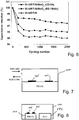
- Fig. 7 and Fig. 8 schematically illustrate two methods of performing the MnO 2 deposition step.
- hydrazine gas is flowed into a reaction chamber 100 through a hydrazine inlet, and back out from the reaction chamber through a hydrazine outlet.
- Two wafers 105 are shown, on top of a KMnO 4 solution, as discussed above.
- a first beaker 112 of hydrazine is instead placed inside a sealed reaction chamber together with a second beaker 110 with the solution of KMnO 4 , with the wafers 105.
- MnO 2 layer Other methods of applying the MnO 2 layer are also feasible.
- the electroless chemical deposition method is preferred, as it produces the most conformal layer on the silicon-TiN-nanorod scaffold.
- the one-dimensional silicon nanostructures may be laid out in a predetermined pattern, such as nanorod arrays.
- a compactness of up to the range of 1.0-2.0 ⁇ 10 6 nanorods/mm 2 can be suitable for the electroless chemical deposition method.
- electrochemical deposition process a compactness up to the range of 0.5-1.0 ⁇ 10 6 nanorods/mm 2 can be appropriate.
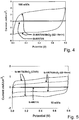
- Fig. 4 depicts two current-voltage-curves for two different supercapacitors with silicon nanorods coated with a TiN layer, measured at 100 mV/s.
- One curve represents an embodiment having only the TiN layer (as known from prior art).
- the other curve is for an embodiment according to the invention, wherein a MnO 2 layer is applied onto the TiN layer.
- the two substantially flat lines close to the zero current value represent the current-voltage diagram for the embodiment without the MnO 2 layer.
- the two other lines represent the current-voltage diagram for the embodiment according to the invention, having the MnO 2 layer.
- This capacitor was produced by applying the MnO 2 layer by means of 16 minutes of electrochemical deposition.
- the calculated capacitance for the embodiment having this Si-TiN-MnO 2 scaffold electrode is 28,4 mF/cm 2 , as evaluated at 100 mV/s scan rate. This is about 30 times higher than that of the Si-TiN electrode.
- Fig. 5 also shows current-voltage curves, corresponding to the diagram discussed above.
- the current-voltage curve of three different capacitors is plotted.
- the curve encapsulating the smallest area represents a capacitor having silicon nanorods coated with SiN, but without any further layer (prior art).
- the two lines (“ED-16min") closest to this curve represent a capacitor with an electrode made of Si nanorods coated with TiN and a MnO 2 layer deposited by means of the electrochemical deposition method for 16 minutes.
- CD-8h represent the current-voltage curve for an embodiment where the MnO 2 layer has been coated onto the TiN layer by means of the developed electroless chemical deposition method for 8 hours.
- the areal capacitance (78,1 mF/cm 2 at 10 mV/s) for the CD-8h embodiment is about 2 times as large as the areal capacitance for the ED-16min embodiment (39,3 mF/cm 2 at 10 mV/s), and about 70 times larger than that of the prior art embodiment lacking the MnO 2 layer (1,15 mF/cm 2 at 10 mV/s).
- Fig. 6 depicts capacitance retention for three different on-chip supercapacitors, after 2000 charge and discharge cycles.
- the upper is a supercapacitor with silicon nanorods provided with TiN and MnO 2 , wherein the MnO 2 layer is loaded with an 8 hours exposure to electroless chemical deposition ("CD-8h” curve).
- the middle curve represents similar nanorods, however having the MnO 2 layer deposited onto the TiN layer by means of 16 minutes electrochemical deposition process (“ED-16min” curve).
- the lower curve represents the capacitance retention of a supercapacitor having the silicon nanorods with only the TiN layer (i.e. no MnO 2 layer), for comparison. It should be noted that although the curves for all three embodiments starts at the 100 % level, they do not exhibit the same capacitance. I.e. the diagram merely illustrate the capacitance retention rate.
- the retention rate of the "CD-8h” curve is significantly less than the "ED-16min” curve, even if both represents supercapacitors having the MnO 2 layer on the TiN layer. While all three curves drop rapidly during the approximately 200 first cycles, the "CD-8h” curve flattens out at about 98 % of the initial capacitance value. The "ED-16min” curve flattens out at about 96-97 %.
- the main reason for capacitance fading is the gradual oxidation of TiN in aqueous electrolyte.
- This problem can be alleviated by conformal coating of MnO 2 on the TiN layer, as a protecting layer. Since the embodiment represented by the "CD-8h” curve (8 hours chemical deposition of MnO 2 ) provides a more conformal and uniform MnO 2 layer than the embodiment represented by the "ED-16min” curve (16 minutes electrochemical deposition of MnO 2 ), better capacitance stability is provided.
- the MnO 2 layer deposited by means of the developed electroless chemical deposition both increases capacitance and increases capacitance retention. Also, due to the conformal deposition of this layer, one may use a silicon-TiN scaffold with relatively densely packed nanorods, without the MnO 2 layer resulting in contact between adjacent nanorods.
- the silicon nanorod TiN scaffold exhibits large mechanical stability. Thus, it assists the outer layer of MnO 2 to tolerate the volume variation that occurs during the redox reaction with solvated sodium ions. This synergetic effect results in an improved cycling performance of the electrode according to the invention.
Landscapes
- Engineering & Computer Science (AREA)
- Power Engineering (AREA)
- Microelectronics & Electronic Packaging (AREA)
- Chemical & Material Sciences (AREA)
- Materials Engineering (AREA)
- Manufacturing & Machinery (AREA)
- Crystallography & Structural Chemistry (AREA)
- Nanotechnology (AREA)
- Chemical Kinetics & Catalysis (AREA)
- Electric Double-Layer Capacitors Or The Like (AREA)
- Semiconductor Memories (AREA)
- Semiconductor Integrated Circuits (AREA)
Description
- The present invention relates to so-called supercapacitors comprising electrodes with a nanostructure scaffold. Such supercapacitors have been shown to exhibit impressive properties that may be exploited in various applications. In particular, the present invention relates to an on-chip supercapacitor that is produced with a method, which is compatible with the fabrication methods for on-chip electric circuitry.
- A group of supercapacitors are called pseudocapacitors. Supercapacitors are high-capacity capacitors with capacitance values much higher than other capacitors. Pseudocapacitors are supercapacitors consisting of both electrical double layer (EDCL) capacitance effect and pseudocapacitance effect, the latter using an electrochemical active material giving an electron charge-transfer between electrolyte and electrode coming from a de-solvated and adsorbed ion. (Reference: Conway, Brian Evans (1999), Electrochemical Supercapacitors: Scientific Fundamentals and Technological Applications (in German), Berlin, Germany: Springer, pp. 1-8, ISBN 0306457369).
- Capacitive units referred to as supercapacitors have been developed, which exploit nanostructure electrodes to obtain high energy densities. However, since overloading (excessive deposition of materials) of the pseudo-capacitive materials that are applied on the electrodes usually causes weak electric conductivity and sluggish ionic conductivity, the obtained capacitance of pseudo-capacitive electrodes is still far below the theoretical values. Thus, an object of the present invention may be to provide a supercapacitor with a nanostructure electrode, which offers improved capacitance and energy density. Another object of the present invention may be to provide a method of producing such a supercapacitor.
- In particular, an object of the present invention may be to provide a conformal coating on the nanostructures, for improved capacitor characteristics.
- Supercapacitors are often referred to as electrochemical capacitors and include both electrical double layer capacitors (EDLC) and pseudocapacitor, the latter also having an electrochemical active material. Supercapacitors are different from conventional dielectric and electrolytic capacitors.
- The article «Fiber Supercapacitors Made of Nanowire-Fiber Hybrid Structures for Wearable/Flexible Energy Storage», J. Bae, Angewandte Chemie. Int. Ed. 50 (2011) 1683-1687, discloses a solution where an array of ZnO nanowires was coated with MnO2 for use in a supercapacitor.
- Silicon as such is not electrochemically stable in commercially available electrolytes. Thus, to employ silicon nanostructures for supercapacitor application, the silicon must be protected by a passivation layer. To fabricate an effective passivation layer on one-dimensional silicon nanostructures has been shown to be difficult. Consequently, there are few references in the prior art describing the use of silicon one-dimensional nanostructures in supercapacitors.
- The article "Nano fabricated silicon nanorod array with titanium nitride coating for on-chip supercapacitors", Lu, Electrochemistry Communications 70 (2016), 51-55, discuss silicon nanorod arrays coated with TiN for use in a supercapacitor.
- Publication
US20140301020 discuss a mesoporous nanocrystalline film architecture for capacitive storage devices. - The present invention provides for an on-chip supercapacitor according to
claim 1 and for a method of providing an on-chip supercapacitor electrode in a silicon substrate according toclaim 7. Embodiments of the invention are set forth with the appended claims. - The present invention is based on providing a layer of manganese dioxide on an elongated / one-dimensional silicon nanostructure that has a layer of titanium nitride (TiN). As used with a supercapacitor according to the invention, the layer of titanium nitride functions as a current collector, while the manganese dioxide layer functions as an electrochemical active material, creating a pseudocapacitor structure.
- In supercapacitors according to the present invention, the TiN layer, which is coated on the Si nanostructure, fulfills two technical objects. One is as a protective passivation layer to avoid the corrosion of electrolyte, and the other is as a current collector.
- According to the invention, there is provided a ternary composite electrode structure based on silicon elongated / one-dimensional nanostructures coated with the titanium nitride nano-layer current collector and manganese dioxide (MnO2) capacitive functional nano-layer. The silicon nanostructure electrode scaffold endow an improved surface gain for energy storage, which is better than that of a flat silicon substrate. The nano-layer of titanium nitride current collector ensures low series resistance and both chemical and mechanical stability of silicon. The conformal and uniform coating of manganese dioxide results in high utilization of active material and a large surface area of active redox centres.
- The possible packing or density of the one-dimensional silicon nanostructures (their mutual distance) will depend on the thickness of the first and second layers. On one hand, it is desirable to obtain a high density of the silicon nanostructures, while on the other hand, the density should preferably not be so high that the deposited layers will abut against layers of neighboring nanostructures.
- Of the same reason, it is preferred that the nanorods are arranged in a structured manner, so that they, with their layers, do not abut against each other. However, an arbitrary arrangement of elongated / one-dimensional nanostructures, be it nanowires or nanorods or other elongated structures, will also be usable for producing a supercapacitor according to the present invention.
- To prevent mutual contact between neighboring elongated nanostructures, it is further preferred that the two layers are conformal. In that way, one prevents that some excessively thick portions of layers result in contact with neighboring structures.
- According to a first aspect of the present invention, there is provided an on-chip supercapacitor according to
claim 1 having an electrode comprising one-dimensional silicon (Si) nanostructures that are coated with a first layer of titanium nitride (TiN). According to the invention, it further comprises a second layer of manganese dioxide (MnO2) deposited on the first layer. - With the term "on-chip", as in "on-chip supercapacitors", it is herein meant capacitors that are produced on silicon chips, produced from silicon wafers, either as independent units or as capacitors in Si-based integrated circuits. In the latter case, the capacitors can typically constitute a functional part of the integrated circuit.
- With the term one-dimensional silicon nanostructure, is herein meant a nanostructure of silicon having an elongated, thin shape, such as a hair (by means of shape, not by means of dimension), with an aspect ratio above 5. Such silicon structures are often referred to in the art as silicon nanorods or nanowires.
- In some embodiments, the one-dimensional silicon nanostructures can extend upright from a silicon base in a pre-determined pattern. That is, the nanostructures, often referred to as nanorods when arranged according to this embodiment, can be produced in predetermined positions on the silicon substrate. This may be done by a top-down or bottom-up method. Typically, the pattern will exhibit a systematic layout of the nanostructures, such as parallel rows. Such rows are often referred to as nanorod arrays. Moreover, the predetermined pattern is such that the nanorods are arranged with a mutual distance between them, so that they are substantially not in contact with each other. Such a distance is appropriate for increasing the capacitance of the supercapacitor. Such a mutual distance should advantageously allow for coating of the current collector layer (TiN), and active material layer (MnO2), and thus provide a large capacitance of the supercapacitor.
- In preferred embodiments, the second layer can be a substantially conformal layer.
- As used herein, the term "conformal layer" shall mean that the outer surface of the conformal layer is substantially parallel with the inner surface of the same layer. Moreover, conformal layer means in the context of the present invention that the coated layer can maintain the morphology of the original template, and the thickness of the coated layer is substantially or nearly identical around the silicon nanostructure.
- Advantageously, according to some embodiments, the second layer has been coated onto the first layer with an electro-less chemical deposition process. Such embodiments will be discussed in detail with reference to example embodiments further below.
- In particular embodiments, the said electroless chemical deposition process may include exposing the nanostructures with the first layer to a solution of KMnO4 that is exposed to an atmosphere containing N2H4 vapor. Advantageously, the solution may be an aqueous solution.
- The concentration of N2H4 vapor can in some embodiments be within the range of 1-10 vol%. In such embodiments and in other embodiments, the gas pressure can be within the range of 1-3 atmospheres.
- Typically, in some embodiments, the N2H4 vapor can be mixed with an inert gas, such as argon (Ar).
- According to a second aspect of the present invention, there is provided a method of providing an on-chip supercapacitor electrode on a silicon substrate according to
claim 7. The method comprises the following steps: - a) providing a plurality of one-dimensional silicon nanostructures on a substrate;
- b) coating the one-dimensional silicon nanostructures with a first layer of titanium nitride (TiN);
- c) coating a second layer of manganese dioxide (MnO2) onto the first layer.
- In some embodiments of the method according to the second aspect of the invention, step c) may comprise an electroless chemical deposition process.
- Advantageously, the second layer is a conformal layer.
- In some embodiments, step c) of the method can include the following step:
- i) in a reaction chamber, exposing the one-dimensional silicon nanostructures (3) to a solution containing KMnO4, wherein the solution is exposed to N2H4 gas.
- The KMnO4-containing solution can advantageously be an aqueous solution.
- Step i) may advantageously include performing step c) for a reaction period of between 6 and 12 hours.
- Supercapacitors are different from the conventional dielectric capacitors from the viewpoint of energy storage mechanism, which stores energy by formation of electric double layer (thickness in nanometer scale) between electrode and electrolyte interface (electric double layer supercapacitor), or by reversible faradic reaction between active electrode material and electrolyte at their interface (pseudo-capacitor). In the supercapacitor provided according to the present invention, the Si/TiN/MnO2 electrode is used to configure a pseudo-capacitor.
- While a general discussion of the present invention has been given above, some more detailed examples of embodiment are given in the following with reference to the drawings, in which
-
Fig. 1 depicts a principle perspective view of silicon nanorod arrays produced in a silicon wafer; -
Fig. 2 is an enlarged cross section view of one nanorod, having a first and a second layer deposited onto it; -
Fig. 3a to Fig. 3d principally illustrate the production of coated silicon nanostructures used in a supercapacitor according to the present invention; -
Fig. 4 is a current-voltage diagram for a supercapacitor according to prior art and a supercapacitor according to the invention; -
Fig. 5 is a current-voltage diagram for a supercapacitor according to prior art and for two supercapacitors according to the invention; -
Fig. 6 depicts capacitance retention for three different on-chip supercapacitors, of which one is according to prior art and the other two are according to the present invention; -
Fig. 7 schematically illustrates a setup for performing the MnO2 deposition step; and -
Fig. 8 schematically illustrates an alternative setup for performing the MnO2 deposition step. -
Fig. 1 illustratessilicon nanorod arrays 1 comprisingsilicon nanorods 3 extending upwards from asilicon base 5. Thenanorods 3 can typically be produced with deep reactive ion etching (DRIE) in a silicon wafer. Typical heights of thenanorods 3 can be between 3 and 6 µm. In some embodiments, typical height is 5 µm. Typical widths or diameters of the nanorod trunks can be between 0,2 to 1,5 µm, more typically about 0,5 µm. -
Fig. 2 depicts a cross section through one of thenanorods 3. Thesilicon nanorod 3 has been coated with afirst layer 10 and asecond layer 20. According to the invention, thefirst layer 10 is a titanium nitride (TiN) layer. Also according to the present invention, thesecond layer 20 is a manganese dioxide (MnO2) layer. - As the skilled person will appreciate, the illustrations of
Fig. 1 and Fig. 2 are principle drawings only, in which layer thickness, aspect ratios, shape etc. not necessarily are correct. - The
first layer 10 of TiN can advantageously be between 10 and 50 nm thick, preferably between 20 and 40 nm, and more preferably about 30 nm thick. Thesecond layer 20 of MnO2 can advantageously be between 50 and 150 nm thick, preferably between 70 and 120 nm, and more preferably between 80 and 100 nm thick. - While some dimensions of the nanorods and the first and second layers are suggested herein, embodiments having other dimensions may also fall within the scope of the present invention.
-
Fig. 3a to Fig. 3d principally depicts the steps of producing a silicon nanorod array coated with the first and second layer, according to an embodiment of the present invention. All four figures are cross section side views through an upper part of asilicon wafer 7. -
Fig. 3a principally depicts a part of asilicon wafer 7, which has not yet been processed. With a DRIE process (deep reactive ion etching), silicon material is removed from the wafer, leaving a plurality ofsilicon nanorods 3 extending in an upright orientation, from thesilicon base 5, as shown inFig. 3b . As the skilled person will appreciate, the shape of thenanorods 3 in a more realistic embodiment may have a larger aspect ratio (length/diameter) than what is shown inFig. 3b . Also, their shape may be less coned, i.e. more symmetrical. -
Fig. 3c depicts thenanorods 3 after having been coated with thefirst layer 10, comprising TiN. Finally,Fig. 3d depicts thenanorods 3 having been coated also with the second layer, comprising MnO2. - To produce the nanorods in a silicon wafer, a cyclic DRIE (deep reactive ion etching) process can be used. Such a process is known to the person skilled in the art, and will not be discussed in detail herein. While the DRIE process is a so-called top-down process, where silicon material is removed to obtain remaining nanorods, one may also employ a bottom-up process to produce the elongated nanostructures.
- After producing the silicon nanorods, they are coated with a layer of TiN. This can advantageously be performed with an atomic layer deposition (ALD) process. This is also a process known to the skilled person. Details of these processes, for the production of the nanorods used with an embodiment of the present invention can be found in the following two papers:
- Lu (P. Lu, P. Ohlckers, L. Mueller, S. Leopold, M. Hoffmann, K. Grigoras, J. Ahopelto, M. Prunnila, X. Y. Chen), "Nano fabricated silicon nanorod array with titanium nitride coating for on-chip supercapacitors" Electrochem. Commun. 70 (2016) 51-55; and
- Mueller (L. Mueller, I. Kapplinger, S. Biermann, W. Brode, M. Hoffmann, J.), «Infrared emitting nanostructures for highly efficient microhotplates», Micromech. Microeng. 24 (2014) 035014.
- In order to obtain a high areal capacitance, one wants to obtain sufficient mass loading of MnO2 anchored to the trunks of the nanorods.
- In one embodiment, the MnO2 layer can be produced with an electrochemical deposition (ED) method. Advantageously, a layer of MnO2 can be deposited on the Si-NR/TiN (silicon nanorod titanium nitride) scaffold by a galvanostatic process at a current density of 0.1 - 0.8, preferably 0.4 mA/cm2 for 10-40, preferably 12-20 minutes, conducted in an aqueous solution of 0.005-0.02, preferably 0.01 M Mn(CH3COO)2 and 0.01-0.04, preferably 0.02 M Na2SO4, performed in a three-electrode system (Ag/AgCI (in saturated KCI) reference electrode and Pt foil counter electrode) at room temperature.
- While the use of the electrochemical deposition method to coat the nanorods produces supercapacitors having good properties, the anticipated surface gain endowed by the Si-TiN nanorods scaffold has not been fully attained. Results have shown that MnO2 tends to clog at the top portions of the nanorods. It is expected that this is a result of the inhomogeneous electric field distribution during the electrochemical deposition.
- In an alternative embodiment, the MnO2 layer can be produced with an electroless chemical deposition (CD) of MnO2 Such deposition can in some embodiments be performed at room temperature by a modified method disclosed in " Nanoporous metal/oxide hybrid electrodes for electrochemical supercapacitors", Chen et al., .
- Specifically, Si-NR/TiN (silicon nanorods with titanium nitride layer) samples can be floated on or submerged in an aqueous solution (e.g. 200 mL) containing 1 to 4 mM, preferably 2 mM KMnO4 and 2 to 10 mM, preferably 5 mM KOH in a first beaker (e.g. a 200 mL beaker).
- Hydrazine, for instance 400 mL 40-50 wt% hydrazine, can be loaded in a second beaker (e.g. a 500 mL beaker). The first and second beakers can be placed in a sealed chamber. During the reaction process, preferably between 6 and 12 hours, the volatile N2H4 as the reductant is introduced to the KMnO4 solution, thus giving rise to MnO2 grown onto the Si-NR/TiN scaffold.
- Instead of performing the above process in room temperature, one may also use temperatures outside room temperatures. For instance, one may use a temperature within the range of 20 to 80 °C.
- One may advantageously perform the above deposition process at ambient pressure, i.e. at 1 atmosphere. One may in some embodiments perform the process within a pressure range of 1 to 3 atm. A process pressure different from ambient pressure will require a pressure vessel.
- The process time may be within the range of 1 to 12 hours.
- An elevated pressure and/or elevated temperature will reduce the needed process time. This may be advantageous in particular in a chip production line at a fabric.
- When floating the wafers on the KMnO4 solution, the face of the wafer where the TiN coated nanorods are provided faces down into the solution. I.e. the scaffold is wetted with the KMnO4 solution. One may also submerge the entire wafer into the solution, but then the opposite side of the wafer would be contaminated by the KMnO4 solution, which normally may not be preferred.
- During this deposition process, where MnO2 is grown or deposited onto the Si-TiN scaffold, the N2H4 vapor diffuses into the liquid KMnO4 solution, and the MnO2 will be formed by the reaction between KMnO4 and N2H4 on TiN layer.
- During this deposition process, the following reaction takes place, resulting in the conformal MnO2 layer on the TiN layer:
4KMnO4 + 3N2H4 → 4MnO2 + 3N2 + 4H2O + 4KOH
- The electroless chemical deposition results in far better MnO2 layer conformity, as compared to the electrochemical deposition process discussed above. Characterization by use of energy-dispersive X-ray spectroscopy (EDX) has shown that in one embodiment, the atomic percentage of Mn in the nanorod tip is close to that in the nanorod trunk (13,2 % vs. 12,4 %, respectively). Thus, by using the CD layer deposition process, a conformal layer of MnO2 is provided to the TiN coated silicon nanorod scaffold.
- This deposition method, for obtaining a conformal layer of MnO2 on the silicon TiN nanostructure scaffold is suitable for implementation in a silicon integrated circuit production line. The process can then be performed as three-step batch process:
- (1) Silicon wafers can be etched by DRIE on a silicon etching production line;
- (2) ALD (atomic layer deposition) TiN growth can be performed on an ALD production line;
- (3) MnO2 growth can be provided by holding the fabricated Si wafer, with the Si-TiN scaffold down on a KMnO4 solution (in a suitably sized container, the size depending on the production scale), in a MnO2 deposition production line.
- The hydrazine atmosphere in step (3) can be provided by steaming the liquid hydrazine. Both sealed or opened reaction container can be used. The critical point is to keep the hydrazine concentration sufficiently constant by continuous feeding of new hydrazine steam.
-
Fig. 7 and Fig. 8 schematically illustrate two methods of performing the MnO2 deposition step. InFig. 7 , hydrazine gas is flowed into areaction chamber 100 through a hydrazine inlet, and back out from the reaction chamber through a hydrazine outlet. Twowafers 105 are shown, on top of a KMnO4 solution, as discussed above. InFig. 8 , afirst beaker 112 of hydrazine is instead placed inside a sealed reaction chamber together with asecond beaker 110 with the solution of KMnO4, with thewafers 105. - Other methods of applying the MnO2 layer are also feasible. One may for instance use electrochemical plating. However, the electroless chemical deposition method is preferred, as it produces the most conformal layer on the silicon-TiN-nanorod scaffold.
- Due to the different results from the different methods of depositing the MnO2 layer (electrochemical deposition and electroless chemical deposition discussed above), different compactness of the silicon nanostructures may be employed. As discussed above, the one-dimensional silicon nanostructures may be laid out in a predetermined pattern, such as nanorod arrays. In such nanorod array embodiments, a compactness of up to the range of 1.0-2.0 × 10⁶ nanorods/mm2 can be suitable for the electroless chemical deposition method. With the electrochemical deposition process, a compactness up to the range of 0.5-1.0 × 10⁶ nanorods/mm2 can be appropriate.
-
Fig. 4 depicts two current-voltage-curves for two different supercapacitors with silicon nanorods coated with a TiN layer, measured at 100 mV/s. One curve represents an embodiment having only the TiN layer (as known from prior art). The other curve is for an embodiment according to the invention, wherein a MnO2 layer is applied onto the TiN layer. In this diagram, the two substantially flat lines close to the zero current value, represent the current-voltage diagram for the embodiment without the MnO2 layer. The two other lines represent the current-voltage diagram for the embodiment according to the invention, having the MnO2 layer. This capacitor was produced by applying the MnO2 layer by means of 16 minutes of electrochemical deposition. This figure clearly demonstrates how the MnO2 layer significantly contributes to the areal capacitance (compare the significantly larger area enclosed by the Si-TiN-MnO2 scaffold with the Si-TiN scaffold). The calculated capacitance for the embodiment having this Si-TiN-MnO2 scaffold electrode is 28,4 mF/cm2, as evaluated at 100 mV/s scan rate. This is about 30 times higher than that of the Si-TiN electrode. -
Fig. 5 also shows current-voltage curves, corresponding to the diagram discussed above. In this diagram, the current-voltage curve of three different capacitors is plotted. Referring toFig. 5 , the curve encapsulating the smallest area (appearing almost as two parallel lines or one line at the zero current level), represents a capacitor having silicon nanorods coated with SiN, but without any further layer (prior art). The two lines ("ED-16min") closest to this curve represent a capacitor with an electrode made of Si nanorods coated with TiN and a MnO2 layer deposited by means of the electrochemical deposition method for 16 minutes. Finally, the uppermost and lowermost lines ("CD-8h") represent the current-voltage curve for an embodiment where the MnO2 layer has been coated onto the TiN layer by means of the developed electroless chemical deposition method for 8 hours. As can be seen in this figure, the areal capacitance (78,1 mF/cm2 at 10 mV/s) for the CD-8h embodiment is about 2 times as large as the areal capacitance for the ED-16min embodiment (39,3 mF/cm2 at 10 mV/s), and about 70 times larger than that of the prior art embodiment lacking the MnO2 layer (1,15 mF/cm2 at 10 mV/s). -
Fig. 6 depicts capacitance retention for three different on-chip supercapacitors, after 2000 charge and discharge cycles. Of the three curves, the upper is a supercapacitor with silicon nanorods provided with TiN and MnO2, wherein the MnO2 layer is loaded with an 8 hours exposure to electroless chemical deposition ("CD-8h" curve). The middle curve represents similar nanorods, however having the MnO2 layer deposited onto the TiN layer by means of 16 minutes electrochemical deposition process ("ED-16min" curve). The lower curve represents the capacitance retention of a supercapacitor having the silicon nanorods with only the TiN layer (i.e. no MnO2 layer), for comparison. It should be noted that although the curves for all three embodiments starts at the 100 % level, they do not exhibit the same capacitance. I.e. the diagram merely illustrate the capacitance retention rate. - It is clear that the retention rate of the "CD-8h" curve is significantly less than the "ED-16min" curve, even if both represents supercapacitors having the MnO2 layer on the TiN layer. While all three curves drop rapidly during the approximately 200 first cycles, the "CD-8h" curve flattens out at about 98 % of the initial capacitance value. The "ED-16min" curve flattens out at about 96-97 %.
- With regard to the lower curve, representing the TiN layered silicon nanorod arrays without any further layer, the main reason for capacitance fading is the gradual oxidation of TiN in aqueous electrolyte. This problem can be alleviated by conformal coating of MnO2 on the TiN layer, as a protecting layer. Since the embodiment represented by the "CD-8h" curve (8 hours chemical deposition of MnO2) provides a more conformal and uniform MnO2 layer than the embodiment represented by the "ED-16min" curve (16 minutes electrochemical deposition of MnO2), better capacitance stability is provided.
- Thus, the MnO2 layer deposited by means of the developed electroless chemical deposition, as discussed above, both increases capacitance and increases capacitance retention. Also, due to the conformal deposition of this layer, one may use a silicon-TiN scaffold with relatively densely packed nanorods, without the MnO2 layer resulting in contact between adjacent nanorods.
- The silicon nanorod TiN scaffold exhibits large mechanical stability. Thus, it assists the outer layer of MnO2 to tolerate the volume variation that occurs during the redox reaction with solvated sodium ions. This synergetic effect results in an improved cycling performance of the electrode according to the invention.
Claims (11)
- An on-chip supercapacitor having an electrode comprising one-dimensional silicon (Si) nanostructures (3) coated with a first layer (10) of titanium nitride (TiN), characterized in that it further comprises a second layer (20) of manganese dioxide (MnO2) deposited on the first layer.
- An on-chip supercapacitor according to claim 1, characterized in that the one-dimensional silicon nanostructures (3) extend upright from a silicon base (5) in a pre-determined pattern.
- An on-chip supercapacitor according to claim 1 or claim 2, characterized in that the second layer (20) is a substantially conformal layer.
- An on-chip supercapacitor according to claim 1, 2 or 3, characterized in that the second layer (20) has been coated onto the first layer (10) with an electroless chemical deposition process.
- An on-chip supercapacitor according to claim 4, characterized in that the said electroless chemical deposition process includes exposing the nanostructures (3) with the first layer (10) to a solution of KMnO4 that is exposed to an atmosphere containing N2H4 vapor.
- An on-chip supercapacitor according to claim 5, characterized in that the concentration of N2H4 vapor is within the range of 1-10 vol% and that the gas pressure is within the range of 1-3 atmospheres.
- A method of providing an on-chip supercapacitor electrode on a silicon substrate, comprising the following steps:a) providing a plurality of one-dimensional silicon nanostructures (3) on a substrate (5);b) coating the one-dimensional silicon nanostructures (3) with a first layer (10) of titanium nitride (TiN);
characterized in that the method further comprises the following step:c) coating a second layer (20) of manganese dioxide (MnO2) onto the first layer (10). - A method according to claim 7, characterized in that step c) comprises an electroless chemical deposition process.
- A method according to claim 7 or claim 8, characterized in that the second layer (20) is a conformal layer.
- A method according to claim 8 or claim 9, characterized in that step c) includes the following step:i) in a reaction chamber, exposing the one-dimensional silicon nanostructures (3) to a solution containing KMnO4, wherein the solution is exposed to N2H4 gas.
- A method according to claim 10, characterized in that step i) includes performing step c) for a reaction period of between 6 and 12 hours.
Applications Claiming Priority (2)
| Application Number | Priority Date | Filing Date | Title |
|---|---|---|---|
| NO20170334A NO343382B1 (en) | 2017-03-07 | 2017-03-07 | On-chip supercapacitor With Silicon nanostructure |
| PCT/EP2018/055471 WO2018162479A1 (en) | 2017-03-07 | 2018-03-06 | On-chip supercapacitor with silicon nanostructure |
Publications (2)
| Publication Number | Publication Date |
|---|---|
| EP3593370A1 EP3593370A1 (en) | 2020-01-15 |
| EP3593370B1 true EP3593370B1 (en) | 2021-05-19 |
Family
ID=61599147
Family Applications (1)
| Application Number | Title | Priority Date | Filing Date |
|---|---|---|---|
| EP18709548.4A Active EP3593370B1 (en) | 2017-03-07 | 2018-03-06 | On-chip supercapacitor with silicon nanostructure |
Country Status (5)
| Country | Link |
|---|---|
| US (1) | US11101082B2 (en) |
| EP (1) | EP3593370B1 (en) |
| CN (1) | CN110462773B (en) |
| NO (1) | NO343382B1 (en) |
| WO (1) | WO2018162479A1 (en) |
Families Citing this family (7)
| Publication number | Priority date | Publication date | Assignee | Title |
|---|---|---|---|---|
| EP3593371B1 (en) | 2017-03-07 | 2021-05-19 | University of South-Eastern Norway | Deposited carbon film on etched silicon for on-chip supercapacitor |
| CN110092346B (en) * | 2019-04-17 | 2022-06-07 | 西安交通大学 | Silicon-based MEMS super capacitor and preparation method thereof |
| FI129648B (en) | 2019-12-20 | 2022-06-15 | Aalto Univ Foundation Sr | Electrode structure |
| CN112331492A (en) * | 2020-11-02 | 2021-02-05 | 马鞍山安慧智电子科技有限公司 | Preparation method of self-supporting porous silicon/ZnO composite material |
| CN116941027A (en) | 2021-02-08 | 2023-10-24 | 麦克德米德乐思公司 | Method and wet chemistry for diffusion barrier formation |
| MA64166A1 (en) * | 2022-07-29 | 2024-12-31 | Guangdong Brunp Recycling Technology Co., Ltd. | COATING METHOD FOR LITHIUM-NICKEL-COBALT-MANGANESE OXIDE POSITIVE ELECTRODE MATERIAL |
| CN115275143B (en) * | 2022-07-29 | 2025-05-27 | 广东邦普循环科技有限公司 | A coating method for lithium nickel cobalt manganese oxide positive electrode material |
Family Cites Families (25)
| Publication number | Priority date | Publication date | Assignee | Title |
|---|---|---|---|---|
| JP3800726B2 (en) * | 1997-05-22 | 2006-07-26 | カシオ計算機株式会社 | Electric double layer capacitor |
| KR100537512B1 (en) | 2003-09-01 | 2005-12-19 | 삼성에스디아이 주식회사 | carbon-nano tube structure and manufacturing method thereof and field emitter and display device both adopting the same |
| US20080248192A1 (en) | 2006-09-11 | 2008-10-09 | Long Jeffrey W | Electroless deposition of nanoscale manganese oxide on ultraporous carbon nanoarchitectures |
| WO2010144153A2 (en) * | 2009-01-09 | 2010-12-16 | The Regents Of The University Of California | Mesoporous nanocrystalline film architecture for capacitive storage devices |
| KR20110008398A (en) | 2009-07-20 | 2011-01-27 | 삼성전자주식회사 | Membrane Structure, Capacitors Comprising the Same, and Manufacturing Method Thereof |
| CA2712051A1 (en) | 2010-08-12 | 2012-02-12 | The Governors Of The University Of Alberta | Method of fabricating a carbon nanotube array |
| US8780526B2 (en) | 2010-06-15 | 2014-07-15 | Applied Nanostructured Solutions, Llc | Electrical devices containing carbon nanotube-infused fibers and methods for production thereof |
| CN102468056B (en) * | 2010-11-11 | 2014-11-05 | 中国科学院青岛生物能源与过程研究所 | Electrode material of supercapacitor, and manufacturing method and application of electrode material |
| US20120236467A1 (en) | 2011-03-16 | 2012-09-20 | Vanderbilt University, Center For Technology Transfer And Commercialization | Ultracapacitor, methods of manufacturing and applications of the same |
| US8503161B1 (en) | 2011-03-23 | 2013-08-06 | Hrl Laboratories, Llc | Supercapacitor cells and micro-supercapacitors |
| WO2013037951A1 (en) | 2011-09-16 | 2013-03-21 | Danmarks Tekniske Universitet | Catalyst deposition for the preparation of carbon nanotubes |
| US8663841B2 (en) | 2011-09-16 | 2014-03-04 | Semiconductor Energy Laboratory Co., Ltd. | Power storage device |
| WO2013050570A1 (en) | 2011-10-05 | 2013-04-11 | Lightlab Sweden Ab | Method for manufacturing nanostructures and cathode for field emission lighting arrangement |
| WO2013100916A1 (en) | 2011-12-27 | 2013-07-04 | Intel Corporation | Fabrication of porous silicon electrochemical capacitors |
| CN102737859A (en) | 2012-07-06 | 2012-10-17 | 海博瑞恩电子科技无锡有限公司 | Manufacturing method of three-dimensional MEMS (micro-electromechanical systems) super capacitor based on silicon-based deep etching process |
| SG11201502983SA (en) | 2012-10-17 | 2015-05-28 | Univ Singapore Technology & Design | High specific capacitance and high power density of printed flexible micro-supercapacitors |
| US9053843B2 (en) | 2013-01-22 | 2015-06-09 | Bluestone Technologies (Cayman) Limited | Graphene hybrid structures for energy storage applications |
| US20160107178A1 (en) | 2013-05-28 | 2016-04-21 | Massachusetts Institute Of Technology | Electrospraying systems and associated methods |
| US9728344B2 (en) | 2013-09-04 | 2017-08-08 | Oregon State University | Energy storage device including a redox-enhanced electrolyte |
| US10319535B2 (en) | 2013-09-27 | 2019-06-11 | Intel Corporation | High voltage high power energy storage devices, systems, and associated methods |
| US9640332B2 (en) * | 2013-12-20 | 2017-05-02 | Intel Corporation | Hybrid electrochemical capacitor |
| WO2016059296A1 (en) | 2014-10-17 | 2016-04-21 | Teknologian Tutkimuskeskus Vtt Oy | A blank suitable for use as a body of supercapacitor, a supercapacitor, and a method of manufacturing a porous silicon volume |
| MX2017006315A (en) | 2014-11-18 | 2017-08-21 | Univ California | Porous interconnected corrugated carbon-based network (iccn) composite. |
| EP3067313A1 (en) | 2015-03-09 | 2016-09-14 | Consejo Superior De Investigaciones Cientificas | Electrode material comprising silicon nanowires covered by mesoporous oxide nanostructured coating and ionic liguid electrolytes for energy storage applications |
| EP3593371B1 (en) | 2017-03-07 | 2021-05-19 | University of South-Eastern Norway | Deposited carbon film on etched silicon for on-chip supercapacitor |
-
2017
- 2017-03-07 NO NO20170334A patent/NO343382B1/en unknown
-
2018
- 2018-03-06 CN CN201880016550.9A patent/CN110462773B/en active Active
- 2018-03-06 US US16/491,298 patent/US11101082B2/en active Active
- 2018-03-06 WO PCT/EP2018/055471 patent/WO2018162479A1/en not_active Ceased
- 2018-03-06 EP EP18709548.4A patent/EP3593370B1/en active Active
Also Published As
| Publication number | Publication date |
|---|---|
| EP3593370A1 (en) | 2020-01-15 |
| US20200035420A1 (en) | 2020-01-30 |
| NO20170334A1 (en) | 2018-09-10 |
| CN110462773A (en) | 2019-11-15 |
| NO343382B1 (en) | 2019-02-18 |
| US11101082B2 (en) | 2021-08-24 |
| CN110462773B (en) | 2022-04-15 |
| WO2018162479A1 (en) | 2018-09-13 |
Similar Documents
| Publication | Publication Date | Title |
|---|---|---|
| US11101082B2 (en) | On-chip supercapacitor with silicon nanostructure | |
| Raj et al. | Two-dimensional planar supercapacitor based on zinc oxide/manganese oxide core/shell nano-architecture | |
| JP7177822B2 (en) | Conversion of a valve metal layer into a template with a plurality of (nano)channels with defined spacing and formation of structures therein with defined spacing | |
| Wang et al. | Fabrication of a symmetric micro supercapacitor based on tubular ruthenium oxide on silicon 3D microstructures | |
| Wang et al. | A high-performance three-dimensional micro supercapacitor based on ripple-like ruthenium oxide–carbon nanotube composite films | |
| EP3593371B1 (en) | Deposited carbon film on etched silicon for on-chip supercapacitor | |
| Gaboriau et al. | Silicon nanowires and nanotrees: Elaboration and optimization of new 3D architectures for high performance on-chip supercapacitors | |
| Lamiel et al. | 3D hierarchical mesoporous NiCo 2 S 4@ Ni (OH) 2 core–shell nanosheet arrays for high performance supercapacitors | |
| KR20090088427A (en) | Electrodes for use in double electrolayer electrochemical capacitors with high non-parameter values | |
| Rani et al. | Fabrication of binder-free TiO 2 nanofiber electrodes via electrophoretic deposition for low-power electronic applications | |
| Cao et al. | ZnO/ZnS core-shell nanowires arrays on Ni foam prepared by atomic layer deposition for high performance supercapacitors | |
| US20230053249A1 (en) | Dendritic materials with hierarchical porosity | |
| EP4229664B1 (en) | Direct growth cross-linked carbon nanotubes on microstructured metal substrate for supercapacitor application | |
| KR101087266B1 (en) | Method for producing silicon nanowire / ink oxide core / shell nanocomposite and solar cell comprising the nanocomposite | |
| KR20240135751A (en) | Composite electrode material, method for producing the same and uses of the material | |
| CN102074378A (en) | Preparation method for solid state super capacitor | |
| Liu et al. | Passivation of silicon nanowires with Ni particles and a PEDOT/MnO X composite for high-performance aqueous supercapacitors | |
| KR101439788B1 (en) | Fabrication of three dimensional network of carbon nanotubes oriented metal or metal oxide nano-structures by electrochemical method | |
| Grigoras et al. | Porous silicon for energy storage at microscale: Supercapacitors | |
| Tagsin et al. | Synthesis and supercapacitor characteristics of hydrothermally-deposited MnO2 films and chemically Co-deposited MnO2-polyaniline films on stainless-steel substrates | |
| Debbab et al. | Behavior Study of Annealing Temperature on Microstructure and Wettability of Electrodeposited ZnO Thin Films for Microcapacitor Application | |
| El Abedin | 8.4 Electrochemical Synthesis of Nanowire Electrodes for Lithium Batteries | |
| Lobinsky et al. | Red-ox reactions in aqueous solutions of Co (OAc)^ sub 2^ and K^ sub 2^ S^ sub 2^ O^ sub 8^ and synthesis of CoOOH nanolayers by the SILD method | |
| Watts | Coated Silicon Nanowires as Anodes in Lithium Ion Batteries |
Legal Events
| Date | Code | Title | Description |
|---|---|---|---|
| STAA | Information on the status of an ep patent application or granted ep patent |
Free format text: STATUS: UNKNOWN |
|
| STAA | Information on the status of an ep patent application or granted ep patent |
Free format text: STATUS: THE INTERNATIONAL PUBLICATION HAS BEEN MADE |
|
| PUAI | Public reference made under article 153(3) epc to a published international application that has entered the european phase |
Free format text: ORIGINAL CODE: 0009012 |
|
| STAA | Information on the status of an ep patent application or granted ep patent |
Free format text: STATUS: REQUEST FOR EXAMINATION WAS MADE |
|
| 17P | Request for examination filed |
Effective date: 20190919 |
|
| AK | Designated contracting states |
Kind code of ref document: A1 Designated state(s): AL AT BE BG CH CY CZ DE DK EE ES FI FR GB GR HR HU IE IS IT LI LT LU LV MC MK MT NL NO PL PT RO RS SE SI SK SM TR |
|
| AX | Request for extension of the european patent |
Extension state: BA ME |
|
| DAV | Request for validation of the european patent (deleted) | ||
| DAX | Request for extension of the european patent (deleted) | ||
| GRAP | Despatch of communication of intention to grant a patent |
Free format text: ORIGINAL CODE: EPIDOSNIGR1 |
|
| STAA | Information on the status of an ep patent application or granted ep patent |
Free format text: STATUS: GRANT OF PATENT IS INTENDED |
|
| INTG | Intention to grant announced |
Effective date: 20201215 |
|
| RIN1 | Information on inventor provided before grant (corrected) |
Inventor name: OEHLCKERS, PER ALFRED Inventor name: CHEN, XUYUAN Inventor name: LU, PAI |
|
| GRAS | Grant fee paid |
Free format text: ORIGINAL CODE: EPIDOSNIGR3 |
|
| GRAA | (expected) grant |
Free format text: ORIGINAL CODE: 0009210 |
|
| STAA | Information on the status of an ep patent application or granted ep patent |
Free format text: STATUS: THE PATENT HAS BEEN GRANTED |
|
| AK | Designated contracting states |
Kind code of ref document: B1 Designated state(s): AL AT BE BG CH CY CZ DE DK EE ES FI FR GB GR HR HU IE IS IT LI LT LU LV MC MK MT NL NO PL PT RO RS SE SI SK SM TR |
|
| REG | Reference to a national code |
Ref country code: GB Ref legal event code: FG4D |
|
| REG | Reference to a national code |
Ref country code: CH Ref legal event code: EP |
|
| REG | Reference to a national code |
Ref country code: DE Ref legal event code: R096 Ref document number: 602018017280 Country of ref document: DE |
|
| REG | Reference to a national code |
Ref country code: AT Ref legal event code: REF Ref document number: 1394790 Country of ref document: AT Kind code of ref document: T Effective date: 20210615 |
|
| REG | Reference to a national code |
Ref country code: IE Ref legal event code: FG4D |
|
| REG | Reference to a national code |
Ref country code: LT Ref legal event code: MG9D |
|
| REG | Reference to a national code |
Ref country code: AT Ref legal event code: MK05 Ref document number: 1394790 Country of ref document: AT Kind code of ref document: T Effective date: 20210519 |
|
| REG | Reference to a national code |
Ref country code: NL Ref legal event code: MP Effective date: 20210519 |
|
| PG25 | Lapsed in a contracting state [announced via postgrant information from national office to epo] |
Ref country code: BG Free format text: LAPSE BECAUSE OF FAILURE TO SUBMIT A TRANSLATION OF THE DESCRIPTION OR TO PAY THE FEE WITHIN THE PRESCRIBED TIME-LIMIT Effective date: 20210819 Ref country code: AT Free format text: LAPSE BECAUSE OF FAILURE TO SUBMIT A TRANSLATION OF THE DESCRIPTION OR TO PAY THE FEE WITHIN THE PRESCRIBED TIME-LIMIT Effective date: 20210519 Ref country code: FI Free format text: LAPSE BECAUSE OF FAILURE TO SUBMIT A TRANSLATION OF THE DESCRIPTION OR TO PAY THE FEE WITHIN THE PRESCRIBED TIME-LIMIT Effective date: 20210519 Ref country code: HR Free format text: LAPSE BECAUSE OF FAILURE TO SUBMIT A TRANSLATION OF THE DESCRIPTION OR TO PAY THE FEE WITHIN THE PRESCRIBED TIME-LIMIT Effective date: 20210519 Ref country code: LT Free format text: LAPSE BECAUSE OF FAILURE TO SUBMIT A TRANSLATION OF THE DESCRIPTION OR TO PAY THE FEE WITHIN THE PRESCRIBED TIME-LIMIT Effective date: 20210519 |
|
| PG25 | Lapsed in a contracting state [announced via postgrant information from national office to epo] |
Ref country code: GR Free format text: LAPSE BECAUSE OF FAILURE TO SUBMIT A TRANSLATION OF THE DESCRIPTION OR TO PAY THE FEE WITHIN THE PRESCRIBED TIME-LIMIT Effective date: 20210820 Ref country code: IS Free format text: LAPSE BECAUSE OF FAILURE TO SUBMIT A TRANSLATION OF THE DESCRIPTION OR TO PAY THE FEE WITHIN THE PRESCRIBED TIME-LIMIT Effective date: 20210919 Ref country code: LV Free format text: LAPSE BECAUSE OF FAILURE TO SUBMIT A TRANSLATION OF THE DESCRIPTION OR TO PAY THE FEE WITHIN THE PRESCRIBED TIME-LIMIT Effective date: 20210519 Ref country code: PT Free format text: LAPSE BECAUSE OF FAILURE TO SUBMIT A TRANSLATION OF THE DESCRIPTION OR TO PAY THE FEE WITHIN THE PRESCRIBED TIME-LIMIT Effective date: 20210920 Ref country code: PL Free format text: LAPSE BECAUSE OF FAILURE TO SUBMIT A TRANSLATION OF THE DESCRIPTION OR TO PAY THE FEE WITHIN THE PRESCRIBED TIME-LIMIT Effective date: 20210519 Ref country code: NO Free format text: LAPSE BECAUSE OF FAILURE TO SUBMIT A TRANSLATION OF THE DESCRIPTION OR TO PAY THE FEE WITHIN THE PRESCRIBED TIME-LIMIT Effective date: 20210819 Ref country code: RS Free format text: LAPSE BECAUSE OF FAILURE TO SUBMIT A TRANSLATION OF THE DESCRIPTION OR TO PAY THE FEE WITHIN THE PRESCRIBED TIME-LIMIT Effective date: 20210519 Ref country code: SE Free format text: LAPSE BECAUSE OF FAILURE TO SUBMIT A TRANSLATION OF THE DESCRIPTION OR TO PAY THE FEE WITHIN THE PRESCRIBED TIME-LIMIT Effective date: 20210519 |
|
| PG25 | Lapsed in a contracting state [announced via postgrant information from national office to epo] |
Ref country code: NL Free format text: LAPSE BECAUSE OF FAILURE TO SUBMIT A TRANSLATION OF THE DESCRIPTION OR TO PAY THE FEE WITHIN THE PRESCRIBED TIME-LIMIT Effective date: 20210519 |
|
| PG25 | Lapsed in a contracting state [announced via postgrant information from national office to epo] |
Ref country code: SK Free format text: LAPSE BECAUSE OF FAILURE TO SUBMIT A TRANSLATION OF THE DESCRIPTION OR TO PAY THE FEE WITHIN THE PRESCRIBED TIME-LIMIT Effective date: 20210519 Ref country code: SM Free format text: LAPSE BECAUSE OF FAILURE TO SUBMIT A TRANSLATION OF THE DESCRIPTION OR TO PAY THE FEE WITHIN THE PRESCRIBED TIME-LIMIT Effective date: 20210519 Ref country code: ES Free format text: LAPSE BECAUSE OF FAILURE TO SUBMIT A TRANSLATION OF THE DESCRIPTION OR TO PAY THE FEE WITHIN THE PRESCRIBED TIME-LIMIT Effective date: 20210519 Ref country code: EE Free format text: LAPSE BECAUSE OF FAILURE TO SUBMIT A TRANSLATION OF THE DESCRIPTION OR TO PAY THE FEE WITHIN THE PRESCRIBED TIME-LIMIT Effective date: 20210519 Ref country code: RO Free format text: LAPSE BECAUSE OF FAILURE TO SUBMIT A TRANSLATION OF THE DESCRIPTION OR TO PAY THE FEE WITHIN THE PRESCRIBED TIME-LIMIT Effective date: 20210519 Ref country code: CZ Free format text: LAPSE BECAUSE OF FAILURE TO SUBMIT A TRANSLATION OF THE DESCRIPTION OR TO PAY THE FEE WITHIN THE PRESCRIBED TIME-LIMIT Effective date: 20210519 Ref country code: DK Free format text: LAPSE BECAUSE OF FAILURE TO SUBMIT A TRANSLATION OF THE DESCRIPTION OR TO PAY THE FEE WITHIN THE PRESCRIBED TIME-LIMIT Effective date: 20210519 |
|
| REG | Reference to a national code |
Ref country code: DE Ref legal event code: R097 Ref document number: 602018017280 Country of ref document: DE |
|
| PLBE | No opposition filed within time limit |
Free format text: ORIGINAL CODE: 0009261 |
|
| STAA | Information on the status of an ep patent application or granted ep patent |
Free format text: STATUS: NO OPPOSITION FILED WITHIN TIME LIMIT |
|
| 26N | No opposition filed |
Effective date: 20220222 |
|
| PG25 | Lapsed in a contracting state [announced via postgrant information from national office to epo] |
Ref country code: IS Free format text: LAPSE BECAUSE OF FAILURE TO SUBMIT A TRANSLATION OF THE DESCRIPTION OR TO PAY THE FEE WITHIN THE PRESCRIBED TIME-LIMIT Effective date: 20210919 Ref country code: AL Free format text: LAPSE BECAUSE OF FAILURE TO SUBMIT A TRANSLATION OF THE DESCRIPTION OR TO PAY THE FEE WITHIN THE PRESCRIBED TIME-LIMIT Effective date: 20210519 |
|
| PG25 | Lapsed in a contracting state [announced via postgrant information from national office to epo] |
Ref country code: IT Free format text: LAPSE BECAUSE OF FAILURE TO SUBMIT A TRANSLATION OF THE DESCRIPTION OR TO PAY THE FEE WITHIN THE PRESCRIBED TIME-LIMIT Effective date: 20210519 |
|
| PG25 | Lapsed in a contracting state [announced via postgrant information from national office to epo] |
Ref country code: MC Free format text: LAPSE BECAUSE OF FAILURE TO SUBMIT A TRANSLATION OF THE DESCRIPTION OR TO PAY THE FEE WITHIN THE PRESCRIBED TIME-LIMIT Effective date: 20210519 |
|
| REG | Reference to a national code |
Ref country code: CH Ref legal event code: PL |
|
| REG | Reference to a national code |
Ref country code: BE Ref legal event code: MM Effective date: 20220331 |
|
| PG25 | Lapsed in a contracting state [announced via postgrant information from national office to epo] |
Ref country code: LU Free format text: LAPSE BECAUSE OF NON-PAYMENT OF DUE FEES Effective date: 20220306 Ref country code: LI Free format text: LAPSE BECAUSE OF NON-PAYMENT OF DUE FEES Effective date: 20220331 Ref country code: IE Free format text: LAPSE BECAUSE OF NON-PAYMENT OF DUE FEES Effective date: 20220306 Ref country code: CH Free format text: LAPSE BECAUSE OF NON-PAYMENT OF DUE FEES Effective date: 20220331 |
|
| PG25 | Lapsed in a contracting state [announced via postgrant information from national office to epo] |
Ref country code: BE Free format text: LAPSE BECAUSE OF NON-PAYMENT OF DUE FEES Effective date: 20220331 |
|
| PG25 | Lapsed in a contracting state [announced via postgrant information from national office to epo] |
Ref country code: MK Free format text: LAPSE BECAUSE OF FAILURE TO SUBMIT A TRANSLATION OF THE DESCRIPTION OR TO PAY THE FEE WITHIN THE PRESCRIBED TIME-LIMIT Effective date: 20210519 Ref country code: CY Free format text: LAPSE BECAUSE OF FAILURE TO SUBMIT A TRANSLATION OF THE DESCRIPTION OR TO PAY THE FEE WITHIN THE PRESCRIBED TIME-LIMIT Effective date: 20210519 |
|
| PG25 | Lapsed in a contracting state [announced via postgrant information from national office to epo] |
Ref country code: HU Free format text: LAPSE BECAUSE OF FAILURE TO SUBMIT A TRANSLATION OF THE DESCRIPTION OR TO PAY THE FEE WITHIN THE PRESCRIBED TIME-LIMIT; INVALID AB INITIO Effective date: 20180306 |
|
| PG25 | Lapsed in a contracting state [announced via postgrant information from national office to epo] |
Ref country code: TR Free format text: LAPSE BECAUSE OF FAILURE TO SUBMIT A TRANSLATION OF THE DESCRIPTION OR TO PAY THE FEE WITHIN THE PRESCRIBED TIME-LIMIT Effective date: 20210519 |
|
| PG25 | Lapsed in a contracting state [announced via postgrant information from national office to epo] |
Ref country code: MT Free format text: LAPSE BECAUSE OF FAILURE TO SUBMIT A TRANSLATION OF THE DESCRIPTION OR TO PAY THE FEE WITHIN THE PRESCRIBED TIME-LIMIT Effective date: 20210519 |
|
| PGFP | Annual fee paid to national office [announced via postgrant information from national office to epo] |
Ref country code: GB Payment date: 20260317 Year of fee payment: 9 |
|
| PGFP | Annual fee paid to national office [announced via postgrant information from national office to epo] |
Ref country code: DE Payment date: 20260318 Year of fee payment: 9 |
|
| PGFP | Annual fee paid to national office [announced via postgrant information from national office to epo] |
Ref country code: FR Payment date: 20260317 Year of fee payment: 9 |