EP3591842A1 - Rc oscillator watchdog circuit - Google Patents
Rc oscillator watchdog circuit Download PDFInfo
- Publication number
- EP3591842A1 EP3591842A1 EP19184330.9A EP19184330A EP3591842A1 EP 3591842 A1 EP3591842 A1 EP 3591842A1 EP 19184330 A EP19184330 A EP 19184330A EP 3591842 A1 EP3591842 A1 EP 3591842A1
- Authority
- EP
- European Patent Office
- Prior art keywords
- node
- circuit
- oscillator
- coupled
- cap
- Prior art date
- Legal status (The legal status is an assumption and is not a legal conclusion. Google has not performed a legal analysis and makes no representation as to the accuracy of the status listed.)
- Granted
Links
Images




Classifications
-
- H—ELECTRICITY
- H03—ELECTRONIC CIRCUITRY
- H03K—PULSE TECHNIQUE
- H03K3/00—Circuits for generating electric pulses; Monostable, bistable or multistable circuits
- H03K3/02—Generators characterised by the type of circuit or by the means used for producing pulses
- H03K3/023—Generators characterised by the type of circuit or by the means used for producing pulses by the use of differential amplifiers or comparators, with internal or external positive feedback
- H03K3/0231—Astable circuits
-
- H—ELECTRICITY
- H03—ELECTRONIC CIRCUITRY
- H03K—PULSE TECHNIQUE
- H03K3/00—Circuits for generating electric pulses; Monostable, bistable or multistable circuits
- H03K3/01—Details
- H03K3/011—Modifications of generator to compensate for variations in physical values, e.g. voltage, temperature
-
- H—ELECTRICITY
- H03—ELECTRONIC CIRCUITRY
- H03K—PULSE TECHNIQUE
- H03K4/00—Generating pulses having essentially a finite slope or stepped portions
- H03K4/06—Generating pulses having essentially a finite slope or stepped portions having triangular shape
- H03K4/08—Generating pulses having essentially a finite slope or stepped portions having triangular shape having sawtooth shape
- H03K4/48—Generating pulses having essentially a finite slope or stepped portions having triangular shape having sawtooth shape using as active elements semiconductor devices
- H03K4/50—Generating pulses having essentially a finite slope or stepped portions having triangular shape having sawtooth shape using as active elements semiconductor devices in which a sawtooth voltage is produced across a capacitor
- H03K4/501—Generating pulses having essentially a finite slope or stepped portions having triangular shape having sawtooth shape using as active elements semiconductor devices in which a sawtooth voltage is produced across a capacitor the starting point of the flyback period being determined by the amplitude of the voltage across the capacitor, e.g. by a comparator
- H03K4/502—Generating pulses having essentially a finite slope or stepped portions having triangular shape having sawtooth shape using as active elements semiconductor devices in which a sawtooth voltage is produced across a capacitor the starting point of the flyback period being determined by the amplitude of the voltage across the capacitor, e.g. by a comparator the capacitor being charged from a constant-current source
-
- H—ELECTRICITY
- H03—ELECTRONIC CIRCUITRY
- H03K—PULSE TECHNIQUE
- H03K5/00—Manipulating of pulses not covered by one of the other main groups of this subclass
- H03K5/19—Monitoring patterns of pulse trains
Definitions
- This disclosure is related to the field of RC oscillator circuits, and in particular, to a watchdog circuit for RC oscillators that detects incorrect operation of an RC oscillator circuit so that a reset of the RC oscillator circuit can be triggered.
- SoC system on a chip
- a SoC typically receives its clock signal from a crystal oscillator.
- the startup time of a crystal oscillator is relatively slow, being on the order of miliseconds.
- an RC oscillator is typically used to provide a clock signal for the SoC to use during its startup process, as the startup time of the RC oscillator is relatively quick, on the order of microseconds.
- the RC oscillator 50 includes a SR flip flop 56 having a set input S, a reset input R, a non-inverting output Q, and an inverting output Qbar.
- Comparator 52 provides output to the set input S, while comparator 54 provides output to the reset input R.
- a current generator 51 generates a bias current Ibias.
- Resistor R1 is coupled between the current generator 51 and the non-inverting input of the comparator 52, while resistor R2 is coupled between the current generator 51 and the non-inverting input of the comparator 54.
- a reference voltage Vref is coupled to the inverting inputs of the comparators 52 and 54.
- Capacitor C1 is coupled between the non-inverting input of the comparator 52 and ground, while capacitor C2 is coupled between the non-inverting input of the comparator 54 and ground.
- a switch S1 selectively shunts capacitor C1 to ground in response to assertion of the non-inverting output Q of the SR flip flop 56, while switch S2 selectively shunts capacitor C2 to ground in response to assertion of the inverting output Qbar of the flip flop 56.
- the comparator 52 When the voltage across capacitor C1 rises to be equal to the reference voltage Vref, the comparator 52 will assert its output, causing the SR flip flop 56 to set, asserting Q and deasserting Qbar. This in turn causes switch S1 to close to discharge capacitor C1, and switch S2 to open to charge capacitor C2. When the voltage across capacitor C2 rises to be equal to Vref, the comparator 54 will assert its output, resetting the SR flip flop 56 to the state initially discussed.
- This repeated operation yields a clock signal CK at the non-inverting output Q of the SR flip flop 56 that, provided the values of R1 and R2 are the same and the values of C1 and C2 are the same, is a square wave.
- a first aspect disclosed herein is a circuit that includes a RC oscillator and an oscillator fault detection circuit.
- the RC oscillator includes a first comparison circuit, a second comparison circuit, a logic circuit receiving output from the first and second comparison circuits as input and generating a logic output signal, and a clock generation circuit generating a clock signal as a function of the logic output signal.
- the oscillator fault detection circuit includes a capacitive node, charge circuitry configured to selectively charge the capacitive node based upon the logic output signal, discharge circuitry configured to selectively discharge the capacitive node based upon the logic output signal, and triggering circuitry configured to assert a reset signal when the charge on the capacitive node indicates a fault with the RC oscillator.
- the discharge circuitry fails to discharge the capacitive node to a lower threshold when the logic output signal transitions in a pattern indicating proper operation of the RC oscillator.
- the charge on the capacitive node being above the lower threshold indicates proper operation of the RC oscillator.
- the discharge circuitry begins to discharge the capacitive node to below a lower threshold when the logic output signal fails to transition in a pattern indicating proper operation of the RC oscillator.
- the charge on the capacitive node being below the lower threshold indicates a fault with the RC oscillator.
- the charge circuitry maintains the capacitive node above a lower threshold when the logic output signal transitions in a pattern indicating proper operation of the RC oscillator. Charge on the capacitive node being above an upper threshold indicates proper operation of the RC oscillator.
- the reset signal serves to reset the RC oscillator such that the RC oscillator returns to proper operation.
- the charge circuitry charges the capacitive node to back above the lower threshold when the logic output signal returns to a reset state after the RC oscillator has been reset by the reset signal, thereby resulting in the triggering circuitry deasserting the reset signal.
- the charge circuitry does not charge the capacitive node when the logic output signal fails to transition in a pattern indicating proper operation of the RC oscillator.
- the charge circuitry may include an inverter, and the discharge circuitry may also utilize the inverter.
- the charge circuitry further may include a first latch, and the discharge circuitry may include a second latch.
- the triggering circuitry may include a Schmitt trigger.
- the capacitive node may be coupled to at least one field effect transistor (FET) configured as a capacitor.
- FET field effect transistor
- the first comparison circuit may include a first comparator
- the second comparison circuit may include a second comparator
- the logic circuit may include an OR gate
- the reset signal may serve to reset the RC oscillator such that the RC oscillator returns to proper operation.
- the RC oscillator includes a first comparison circuit, a second comparison circuit, a logic circuit receiving output from the first and second comparison circuits as input and generating a logic output signal, and a clock generation circuit generating a clock signal as a function of the logic output signal.
- the oscillator fault detection circuit includes a capacitive node, an inverter coupled to receive the logic output signal and provide output to the capacitive node, a Schmitt trigger having an input coupled to the capacitive node, and at least one inverter coupled between an output of the Schmitt trigger and an output of the oscillator fault.
- the oscillator fault detection circuit may include a buffer coupled between the logic output signal and the inverter, a first PMOS transistor having a source coupled to a supply node, a drain, and a gate coupled to the logic output signal, and a second PMOS transistor having a source coupled to the drain of the first PMOS transistor, a drain coupled to the capacitive node, and a gate coupled to the output of the Schmitt trigger.
- the oscillator fault detection circuit may also include a first NMOS transistor having a drain coupled to the capacitive node, a source, and a gate coupled to the output of the Schmitt trigger, and a second NMOS transistor having a drain coupled to the source of the first NMOS transistor, a source coupled to ground, and a gate coupled to the logic output signal.
- the oscillator fault detection circuit may also include a first PMOS transistor having a source and drain coupled to a supply node and a gate coupled to the capacitive node, and a second PMOS transistor having a source and drain coupled to ground and a gate coupled to the capacitive node.
- Another aspect disclosed herein is a circuit including an RC oscillator configured to generate a periodic trigger signal, a clock generator configured to generate clock edges in response to the periodic trigger signal, and a stuck at fault detection circuit.
- the stuck at fault detection circuit is configured to detect a stuck at logic state of the periodic trigger signal and in response thereto cause the RC oscillator to reset and cause a change in logic state of the periodic trigger signal.
- the RC oscillator may include a first comparison circuit, a second comparison circuit, a logic circuit receiving output from the first and second comparison circuits as input and generating the periodic trigger signal, and a clock generation circuit generating a clock signal as a function of the periodic trigger signal.
- the stuck at fault detection circuit may include a capacitive node, charge circuitry configured to selectively charge the capacitive node based upon the periodic trigger signal, discharge circuitry configured to selectively discharge the capacitive node based upon the periodic trigger signal, and triggering circuitry configured to assert a reset signal to cause the RC oscillator to reset when the charge on the capacitive node indicates a stuck at logic state of the periodic trigger signal.
- an embodiment of an electronic system 1 including a system on a chip (SoC) 2 is now described.
- the SoC 2 is coupled to a memory 3, input/output (I/O) devices 4, a crystal oscillator 5, and a RC oscillator 6.
- I/O input/output
- crystal oscillator 5 outputs signals from a crystal oscillator 5.
- the SoC 2 requires a clock signal CLK2 to begin its own startup operations.
- the crystal oscillator 5 takes a relatively long time (on the order of milliseconds) to begin producing the clock signal CLK1 after power up of the electronic system 1. Therefore, in various embodiments, immediately after power up of the electronic system 1, the RC oscillator 6 is used to produce a clock signal CLK2 for the SoC 2 because the RC oscillator 6 is able to produce the clock signal CLK2 in a short period of time (on the order of microseconds) after power up.
- the RC oscillator 6 includes a current source Gp generating a bias current Ibias.
- This bias current Ibias is received at the input of current mirror 7.
- the output of current mirror 7 draws current Irif into it, and current Irif is proportional to the bias current Ibias.
- the current mirror 7 includes ( e.g ., NMOS) transistor T1 having its drain acting as the input to the current mirror 7, its source coupled to ground, and its gate coupled to its drain.
- the current mirror 7 includes ( e.g ., NMOS) transistor T2 having its drain acting as the output to the current mirror 7, its source coupled to ground, and its gate coupled to the gate of transistor T1.
- current mirror 8 includes (e.g ., PMOS) transistor T3 having its source coupled to supply node Vdd, its drain acting as the input to the current mirror 8, and its gate coupled to its drain.
- PMOS e.g ., PMOS
- transistor T4 has its source coupled to the supply node Vdd, its drain coupled to node 14 to provide output current I1, and its gate coupled to the gate of transistor T3.
- transistor T5 has its source coupled to the supply node Vdd, its drain coupled to node 15 to provide output current 12, and its gate coupled to the gate of transistor T3.
- Transistor T6 has it source coupled to the supply node Vdd, its drain coupled to node 28 to provide output current 13, and its gate coupled to the gate of transistor T3.
- the drains of transistor T4, T5, and T6 form the outputs of the current mirror 8.
- a multiplexer 13 has inputs coupled to nodes 14, 15, and 28 to receive the currents I1, 12, and I3 respectively.
- the multiplexer 13 has outputs coupled to nodes 16, 17, and 18.
- a resistor R is coupled between node 18 and ground.
- Capacitor C3 is coupled between node 17 and ground, and capacitor C4 is coupled between node 16 and ground.
- the multiplexer 13 is controlled by the control signals Ssw received from a control circuit 21.
- a comparator 80 has an inverting terminal receiving a reference voltage Vref from node 18, a non-inverting terminal receiving voltage V1 from node 17, and an output Sc1 coupled to a logic ( e.g., OR) gate 84.
- a comparator 81 has an inverting terminal receiving the reference voltage Vref from node 18, a non-inverting terminal receiving the voltage V2 from node 16, and an output Sc2 coupled to the logic (OR) gate 84.
- comparator 80 is enabled by a comparator enable signal Scomp
- comparator 81 is enabled by the inverse of the comparator enable signal (e.g., generated by passing Scomp through an inverter 11).
- the logic (OR) gate 84 has its output, producing an output signal Sc, coupled to the inputs of the control circuit 21 and a clock generator 22.
- Control circuit 21 generates the control signals Ssw as output
- clock generator 22 generates the clock signal CLK2 as output.
- the current mirror 7 mirrors current Ibias, multiplied by a mirroring factor, to draw current Irif from the input of current mirror 8.
- the current mirror 8 then mirrors current Irif from its outputs as currents I1, 12, and 13, each being Irif multiplied by a respective mirroring factor.
- the multiplexer 13 is switched between different phases. In various embodiments, in each phase, only one of the capacitors C3 or C4 is supplied by the multiplexer 13, while the other of the capacitors C3 or C4 is allowed to discharge. For example, in a first phase, capacitor C3 is charged while capacitor C4 is allowed to discharge; in a second phase, capacitor C4 is charged while capacitor C3 is allowed to discharge; in a third phase, capacitor C3 is charged while capacitor C4 is allowed to discharge; and in a fourth phase, capacitor C4 is charged while capacitor C3 is allowed to discharge. In each phase where capacitor C3 is charged, one of the currents I1, 12, and I3 is coupled by the multiplexer 13 to the capacitor C3. Likewise, in each phase where the capacitor C4 is charged, one of the currents I1, I2, and I3 is coupled by the multiplexer 13 to the capacitor C4.
- the comparator 80 When the voltage V1 at node 17 becomes equal to Vref as the capacitor C3 is charged by one of the currents I1, 12, and 13, the comparator 80 asserts its output Sc1. This results in the logic (OR) gate 84 asserting its output signal Sc to the control circuit 21 and the clock generator 22. Similarly, when the voltage V2 at node 16 becomes equal to Vref as the capacitor C4 is charged by one of the currents I1, 12, and 13, the comparator 81 asserts its output Sc2, resulting in the logic (OR) gate 84 asserting its output signal Sc to the control circuit 21 and the clock generator 22.
- the control circuit 21 generates the control signals Ssw and the comparator enable signal Scomp based on the signal Sc
- the clock generator 22 generates the clock signal CLK2 based on the signal Sc.
- both of the outputs Sc1 and Sc2 of the comparators 81 and 82 remain deasserted.
- Scomp is asserted, and the comparator 80 is enabled while comparator 81 remains disabled.
- this rising edge of the signal Sc results in the control circuit 21 flipping the logic level of Scomp and altering the control signal Ssw to the multiplexer 13.
- Altering the control signal Ssw to the multiplexer 13 changes its configuration so that C3 begins to discharge (V1 falls) and so that C4 begins to charge (V2 rises).
- the comparator 80 is disabled, and the comparator 81 is enabled.
- Vref will be greater than V2, so Sc2 will be deasserted.
- V2 rises until it is equal to Vref, at which point the comparator 81 asserts its output Sc2, resulting in a next rising edge of the signal Sc being generated, and in turn, the clock generator circuit 22 generating a falling edge of the clock signal CLK2.
- this rising edge of the signal Sc results in the control circuit 21 altering the control signal Ssw to the multiplexer 13, which changes its configuration so that C4 begins to discharge (V2 falls), and so that C3 begins to charge (V1 rises).
- FIG. 6 An alternative arrangement for a RC oscillator 6' is shown in FIG. 6 .
- the difference as compared to the RC oscillator 6 of FIG. 3 is in the comparators 80' and 81', and that instead of the OR gate 84 receiving Sc1 and Sc2 there is a NAND gate 85 receiving those signals.
- the comparator 80' has its non-inverting terminal coupled to Vref and its inverting terminal coupled to V1
- the comparator 81' has its non-inverting terminal coupled to Vref and its inverting terminal coupled to V2.
- both of the outputs Sc1 and Sc2 of the comparators 81' and 82' remain deasserted.
- Scomp is asserted, and the comparator 80' is enabled while comparator 81' remains disabled. Since initially Vref will be greater than V1, the comparator 80' will default to asserting its output Sc1 when initially enabled. When the voltage V1 becomes equal to the reference voltage Vref, the comparator 80' will deassert its output Sc1. Due to the NAND logic from NANDF gate 85, this results in a rising edge of the signal Sc, and in turn, the clock generator circuit 22 generating a rising edge of the clock signal CLK2.
- this rising edge of the signal Sc results in the control circuit 21 flipping the logic level of the Scomp signal, and altering the control signal Ssw to the multiplexer 13.
- the multiplexer changes its configuration so that C3 begins to discharge (V1 falls) and C4 begins to charge (V2 rises).
- the comparator 80' is disabled, and the comparator 81' is enabled.
- Vref will be greater than than V2, so Sc2 will be asserted.
- V2 rises until it is equal to Vref, at which point the comparator 81' deasserts its output Sc2, resulting in a next rising edge of the signal Sc being generated, and in turn, the clock generator circuit 22 generating a falling edge of the clock signal CLK2.
- this rising edge of the signal Sc results in the control circuit 21 altering the control signal Ssw to the multiplexer 13, which changes its configuration so that C4 begins to discharge until Sc2 is ultimately re-asserted, and so that C3 begins to charge.
- the repetition of the above steps repeats so as to generate the clock signal CLK2.
- a fault detection and reset generation circuit 100 is used to detect a fault in the RC oscillator 6 or 6' where the edges of Sc are not properly generated. Details of an embodiments of the fault detection and reset generation circuit 100 are now given with additional reference to FIG. 4 .
- the fault detection and reset generation circuit 100 includes an optional buffer 101 receiving the signal Sc, and buffering that signal to produce the Clk_Edge signal to node N1.
- an inverter 102 is coupled to node N1 to receive the Clk_Edge signal as input, and provides output to a capacitive node Cap_Node.
- an electronic switch M0 driven as a function of a signal Stop B is connected between the capacitive node Cap_Node and the supply node Vdd (or alternatively ground).
- a (e.g., PMOS) transistor M0 has its source coupled to the supply node Vdd, its drain coupled to the capacitive node Cap_Node, and its gate biased by signal Stop_B.
- Stop_B is a power down signal.
- two electronic switches M1 and M2 are connected between the capacitive node Cap_Node and the supply node Vdd, wherein the electronic switch M1 is driven via the signal at the node N1 and the electronic switch M2 is driven via the signal at a node N2.
- a (e.g., PMOS) transistor M1 has its source coupled to the supply node Vdd, a drain, and its gate coupled to node N1 to be biased by the Clk_Edge signal.
- a (e.g. PMOS) transistor M2 has its source coupled to the drain of transistor M1, its drain coupled to the capacitive node Cap_Node, and a gate coupled to node N2.
- two electronic switches M4 and M5 are connected between the capacitive node Cap_Node and ground, wherein the electronic switch M4 is driven via the signal at the node N2 and the electronic switch MM is driven via the signal at the node N1.
- an (e.g. NMOS) transistor M4 has its drain coupled to the capacitive node Cap_Node, a source, and a gate coupled to node N2.
- An (e.g. NMOS) transistor M5 has its drain coupled to the source of transistor M4, its source coupled to ground, and its gate coupled to node N1 to be biased by the Clk_Edge signal.
- capacitators M3 and M6 are connected between the capacitive node Cap_Node, and the supply node Vdd and ground, respectively.
- a (e.g. PMOS) transistor M3 has its source and drain coupled to the supply node Vdd and its gate coupled to the capacitive node Cap Node.
- the source and drain of the transistor M3 act as one plate of a capacitor and the gate of the transistor M3 acts as the other plate of the capacitor.
- a (e.g. PMOS) transistor M6 has its source and drain coupled to the ground node and its gate coupled to the capacitive node Cap_Node.
- the source and drain of the transistor M6 act as one plate of a capacitor and the gate of the transistor acts as the other plate of the capacitor.
- a Schmitt trigger 104 has its input coupled to the capacitive node Cap_Node, and provides its output to node N2 through inverter 106.
- a logic (e.g. NAND) gate 108 has inputs coupled to node N2 and to a CLkMon_Stop_En signal. Note that the ClkMon_Stop_En signal acts as an enable signal for the logic (NAND) gate 108.
- a logic (e.g. AND) gate 112 has an input coupled to the output of the logic (NAND) gate 108, and to the output of an inverter 110.
- the inverter 110 receives a Stop signal, inverts it, and passes the inverted Stop signal to the logic (AND) gate 112. Note that the Stop signal, when high, serves to pull the output of the logic (AND) gate 112 low.
- the ClkMon_Stop_B signal is generated at the output of the logic (AND) gate 112.
- the logic gates 108, 110 and 112 may also be implemented with any suitable combinational logic circuit configured to generate the signal ClkMon_Stop_B as a function of the signal at the node N2 and the signals ClkMon_Stop_En and Stop.
- the inverter 102 charges the capacitive node Cap_Node to a logic high.
- Sc transitions high and the inverter 102 then works to discharge the capacitive node Cap_Node over time.
- the signal Sc (and therefore Clk_Edge) only stays at a logic high for a short period of time during a single period of the clock CLK2, and remains at a logic low the remainder of the period of the clock CLK2. However, if the error condition described above occurs in which the signal Sc fails to transition, the signal Sc will remain at a logic high.
- the reset signal for the RC oscillator 6 serves to reset the signal Sc to a logic low.
- the effect on the fault generation and reset generation circuit 100 of the signal Sc being at a logic low is to begin to charge the capacitive node Cap_Node.
- the Schmitt trigger triggers and asserts its output as a logic low. This ultimately results in the ClkMon_Stop_B signal being asserted by the combinational logic circuit (e.g., the AND gate 112) at a logic high, and the restart of the RC oscillator 6 into a normal mode of operation.
- the optional transistor M1 and M2 are arranged as a latch that serves to help the inverter 102 pull the capacitive node Cap_Node high while the signal Sc is low
- the optional transistor M4 and M5 are likewise arranged as a latch that serves to help the inverter 102 pull the capacitive node Cap_Node low while the signal Sc is high.
- transistor M1 is enabled when Clk_Edge is at a logic low.
- the feedback from transistor M2 forms the latch, pulling the capacitive node Cap_Node high when node N2 is at a logic low.
- Transistor M5 is enabled when Clk_Edge is at a logic high.
- the feedback from transistor M4 forms the latch, pulling the capacitive node Cap_Node low when node N2 is at a logic low. Therefore, the latch is dependent on the states of Clk_Edge and N2.
- Operation of the fault detection and reset generation circuit 100 can be seen in the timing diagram of FIG. 5 . It can be seen that during time period t0, the RC oscillator 6 is operating properly, and comparators 80 and 81 are triggering Sc1 and Sc2 properly, with both Sc1 and Sc2 only remaining briefly at logic lows. It can also be seen that the OR gate 84 is transitioning properly, with the signal Sc remaining only briefly at logic highs. Accordingly, since the signal Sc is only briefly at logic highs, the capacitance of the capacitance node Cap_Node filters those spikes, so the capacitive node Cap_Node remains at a logic high during period t0.
- the Schmitt trigger 104 does not trip, and its output remains deasserted at a logic low, resulting in the ClkMon_Stop_B signal remaining at a logic high, as seen during period t0.
- the clock signal CLK2 runs properly.
- the reset signal for the RC oscillator 6 resets the signal Sc to a logic low, and thus, at the beginning of time period t3, the capacitive node Cap_Node begins to be charge up again via the inverter 102 and the latch formed from transistors M1-M2.
- the Schmitt trigger 104 triggers and asserts its output as a logic low. This results in the ClkMon_Stop_B signal being asserted at a logic high, and the restart of the RC oscillator 6 into a normal mode of operation.
- the clock signal CLK2 begins to run properly again.
- the capacitive node Cap_Node may have equal charge and discharge times, or may in some instances have asymmetric charge and discharge times so as to reduce the wake-up time of the RC oscillator 6.
- FIG.7 An alternative fault detection and reset generation circuit 100' is shown in FIG.7 .
- the difference between the fault detection and reset generation circuit 100 of FIG. 4 and the fault detection and reset generation circuit 100' of FIG. 7 is that fault detection and reset generation circuit 100' has its inverter 102 powered through adjustable current sources I1 and 12, which enable control of wake-up and reset times for the fault detection and reset generation circuit 100'.
Landscapes
- Engineering & Computer Science (AREA)
- Power Engineering (AREA)
- Physics & Mathematics (AREA)
- Nonlinear Science (AREA)
- Electronic Switches (AREA)
- Manipulation Of Pulses (AREA)
Abstract
Description
- This disclosure is related to the field of RC oscillator circuits, and in particular, to a watchdog circuit for RC oscillators that detects incorrect operation of an RC oscillator circuit so that a reset of the RC oscillator circuit can be triggered.
- A system on a chip (SoC) cannot begin its startup process until the SoC receives a clock signal. During normal operation, a SoC typically receives its clock signal from a crystal oscillator. However, the startup time of a crystal oscillator is relatively slow, being on the order of miliseconds. So as to reduce total device startup time, an RC oscillator is typically used to provide a clock signal for the SoC to use during its startup process, as the startup time of the RC oscillator is relatively quick, on the order of microseconds.
- A
generic RC oscillator 50 for use for such purposes is now described with reference toFIG. 1 . TheRC oscillator 50 includes aSR flip flop 56 having a set input S, a reset input R, a non-inverting output Q, and an inverting output Qbar.Comparator 52 provides output to the set input S, whilecomparator 54 provides output to the reset input R. - A
current generator 51 generates a bias current Ibias. Resistor R1 is coupled between thecurrent generator 51 and the non-inverting input of thecomparator 52, while resistor R2 is coupled between thecurrent generator 51 and the non-inverting input of thecomparator 54. A reference voltage Vref is coupled to the inverting inputs of thecomparators comparator 52 and ground, while capacitor C2 is coupled between the non-inverting input of thecomparator 54 and ground. A switch S1 selectively shunts capacitor C1 to ground in response to assertion of the non-inverting output Q of theSR flip flop 56, while switch S2 selectively shunts capacitor C2 to ground in response to assertion of the inverting output Qbar of theflip flop 56. - In operation, assuming an initial condition of Q being low (and thus the clock CK generated by the
RC oscillator 50 is low), Qbar would be high. Q being low opens switch S1 resulting in capacitor C1 being charged by the bias current Ibias, while Qbar being high results in switch S2 closing causing capacitor C2 to discharge to ground. - When the voltage across capacitor C1 rises to be equal to the reference voltage Vref, the
comparator 52 will assert its output, causing theSR flip flop 56 to set, asserting Q and deasserting Qbar. This in turn causes switch S1 to close to discharge capacitor C1, and switch S2 to open to charge capacitor C2. When the voltage across capacitor C2 rises to be equal to Vref, thecomparator 54 will assert its output, resetting theSR flip flop 56 to the state initially discussed. - This repeated operation yields a clock signal CK at the non-inverting output Q of the
SR flip flop 56 that, provided the values of R1 and R2 are the same and the values of C1 and C2 are the same, is a square wave. - An issue arises if the
SR flip flop 56 fails to transition when it should, due to errors caused by process variation in the formation of the components, for example. If this happens, theRC oscillator 50 becomes stuck, and ceases to generate the square wave, resulting in failure of startup operations of a SoC to which it is providing the clock signal CK. - Therefore, further development into the area of RC oscillators is needed so as to be able to detect these errors and correct them.
- A first aspect disclosed herein is a circuit that includes a RC oscillator and an oscillator fault detection circuit. The RC oscillator includes a first comparison circuit, a second comparison circuit, a logic circuit receiving output from the first and second comparison circuits as input and generating a logic output signal, and a clock generation circuit generating a clock signal as a function of the logic output signal. The oscillator fault detection circuit includes a capacitive node, charge circuitry configured to selectively charge the capacitive node based upon the logic output signal, discharge circuitry configured to selectively discharge the capacitive node based upon the logic output signal, and triggering circuitry configured to assert a reset signal when the charge on the capacitive node indicates a fault with the RC oscillator.
- The discharge circuitry fails to discharge the capacitive node to a lower threshold when the logic output signal transitions in a pattern indicating proper operation of the RC oscillator. The charge on the capacitive node being above the lower threshold indicates proper operation of the RC oscillator.
- The discharge circuitry begins to discharge the capacitive node to below a lower threshold when the logic output signal fails to transition in a pattern indicating proper operation of the RC oscillator. The charge on the capacitive node being below the lower threshold indicates a fault with the RC oscillator.
- The charge circuitry maintains the capacitive node above a lower threshold when the logic output signal transitions in a pattern indicating proper operation of the RC oscillator. Charge on the capacitive node being above an upper threshold indicates proper operation of the RC oscillator.
- The reset signal serves to reset the RC oscillator such that the RC oscillator returns to proper operation. The charge circuitry charges the capacitive node to back above the lower threshold when the logic output signal returns to a reset state after the RC oscillator has been reset by the reset signal, thereby resulting in the triggering circuitry deasserting the reset signal.
- The charge circuitry does not charge the capacitive node when the logic output signal fails to transition in a pattern indicating proper operation of the RC oscillator. The charge circuitry may include an inverter, and the discharge circuitry may also utilize the inverter.
- The charge circuitry further may include a first latch, and the discharge circuitry may include a second latch.
- The triggering circuitry may include a Schmitt trigger.
- The capacitive node may be coupled to at least one field effect transistor (FET) configured as a capacitor.
- The first comparison circuit may include a first comparator, and the second comparison circuit may include a second comparator, while the logic circuit may include an OR gate.
- The reset signal may serve to reset the RC oscillator such that the RC oscillator returns to proper operation.
- Another aspect disclosed herein is directed to a circuit comprised of an RC oscillator and an oscillator fault detection circuit. The RC oscillator includes a first comparison circuit, a second comparison circuit, a logic circuit receiving output from the first and second comparison circuits as input and generating a logic output signal, and a clock generation circuit generating a clock signal as a function of the logic output signal. The oscillator fault detection circuit includes a capacitive node, an inverter coupled to receive the logic output signal and provide output to the capacitive node, a Schmitt trigger having an input coupled to the capacitive node, and at least one inverter coupled between an output of the Schmitt trigger and an output of the oscillator fault.
- The oscillator fault detection circuit may include a buffer coupled between the logic output signal and the inverter, a first PMOS transistor having a source coupled to a supply node, a drain, and a gate coupled to the logic output signal, and a second PMOS transistor having a source coupled to the drain of the first PMOS transistor, a drain coupled to the capacitive node, and a gate coupled to the output of the Schmitt trigger.
- The oscillator fault detection circuit may also include a first NMOS transistor having a drain coupled to the capacitive node, a source, and a gate coupled to the output of the Schmitt trigger, and a second NMOS transistor having a drain coupled to the source of the first NMOS transistor, a source coupled to ground, and a gate coupled to the logic output signal.
- The oscillator fault detection circuit may also include a first PMOS transistor having a source and drain coupled to a supply node and a gate coupled to the capacitive node, and a second PMOS transistor having a source and drain coupled to ground and a gate coupled to the capacitive node.
- Another aspect disclosed herein is a circuit including an RC oscillator configured to generate a periodic trigger signal, a clock generator configured to generate clock edges in response to the periodic trigger signal, and a stuck at fault detection circuit. The stuck at fault detection circuit is configured to detect a stuck at logic state of the periodic trigger signal and in response thereto cause the RC oscillator to reset and cause a change in logic state of the periodic trigger signal.
- The RC oscillator may include a first comparison circuit, a second comparison circuit, a logic circuit receiving output from the first and second comparison circuits as input and generating the periodic trigger signal, and a clock generation circuit generating a clock signal as a function of the periodic trigger signal.
- The stuck at fault detection circuit may include a capacitive node, charge circuitry configured to selectively charge the capacitive node based upon the periodic trigger signal, discharge circuitry configured to selectively discharge the capacitive node based upon the periodic trigger signal, and triggering circuitry configured to assert a reset signal to cause the RC oscillator to reset when the charge on the capacitive node indicates a stuck at logic state of the periodic trigger signal.
-
-
FIG. 1 is a schematic block diagram of a known RC oscillator in accordance with the prior art. -
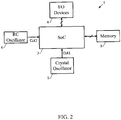
FIG. 2 is a block diagram of an electronic system including a system on a chip that receives its clock signal from a crystal oscillator during normal operations but that receives a clock signal from a RC oscillator during startup operations. -
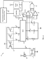
FIG. 3 is a schematic block diagram of the RC oscillator ofFIG. 2 . -
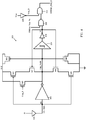
FIG. 4 is a schematic block diagram of the fault detection and reset generation circuit ofFIG. 3 . -
FIG. 5 is a timing diagram of the fault detection and reset generation circuit ofFIG. 4 in operation. -
FIG. 6 is a schematic block diagram of an alternate embodiment of the RC oscillator ofFIG. 2 . -
FIG. 7 is a schematic block diagram of an alternate embodiment of the fault detection and reset generation circuit ofFIG. 3 . - The following disclosure enables a person skilled in the art to make and use the subject matter disclosed herein. The general principles described herein may be applied to embodiments and applications other than those detailed above without departing from the spirit and scope of this disclosure. This disclosure is not intended to be limited to the embodiments shown, but is to be accorded the widest scope consistent with the principles and features disclosed or suggested herein.
- With reference to
FIG. 2 , an embodiment of anelectronic system 1 including a system on a chip (SoC) 2 is now described. TheSoC 2 is coupled to a memory 3, input/output (I/O) devices 4, acrystal oscillator 5, and aRC oscillator 6. When theelectronic system 1 is in a powered state during normal operations, it operates based upon a clock signal CLK1 received from acrystal oscillator 5. - However, when the
electronic system 1 is powered up from a powered down state, theSoC 2 requires a clock signal CLK2 to begin its own startup operations. Thecrystal oscillator 5 takes a relatively long time (on the order of milliseconds) to begin producing the clock signal CLK1 after power up of theelectronic system 1. Therefore, in various embodiments, immediately after power up of theelectronic system 1, theRC oscillator 6 is used to produce a clock signal CLK2 for theSoC 2 because theRC oscillator 6 is able to produce the clock signal CLK2 in a short period of time (on the order of microseconds) after power up. - As explained above, however, standard RC oscillators have undesirable drawbacks that are to be avoided. Therefore, the following design for a
RC oscillator 6 has been developed and will be described with reference toFIG. 3 . - In the embodiment considered, the
RC oscillator 6 includes a current source Gp generating a bias current Ibias. This bias current Ibias is received at the input ofcurrent mirror 7. The output ofcurrent mirror 7 draws current Irif into it, and current Irif is proportional to the bias current Ibias. In the embodiment considered, thecurrent mirror 7 includes (e.g., NMOS) transistor T1 having its drain acting as the input to thecurrent mirror 7, its source coupled to ground, and its gate coupled to its drain. Thecurrent mirror 7 includes (e.g., NMOS) transistor T2 having its drain acting as the output to thecurrent mirror 7, its source coupled to ground, and its gate coupled to the gate of transistor T1. - Current Irif is drawn from the input of current mirror 8. In the embodiment considered, current mirror 8 includes (e.g., PMOS) transistor T3 having its source coupled to supply node Vdd, its drain acting as the input to the current mirror 8, and its gate coupled to its drain. (e.g., PMOS) transistor T4 has its source coupled to the supply node Vdd, its drain coupled to
node 14 to provide output current I1, and its gate coupled to the gate of transistor T3. (e.g., PMOS) transistor T5 has its source coupled to the supply node Vdd, its drain coupled tonode 15 to provide output current 12, and its gate coupled to the gate of transistor T3. (e.g., PMOS) Transistor T6 has it source coupled to the supply node Vdd, its drain coupled tonode 28 to provide output current 13, and its gate coupled to the gate of transistor T3. Thus, the drains of transistor T4, T5, and T6 form the outputs of the current mirror 8. - In the embodiment considered, a
multiplexer 13 has inputs coupled tonodes multiplexer 13 has outputs coupled tonodes - In the embodiment considered, a resistor R is coupled between
node 18 and ground. Capacitor C3 is coupled betweennode 17 and ground, and capacitor C4 is coupled betweennode 16 and ground. - In the embodiment considered, the
multiplexer 13 is controlled by the control signals Ssw received from acontrol circuit 21. - In the embodiment considered, a
comparator 80 has an inverting terminal receiving a reference voltage Vref fromnode 18, a non-inverting terminal receiving voltage V1 fromnode 17, and an output Sc1 coupled to a logic (e.g., OR)gate 84. Acomparator 81 has an inverting terminal receiving the reference voltage Vref fromnode 18, a non-inverting terminal receiving the voltage V2 fromnode 16, and an output Sc2 coupled to the logic (OR)gate 84. - In various embodiments,
comparator 80 is enabled by a comparator enable signal Scomp, andcomparator 81 is enabled by the inverse of the comparator enable signal (e.g., generated by passing Scomp through an inverter 11). - In the embodiment considered, the logic (OR)
gate 84 has its output, producing an output signal Sc, coupled to the inputs of thecontrol circuit 21 and aclock generator 22.Control circuit 21 generates the control signals Ssw as output, andclock generator 22 generates the clock signal CLK2 as output. - In operation, the
current mirror 7 mirrors current Ibias, multiplied by a mirroring factor, to draw current Irif from the input of current mirror 8. The current mirror 8 then mirrors current Irif from its outputs as currents I1, 12, and 13, each being Irif multiplied by a respective mirroring factor. - The
multiplexer 13 is switched between different phases. In various embodiments, in each phase, only one of the capacitors C3 or C4 is supplied by themultiplexer 13, while the other of the capacitors C3 or C4 is allowed to discharge. For example, in a first phase, capacitor C3 is charged while capacitor C4 is allowed to discharge; in a second phase, capacitor C4 is charged while capacitor C3 is allowed to discharge; in a third phase, capacitor C3 is charged while capacitor C4 is allowed to discharge; and in a fourth phase, capacitor C4 is charged while capacitor C3 is allowed to discharge. In each phase where capacitor C3 is charged, one of the currents I1, 12, and I3 is coupled by themultiplexer 13 to the capacitor C3. Likewise, in each phase where the capacitor C4 is charged, one of the currents I1, I2, and I3 is coupled by themultiplexer 13 to the capacitor C4. - When the voltage V1 at
node 17 becomes equal to Vref as the capacitor C3 is charged by one of the currents I1, 12, and 13, thecomparator 80 asserts its output Sc1. This results in the logic (OR)gate 84 asserting its output signal Sc to thecontrol circuit 21 and theclock generator 22. Similarly, when the voltage V2 atnode 16 becomes equal to Vref as the capacitor C4 is charged by one of the currents I1, 12, and 13, thecomparator 81 asserts its output Sc2, resulting in the logic (OR)gate 84 asserting its output signal Sc to thecontrol circuit 21 and theclock generator 22. Thecontrol circuit 21 generates the control signals Ssw and the comparator enable signal Scomp based on the signal Sc, and theclock generator 22 generates the clock signal CLK2 based on the signal Sc. - In various embodiments, when the
RC oscillator 6 is in a powered down state, both of the outputs Sc1 and Sc2 of thecomparators 81 and 82 remain deasserted. When theRC oscillator 6 is powered on, Scomp is asserted, and thecomparator 80 is enabled whilecomparator 81 remains disabled. This results in thecomparator 80 asserting its output Sc1 when the voltage V1 becomes equal to the reference voltage Vref. This results in a rising edge of the signal Sc, and in turn, theclock generator circuit 22 generating a rising edge of the clock signal CLK2. At the same time, this rising edge of the signal Sc results in thecontrol circuit 21 flipping the logic level of Scomp and altering the control signal Ssw to themultiplexer 13. - Altering the control signal Ssw to the
multiplexer 13 changes its configuration so that C3 begins to discharge (V1 falls) and so that C4 begins to charge (V2 rises). When the logic level of Scomp is flipped, thecomparator 80 is disabled, and thecomparator 81 is enabled. When thecomparator 81 is enabled, Vref will be greater than V2, so Sc2 will be deasserted. - V2 rises until it is equal to Vref, at which point the
comparator 81 asserts its output Sc2, resulting in a next rising edge of the signal Sc being generated, and in turn, theclock generator circuit 22 generating a falling edge of the clock signal CLK2. At the same time, this rising edge of the signal Sc results in thecontrol circuit 21 altering the control signal Ssw to themultiplexer 13, which changes its configuration so that C4 begins to discharge (V2 falls), and so that C3 begins to charge (V1 rises). - The repetition of the above steps repeats so as to generate the clock signal CLK2.
- Further specifics of this operation may be found in
U.S. Pat. No. 8,860,517 , entitled "Oscillator circuit and electronic circuit comprising the electronic circuit", the contents of which are hereby incorporated by reference in their entirety. - An alternative arrangement for a RC oscillator 6' is shown in
FIG. 6 . The difference as compared to theRC oscillator 6 ofFIG. 3 is in the comparators 80' and 81', and that instead of theOR gate 84 receiving Sc1 and Sc2 there is aNAND gate 85 receiving those signals. Here, the comparator 80' has its non-inverting terminal coupled to Vref and its inverting terminal coupled to V1, while the comparator 81' has its non-inverting terminal coupled to Vref and its inverting terminal coupled to V2. - In the embodiment considered, when the RC oscillator 6' is in a powered down state, both of the outputs Sc1 and Sc2 of the comparators 81' and 82' remain deasserted. When the RC oscillator 6' is powered on, Scomp is asserted, and the comparator 80' is enabled while comparator 81' remains disabled. Since initially Vref will be greater than V1, the comparator 80' will default to asserting its output Sc1 when initially enabled. When the voltage V1 becomes equal to the reference voltage Vref, the comparator 80' will deassert its output Sc1. Due to the NAND logic from
NANDF gate 85, this results in a rising edge of the signal Sc, and in turn, theclock generator circuit 22 generating a rising edge of the clock signal CLK2. At the same time, this rising edge of the signal Sc results in thecontrol circuit 21 flipping the logic level of the Scomp signal, and altering the control signal Ssw to themultiplexer 13. In response, the multiplexer changes its configuration so that C3 begins to discharge (V1 falls) and C4 begins to charge (V2 rises). When the logic level of Scomp is flipped, the comparator 80' is disabled, and the comparator 81' is enabled. When the comparator 81' is enabled, Vref will be greater than than V2, so Sc2 will be asserted. - V2 rises until it is equal to Vref, at which point the comparator 81' deasserts its output Sc2, resulting in a next rising edge of the signal Sc being generated, and in turn, the
clock generator circuit 22 generating a falling edge of the clock signal CLK2. At the same time, this rising edge of the signal Sc results in thecontrol circuit 21 altering the control signal Ssw to themultiplexer 13, which changes its configuration so that C4 begins to discharge until Sc2 is ultimately re-asserted, and so that C3 begins to charge. The repetition of the above steps repeats so as to generate the clock signal CLK2. - With respect to either the
RC oscillator 6 or the RC oscillator 6', if the edges of the signal Sc are not properly generated, then theclock generator 22 will not change the state of the clock signal CLK2, and the clock signal CLK2 becomes stuck in one state. This results in the startup operations of theSoC 2 failing. - In various embodiments, to detect a fault in the
RC oscillator 6 or 6' where the edges of Sc are not properly generated, a fault detection and resetgeneration circuit 100 is used. Details of an embodiments of the fault detection and resetgeneration circuit 100 are now given with additional reference toFIG. 4 . - In the embodiments considered, the fault detection and reset
generation circuit 100 includes anoptional buffer 101 receiving the signal Sc, and buffering that signal to produce the Clk_Edge signal to node N1. - In the embodiments considered, an
inverter 102 is coupled to node N1 to receive the Clk_Edge signal as input, and provides output to a capacitive node Cap_Node. - In various embodiments, an electronic switch M0 driven as a function of a signal Stop B is connected between the capacitive node Cap_Node and the supply node Vdd (or alternatively ground). For example, in the embodiment considered a (e.g., PMOS) transistor M0 has its source coupled to the supply node Vdd, its drain coupled to the capacitive node Cap_Node, and its gate biased by signal Stop_B. Note that Stop_B is a power down signal.
- In the embodiments considered, two electronic switches M1 and M2 are connected between the capacitive node Cap_Node and the supply node Vdd, wherein the electronic switch M1 is driven via the signal at the node N1 and the electronic switch M2 is driven via the signal at a node N2. For example, in the embodiment considered, a (e.g., PMOS) transistor M1 has its source coupled to the supply node Vdd, a drain, and its gate coupled to node N1 to be biased by the Clk_Edge signal. A (e.g. PMOS) transistor M2 has its source coupled to the drain of transistor M1, its drain coupled to the capacitive node Cap_Node, and a gate coupled to node N2.
- In the embodiments considered, two electronic switches M4 and M5 are connected between the capacitive node Cap_Node and ground, wherein the electronic switch M4 is driven via the signal at the node N2 and the electronic switch MM is driven via the signal at the node N1. For example, in the embodiments considered, an (e.g. NMOS) transistor M4 has its drain coupled to the capacitive node Cap_Node, a source, and a gate coupled to node N2. An (e.g. NMOS) transistor M5 has its drain coupled to the source of transistor M4, its source coupled to ground, and its gate coupled to node N1 to be biased by the Clk_Edge signal.
- In various embodiments, capacitators M3 and M6 are connected between the capacitive node Cap_Node, and the supply node Vdd and ground, respectively. For example, in the embodiment considered, a (e.g. PMOS) transistor M3 has its source and drain coupled to the supply node Vdd and its gate coupled to the capacitive node Cap Node. Thus, the source and drain of the transistor M3 act as one plate of a capacitor and the gate of the transistor M3 acts as the other plate of the capacitor. Similarly, a (e.g. PMOS) transistor M6 has its source and drain coupled to the ground node and its gate coupled to the capacitive node Cap_Node. Likewise here, the source and drain of the transistor M6 act as one plate of a capacitor and the gate of the transistor acts as the other plate of the capacitor.
- In the embodiment considered, a
Schmitt trigger 104 has its input coupled to the capacitive node Cap_Node, and provides its output to node N2 throughinverter 106. - In various embodiments, a logic (e.g. NAND)
gate 108 has inputs coupled to node N2 and to a CLkMon_Stop_En signal. Note that the ClkMon_Stop_En signal acts as an enable signal for the logic (NAND)gate 108. - In various embodiments, a logic (e.g. AND)
gate 112 has an input coupled to the output of the logic (NAND)gate 108, and to the output of aninverter 110. In the embodiments considered, theinverter 110 receives a Stop signal, inverts it, and passes the inverted Stop signal to the logic (AND)gate 112. Note that the Stop signal, when high, serves to pull the output of the logic (AND)gate 112 low. The ClkMon_Stop_B signal is generated at the output of the logic (AND)gate 112. - Accordingly, in general, the
logic gates - In operation, when the signal Sc is low, the
inverter 102 charges the capacitive node Cap_Node to a logic high. When Sc transitions high, and theinverter 102 then works to discharge the capacitive node Cap_Node over time. - During correct operation of the
RC oscillator 6, the signal Sc (and therefore Clk_Edge) only stays at a logic high for a short period of time during a single period of the clock CLK2, and remains at a logic low the remainder of the period of the clock CLK2. However, if the error condition described above occurs in which the signal Sc fails to transition, the signal Sc will remain at a logic high. - This results in the
inverter 102 discharging the capacitive node Cap_Node below a threshold such that the Schmitt trigger 104 trips and asserts its output as a logic high. This ultimately results in the combinational logic circuit (e.g., the AND gate 112) generating the ClkMon_Stop_B signal as a logic zero, generating a reset signal for theRC oscillator 6. - In various embodiments, the reset signal for the
RC oscillator 6 serves to reset the signal Sc to a logic low. As explained above, the effect on the fault generation and resetgeneration circuit 100 of the signal Sc being at a logic low is to begin to charge the capacitive node Cap_Node. Once the voltage at the capacitive node Cap_Node is equal to the threshold, the Schmitt trigger triggers and asserts its output as a logic low. This ultimately results in the ClkMon_Stop_B signal being asserted by the combinational logic circuit (e.g., the AND gate 112) at a logic high, and the restart of theRC oscillator 6 into a normal mode of operation. - In the embodiments considered, the optional transistor M1 and M2 are arranged as a latch that serves to help the
inverter 102 pull the capacitive node Cap_Node high while the signal Sc is low, and the optional transistor M4 and M5 are likewise arranged as a latch that serves to help theinverter 102 pull the capacitive node Cap_Node low while the signal Sc is high. - In greater detail, transistor M1 is enabled when Clk_Edge is at a logic low. The feedback from transistor M2 forms the latch, pulling the capacitive node Cap_Node high when node N2 is at a logic low. Transistor M5 is enabled when Clk_Edge is at a logic high. The feedback from transistor M4 forms the latch, pulling the capacitive node Cap_Node low when node N2 is at a logic low. Therefore, the latch is dependent on the states of Clk_Edge and N2.
- Operation of the fault detection and reset
generation circuit 100 can be seen in the timing diagram ofFIG. 5 . It can be seen that during time period t0, theRC oscillator 6 is operating properly, andcomparators OR gate 84 is transitioning properly, with the signal Sc remaining only briefly at logic highs. Accordingly, since the signal Sc is only briefly at logic highs, the capacitance of the capacitance node Cap_Node filters those spikes, so the capacitive node Cap_Node remains at a logic high during period t0. Accordingly, theSchmitt trigger 104 does not trip, and its output remains deasserted at a logic low, resulting in the ClkMon_Stop_B signal remaining at a logic high, as seen during period t0. Thus, during time period t0, the clock signal CLK2 runs properly. - At the beginning of time period t1, however, operation of the
RC oscillator 6 becomes stuck, with the output Sc1 of thecomparator 80 becoming stuck at a logic low, and the output Sc2 of thecomparator 81 becoming stuck at a logic high. Resultingly, the output signal Sc from theOR gate 84 becomes stuck at a logic high, and the clock signal CLK2 is stuck at a logic high. - As explained, this results in the
inverter 102 and latch formed from transistors M4-M5 discharging the capacitive node Cap_Node until, at the beginning of time period t2, theSchmitt trigger 104 resultingly trips and asserts its output at a logic high, resulting in the ClkMon_Stop_B signal being pulled to a logic low. The ClkMon_Stop_B signal remains at a logic low during time period t2, generating the reset signal for theRC oscillator 6. - The reset signal for the
RC oscillator 6 resets the signal Sc to a logic low, and thus, at the beginning of time period t3, the capacitive node Cap_Node begins to be charge up again via theinverter 102 and the latch formed from transistors M1-M2. Once the voltage at the capacitive node Cap_Node is equal to a threshold value at the beginning of time period t4, theSchmitt trigger 104 triggers and asserts its output as a logic low. This results in the ClkMon_Stop_B signal being asserted at a logic high, and the restart of theRC oscillator 6 into a normal mode of operation. Thus, due to the reset, at the beginning of time period t4, the clock signal CLK2 begins to run properly again. - Note that the capacitive node Cap_Node may have equal charge and discharge times, or may in some instances have asymmetric charge and discharge times so as to reduce the wake-up time of the
RC oscillator 6. - In some instances, it may be desirable to invert the output of the fault detection and reset
generation circuit 100, making the ClkMon_Stop_B signal a high signal when an error is detected. - An alternative fault detection and reset generation circuit 100' is shown in
FIG.7 . The difference between the fault detection and resetgeneration circuit 100 ofFIG. 4 and the fault detection and reset generation circuit 100' ofFIG. 7 is that fault detection and reset generation circuit 100' has itsinverter 102 powered through adjustable current sources I1 and 12, which enable control of wake-up and reset times for the fault detection and reset generation circuit 100'. - While the disclosure has been described with respect to a limited number of embodiments, those skilled in the art, having benefit of this disclosure, will appreciate that other embodiments can be envisioned that do not depart from the scope of the disclosure as disclosed herein. Accordingly, the scope of the disclosure shall be limited only by the attached claims. For example, while reference has been made mainly to NMOS and PMOS transistors, such transistors may also be replaced with other n-channel or p-channel Field Effect Transistors, respectively.
Claims (16)
- A circuit, comprising:an RC oscillator (6; 6') comprising:a first comparison circuit (80; 80'),a second comparison circuit (81; 81'),a logic circuit (84; 85) receiving output from the first and second comparison circuits as input, and generating a logic output signal, anda clock generation circuit (22) generating a clock signal as a function of the logic output signal (Sc); andan oscillator fault detection circuit (100; 100') comprising:a capacitive node (Cap_Node),charge circuitry (102, M1, M2) configured to selectively charge the capacitive node (Cap_Node) based upon the logic output signal (Sc, N1),discharge circuitry (102, M4, M5) configured to selectively discharge the capacitive node (Cap_Node) based upon the logic output signal (Sc, N1), andtriggering circuitry (104, 106, 108, 110, 112) configured to assert a reset signal (ClkMon_Stop_B) when the charge on the capacitive node (Cap_Node) indicates a fault with the RC oscillator.
- The circuit of claim 1, wherein the discharge circuitry (102, M4, M5) fails to discharge the capacitive node (Cap_Node) to a lower threshold when the logic output signal (Sc, N1) transitions in a pattern indicating proper operation of the RC oscillator; and wherein the charge on the capacitive node (Cap_Node) being above the lower threshold indicates proper operation of the RC oscillator.
- The circuit of claim 1 or claim 2, wherein the discharge circuitry (102, M4, M5) begins to discharges the capacitive node (Cap_Node) to below a lower threshold when the logic output signal (Sc, N1) fails to transition in a pattern indicating proper operation of the RC oscillator; and wherein the charge on the capacitive node (Cap Node) being below the lower threshold indicates a fault with the RC oscillator.
- The circuit of any of the previous claims, wherein the charge circuitry (102, M1, M2) maintains the capacitive node (Cap_Node) above a lower threshold when the logic output signal (Sc, N1) transitions in a pattern indicating proper operation of the RC oscillator; and wherein charge on the capacitive node (Cap Node) being above an upper threshold indicates proper operation of the RC oscillator.
- The circuit of claim 4, wherein the reset signal (ClkMon_Stop_B) serves to reset the RC oscillator such that the RC oscillator returns to proper operation; and wherein the charge circuitry (102, M1, M2) charges the capacitive node (Cap_Node) to back above the lower threshold when the logic output signal (Sc, N1) returns to a reset state after the RC oscillator has been reset by the reset signal (ClkMon_Stop_B), thereby resulting in the triggering circuitry (104, 106, 108, 110, 112) deasserting the reset signal (ClkMon_Stop_B).
- The circuit of any of the previous claims, wherein the charge circuitry (102, M1, M2) does not charge the capacitive node (Cap_Node) when the logic output signal (Sc, N1) fails to transition in a pattern indicating proper operation of the RC oscillator.
- The circuit of any of the previous claims, wherein the charge circuitry (102, M1, M2) comprises an inverter (102) coupled to receive the logic output signal (Sc) and provide output to the capacitive node (Cap_Node); and wherein the discharge circuitry (102, M4, M5) also comprises the inverter (102).
- The circuit of claim 7, wherein the oscillator fault detection circuit further comprises a buffer (101) coupled between the logic output signal (Sc) and the inverter (102).
- The circuit of any of the previous claims, wherein the triggering circuitry comprises a Schmitt trigger (104) having an input coupled to the capacitive node.
- The circuit of 9, wherein at least one inverter (106) is coupled between an output of the Schmitt trigger (102) and an output of the oscillator fault detection circuit (100; 100').
- The circuit of claim 7 and 9, wherein the charge circuitry (102, M1, M2) further comprises a first latch (M1, M2); and wherein the discharge circuitry (102, M4, M5) further comprising a second latch (M4, M5).
- The circuit of claim 11, wherein the first latch (M1, M2) comprises:a first PMOS transistor (M1) having a source coupled to a supply node (Vdd), a drain, and a gate coupled to the logic output signal (Sc, N1); anda second PMOS transistor (M2) having a source coupled to the drain of the first PMOS transistor (M1), a drain coupled to the capacitive node (Camp_Node), and a gate coupled to the output of the Schmitt trigger (104).
- The circuit of claim 11 or claim 12, wherein the second latch (M4, M5) comprises:a first NMOS transistor (M4) having a drain coupled to the capacitive node (Cap_Node), a source, and a gate coupled to the output of the Schmitt trigger (104); anda second NMOS transistor (M5) having a drain coupled to the source of the first NMOS transistor (M4), a source coupled to ground, and a gate coupled to the logic output signal (Sc, N1).
- The circuit of any of the previous claims, wherein the capacitive node (Cap_Node) is coupled to at least one field effect transistor (M3, M6) configured as a capacitor.
- The circuit of claim 14, wherein the at least one field effect transistor (M3, M6) comprises:a first, e.g. PMOS, transistor (M3) having a source and drain coupled to a supply node (Vdd) and a gate coupled to the capacitive node (Cap_Node); anda second, e.g. PMOS, transistor (M6) having a source and drain coupled to ground and a gate coupled to the capacitive node (Cap_Node).
- The circuit of any of the previous claims, wherein the first comparison circuit (80; 80') comprises a first comparator, wherein the second comparison circuit (81; 81') comprises a second comparator, and wherein the logic circuit (84; 85) comprises an OR gate.
Applications Claiming Priority (1)
| Application Number | Priority Date | Filing Date | Title |
|---|---|---|---|
| US16/027,762 US10680587B2 (en) | 2018-07-05 | 2018-07-05 | RC oscillator watchdog circuit |
Publications (2)
| Publication Number | Publication Date |
|---|---|
| EP3591842A1 true EP3591842A1 (en) | 2020-01-08 |
| EP3591842B1 EP3591842B1 (en) | 2021-01-27 |
Family
ID=67180597
Family Applications (1)
| Application Number | Title | Priority Date | Filing Date |
|---|---|---|---|
| EP19184330.9A Active EP3591842B1 (en) | 2018-07-05 | 2019-07-04 | Rc oscillator watchdog circuit |
Country Status (2)
| Country | Link |
|---|---|
| US (1) | US10680587B2 (en) |
| EP (1) | EP3591842B1 (en) |
Families Citing this family (6)
| Publication number | Priority date | Publication date | Assignee | Title |
|---|---|---|---|---|
| EP3930191A1 (en) * | 2020-06-25 | 2021-12-29 | ams International AG | Oscillator circuit, device and method for generating an oscillator signal |
| CN112084054B (en) * | 2020-08-17 | 2024-12-03 | 浪潮网络科技(山东)有限公司 | A watchdog circuit and a dog feeding method and device |
| US11796606B2 (en) | 2021-04-20 | 2023-10-24 | Texas Instruments Incorporated | Pin-leakage compensation scheme for external resistor-based oscillators |
| US11848645B2 (en) | 2021-04-22 | 2023-12-19 | Texas Instruments Incorporated | Enabling an external resistor for an oscillator |
| US11437955B1 (en) | 2021-08-05 | 2022-09-06 | Texas Instruments Incorporated | Switchover schemes for transition of oscillator from internal-resistor to external-resistor mode |
| US11764728B1 (en) * | 2022-04-14 | 2023-09-19 | Airoha Technology Corp. | Oscillator using chopper circuit for suppressing flicker noise of current sources and associated clock generation method |
Citations (6)
| Publication number | Priority date | Publication date | Assignee | Title |
|---|---|---|---|---|
| JPH0794942A (en) * | 1993-09-09 | 1995-04-07 | Fujitsu Ltd | Reference clock signal generation circuit |
| US5565819A (en) * | 1995-07-11 | 1996-10-15 | Microchip Technology Incorporated | Accurate RC oscillator having modified threshold voltages |
| US20070188904A1 (en) * | 2006-02-16 | 2007-08-16 | Fujitsu Limited | Output control device and recording-medium-driver control device |
| US20110320852A1 (en) * | 2010-06-23 | 2011-12-29 | Novatek Microelectronics Corp. | Clock circuit and reset circuit and method thereof |
| US8860517B2 (en) | 2011-06-27 | 2014-10-14 | Stmicroelectronics S.R.L. | Oscillator circut and electronic circuit comprising the oscillator circuit |
| US20180054163A1 (en) * | 2016-08-18 | 2018-02-22 | M2Communication Inc. | Method of monitoring clock and oscillator module thereof |
Family Cites Families (8)
| Publication number | Priority date | Publication date | Assignee | Title |
|---|---|---|---|---|
| US5594388A (en) | 1995-06-07 | 1997-01-14 | American Microsystems, Inc. | Self-calibrating RC oscillator |
| US6668334B1 (en) * | 2000-06-27 | 2003-12-23 | Lucent Technologies Inc. | Apparatus for detecting clock failure within a fixed number of cycles of the clock |
| US6707320B2 (en) * | 2001-11-30 | 2004-03-16 | Sun Microsystems, Inc. | Clock detect indicator |
| JP3937888B2 (en) * | 2002-03-27 | 2007-06-27 | ヤマハ株式会社 | Oscillation detection circuit |
| US7498848B2 (en) * | 2006-10-03 | 2009-03-03 | Freescale Semiconductor, Inc. | System and method for monitoring clock signal in an integrated circuit |
| US8456243B2 (en) * | 2010-03-26 | 2013-06-04 | Microchip Technology Incorporated | Failsafe oscillator monitor and alarm |
| US20150234420A1 (en) * | 2014-02-18 | 2015-08-20 | Energy Pass Incorporation | Clock Switching Circuit |
| WO2016119139A1 (en) | 2015-01-28 | 2016-08-04 | Texas Instruments Incorporated | Fault detection and self-recovery method for crystal oscillator |
-
2018
- 2018-07-05 US US16/027,762 patent/US10680587B2/en active Active
-
2019
- 2019-07-04 EP EP19184330.9A patent/EP3591842B1/en active Active
Patent Citations (6)
| Publication number | Priority date | Publication date | Assignee | Title |
|---|---|---|---|---|
| JPH0794942A (en) * | 1993-09-09 | 1995-04-07 | Fujitsu Ltd | Reference clock signal generation circuit |
| US5565819A (en) * | 1995-07-11 | 1996-10-15 | Microchip Technology Incorporated | Accurate RC oscillator having modified threshold voltages |
| US20070188904A1 (en) * | 2006-02-16 | 2007-08-16 | Fujitsu Limited | Output control device and recording-medium-driver control device |
| US20110320852A1 (en) * | 2010-06-23 | 2011-12-29 | Novatek Microelectronics Corp. | Clock circuit and reset circuit and method thereof |
| US8860517B2 (en) | 2011-06-27 | 2014-10-14 | Stmicroelectronics S.R.L. | Oscillator circut and electronic circuit comprising the oscillator circuit |
| US20180054163A1 (en) * | 2016-08-18 | 2018-02-22 | M2Communication Inc. | Method of monitoring clock and oscillator module thereof |
Also Published As
| Publication number | Publication date |
|---|---|
| US10680587B2 (en) | 2020-06-09 |
| EP3591842B1 (en) | 2021-01-27 |
| US20200014372A1 (en) | 2020-01-09 |
Similar Documents
| Publication | Publication Date | Title |
|---|---|---|
| EP3591842B1 (en) | Rc oscillator watchdog circuit | |
| US6720673B2 (en) | Voltage island fencing | |
| US8164357B2 (en) | Digital noise protection circuit and method | |
| JP6174276B1 (en) | Delay structure for memory interface | |
| US10587253B1 (en) | Ring oscillator-based programmable delay line | |
| US9443572B2 (en) | Programmable power for a memory interface | |
| JP2011223375A (en) | Oscillator circuit | |
| US6388479B1 (en) | Oscillator based power-on-reset circuit | |
| KR950010208B1 (en) | Phase-locked loop clock signal generator | |
| KR20010044877A (en) | Analog-digital mixed type delay locked loop combining voltage controlled oscillator and shift register type delay locked loop | |
| KR20120121685A (en) | Semiconductor device and delay locked loop circuit of semiconductor device | |
| JP7542748B2 (en) | RC Oscillator Circuit | |
| US10727820B2 (en) | Power- and area-efficient clock detector | |
| US6518848B2 (en) | Oscillation stop detection circuit | |
| CN118295857A (en) | Clock circuit | |
| KR20160149717A (en) | Semiconductor device and operating method thereof | |
| US10038372B2 (en) | Method and device for controlling a charge pump circuit | |
| US7705685B2 (en) | Low-voltage oscillator with capacitor-ratio selectable duty cycle | |
| JPH10190416A (en) | Flip-flop circuit | |
| US10734949B2 (en) | Self enabling signal conditioner for conditioning a crystal oscillator output signal into a compliant clock signal | |
| US10879882B1 (en) | Low-power fast-setting delay circuit | |
| JP2000013206A (en) | Clock monitor circuit and synchronous semiconductor memory device | |
| KR0168079B1 (en) | Clock generating apparatus | |
| US8319525B2 (en) | Flip-flop circuit and leakage current suppression circuit utilized in a flip-flop circuit | |
| US6911873B2 (en) | Detection circuit and method for an oscillator |
Legal Events
| Date | Code | Title | Description |
|---|---|---|---|
| PUAI | Public reference made under article 153(3) epc to a published international application that has entered the european phase |
Free format text: ORIGINAL CODE: 0009012 |
|
| STAA | Information on the status of an ep patent application or granted ep patent |
Free format text: STATUS: THE APPLICATION HAS BEEN PUBLISHED |
|
| AK | Designated contracting states |
Kind code of ref document: A1 Designated state(s): AL AT BE BG CH CY CZ DE DK EE ES FI FR GB GR HR HU IE IS IT LI LT LU LV MC MK MT NL NO PL PT RO RS SE SI SK SM TR |
|
| AX | Request for extension of the european patent |
Extension state: BA ME |
|
| STAA | Information on the status of an ep patent application or granted ep patent |
Free format text: STATUS: REQUEST FOR EXAMINATION WAS MADE |
|
| 17P | Request for examination filed |
Effective date: 20200701 |
|
| RBV | Designated contracting states (corrected) |
Designated state(s): AL AT BE BG CH CY CZ DE DK EE ES FI FR GB GR HR HU IE IS IT LI LT LU LV MC MK MT NL NO PL PT RO RS SE SI SK SM TR |
|
| GRAP | Despatch of communication of intention to grant a patent |
Free format text: ORIGINAL CODE: EPIDOSNIGR1 |
|
| STAA | Information on the status of an ep patent application or granted ep patent |
Free format text: STATUS: GRANT OF PATENT IS INTENDED |
|
| INTG | Intention to grant announced |
Effective date: 20200918 |
|
| GRAS | Grant fee paid |
Free format text: ORIGINAL CODE: EPIDOSNIGR3 |
|
| GRAA | (expected) grant |
Free format text: ORIGINAL CODE: 0009210 |
|
| STAA | Information on the status of an ep patent application or granted ep patent |
Free format text: STATUS: THE PATENT HAS BEEN GRANTED |
|
| AK | Designated contracting states |
Kind code of ref document: B1 Designated state(s): AL AT BE BG CH CY CZ DE DK EE ES FI FR GB GR HR HU IE IS IT LI LT LU LV MC MK MT NL NO PL PT RO RS SE SI SK SM TR |
|
| REG | Reference to a national code |
Ref country code: GB Ref legal event code: FG4D |
|
| REG | Reference to a national code |
Ref country code: CH Ref legal event code: EP |
|
| REG | Reference to a national code |
Ref country code: AT Ref legal event code: REF Ref document number: 1359250 Country of ref document: AT Kind code of ref document: T Effective date: 20210215 |
|
| REG | Reference to a national code |
Ref country code: IE Ref legal event code: FG4D |
|
| REG | Reference to a national code |
Ref country code: DE Ref legal event code: R096 Ref document number: 602019002358 Country of ref document: DE |
|
| REG | Reference to a national code |
Ref country code: NL Ref legal event code: MP Effective date: 20210127 |
|
| REG | Reference to a national code |
Ref country code: LT Ref legal event code: MG9D |
|
| REG | Reference to a national code |
Ref country code: AT Ref legal event code: MK05 Ref document number: 1359250 Country of ref document: AT Kind code of ref document: T Effective date: 20210127 |
|
| PG25 | Lapsed in a contracting state [announced via postgrant information from national office to epo] |
Ref country code: GR Free format text: LAPSE BECAUSE OF FAILURE TO SUBMIT A TRANSLATION OF THE DESCRIPTION OR TO PAY THE FEE WITHIN THE PRESCRIBED TIME-LIMIT Effective date: 20210428 Ref country code: FI Free format text: LAPSE BECAUSE OF FAILURE TO SUBMIT A TRANSLATION OF THE DESCRIPTION OR TO PAY THE FEE WITHIN THE PRESCRIBED TIME-LIMIT Effective date: 20210127 Ref country code: HR Free format text: LAPSE BECAUSE OF FAILURE TO SUBMIT A TRANSLATION OF THE DESCRIPTION OR TO PAY THE FEE WITHIN THE PRESCRIBED TIME-LIMIT Effective date: 20210127 Ref country code: BG Free format text: LAPSE BECAUSE OF FAILURE TO SUBMIT A TRANSLATION OF THE DESCRIPTION OR TO PAY THE FEE WITHIN THE PRESCRIBED TIME-LIMIT Effective date: 20210427 Ref country code: LT Free format text: LAPSE BECAUSE OF FAILURE TO SUBMIT A TRANSLATION OF THE DESCRIPTION OR TO PAY THE FEE WITHIN THE PRESCRIBED TIME-LIMIT Effective date: 20210127 Ref country code: NO Free format text: LAPSE BECAUSE OF FAILURE TO SUBMIT A TRANSLATION OF THE DESCRIPTION OR TO PAY THE FEE WITHIN THE PRESCRIBED TIME-LIMIT Effective date: 20210427 Ref country code: PT Free format text: LAPSE BECAUSE OF FAILURE TO SUBMIT A TRANSLATION OF THE DESCRIPTION OR TO PAY THE FEE WITHIN THE PRESCRIBED TIME-LIMIT Effective date: 20210527 |
|
| PG25 | Lapsed in a contracting state [announced via postgrant information from national office to epo] |
Ref country code: LV Free format text: LAPSE BECAUSE OF FAILURE TO SUBMIT A TRANSLATION OF THE DESCRIPTION OR TO PAY THE FEE WITHIN THE PRESCRIBED TIME-LIMIT Effective date: 20210127 Ref country code: PL Free format text: LAPSE BECAUSE OF FAILURE TO SUBMIT A TRANSLATION OF THE DESCRIPTION OR TO PAY THE FEE WITHIN THE PRESCRIBED TIME-LIMIT Effective date: 20210127 Ref country code: AT Free format text: LAPSE BECAUSE OF FAILURE TO SUBMIT A TRANSLATION OF THE DESCRIPTION OR TO PAY THE FEE WITHIN THE PRESCRIBED TIME-LIMIT Effective date: 20210127 Ref country code: RS Free format text: LAPSE BECAUSE OF FAILURE TO SUBMIT A TRANSLATION OF THE DESCRIPTION OR TO PAY THE FEE WITHIN THE PRESCRIBED TIME-LIMIT Effective date: 20210127 Ref country code: SE Free format text: LAPSE BECAUSE OF FAILURE TO SUBMIT A TRANSLATION OF THE DESCRIPTION OR TO PAY THE FEE WITHIN THE PRESCRIBED TIME-LIMIT Effective date: 20210127 |
|
| PG25 | Lapsed in a contracting state [announced via postgrant information from national office to epo] |
Ref country code: IS Free format text: LAPSE BECAUSE OF FAILURE TO SUBMIT A TRANSLATION OF THE DESCRIPTION OR TO PAY THE FEE WITHIN THE PRESCRIBED TIME-LIMIT Effective date: 20210527 |
|
| REG | Reference to a national code |
Ref country code: DE Ref legal event code: R097 Ref document number: 602019002358 Country of ref document: DE |
|
| PG25 | Lapsed in a contracting state [announced via postgrant information from national office to epo] |
Ref country code: EE Free format text: LAPSE BECAUSE OF FAILURE TO SUBMIT A TRANSLATION OF THE DESCRIPTION OR TO PAY THE FEE WITHIN THE PRESCRIBED TIME-LIMIT Effective date: 20210127 Ref country code: CZ Free format text: LAPSE BECAUSE OF FAILURE TO SUBMIT A TRANSLATION OF THE DESCRIPTION OR TO PAY THE FEE WITHIN THE PRESCRIBED TIME-LIMIT Effective date: 20210127 Ref country code: SM Free format text: LAPSE BECAUSE OF FAILURE TO SUBMIT A TRANSLATION OF THE DESCRIPTION OR TO PAY THE FEE WITHIN THE PRESCRIBED TIME-LIMIT Effective date: 20210127 |
|
| PG25 | Lapsed in a contracting state [announced via postgrant information from national office to epo] |
Ref country code: DK Free format text: LAPSE BECAUSE OF FAILURE TO SUBMIT A TRANSLATION OF THE DESCRIPTION OR TO PAY THE FEE WITHIN THE PRESCRIBED TIME-LIMIT Effective date: 20210127 Ref country code: SK Free format text: LAPSE BECAUSE OF FAILURE TO SUBMIT A TRANSLATION OF THE DESCRIPTION OR TO PAY THE FEE WITHIN THE PRESCRIBED TIME-LIMIT Effective date: 20210127 Ref country code: RO Free format text: LAPSE BECAUSE OF FAILURE TO SUBMIT A TRANSLATION OF THE DESCRIPTION OR TO PAY THE FEE WITHIN THE PRESCRIBED TIME-LIMIT Effective date: 20210127 |
|
| PLBE | No opposition filed within time limit |
Free format text: ORIGINAL CODE: 0009261 |
|
| STAA | Information on the status of an ep patent application or granted ep patent |
Free format text: STATUS: NO OPPOSITION FILED WITHIN TIME LIMIT |
|
| 26N | No opposition filed |
Effective date: 20211028 |
|
| PG25 | Lapsed in a contracting state [announced via postgrant information from national office to epo] |
Ref country code: AL Free format text: LAPSE BECAUSE OF FAILURE TO SUBMIT A TRANSLATION OF THE DESCRIPTION OR TO PAY THE FEE WITHIN THE PRESCRIBED TIME-LIMIT Effective date: 20210127 Ref country code: ES Free format text: LAPSE BECAUSE OF FAILURE TO SUBMIT A TRANSLATION OF THE DESCRIPTION OR TO PAY THE FEE WITHIN THE PRESCRIBED TIME-LIMIT Effective date: 20210127 |
|
| PG25 | Lapsed in a contracting state [announced via postgrant information from national office to epo] |
Ref country code: SI Free format text: LAPSE BECAUSE OF FAILURE TO SUBMIT A TRANSLATION OF THE DESCRIPTION OR TO PAY THE FEE WITHIN THE PRESCRIBED TIME-LIMIT Effective date: 20210127 |
|
| PG25 | Lapsed in a contracting state [announced via postgrant information from national office to epo] |
Ref country code: MC Free format text: LAPSE BECAUSE OF FAILURE TO SUBMIT A TRANSLATION OF THE DESCRIPTION OR TO PAY THE FEE WITHIN THE PRESCRIBED TIME-LIMIT Effective date: 20210127 |
|
| REG | Reference to a national code |
Ref country code: BE Ref legal event code: MM Effective date: 20210731 |
|
| PG25 | Lapsed in a contracting state [announced via postgrant information from national office to epo] |
Ref country code: IT Free format text: LAPSE BECAUSE OF FAILURE TO SUBMIT A TRANSLATION OF THE DESCRIPTION OR TO PAY THE FEE WITHIN THE PRESCRIBED TIME-LIMIT Effective date: 20210127 |
|
| PG25 | Lapsed in a contracting state [announced via postgrant information from national office to epo] |
Ref country code: IS Free format text: LAPSE BECAUSE OF FAILURE TO SUBMIT A TRANSLATION OF THE DESCRIPTION OR TO PAY THE FEE WITHIN THE PRESCRIBED TIME-LIMIT Effective date: 20210527 Ref country code: LU Free format text: LAPSE BECAUSE OF NON-PAYMENT OF DUE FEES Effective date: 20210704 Ref country code: FR Free format text: LAPSE BECAUSE OF NON-PAYMENT OF DUE FEES Effective date: 20210731 |
|
| PG25 | Lapsed in a contracting state [announced via postgrant information from national office to epo] |
Ref country code: IE Free format text: LAPSE BECAUSE OF NON-PAYMENT OF DUE FEES Effective date: 20210704 Ref country code: BE Free format text: LAPSE BECAUSE OF NON-PAYMENT OF DUE FEES Effective date: 20210731 |
|
| REG | Reference to a national code |
Ref country code: CH Ref legal event code: PL |
|
| PG25 | Lapsed in a contracting state [announced via postgrant information from national office to epo] |
Ref country code: LI Free format text: LAPSE BECAUSE OF NON-PAYMENT OF DUE FEES Effective date: 20220731 Ref country code: CH Free format text: LAPSE BECAUSE OF NON-PAYMENT OF DUE FEES Effective date: 20220731 |
|
| PG25 | Lapsed in a contracting state [announced via postgrant information from national office to epo] |
Ref country code: NL Free format text: LAPSE BECAUSE OF NON-PAYMENT OF DUE FEES Effective date: 20210127 Ref country code: CY Free format text: LAPSE BECAUSE OF FAILURE TO SUBMIT A TRANSLATION OF THE DESCRIPTION OR TO PAY THE FEE WITHIN THE PRESCRIBED TIME-LIMIT Effective date: 20210127 |
|
| PG25 | Lapsed in a contracting state [announced via postgrant information from national office to epo] |
Ref country code: HU Free format text: LAPSE BECAUSE OF FAILURE TO SUBMIT A TRANSLATION OF THE DESCRIPTION OR TO PAY THE FEE WITHIN THE PRESCRIBED TIME-LIMIT; INVALID AB INITIO Effective date: 20190704 |
|
| GBPC | Gb: european patent ceased through non-payment of renewal fee |
Effective date: 20230704 |
|
| PG25 | Lapsed in a contracting state [announced via postgrant information from national office to epo] |
Ref country code: MK Free format text: LAPSE BECAUSE OF FAILURE TO SUBMIT A TRANSLATION OF THE DESCRIPTION OR TO PAY THE FEE WITHIN THE PRESCRIBED TIME-LIMIT Effective date: 20210127 Ref country code: GB Free format text: LAPSE BECAUSE OF NON-PAYMENT OF DUE FEES Effective date: 20230704 |
|
| PG25 | Lapsed in a contracting state [announced via postgrant information from national office to epo] |
Ref country code: MT Free format text: LAPSE BECAUSE OF FAILURE TO SUBMIT A TRANSLATION OF THE DESCRIPTION OR TO PAY THE FEE WITHIN THE PRESCRIBED TIME-LIMIT Effective date: 20210127 |
|
| PGFP | Annual fee paid to national office [announced via postgrant information from national office to epo] |
Ref country code: DE Payment date: 20250620 Year of fee payment: 7 |
|
| PG25 | Lapsed in a contracting state [announced via postgrant information from national office to epo] |
Ref country code: TR Free format text: LAPSE BECAUSE OF FAILURE TO SUBMIT A TRANSLATION OF THE DESCRIPTION OR TO PAY THE FEE WITHIN THE PRESCRIBED TIME-LIMIT Effective date: 20210127 |