EP3591285B1 - Lighting device - Google Patents
Lighting device Download PDFInfo
- Publication number
- EP3591285B1 EP3591285B1 EP19176108.9A EP19176108A EP3591285B1 EP 3591285 B1 EP3591285 B1 EP 3591285B1 EP 19176108 A EP19176108 A EP 19176108A EP 3591285 B1 EP3591285 B1 EP 3591285B1
- Authority
- EP
- European Patent Office
- Prior art keywords
- light
- light source
- reflection
- disposed
- resin layer
- Prior art date
- Legal status (The legal status is an assumption and is not a legal conclusion. Google has not performed a legal analysis and makes no representation as to the accuracy of the status listed.)
- Active
Links
Images





Classifications
-
- F—MECHANICAL ENGINEERING; LIGHTING; HEATING; WEAPONS; BLASTING
- F21—LIGHTING
- F21V—FUNCTIONAL FEATURES OR DETAILS OF LIGHTING DEVICES OR SYSTEMS THEREOF; STRUCTURAL COMBINATIONS OF LIGHTING DEVICES WITH OTHER ARTICLES, NOT OTHERWISE PROVIDED FOR
- F21V3/00—Globes; Bowls; Cover glasses
- F21V3/02—Globes; Bowls; Cover glasses characterised by the shape
-
- F—MECHANICAL ENGINEERING; LIGHTING; HEATING; WEAPONS; BLASTING
- F21—LIGHTING
- F21S—NON-PORTABLE LIGHTING DEVICES; SYSTEMS THEREOF; VEHICLE LIGHTING DEVICES SPECIALLY ADAPTED FOR VEHICLE EXTERIORS
- F21S41/00—Illuminating devices specially adapted for vehicle exteriors, e.g. headlamps
- F21S41/20—Illuminating devices specially adapted for vehicle exteriors, e.g. headlamps characterised by refractors, transparent cover plates, light guides or filters
-
- B—PERFORMING OPERATIONS; TRANSPORTING
- B60—VEHICLES IN GENERAL
- B60Q—ARRANGEMENT OF SIGNALLING OR LIGHTING DEVICES, THE MOUNTING OR SUPPORTING THEREOF OR CIRCUITS THEREFOR, FOR VEHICLES IN GENERAL
- B60Q1/00—Arrangement of optical signalling or lighting devices, the mounting or supporting thereof or circuits therefor
- B60Q1/0011—Arrangement of optical signalling or lighting devices, the mounting or supporting thereof or circuits therefor with light guides for distributing the light between several lighting or signalling devices
-
- F—MECHANICAL ENGINEERING; LIGHTING; HEATING; WEAPONS; BLASTING
- F21—LIGHTING
- F21S—NON-PORTABLE LIGHTING DEVICES; SYSTEMS THEREOF; VEHICLE LIGHTING DEVICES SPECIALLY ADAPTED FOR VEHICLE EXTERIORS
- F21S41/00—Illuminating devices specially adapted for vehicle exteriors, e.g. headlamps
- F21S41/10—Illuminating devices specially adapted for vehicle exteriors, e.g. headlamps characterised by the light source
- F21S41/19—Attachment of light sources or lamp holders
- F21S41/192—Details of lamp holders, terminals or connectors
-
- F—MECHANICAL ENGINEERING; LIGHTING; HEATING; WEAPONS; BLASTING
- F21—LIGHTING
- F21S—NON-PORTABLE LIGHTING DEVICES; SYSTEMS THEREOF; VEHICLE LIGHTING DEVICES SPECIALLY ADAPTED FOR VEHICLE EXTERIORS
- F21S41/00—Illuminating devices specially adapted for vehicle exteriors, e.g. headlamps
- F21S41/30—Illuminating devices specially adapted for vehicle exteriors, e.g. headlamps characterised by reflectors
-
- F—MECHANICAL ENGINEERING; LIGHTING; HEATING; WEAPONS; BLASTING
- F21—LIGHTING
- F21S—NON-PORTABLE LIGHTING DEVICES; SYSTEMS THEREOF; VEHICLE LIGHTING DEVICES SPECIALLY ADAPTED FOR VEHICLE EXTERIORS
- F21S41/00—Illuminating devices specially adapted for vehicle exteriors, e.g. headlamps
- F21S41/30—Illuminating devices specially adapted for vehicle exteriors, e.g. headlamps characterised by reflectors
- F21S41/32—Optical layout thereof
-
- F—MECHANICAL ENGINEERING; LIGHTING; HEATING; WEAPONS; BLASTING
- F21—LIGHTING
- F21S—NON-PORTABLE LIGHTING DEVICES; SYSTEMS THEREOF; VEHICLE LIGHTING DEVICES SPECIALLY ADAPTED FOR VEHICLE EXTERIORS
- F21S41/00—Illuminating devices specially adapted for vehicle exteriors, e.g. headlamps
- F21S41/60—Illuminating devices specially adapted for vehicle exteriors, e.g. headlamps characterised by a variable light distribution
- F21S41/65—Illuminating devices specially adapted for vehicle exteriors, e.g. headlamps characterised by a variable light distribution by acting on light sources
- F21S41/663—Illuminating devices specially adapted for vehicle exteriors, e.g. headlamps characterised by a variable light distribution by acting on light sources by switching light sources
-
- F—MECHANICAL ENGINEERING; LIGHTING; HEATING; WEAPONS; BLASTING
- F21—LIGHTING
- F21S—NON-PORTABLE LIGHTING DEVICES; SYSTEMS THEREOF; VEHICLE LIGHTING DEVICES SPECIALLY ADAPTED FOR VEHICLE EXTERIORS
- F21S43/00—Signalling devices specially adapted for vehicle exteriors, e.g. brake lamps, direction indicator lights or reversing lights
- F21S43/10—Signalling devices specially adapted for vehicle exteriors, e.g. brake lamps, direction indicator lights or reversing lights characterised by the light source
- F21S43/13—Signalling devices specially adapted for vehicle exteriors, e.g. brake lamps, direction indicator lights or reversing lights characterised by the light source characterised by the type of light source
- F21S43/14—Light emitting diodes [LED]
-
- F—MECHANICAL ENGINEERING; LIGHTING; HEATING; WEAPONS; BLASTING
- F21—LIGHTING
- F21S—NON-PORTABLE LIGHTING DEVICES; SYSTEMS THEREOF; VEHICLE LIGHTING DEVICES SPECIALLY ADAPTED FOR VEHICLE EXTERIORS
- F21S43/00—Signalling devices specially adapted for vehicle exteriors, e.g. brake lamps, direction indicator lights or reversing lights
- F21S43/10—Signalling devices specially adapted for vehicle exteriors, e.g. brake lamps, direction indicator lights or reversing lights characterised by the light source
- F21S43/13—Signalling devices specially adapted for vehicle exteriors, e.g. brake lamps, direction indicator lights or reversing lights characterised by the light source characterised by the type of light source
- F21S43/15—Strips of light sources
-
- F—MECHANICAL ENGINEERING; LIGHTING; HEATING; WEAPONS; BLASTING
- F21—LIGHTING
- F21S—NON-PORTABLE LIGHTING DEVICES; SYSTEMS THEREOF; VEHICLE LIGHTING DEVICES SPECIALLY ADAPTED FOR VEHICLE EXTERIORS
- F21S43/00—Signalling devices specially adapted for vehicle exteriors, e.g. brake lamps, direction indicator lights or reversing lights
- F21S43/10—Signalling devices specially adapted for vehicle exteriors, e.g. brake lamps, direction indicator lights or reversing lights characterised by the light source
- F21S43/19—Attachment of light sources or lamp holders
- F21S43/195—Details of lamp holders, terminals or connectors
-
- F—MECHANICAL ENGINEERING; LIGHTING; HEATING; WEAPONS; BLASTING
- F21—LIGHTING
- F21S—NON-PORTABLE LIGHTING DEVICES; SYSTEMS THEREOF; VEHICLE LIGHTING DEVICES SPECIALLY ADAPTED FOR VEHICLE EXTERIORS
- F21S43/00—Signalling devices specially adapted for vehicle exteriors, e.g. brake lamps, direction indicator lights or reversing lights
- F21S43/20—Signalling devices specially adapted for vehicle exteriors, e.g. brake lamps, direction indicator lights or reversing lights characterised by refractors, transparent cover plates, light guides or filters
-
- F—MECHANICAL ENGINEERING; LIGHTING; HEATING; WEAPONS; BLASTING
- F21—LIGHTING
- F21S—NON-PORTABLE LIGHTING DEVICES; SYSTEMS THEREOF; VEHICLE LIGHTING DEVICES SPECIALLY ADAPTED FOR VEHICLE EXTERIORS
- F21S43/00—Signalling devices specially adapted for vehicle exteriors, e.g. brake lamps, direction indicator lights or reversing lights
- F21S43/20—Signalling devices specially adapted for vehicle exteriors, e.g. brake lamps, direction indicator lights or reversing lights characterised by refractors, transparent cover plates, light guides or filters
- F21S43/281—Materials thereof; Structures thereof; Properties thereof; Coatings thereof
- F21S43/28135—Structures encapsulating the light source
-
- F—MECHANICAL ENGINEERING; LIGHTING; HEATING; WEAPONS; BLASTING
- F21—LIGHTING
- F21S—NON-PORTABLE LIGHTING DEVICES; SYSTEMS THEREOF; VEHICLE LIGHTING DEVICES SPECIALLY ADAPTED FOR VEHICLE EXTERIORS
- F21S43/00—Signalling devices specially adapted for vehicle exteriors, e.g. brake lamps, direction indicator lights or reversing lights
- F21S43/30—Signalling devices specially adapted for vehicle exteriors, e.g. brake lamps, direction indicator lights or reversing lights characterised by reflectors
-
- F—MECHANICAL ENGINEERING; LIGHTING; HEATING; WEAPONS; BLASTING
- F21—LIGHTING
- F21V—FUNCTIONAL FEATURES OR DETAILS OF LIGHTING DEVICES OR SYSTEMS THEREOF; STRUCTURAL COMBINATIONS OF LIGHTING DEVICES WITH OTHER ARTICLES, NOT OTHERWISE PROVIDED FOR
- F21V13/00—Producing particular characteristics or distribution of the light emitted by means of a combination of elements specified in two or more of main groups F21V1/00 - F21V11/00
- F21V13/02—Combinations of only two kinds of elements
-
- F—MECHANICAL ENGINEERING; LIGHTING; HEATING; WEAPONS; BLASTING
- F21—LIGHTING
- F21V—FUNCTIONAL FEATURES OR DETAILS OF LIGHTING DEVICES OR SYSTEMS THEREOF; STRUCTURAL COMBINATIONS OF LIGHTING DEVICES WITH OTHER ARTICLES, NOT OTHERWISE PROVIDED FOR
- F21V13/00—Producing particular characteristics or distribution of the light emitted by means of a combination of elements specified in two or more of main groups F21V1/00 - F21V11/00
- F21V13/02—Combinations of only two kinds of elements
- F21V13/08—Combinations of only two kinds of elements the elements being filters or photoluminescent elements and reflectors
-
- F—MECHANICAL ENGINEERING; LIGHTING; HEATING; WEAPONS; BLASTING
- F21—LIGHTING
- F21V—FUNCTIONAL FEATURES OR DETAILS OF LIGHTING DEVICES OR SYSTEMS THEREOF; STRUCTURAL COMBINATIONS OF LIGHTING DEVICES WITH OTHER ARTICLES, NOT OTHERWISE PROVIDED FOR
- F21V15/00—Protecting lighting devices from damage
- F21V15/01—Housings, e.g. material or assembling of housing parts
- F21V15/012—Housings with variable shape or dimensions, e.g. by means of elastically deformable materials or by movement of parts forming telescopic extensions of the housing body
-
- F—MECHANICAL ENGINEERING; LIGHTING; HEATING; WEAPONS; BLASTING
- F21—LIGHTING
- F21V—FUNCTIONAL FEATURES OR DETAILS OF LIGHTING DEVICES OR SYSTEMS THEREOF; STRUCTURAL COMBINATIONS OF LIGHTING DEVICES WITH OTHER ARTICLES, NOT OTHERWISE PROVIDED FOR
- F21V29/00—Protecting lighting devices from thermal damage; Cooling or heating arrangements specially adapted for lighting devices or systems
- F21V29/50—Cooling arrangements
- F21V29/502—Cooling arrangements characterised by the adaptation for cooling of specific components
- F21V29/503—Cooling arrangements characterised by the adaptation for cooling of specific components of light sources
-
- F—MECHANICAL ENGINEERING; LIGHTING; HEATING; WEAPONS; BLASTING
- F21—LIGHTING
- F21V—FUNCTIONAL FEATURES OR DETAILS OF LIGHTING DEVICES OR SYSTEMS THEREOF; STRUCTURAL COMBINATIONS OF LIGHTING DEVICES WITH OTHER ARTICLES, NOT OTHERWISE PROVIDED FOR
- F21V29/00—Protecting lighting devices from thermal damage; Cooling or heating arrangements specially adapted for lighting devices or systems
- F21V29/50—Cooling arrangements
- F21V29/70—Cooling arrangements characterised by passive heat-dissipating elements, e.g. heat-sinks
-
- F—MECHANICAL ENGINEERING; LIGHTING; HEATING; WEAPONS; BLASTING
- F21—LIGHTING
- F21V—FUNCTIONAL FEATURES OR DETAILS OF LIGHTING DEVICES OR SYSTEMS THEREOF; STRUCTURAL COMBINATIONS OF LIGHTING DEVICES WITH OTHER ARTICLES, NOT OTHERWISE PROVIDED FOR
- F21V3/00—Globes; Bowls; Cover glasses
- F21V3/04—Globes; Bowls; Cover glasses characterised by materials, surface treatments or coatings
-
- G—PHYSICS
- G02—OPTICS
- G02B—OPTICAL ELEMENTS, SYSTEMS OR APPARATUS
- G02B6/00—Light guides; Structural details of arrangements comprising light guides and other optical elements, e.g. couplings
- G02B6/0001—Light guides; Structural details of arrangements comprising light guides and other optical elements, e.g. couplings specially adapted for lighting devices or systems
- G02B6/0011—Light guides; Structural details of arrangements comprising light guides and other optical elements, e.g. couplings specially adapted for lighting devices or systems the light guides being planar or of plate-like form
- G02B6/0013—Means for improving the coupling-in of light from the light source into the light guide
- G02B6/0023—Means for improving the coupling-in of light from the light source into the light guide provided by one optical element, or plurality thereof, placed between the light guide and the light source, or around the light source
- G02B6/0031—Reflecting element, sheet or layer
-
- G—PHYSICS
- G02—OPTICS
- G02B—OPTICAL ELEMENTS, SYSTEMS OR APPARATUS
- G02B6/00—Light guides; Structural details of arrangements comprising light guides and other optical elements, e.g. couplings
- G02B6/0001—Light guides; Structural details of arrangements comprising light guides and other optical elements, e.g. couplings specially adapted for lighting devices or systems
- G02B6/0011—Light guides; Structural details of arrangements comprising light guides and other optical elements, e.g. couplings specially adapted for lighting devices or systems the light guides being planar or of plate-like form
- G02B6/0033—Means for improving the coupling-out of light from the light guide
- G02B6/005—Means for improving the coupling-out of light from the light guide provided by one optical element, or plurality thereof, placed on the light output side of the light guide
- G02B6/0051—Diffusing sheet or layer
-
- G—PHYSICS
- G02—OPTICS
- G02B—OPTICAL ELEMENTS, SYSTEMS OR APPARATUS
- G02B6/00—Light guides; Structural details of arrangements comprising light guides and other optical elements, e.g. couplings
- G02B6/0001—Light guides; Structural details of arrangements comprising light guides and other optical elements, e.g. couplings specially adapted for lighting devices or systems
- G02B6/0011—Light guides; Structural details of arrangements comprising light guides and other optical elements, e.g. couplings specially adapted for lighting devices or systems the light guides being planar or of plate-like form
- G02B6/0033—Means for improving the coupling-out of light from the light guide
- G02B6/005—Means for improving the coupling-out of light from the light guide provided by one optical element, or plurality thereof, placed on the light output side of the light guide
- G02B6/0055—Reflecting element, sheet or layer
-
- G—PHYSICS
- G02—OPTICS
- G02B—OPTICAL ELEMENTS, SYSTEMS OR APPARATUS
- G02B6/00—Light guides; Structural details of arrangements comprising light guides and other optical elements, e.g. couplings
- G02B6/0001—Light guides; Structural details of arrangements comprising light guides and other optical elements, e.g. couplings specially adapted for lighting devices or systems
- G02B6/0011—Light guides; Structural details of arrangements comprising light guides and other optical elements, e.g. couplings specially adapted for lighting devices or systems the light guides being planar or of plate-like form
- G02B6/0081—Mechanical or electrical aspects of the light guide and light source in the lighting device peculiar to the adaptation to planar light guides, e.g. concerning packaging
- G02B6/0083—Details of electrical connections of light sources to drivers, circuit boards, or the like
-
- G—PHYSICS
- G02—OPTICS
- G02B—OPTICAL ELEMENTS, SYSTEMS OR APPARATUS
- G02B6/00—Light guides; Structural details of arrangements comprising light guides and other optical elements, e.g. couplings
- G02B6/0001—Light guides; Structural details of arrangements comprising light guides and other optical elements, e.g. couplings specially adapted for lighting devices or systems
- G02B6/0011—Light guides; Structural details of arrangements comprising light guides and other optical elements, e.g. couplings specially adapted for lighting devices or systems the light guides being planar or of plate-like form
- G02B6/0081—Mechanical or electrical aspects of the light guide and light source in the lighting device peculiar to the adaptation to planar light guides, e.g. concerning packaging
- G02B6/0085—Means for removing heat created by the light source from the package
-
- G—PHYSICS
- G02—OPTICS
- G02B—OPTICAL ELEMENTS, SYSTEMS OR APPARATUS
- G02B6/00—Light guides; Structural details of arrangements comprising light guides and other optical elements, e.g. couplings
- G02B6/0001—Light guides; Structural details of arrangements comprising light guides and other optical elements, e.g. couplings specially adapted for lighting devices or systems
- G02B6/0011—Light guides; Structural details of arrangements comprising light guides and other optical elements, e.g. couplings specially adapted for lighting devices or systems the light guides being planar or of plate-like form
- G02B6/0081—Mechanical or electrical aspects of the light guide and light source in the lighting device peculiar to the adaptation to planar light guides, e.g. concerning packaging
- G02B6/0086—Positioning aspects
- G02B6/0088—Positioning aspects of the light guide or other optical sheets in the package
-
- G—PHYSICS
- G02—OPTICS
- G02B—OPTICAL ELEMENTS, SYSTEMS OR APPARATUS
- G02B6/00—Light guides; Structural details of arrangements comprising light guides and other optical elements, e.g. couplings
- G02B6/0001—Light guides; Structural details of arrangements comprising light guides and other optical elements, e.g. couplings specially adapted for lighting devices or systems
- G02B6/0011—Light guides; Structural details of arrangements comprising light guides and other optical elements, e.g. couplings specially adapted for lighting devices or systems the light guides being planar or of plate-like form
- G02B6/0081—Mechanical or electrical aspects of the light guide and light source in the lighting device peculiar to the adaptation to planar light guides, e.g. concerning packaging
- G02B6/0095—Light guides as housings, housing portions, shelves, doors, tiles, windows, or the like
-
- H—ELECTRICITY
- H10—SEMICONDUCTOR DEVICES; ELECTRIC SOLID-STATE DEVICES NOT OTHERWISE PROVIDED FOR
- H10H—INORGANIC LIGHT-EMITTING SEMICONDUCTOR DEVICES HAVING POTENTIAL BARRIERS
- H10H20/00—Individual inorganic light-emitting semiconductor devices having potential barriers, e.g. light-emitting diodes [LED]
- H10H20/80—Constructional details
- H10H20/85—Packages
-
- H—ELECTRICITY
- H10—SEMICONDUCTOR DEVICES; ELECTRIC SOLID-STATE DEVICES NOT OTHERWISE PROVIDED FOR
- H10H—INORGANIC LIGHT-EMITTING SEMICONDUCTOR DEVICES HAVING POTENTIAL BARRIERS
- H10H20/00—Individual inorganic light-emitting semiconductor devices having potential barriers, e.g. light-emitting diodes [LED]
- H10H20/80—Constructional details
- H10H20/85—Packages
- H10H20/852—Encapsulations
- H10H20/854—Encapsulations characterised by their material, e.g. epoxy or silicone resins
-
- H—ELECTRICITY
- H10—SEMICONDUCTOR DEVICES; ELECTRIC SOLID-STATE DEVICES NOT OTHERWISE PROVIDED FOR
- H10H—INORGANIC LIGHT-EMITTING SEMICONDUCTOR DEVICES HAVING POTENTIAL BARRIERS
- H10H20/00—Individual inorganic light-emitting semiconductor devices having potential barriers, e.g. light-emitting diodes [LED]
- H10H20/80—Constructional details
- H10H20/85—Packages
- H10H20/855—Optical field-shaping means, e.g. lenses
-
- H—ELECTRICITY
- H10—SEMICONDUCTOR DEVICES; ELECTRIC SOLID-STATE DEVICES NOT OTHERWISE PROVIDED FOR
- H10H—INORGANIC LIGHT-EMITTING SEMICONDUCTOR DEVICES HAVING POTENTIAL BARRIERS
- H10H20/00—Individual inorganic light-emitting semiconductor devices having potential barriers, e.g. light-emitting diodes [LED]
- H10H20/80—Constructional details
- H10H20/85—Packages
- H10H20/855—Optical field-shaping means, e.g. lenses
- H10H20/856—Reflecting means
-
- H—ELECTRICITY
- H10—SEMICONDUCTOR DEVICES; ELECTRIC SOLID-STATE DEVICES NOT OTHERWISE PROVIDED FOR
- H10H—INORGANIC LIGHT-EMITTING SEMICONDUCTOR DEVICES HAVING POTENTIAL BARRIERS
- H10H20/00—Individual inorganic light-emitting semiconductor devices having potential barriers, e.g. light-emitting diodes [LED]
- H10H20/80—Constructional details
- H10H20/85—Packages
- H10H20/857—Interconnections, e.g. lead-frames, bond wires or solder balls
-
- H—ELECTRICITY
- H10—SEMICONDUCTOR DEVICES; ELECTRIC SOLID-STATE DEVICES NOT OTHERWISE PROVIDED FOR
- H10W—GENERIC PACKAGES, INTERCONNECTIONS, CONNECTORS OR OTHER CONSTRUCTIONAL DETAILS OF DEVICES COVERED BY CLASS H10
- H10W90/00—Package configurations
-
- B—PERFORMING OPERATIONS; TRANSPORTING
- B60—VEHICLES IN GENERAL
- B60Q—ARRANGEMENT OF SIGNALLING OR LIGHTING DEVICES, THE MOUNTING OR SUPPORTING THEREOF OR CIRCUITS THEREFOR, FOR VEHICLES IN GENERAL
- B60Q1/00—Arrangement of optical signalling or lighting devices, the mounting or supporting thereof or circuits therefor
- B60Q1/02—Arrangement of optical signalling or lighting devices, the mounting or supporting thereof or circuits therefor the devices being primarily intended to illuminate the way ahead or to illuminate other areas of way or environments
- B60Q1/04—Arrangement of optical signalling or lighting devices, the mounting or supporting thereof or circuits therefor the devices being primarily intended to illuminate the way ahead or to illuminate other areas of way or environments the devices being headlights
-
- B—PERFORMING OPERATIONS; TRANSPORTING
- B60—VEHICLES IN GENERAL
- B60Q—ARRANGEMENT OF SIGNALLING OR LIGHTING DEVICES, THE MOUNTING OR SUPPORTING THEREOF OR CIRCUITS THEREFOR, FOR VEHICLES IN GENERAL
- B60Q1/00—Arrangement of optical signalling or lighting devices, the mounting or supporting thereof or circuits therefor
- B60Q1/26—Arrangement of optical signalling or lighting devices, the mounting or supporting thereof or circuits therefor the devices being primarily intended to indicate the vehicle, or parts thereof, or to give signals, to other traffic
- B60Q1/2696—Mounting of devices using LEDs
-
- B—PERFORMING OPERATIONS; TRANSPORTING
- B60—VEHICLES IN GENERAL
- B60Q—ARRANGEMENT OF SIGNALLING OR LIGHTING DEVICES, THE MOUNTING OR SUPPORTING THEREOF OR CIRCUITS THEREFOR, FOR VEHICLES IN GENERAL
- B60Q1/00—Arrangement of optical signalling or lighting devices, the mounting or supporting thereof or circuits therefor
- B60Q1/26—Arrangement of optical signalling or lighting devices, the mounting or supporting thereof or circuits therefor the devices being primarily intended to indicate the vehicle, or parts thereof, or to give signals, to other traffic
- B60Q1/30—Arrangement of optical signalling or lighting devices, the mounting or supporting thereof or circuits therefor the devices being primarily intended to indicate the vehicle, or parts thereof, or to give signals, to other traffic for indicating rear of vehicle, e.g. by means of reflecting surfaces
-
- F—MECHANICAL ENGINEERING; LIGHTING; HEATING; WEAPONS; BLASTING
- F21—LIGHTING
- F21V—FUNCTIONAL FEATURES OR DETAILS OF LIGHTING DEVICES OR SYSTEMS THEREOF; STRUCTURAL COMBINATIONS OF LIGHTING DEVICES WITH OTHER ARTICLES, NOT OTHERWISE PROVIDED FOR
- F21V31/00—Gas-tight or water-tight arrangements
- F21V31/04—Provision of filling media
-
- F—MECHANICAL ENGINEERING; LIGHTING; HEATING; WEAPONS; BLASTING
- F21—LIGHTING
- F21Y—INDEXING SCHEME ASSOCIATED WITH SUBCLASSES F21K, F21L, F21S and F21V, RELATING TO THE FORM OR THE KIND OF THE LIGHT SOURCES OR OF THE COLOUR OF THE LIGHT EMITTED
- F21Y2105/00—Planar light sources
- F21Y2105/10—Planar light sources comprising a two-dimensional [2D] array of point-like light-generating elements
-
- F—MECHANICAL ENGINEERING; LIGHTING; HEATING; WEAPONS; BLASTING
- F21—LIGHTING
- F21Y—INDEXING SCHEME ASSOCIATED WITH SUBCLASSES F21K, F21L, F21S and F21V, RELATING TO THE FORM OR THE KIND OF THE LIGHT SOURCES OR OF THE COLOUR OF THE LIGHT EMITTED
- F21Y2115/00—Light-generating elements of semiconductor light sources
- F21Y2115/10—Light-emitting diodes [LED]
-
- H—ELECTRICITY
- H10—SEMICONDUCTOR DEVICES; ELECTRIC SOLID-STATE DEVICES NOT OTHERWISE PROVIDED FOR
- H10W—GENERIC PACKAGES, INTERCONNECTIONS, CONNECTORS OR OTHER CONSTRUCTIONAL DETAILS OF DEVICES COVERED BY CLASS H10
- H10W90/00—Package configurations
- H10W90/701—Package configurations characterised by the relative positions of pads or connectors relative to package parts
- H10W90/751—Package configurations characterised by the relative positions of pads or connectors relative to package parts of bond wires
- H10W90/756—Package configurations characterised by the relative positions of pads or connectors relative to package parts of bond wires between a chip and a stacked lead frame, conducting package substrate or heat sink
Definitions
- Embodiments of the present invention relate to the technology field of a lighting device.
- An LED (Light Emitted Diode) device is a device which converts an electrical signal to infrared rays or light using a composition semiconductor property. Unlike a florescent lamp, since the LED device does not use harmful substances such as mercury and the like, it has a low possibility to cause environmental pollution and a long life span compared to a conventional light source. Also, it is advantageous that the LED device spends low electricity compared to the conventional light source and has excellent visibility and low brilliantness due to a high color temperature.
- a current lighting device has been developed from a structure, in which a traditional light source such as a conventional incandescent lamp or a florescent lamp is used, to a structure, in which the aforesaid LED device is used as a light source.
- a traditional light source such as a conventional incandescent lamp or a florescent lamp
- the aforesaid LED device is used as a light source.
- a light guide plate as disclosed in Korean Laid-Open Patent Publication No. 10-2012-0009209 , the lighting device which performs a surface light- emitting function has been provided.
- the aforesaid lighting device is composed in a structure in which a flat light guide plate is disposed on a substrate, and a plurality of side view type LEDs is disposed on a side of the light guide plate in an array shape.
- the light guide plate is a kind of plastic molding lens which functions to uniformly supply light emitted from the LEDs. Accordingly, in the conventional lighting device, the light guide plate is used as an essential component.
- due to a thickness of the light guide plate itself there is a limitation to make the thickness of an entire product thin.
- a material of the light guide plate is not flexible, it is disadvantageous that it would be difficult to apply the light guide plate to a part in which a bend is formed, and thus a product plan and design cannot be easily changed.
- US 2010/220474 A1 discloses a light emitting device including: a plurality of barriers provided above a metal circuit board; a plurality of light emitting devices placed in a space between the barriers; and a lens unit provided at an upper side of the barrier.
- US 2009/016067 A1 discloses an optical plate including at least one transparent plate unit, each optical plate comprising a first surface, a second surface, a plurality of enclosing V-shaped protrusions, a diffusion layer and a lamp-receiving portion.
- An aspect of the present invention provides a lighting device that can get thinner in thickness, improve a degree of freedom in product design and heat dissipation efficiency, and control a wavelength shift and a reduction in luminous intensity.
- Another aspect of embodiments of the present invention provides a lighting device which can improve brightness by minimizing light loss.
- Still another aspect of embodiments of the present invention provides a lighting device which can maximize the improvement of brightness without the addition of a light source by forming a reflection unit having a spacing part on a printed circuit board to improve light reflectance.
- Still further another aspect of embodiments of the present invention provides a lighting device which can prevent the generation of a hot spot while improving the uniformity of light by forming an optical pattern layer having an optical pattern in the lighting device.
- a lighting device comprising: a printed circuit board; a plurality of light sources disposed on the printed circuit board; a resin layer disposed on the reflection unit so that the light sources are embedded; a reflection unit formed between the printed circuit board and the resin layer; a light reflection member(90) disposed on both side surfaces of the resin layer(40); and a diffusion plate(70) having an upper surface(71) disposed over the light sources and a side wall(73) which is integrally formed with the upper surface(71) and formed to extend in a lower side direction, and which is adhered onto the light reflection member, wherein the upper surface(71) of the diffusion plate(70) is spaced apart from the resin layer, wherein the reflection unit(30) comprises a reflection sheet(33) disposed on the printed circuit board(10), a transparent sheet(35) disposed on the reflection sheet(33), and a separation member(37) disposed between the reflection sheet(33) and the transparent sheet(35), and characterized in that the separation member(37)
- the advantageous effect according to the embodiments of the present invention is that the light reflection module is provided so that the light loss generated from the side surface of the resin layer can be minimized, thereby enabling brightness and roughness of the lighting device to be improved.
- still another advantageous effect according to the embodiments of the present invention is that the light guide plate is removed and the resin layer is used to guide light so that the number of light emitting device packages can be reduced, and a total thickness of the lighting device can get thinner.
- the resin layer is formed of high heat resistant resin so that, in spite of the heat generated from the light source package, stable brightness can be implemented and the lighting device having high reliability can be provided.
- the lighting device is formed using the flexible printed circuit board and the resin layer so that flexibility can be secured, thereby enabling a degree of freedom in product design to be improved.
- the diffusion plate itself surrounds a side surface of the light source module so that the diffusion plate itself can perform the function of a housing, and thus as a separate structure is not used, manufacturing process efficiency and, durability and reliability of the product itself can be improved. Also, according to the embodiments of the present invention, heat dissipation efficiency can be improved and a wavelength shift and a reduction in illumination intensity can be controlled.
- the light reflection member is provided so that the light loss generated from the side surface of the resin layer can be minimized, thereby enabling brightness and roughness of the lighting device to be improved.
- the reflection unit having the spacing part is provided on the surface of the printed circuit board so that the improvement of light reflectance as well as the improvement of brightness can be maximized. Furthermore, although the thickness of the lighting device and the number of the light source are not increased, the brightness can be improved, and thanks to a pattern design of the separation member (i.e. a spacer) which forms the spacing part, the control of light and reflection efficiency can be maximized.
- optical pattern layer is formed in the light source module so that the concentration of light and the generation of a hot spot can be prevented, and the uniformity of light supplied to the diffusion plate can be improved.
- Embodiments of the present invention relate to a lighting device.
- the gist thereof is to provide a structure of the lighting device which is configured such that a light guide plate is removed, a resin layer is replaced with the light guide plate, and a light reflection member is formed on a side surface of the resin layer so that brightness and roughness can be improved, and a total thickness of the lighting device can be innovatively reduced.
- the diffusion plate is used as a support of the light reflection member by processing the diffusion plate, an integral property, durability and reliability of the product can be secured, and flexibility of the lighting device itself can be also secured.
- the lighting device according to the embodiments of the present invention may be applied to various lamp devices such as a lamp for a vehicle, a lighting device for home use and an industrial lighting device for which illumination is required.
- a lamp for a vehicle a lighting device for home use
- an industrial lighting device for which illumination is required when the lighting device is applied to the lamp for the vehicle, it can be also applied to a headlight, indoor illumination for the vehicle, a door scarf, a back light and the like.
- the lighting device of the present invention can be applied to the field of a backlight unit applied to a liquid crystal display device. Except for this, the light device can be applied to all fields relating to illumination, which has been currently developed and commercialized or can be realized depending on future technical development.
- the light source module means that remaining elements except for a diffusion plate and a light reflection member are referred to as one.
- FIG. 1 illustrates a lighting device 1 according to an embodiment of the present invention.
- the lighting device 1 includes a light source module 100 which is a surface light source.
- the lighting device 1 may further include a housing150 for receiving the light source module 100.
- the light source module 100 includes at least one light source for generating light.
- the light source may be composed of a light emitting device package including a light emitting chip.
- the light source module 100 may implement a surface light source by diffusing and dispersing the light generated from the light source, which is a point light source, and may have be bent due to its flexibility.
- the housing 150 may protect the light source module 100 from an impact and may be composed of a material (for example, acryl) to which the light irradiated from the light source module 100 can be transmitted. Also, since the housing 150 may include a bending part in view of a design and the light source module 100 may have flexibility, the light source module can be easily received in the bending housing 150. Of course, since the housing 150 itself has constant flexibility, a total assembly structure of the lighting device 1 itself can also have constant flexibility.
- FIG. 2 shows a first exemplary embodiment (100-1) of the light source module illustrated in FIG. 1 , and more specifically, a cross-sectional view taken along AB of the light device illustrated in FIG. 1 .
- the light source module (100-1) includes: a printed circuit board 10; a light source 20; and a resin layer 40 for performing the function of a light guide plate.
- a light reflection member 90 is formed on at least one of one side surface and another side surface of the resin layer 40, and a diffusion plate 70 is formed on the aforesaid light source module 100-1.
- the printed circuit board 10 may be a flexible printed circuit board using an insulating substrate having flexibility.
- the flexible printed circuit board 10 may include a base member (for example, reference numeral 5) and a circuit pattern (for example, reference numerals 6 and 7) disposed on at least one surface of the base member (for example, reference numeral 5).
- a material of the base member (for example, reference numeral 5) may be a film having flexibility and an insulating property, for example, polyimide or epoxy (for example, FR-4).
- the flexible printed circuit board 10 may include an insulating film 5 (for example, polyimide or FR-4), a first copper foil pattern 6, a second copper foil pattern 7, and a via contact 8.
- the first copper foil pattern 6 is formed on one surface (for example, an upper surface) of the insulating film 5, and the second copper foil pattern 7 is formed on another surface (for example, a lower surface) of the insulating film 5.
- the first copper foil pattern 6 and the second copper foil pattern 7 may be connected through the via contact 8 formed to pass through the insulating film 5.
- the printed circuit board 10 is composed of the aforesaid flexible printed circuit board.
- this is only an example.
- various types of boards may be used as the printed circuit board 10 of the present invention.
- the light source 20 is disposed in one or more number on the flexible printed circuit board 10, thereby emitting light.
- the light source 20 may be a side view type light emitting device package which is disposed so that the emitted light moves to a direction 3 being toward a side surface of the resin layer 40.
- the light emitting chip mounted to the light emitting device package may be a vertical type light emitting chip.
- the light emitting chip may be a red light-emitting chip illustrated in FIG. 43.
- the present embodiment is not limited to this.
- the resin layer 40 may be disposed in the printed circuit board 10 and an upper part of the light source 20 so that the light source 20 is embedded, and may diffuse and induce the light emitted from the light source 20 to a side direction of the resin layer 40 in a direction being toward one surface (for example, an upper surface) of the resin layer 40.
- the resin layer 40 may be composed of a resin material which can diffuse the light.
- a refractive index thereof may range from 1.4 to 1.8. However, the refractive index is not limited to this.
- the resin layer 40 may be composed of an ultraviolet curing resin having a high heat resistant property and including a oligomer. At this time, a content of the oligomer may range from 40 to 50 wt.%. Also, urethane acrylate may be used as the ultraviolet curing resin. However, it is not limited to this. In addition to this, at least one material of epoxy acrylate, polyester acrylate, polyether acrylate, polybutadiene acrylate, and silicon acrylate may be used.
- urethane acrylate when used as the oligomer, different physical properties from each other may be simultaneously implemented by using a mixture of two types of urethane acrylate.
- urethane acrylate when isocyanate is used during synthesizing the urethane acrylate, physical properties (i.e. a yellowing property, a weather resistant property, and a chemically resistant property) of the urethane acrylate are determined by the isocyanate.
- physical properties i.e. a yellowing property, a weather resistant property, and a chemically resistant property
- NCO % of PDI (isophorone diisocyanate) or IPDI (isophorone diisocyanate) becomes 37% (hereinafter referred to as 'a first oligomer').
- the oligomer according to the present exemplary embodiment may be formed.
- NCO% is adjusted, the first oligomer and the second oligomer having different physical properties from each other may be obtained, and the oligomer which forms the resin layer 40 may be implemented by the first and second oligomers.
- a weight ratio of the first oligomer in the oligomer may be implemented in the range of 15 to 20, and a weight ratio of the second oligomer in the oligomer may be implemented in the range of 25 to 35.
- the resin layer 40 may further include any one of a monomer and a photo initiator.
- a content of the monomer may be formed in 65 to 90 parts by weight. More specifically, the monomer may be formed of a mixture including 35 to 45 parts by weight of IBOA (isobornyl acrylate), 10 to 15 pars by weight of 2-HEMA (2-hydroxyethyl methacrylate), and 15 to 20 parts by weight of 2-HBA (2-hydroxybutyl acrylate).
- IBOA isobornyl acrylate
- 2-HEMA 2-hydroxyethyl methacrylate
- 2-HBA 2-hydroxybutyl acrylate
- the photoinitiator for example, 1-hydroxycyclohexyl phenyl-ketone, diphenyl) and diphenyl(2,4,6-trimethylbenzoyl phosphine oxide and the like
- the photoinitiator may be formed in 0.5 to 1 parts by weight.
- the resin layer 40 may be composed of a heat curing resin having a high heat resistant property.
- the resin layer 40 may be composed of a heat curing resin including at least one of a polyester polyol resin, an acryl polyol resin, a hydrocarbon-based solvent or/and an ester-based solvent.
- the heat curing resin may further include a hest curing agent to improve coating strength.
- a content of the polyester polyol resin may range from 9 to 30% based on a total weight of the heat curing resin.
- a content of the acryl polyol resin may range from 20 to 40% based on the total weight of the heat curing resin.
- a content thereof may range from 30 to 70% based on the total weight of the heat curing resin.
- a content thereof may range from 1 to 10% based on the total weight of the heat curing resin.
- a thickness of the resin layer 40 can be innovatively reduced.
- a whole product can be implemented to get thinner in thickness.
- the lighting device since the lighting device is formed using the flexible printed circuit board and the resin layer made of a flexible material, it can be easily applied to a bending surface. Thus, it is advantageous that a degree of freedom in design can be improved, and the lighting device can be applied to other flexible display devices.
- the resin layer 40 may include a diffusion material 41 having a hollow (or a pore space) in an inner part thereof.
- the diffusion material 41 may have a shape which is mixed or diffused with resin which composes the resin layer 40, and may function to improve light reflection and diffusion properties.
- the light may be diffused and concentrated in the resin layer 40, and the diffused and concentrated light may be emitted to one surface (e.g. an upper part surface) of the resin layer 40.
- one surface e.g. an upper part surface
- reflectance and a diffusion rate of the light are improved due to the diffusion material 41, an amount and uniformity of the emission light supplied to the upper surface of the resin layer 40 can be improved, thereby enabling brightness of the light source module 100-1 to be improved.
- a content of the diffusion material 41 may be appropriately adjusted to obtain a desired light diffusion effect. Specifically, the content may be adjusted in the range of 0.01 to 0.3% based on the total weight of the resin layer 40. However, the content is not limited to this.
- the diffusion material 41 may be composed of any one selected from the group consisting of silicon, silica, glass bubble, PMMA, urethane, Zn, Zr, Al 2 O 3 , and acryl.
- a particle diameter of the diffusion material 41 may be 1 ⁇ m to 20 ⁇ m. However, the particle diameter is not limited to this.
- the light reflection member 90 is formed on at least one of one side surface and another side surface of the resin layer 40.
- the light reflection member 90 guides so that the light irradiated from the light emitting device 20 is emitted to the upper part of the resin layer, and performs as a guide function for preventing light from being emitted through the side surface of the resin layer 40 to the outside.
- the reflection member 90 may be composed of a material having excellent light reflectance such as a white resist.
- the light reflection member 90 may be composed of a synthetic resin in which a white pigment is dispersed, or a synthetic resin in which metal particles having an excellent light reflection property are dispersed.
- the white pigment titanium oxide, aluminum oxide, zinc oxide, lead carbonate, barium sulfate, calcium carbonate and the like may be used as the white pigment.
- the metal particles When the metal particles are included, Ag powders having excellent reflectance may be included. Also, a separate fluorescent brightening agent may be additionally included. That is, the light reflection member 90 of the present embodiment of the invention may be formed using all materials having excellent light reflectance, which has developed or can be implemented depending on future technical development. Meanwhile, the light reflection member 90 may be directly molded and connected to the side surface of the resin layer 40 or may be bonded thereto by a separate adhesive material (or an adhesive tape).
- the light reflection member 90 may be directly molded and connected to an inner side of a side wall 73 of the diffusion plate 70, may be bonded thereto by a separate adhesive material or may be connected to the diffusion plate 70 by being directly printed to the inner side of the side wall 73.
- the drawing illustrates that the light reflection member 90 is formed all over the inner side of the side wall 73 of the diffusion plate 79.
- the light reflection member 90 may be formed only on the side surface of the resin layer 40 or may be formed on both the side surface of the resin layer 40 and the side surface of the printed circuit board 10. That is, if the range includes the side surface of the resin layer 40, the formation range of the light reflection member 90 is not limited.
- the leakage of light to the side surface of the resin layer 40 can be prevented, so light loss can be reduced, light efficiency can be improved, and brightness and roughness of the lighting device can be improved under a same electricity condition.
- the diffusion plate 70 may be disposed in an upper part of the light source module 100-1, more specifically, on the resin layer 40, and may function to uniformly diffuse the light emitted through the resin layer 40 throughout a whole surface.
- a thickness of the diffusion plate 70 may be basically formed in the range of 0.5 to 5mm. However, the thickness is not limited to this. The thickness may be appropriately designed and changed depending on the lighting device's spec.
- the diffusion plate 70 of the present invention is formed in a structure having an upper surface 71 and the side wall 73 integrally formed with the upper surface 71. At this time, the side wall 73 surrounds a side surface of the light source module 100-1.
- the diffusion plate 70 may be generally formed of an acryl resin.
- the material is not limited to this.
- the diffusion plate 70 may be formed of a high penetrating plastic material capable of performing a light diffusion function such as poly styrene (PS), polymethyl methacrylate (PMMA), cyclic olefin copolymer (COC), polyethylene terephthalate (PET), and resin.
- PS poly styrene
- PMMA polymethyl methacrylate
- COC cyclic olefin copolymer
- PET polyethylene terephthalate
- resin resin
- a first separated space 80 may be present between an upper surface of the diffusion plate 70 and the resin layer. Thanks to the existence of the first separated space, a difference in refractive index with the resin layer 40 may be generated, thereby enabling the uniformity of light supplied to the diffusion plate 70 to be improved. Consequently, the uniformity of light diffused and emitted through the diffusion plate 70 may be improved.
- a thickness of the first separated space 80 may be formed in the range which is more than 0 but is less than 30mm. However, the thickness is not limited to this. This can be changed in design as needed.
- the side wall 73 of the diffusion plate 70 surrounds the side surface of the light source module 100-1.
- the side wall 73 may perform the function of a support for supporting the light reflection member 90 and the function of a housing for protecting the light source module 100-1. That is, the diffusion plate 70 according to the present embodiment of the invention may perform the function of the housing 150 illustrated in FIG. 1 as needed. Accordingly, the diffusion plate itself surrounds the side surface of the light source module 100-1, so the diffusion plate itself may perform the function of the housing.
- a separate structure is not used, it is advantageous that manufacturing process efficiency and durability and reliability of the product itself can be improved.
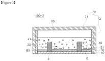
- a light source module 100-2 may have a structure in which the reflection unit 30 and a reflection pattern 31 are added to the first exemplary embodiment.
- the reflection unit 30 may be disposed between the flexible printed circuit board 10 and the resin layer 40, and the reflection pattern 31 may be further formed on the reflection unit 30.
- the reflection unit 30 and the reflection pattern 31 may function to improve the reflectance of light emitted from the light source 20.
- the reflection unit 30 may be composed of a material having high reflection efficiency.
- the reflection unit 30 reflects the light irradiated from the light source 20 onto one surface (for example, an upper surface) of the resin layer 40 so that the light is not leaked to another surface (for example, a lower surface) of the resin layer 40, thereby enabling light loss to be reduced.
- the reflection unit 30 may be composed in a single film form. To realize a characteristic for promoting the reflection and diffusion of light, the reflection unit 30 may be formed of the synthetic resin in which the white pigment is dispersedly contained.
- titanium oxide, aluminum oxide, zinc oxide, lead carbonate, barium sulfate, calcium carbonate and the like may be used as the white pigment.
- Polyethylene terephthalate, polyethylene naphthalate, acryl resin, poly carbonate, polystyrene, polyolefin, cellulose acetate, weather resistant vinyl chloride and the like may be used as the synthetic resin.
- the present invention is not limited to this.
- the reflection unit 30 may have a spacing part in an inner part thereof. The more detailed contents will be described in the description of FIG. 4 and FIG. 5 .
- the reflection pattern 31 may be disposed on a surface of the reflection unit 30 and may function to scatter and disperse incident light.
- the reflection pattern may be formed by printing the surface of the reflection unit with a reflection ink including any one of TiO 2 , CaCO 3 , BaSO 4 , Al 2 O 3 , Silicon, and PS (Polystyrene). However, it is not limited to this.
- a structure of the reflection pattern 31 may be a plurality of protruding patterns and may be regular or irregular.
- the reflection pattern 31 may be formed in a prism shape, a lenticular shape, a lens shape or a combined shape thereof.
- the shape is not limited to this.
- a cross section shape of the reflection pattern 31 may be composed in various shapes such as a polygonal shape of a triangular shape, a quadrangular shape and the like, a semicircular shape, a sinusoidal shape and the like.
- the shape thereof may be composed in a polygonal shape (e.g. a hexagonal shape), a circular shape, an elliptical shape or a semicircular shape.
- FIG. 16 shows one embodiment of the reflection pattern illustrated in FIG. 3 .
- the reflection pattern 31 may have different diameters from each other depending on a separation distance with the light source 20.
- a diameter of the reflection pattern 31 may be larger. Specifically, the diameter may be large in the order of a first reflection pattern 31-1, a second reflection pattern 31-2, a third reflection pattern 31-3 and a fourth reflection pattern 31-4.
- the present embodiment is not limited to this.
- the reflection pattern 31 of the present embodiment of the invention may be formed in various configurations such a configuration in which a density is changed depending on a distance with the light source, and a configuration in which a size and a density are all changed depending on a distance with the light source.
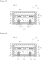
- FIG. 4 illustrates some embodiments of the reflection unit 30 and a separation member 37 which composes the reflection unit 30.
- the reflection unit 30 formed on the flexible printed circuit board has a spacing part 36 in an inner part thereof.
- the spacing part 36 functions to maximize brightness by increasing reflection efficiency of the light emitted from the light source.
- the reflection unit 30 may include a first reflection sheet 33 which is closely bonded onto the surface of the flexible printed circuit board (reference numeral 10 of FIG. 3 ), and a second reflection sheet 35 made of a transparent material and spaced apart from the first reflection film 33 to form the spacing part 36.
- the first and second reflection sheets 33, 35 are laminated on the flexible printed circuit board (reference numeral 10 of FIG. 3 ) and pass through a hole formed on the reflection unit 30 so that the light source (reference numeral 20 of FIG. 2 ) protrudes to the outside.
- the spacing part 36 may be formed by integrally compressing the first and second reflection sheets 33, 35 without using a separate member such as an adhesive agent. Furthermore, as illustrated in the drawing, the spacing part 36, in which air is received through the separation member 37 such as an adhesive member, may be implemented between the first reflection film 33 and the second reflection film 35.
- the first reflection sheet 33 may be formed using a reflection material which reflects light, for example, a film in which a metal layer such as Ag is formed on a base member.
- the first reflection sheet 33 may be implemented using the synthetic resin, in which a white pigment is dispersedly contained, such as white PET (polyethylen terephthalate) in order to implement a characteristic for promoting the reflection and dispersion of the light.
- white PET polyethylen terephthalate
- titanium oxide, aluminum oxide, zinc oxide, lead carbonate, barium sulfate, calcium carbonate and the like may be used as the white pigment.
- Polyethylene terephthalate, polyethylene naphthalate, acryl resin, poly carbonate, polystyrene, polyolefin, cellulose acetate, weather resistant vinyl chloride and the like may be used as the synthetic resin.
- the present embodiment is not limited to this.
- the second reflection sheet 35 may be implemented by a film made of a transparent material such as PET so that light emitted from the light source (reference numeral 20 of FIG. 3 ) is transmitted to the surface of the first reflection film 33 and the transmitted light is again reflected.
- the reflection pattern 31 may be further formed on the second reflection sheet 33 so that brightness can be improved by more promoting the dispersion of light.
- the reflection pattern 31 is an element which functions to scatter and disperse the incident light.
- the reflection pattern 31 may be formed by printing a surface of the second reflection sheet 3 5 with a reflective ink including any one of TiO 2 , CaCO 3 , BaSO 4 , Al 2 O 3 , Silicon, and PS (Polystyrene).
- a reflective ink including any one of TiO 2 , CaCO 3 , BaSO 4 , Al 2 O 3 , Silicon, and PS (Polystyrene).
- the present embodiment is not limited to this.
- FIG. 4 illustrates an exemplary embodiment of the separation member which composes the aforesaid reflection unit 30 stated in (a) of FIG. 4 .
- the separation member 37 according to the present invention may implement the spacing part 36 by performing only a general separation function such as a spacer member for simply separating the first reflection sheet 33 from the second reflection sheet 35 or a spacer member having an adhesive property. More preferably, in order to improve adhesive efficiency at the same time as improving disposition efficiency of the spacing part, when the separation member is implemented, a patterning structure illustrated in (b) of FIG. 4 may be uniformly and randomly formed.
- the separation member 37 illustrated in (b) of FIG. 4 may be implemented in a two-dimensional or three-dimensional structure in which a plurality of unit separation members 37a having a pore space part in an inner part is disposed, and a first separation part 37b is implemented in a structure in which an inner side of the unit separation member 37a is empty.
- a cross-section of the unit separation member 37a may be implemented in various shapes such as a polygonal shape, a circular shape and the like.
- the plurality of unit separation members 37a is irregularly disposed, so except for the first separation part 37b of the inner part of the unit separation members 37a, a second separation part 37 c, which is composed of a vacant space among the unit separation members 37a, may be further formed.
- the improvement of brightness as well as the improvement of light reflectance may be maximized.
- the brightness can be increased, and thanks to a pattern design of the separation member (the spacer) which forms the spacing part, the control of light and reflection efficiency can be maximized.
- FIG. 5 illustrates detailed one exemplary embodiment of the reflection unit stated in FIG. 4 .
- the reflection unit 30 includes the first reflection sheet 33 which is closely bonded onto the surface of the flexible printed circuit board, and the second reflection sheet 35 which is disposed to be opposite to the first reflection film 33.
- the film of the transparent material such as PET and the like may be applied to the second reflection sheet 35.
- the separation member 37 for separating the first reflection sheet 33 from the second reflection sheet 35 is provided by patterning an adhesive material, thereby enabling the spacing part to be formed.
- the first reflection sheet 33 has a film 331 onto which a metal reflection layer 38 is bonded by an adhesive agent (i.e. a primer).
- the film 331 may be also implemented in a structure which is laminated on a release film 335 by the adhesive material 333 (i.e. PSA).
- PSA adhesive material
- the first reflection sheet 33 of the present embodiment of the invention may be also implemented using white PET, which is the same as previously described in the description of FIG. 4 .
- FIG. 6 shows a third exemplary embodiment 100-3 of the light source module illustrated in FIG. 1 .
- the same reference numerals as those of FIG. 2 represent the same elements, and the contents overlapping with those stated earlier are omitted or are briefly stated.
- the light source module 100-3 may have a structure in which an optical pattern layer 50 is added to the first exemplary embodiment.
- the optical pattern layer 50 is disposed on the resin layer 40 and transmits the light emitted from one surface (for example, the upper surface) of the resin layer 40.
- the optical pattern layer 50 may be composed of a single optical sheet.
- the optical pattern layer 50 may be formed using a material having excellent light transmittance, for example, PET (Polyethylene Telephthalate).
- the first separated space 80 as stated in the description of FIG. 2 may be formed between the upper surface 71 of the diffusion plate 70, and the optical sheet. Thanks to the existence of the first separated space 80, the uniformity of light supplied to the diffusion plate 70 can be improved. Consequently, the uniformity of light diffused and emitted through the diffusion plate 70 can be improved, which is the same as previously described in the description of FIG. 2 .
- FIG. 6 and the optical pattern layer having other structures will be stated in the description of FIG. 8 to FIG. 10 .
- FIG. 7 shows a fourth exemplary embodiment 100-4 of the light source module illustrated in FIG. 1 .
- the same reference numerals as those of FIG. 2 represent the same elements, and the contents overlapping with those stated earlier are omitted or are briefly stated.
- the fourth exemplary embodiment may have a structure in which a heat dissipation member 110 is further included in the first exemplary embodiment.
- the heat dissipation member 110 is disposed on a lower surface of the flexible printed circuit board 10 and functions to emit the heat generated from the light source 20 to the outside. That is, the heat dissipation member 110 can improve efficiency for emitting the light generated from the light source 20, which is a heat source, to the outside.
- the heat dissipation member 110 may be disposed on one portion of the lower surface of the flexible printed circuit board 10.
- the heat dissipation member 110 may include a plurality of heat dissipation layers (e.g. 110-1, 110-2) which is spaced apart from each other.
- at least a part of the heat dissipation layers 110-1,110-2 may overlap with the light source 20 in a vertical direction.
- the vertical direction may be a direction which is toward the resin layer 40 from the flexible printed circuit board 10.
- the heat dissipation member 110 may be a material having high heat conductivity such as Al, an Al alloy, Cu, or a Cu alloy. Alternately, the heat dissipation member 110 may be an MCPCB (Metal Core Printed Circuit Board). The heat dissipation member 110 may be bonded onto the lower surface of the flexible printed circuit board 10 by an acryl-based adhesive agent (not drawn).
- luminous intensity of the light emitting device may be reduced, and the wavelength shift of generated light may be generated.
- the wavelength shift and the reduction in luminous intensity may be severely generated.
- the light source module 100-4 may control an increase in temperature of the light source by providing the heat dissipation member 110 on the lower surface of the flexible printed circuit board 10 to efficiently emit the heat generated from the light source 20.
- the reduction in luminous intensity of the light source module 100-4 or the generation of the wavelength shift of the light source module 100-4 may be controlled.
- FIG. 7 illustrates a structure in which the heat dissipation member 110 is added to the light source module 100-1 of FIG. 2 .
- the heat dissipation member can be also added to the light source modules 100-2, 100-3 of FIG. 3 and FIG. 6 which are the second exemplary embodiment and the third exemplary embodiment.
- FIG. 8 shows a fifth exemplary embodiment 100-5 of the light source module illustrated in FIG. 1 .
- the light source module 100-5 which is the optical pattern layer 50 added to the fourth exemplary embodiment 100-4, may be composed in a structure in which the optical pattern layer 50 includes a first optical sheet 52, an adhesive layer 56, an optical pattern 60 and a second optical sheet 54.
- the first optical sheet 52 is disposed on the resin layer 40, and the second optical sheet is disposed on the first optical sheet 52.
- the first optical sheet 52 and the second optical sheet 54 may be formed using a material having excellent light transmittance.
- PET may be used as the material.
- a thickness of the first optical sheet 52 or the second optical sheet may be formed in the range of 12 to 300 ,um. However, the thickness is not limited to this. The thickness may be appropriately changed depending on the lighting device's spec.
- the adhesive layer 56 is disposed between the first optical sheet 52 and the second optical sheet 54 to bond the first optical sheet 52 to the second optical sheet 54.
- the optical pattern 60 may be disposed on at least one of an upper surface of the first optical sheet 52 or a lower surface of the second optical sheet 54.
- the optical pattern 60 may be bonded onto at least one of the upper surface of the first optical sheet 52 and the lower surface of the second optical sheet 54 by the adhesive layer 56. Meanwhile, one or more optical sheets (not drawn) may be further included in the second optical sheet 54.
- the optical pattern 60 may be a light shielding pattern for preventing the concentration of light emitted from the light source 20.
- the optical pattern 60 may be aligned in the light source 20 and may be formed in a type which is bonded to the first optical sheet and the second optical sheet by the adhesive layer 56 or may be formed by being directly printed on at least any one surface of the first optical sheet 52 and the second optical sheet 54.
- the first optical sheet 52 and the second optical sheet 54 may be formed using a material having excellent light transmittance.
- PET may be used as the material.
- the optical pattern 60 basically functions to prevent the concentration of the light emitted from the light source 20. That is, the optical pattern 60 as well as the aforesaid reflection pattern 31 may function to implement uniform surface light emission.
- the optical pattern 60 may be a light shielding pattern for partially shielding the light emitted from the light source 20 and may prevent a reduction in optical characteristic or a yellowish phenomenon which is generated due to the excessively strong strength of light.
- the optical pattern 60 may prevent the concentration of light to an area which is adjacent to the light source 20 and may function to disperse the light.
- the optical pattern 60 may be formed by performing a printing process for the upper surface of the first optical sheet 52 or the lower surface of the second optical sheet 54 using the light shielding ink.
- the optical pattern 60 may adjust a light shielding degree or a light diffusion degree by adjusting at least one of a density and a size of the optical pattern so that the optical pattern 60 does not function to completely shield the light, but functions to partially shield and diffuse the light.
- a density of the optical pattern may be adjusted to get lower.
- the present embodiment is not limited to this.
- the optical pattern 60 may be implemented in an overlapping print structure of a composite pattern.
- the overlapping print structure means a structure in which one pattern is formed, and another pattern is printed on an upper part thereof.
- the optical pattern 60 may include a diffusion pattern and a light shielding pattern, and may be have a structure in which the diffusion pattern and the light shielding pattern overlap with each other.
- the diffusion pattern may be formed on a lower surface of a polymer film (e.g. the second optical sheet 54) in a light emitting direction using a light shielding ink including one or more materials selected from the group consisting of TiO 2 , CaCO 3 , BaSO 4 , Al 2 O 3 , Silicon, and PS (polystyrene).
- the light shielding pattern may be formed on the surface of the polymer film using a light shielding ink including Al or a mixture of Al and TiO 2 .
- the diffusion pattern is formed by white-printing it on the surface of the polymer film, the light shielding pattern is formed thereon.
- the diffusion pattern may be formed in a double structure.
- a formation design of this pattern may be variously modified in consideration of the efficiency and strength of light, and a light shielding rate.
- the optical pattern 60 may have a triple structure including the first diffusion pattern, the second diffusion pattern, and the light shielding pattern disposed therebetween.
- the optical pattern 60 may be implemented using the aforesaid materials.
- the first diffusion pattern may include TiO 2 having excellent refractive index
- the second diffusion pattern may include CaCO 3 and TiO 2 having excellent light stability and color sense
- the light shielding pattern may include Al having an excellent concealing property. Thanks to the optical pattern having the triple structure, the present exemplary embodiment can secure the efficiency and uniformity of light.
- CaCO 3 may function to reduce a yellowish phenomenon. Through this function, CaCO 3 may function to finally implement white light, thereby enabling light having more stable efficiency to be implemented.
- inorganic materials having a large particle size such as and a similar structure to BaSO 4 , Al 2 O 3 , silicon may be utilized as a diffusion material used in the diffusion pattern.
- the adhesive layer 56 may surround a periphery part of the optical pattern 60 and may fix the optical pattern 60 to at least any one of the first optical sheet 52 and the second optical sheet 54.
- a heat curing PSA, a heat curing adhesive agent or a UV curing PSA type material may be used in the adhesive layer 56.
- the present invention is not limited to this.
- FIG. 9 shows a sixth exemplary embodiment 100-6 of the light source module illustrated in FIG. 1 .
- the light source module 100-6 may have a structure in which a second separated space 81 is added to the fifth exemplary embodiment. That is, the optical pattern layer 50 in the sixth exemplary embodiment 100-6 may include the first optical sheet 52, the adhesive layer 56, the second optical sheet 54, the optical pattern, and the second separated space 81 formed between the first optical sheet 52 and the second optical sheet 54.
- the second separated space 81 may be formed in the adhesive layer 56.
- the adhesive layer 56 may form a separated space (i.e. the second separated space 81) around the optical pattern 60.
- the adhesive layer 56 may be implemented in a structure in which the first optical sheet 52 and the second optical sheet 54 are bonded to each other.
- the adhesive layer 56 may be composed in a structure in which the second separated space 81 is located in the periphery part of the optical pattern 60. Alternately, the adhesive layer 56 may be composed in a structure in which the adhesive layer 56 surrounds the periphery part of the optical pattern 60, and the second separated space 81 is located in a remaining part except for the periphery part.
- the adhesive structure of the first optical sheet 52 and the second optical sheet 54 may also implement a function for fixing the printed optical pattern 60. Since the second separated space 81 and the adhesive layer 56 have different refractive indexes from each other, the second separated space 81 may improve the diffusion and dispersion of light, which moves to a direction of the second optical sheet 56 from the first optical sheet 52. Due to this, a more uniform surface light source can be implemented.
- FIG. 10 conceptually illustrates the configuration of the optical pattern layer (reference numeral 50 of FIG. 9 ) illustrated in FIG. 9 .
- the adhesive layer 56 is formed in a structure which surrounds around the optical pattern 60 which is printed as a specific pattern on the first optical sheet stated in the description of FIG. 9 , and the second optical sheet is bonded thereto, so a regular separated space is formed.
- This separated space forms the second separated space 81 having a closed structure in which an air layer is formed.
- the shape of a plane of the second separated space 81 formed by the adhesive layer 56 may be composed in a circular shape as illustrated in the drawing.
- the shape may be implemented in various shapes such as an elliptical shape, a rectangular shape, a quadrate shape, a polygonal shape and the like.
- FIG. 11 shows a seventh exemplary embodiment 100-7 of the light source module illustrated in FIG. 1 .
- the light source module 100-7 may have a structure in which via holes 212, 214 for improving heat dissipation are provided in the flexible printed circuit board 10 of the first exemplary embodiment.
- the via holes 212,214 may pass through the flexible printed circuit board 110 and may expose a part of the light source 20 or a part of the resin layer 40.
- the via holes 212,214 may include a first via hole 212 to which the part of the light source 20 is exposed, and a second via hole 214 to which a part of the lower surface of the resin layer 40 is exposed.
- the heat generated from the light source which is a heat source may be directly emitted through the first via hole 212 to the outside.
- the heat transmitted from the light source 20 to the resin layer 40 may be directly emitted through the second via hole 214 to the outside.
- the sixth exemplary embodiment may improve the heat dissipation efficiency because the heat generated from the light source 20 is emitted through the via holes 212, 214 to the outside.
- the first via hole 212 and the second via hole 214 may have various shapes such as a polygonal shape, a circular shape, an elliptical shape and the like.
- FIG. 12 shows an eighth exemplary embodiment 100-8 of the light source module illustrated in FIG. 1 .
- the same reference numerals as those of FIG. 1 represent the same elements, and the contents overlapping with those stated earlier are omitted or are briefly stated.
- a heat dissipation member 310 of the light source module 100-8 may have a lower heat dissipation layer 310-1 which is disposed on the lower surface of the flexible printed circuit board 10, and a through part 310-1 in which a part of the lower heat dissipation layer 310-1 is in contact with the light source 20 by passing through the flexible printed circuit board 10.
- the through part 310-1 may be in contact with a first side surface part 714 of first lead frames 620, 620' of light emitting device packages 200-1, 200-2 which will be described later.
- the heat dissipation efficiency can be improved.
- heat dissipation member 310 can be also included in the aforesaid second and third exemplary embodiments even through this is not illustrated in the drawing.
- FIG. 13 shows a ninth exemplary embodiment 100-9 of the light source module illustrated in FIG. 1
- FIG. 14 shows a tenth exemplary embodiment 100-9 of the light source module illustrated in FIG. 1
- FIG. 15 shows an eleventh exemplary embodiment 100-9 of the light source module illustrated in FIG. 1 .
- the light source module illustrated in FIG. 13 to FIG. 15 may have a structure in which an additional element is further added to the reflection sheet 30, the second optical sheet 54 and the diffusion plate 70.
- embossments R1, R2, R3 may be formed on at least one surface or both surfaces of the reflection sheet 30, the second optical sheet 54 and the diffusion plate 70.
- the embossments R1, R2, R3 reflect and diffuse the incident light, thereby enabling the light emitted to the outside to form a geometrical pattern.
- the first embossment R1 may be formed on one surface (e.g. the upper surface) of the reflection sheet 30, the second embossment R2 may be formed on one surface (e.g. the upper surface) of the second optical sheet 54, and the third embossment R3 may be formed on one surface (e.g. the lower surface) of the diffusion plate 70.
- These embossments R1, R2, R3 may be formed in a structure in which a plurality of patterns is regularly or irregularly provided.
- the embossments may be composed in a prism shape, a lenticular shape, a concave lens shape, a convex lens shape or a combined shape thereof. However, their shape is not limited to this.
- each cross-sectional shape of the embossments R1, R2, R3 may be composed in various structures having various shapes such as a triangular shape, a quadrangular shape, a semi circular shape, a sinusoidal shape and the like. Furthermore, each pattern size and density may be changed depending on a distance with the light source 20.
- the embossments R1, R2, R3 may be formed by directly processing the reflection sheet 30, the second optical sheet 54 and the diffusion plate 70. This is not limited.
- the embossments R1, R2, R3 may be formed by a method of attaching a film in which regular patterns are formed, a method of directly attaching a lens (e.g. a prism lens and a lenticular lens) and all other methods which have been developed and commercialized or can be implemented depending on future technical development.
- a geometrical optical pattern may be easily implemented through a combination of the patterns of the first to third embossments R1, R2, R3.
- the embossments may be formed on one surface or both surfaces of the second optical sheet 54.
- the exemplary embodiments in which the embossment R1, R2 or R3 is formed are not limited to FIG. 13 to FIG. 15 .
- the embossment R1, R2 or R3 may be also formed on at least one surface or both surfaces of the reflection sheet 30, the first optical sheet 52, the second optical sheet 54 and the diffusion plate 70 included in the other exemplary embodiments.
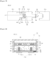
- FIG. 17 shows a plane view of a twelfth exemplary embodiment 100-12 of the light source module illustrated in FIG. 1
- FIG. 18 shows a cross-sectional view taken along AA' of the light source module 100-12 illustrated in FIG. 17
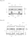
- FIG. 19 shows a cross-sectional view taken along BB' of the light source module 100-12 illustrated in FIG. 17
- FIG. 20 shows a cross-sectional view taken along CC' of the light source module 100-12 illustrated in FIG. 17 .
- the light source module 100-12 may include a plurality of sub-light source modules 101-1 to 101-n (n represents natural numbers greater than 1, n>1).
- the plurality of sub-light source modules 101-1 to 101-n may be separated from or connected to each other.
- the plurality of sub-light source modules 101-1 to 101-n may be electrically connected to each other.
- the formation of the diffusion 70 and the light reflection member 90 may be performed by combining each sub-light source module 101-1 to 101-n with each other, and thereafter connecting the diffusion plate 70 formed in an inner side of the side wall 73 to the entire combination structure using the light reflection member 90.
- Each sub-light source module 101-1 to 101-n includes at least one connector (e.g. 510, 520, 530) which may be connected to the outside.
- the first sub-light source module 101-1 may include the first connector 510 including at least one terminal (e.g. S1, S2).
- the second sub-light source 101-2 may include the first connector 520 and the second connector 530 which are connected to the outside, respectively.
- the first connector 520 may include at least one terminal (e.g. P1, P2)
- the second connector 530 may include at least one terminal (e.g. Q1, Q2).
- the first terminal (S1, P1, Q1) may be a positive (+) terminal
- the second terminal (S2, P2, Q2) may be a negative (-) terminal.
- FIG. 19 illustrates that each connector (e.g. 510, 520, 530) includes two terminals. However, the number of terminals is not limited to this.
- FIG. 18 through FIG. 20 illustrate a structure in which the connector 510, 520 or 530 is added to the sixth exemplary embodiment 100-6.
- the respective sub-light source modules 101-1 to 101-n may have a structure in which the connector 510, 520 or 530 and a connection fixing unit (e.g. 410-1, 420-1, 420-2) are added to the light source module according to any one of the aforesaid exemplary embodiments.
- the respective sub-light source modules 101-1 to 101-n include: the flexible printed circuit board 10; the light source 20; the reflection sheet 30; the reflection pattern 31; the resin layer 40; the first optical sheet 52; the second optical sheet 54; the adhesive layer 56; the optical pattern 60; the heat dissipation member 110; at least one connector 510, 520 or 530; and at least one connection fixing unit 410, 420.
- the same reference numerals as those of FIG. 1 represent the same elements, and the contents overlapping with those stated earlier are omitted or are briefly stated.
- the respective sub-light source modules 101-1 to 101-n of the twelfth exemplary embodiment may have a difference with respect to each size or each number of light sources, but except for the connector and the connection fixing unit, the structure thereof may be identical to each structure of other exemplary embodiments.
- the first sub-light source module 101-1 may be electrically connected to the light source 20 and may include a first connector 510 provided to the flexible printed circuit board 10 so as to be electrically connected to the outside.
- the first connector 510 may be implemented in a type which is patterned on the flexible printed circuit board 10.
- the second sub-light source module 101-2 may include the first connector 520 and the second connector 530 which are electrically connected to the light source 20.
- the first connector 520 may be provided at one side of the flexible printed circuit board 10 to be electrically connected to the first connector 510 of the outside (e.g. the first sub-light source module 101-1).
- the second connector 530 may be provided at another side of the flexible printed circuit board 10 to be electrically connected to the connector (not drawn) of another outside (e.g. the third sub-light source module 101-3).
- Connection fixing units e.g. 410-1, 420-1, 420-2 are connected to other sub-light source modules of the outside and function to fix two connected sub-light source modules to each other.
- the connection fixing units 410-1, 420-1, 420-2 may be a protrusion part (p) having a type in which a part of the side surface of the resin layer 40 protrudes, or a groove part having a type in which a part of the side surface of the resin layer 40 is recessed.
- the first sub-light source module 101-1 may include a first connection fixing unit 410-1 having a structure in which a part of the side surface of the resin layer 40 protrudes.
- the second sub-light source module 101-2 may include the first connection fixing unit 420-1 having a structure in which a part of the side surface of the resin layer 40 is recessed.
- the first connection fixing unit 410-1 of the first sub-light source module 101-1 and the first connection fixing unit 420-1 of the second sub-light source module 101-2 may be connected and fixed to each other.
- connection fixing unit e.g. 410-1, 420-1
- the connection fixing unit is implemented in a part of the resin layer 40.
- the exemplary embodiment is not limited to this.
- a separate connection fixing unit may be provided, and the connection fixing unit may be changed in connectable other types.
- the sub-light source modules 101-1 to 101-n may have a shape in which a fixed part protrudes.
- the shape is not limited to this.
- the sub-light source modules may be implemented in various shapes.
- the shape thereof when looking down the sub-light source modules 101-1 to 101-n (n represents natural numbers greater than 1>1) from the above, the shape thereof may be a circular shape, an elliptical shape a polygonal shape, and a shape in which a part protrudes in a side direction.
- one end of the first sub-light source module 101-1 may include a protrusion part 540 in a center thereof.
- the first connector 510 may be provided to the flexible printed circuit board 10 corresponding to the protrusion part 540.
- the first connection fixing unit 410-1 may be provided to the resin layer 40 of a remaining part of the one end of the first sub-light source module 101-1 except for the protrusion part 540.
- one end of the second sub-light source module 101-2 may have a groove part 545 in a center thereof, the second connector 520 may be provided in the flexible printed circuit board 10 corresponding to the groove part 545, and the first connection fixing unit 420-1 may be provided to the resin layer 40 of the remaining part of one end of the second sub-light source 101-2 except for the groove part 545.
- another end of the second sub-light source module 101-2 may include a protrusion part 560 in its center, the third connector 530 may be provided in the flexible printed circuit board 10 corresponding to the protrusion part 560, and the second connection fixing unit 420-2 may be provided to the resin layer 40 of the remaining part of one end of the second sub-light source 101-2 except for the protrusion part 560.
- Each of the sub-light source modules 101-1 to 101-n may be an independent light source, and a shape thereof may be variously changed. Since two or more sub-light source modules may be assembled to each other by the connection fixing unit, and thus may be used as the independent light source, the present exemplary embodiment can improve a degree of freedom in product design. Also, in the present exemplary embodiment, in a case where some parts of the assembled sub-light source modules are damaged or broken, only the damaged sub-light source module may be exchanged and used.
- the aforesaid light source module may be used in a display device, an indicating device and a lighting system which require a surface light source.
- the light source module according to some exemplary embodiment may be easily mounted in a place (e.g. a ceiling or a bottom having a bend) in which illumination is required, but installation of the illumination cannot be easily performed because a part for mounting the illumination has a bend.
- the lighting system may include a lamp or a streetlamp.
- the lamp may be a head lamp for a vehicle.
- the lamp is not limited to this.
- FIG. 21 shows a head lamp for a vehicle 900-1 according to an exemplary embodiment
- FIG. 43 shows a general head lamp for a vehicle, which a point light source.
- the head lamp for the vehicle 900-1 includes a light source module 910 and a light housing 920.
- the light source module 910 may be shown in the aforesaid exemplary embodiments 100-1 to 100-12.
- the light housing 920 may receive the light source module 910 and may be composed of a transparent material.
- the light housing 920 for a vehicle may include a bend depending on a portion and design of the vehicle which is mounted. Meanwhile, as described above, the diffusion plate itself may perform a function of the light housing 920 for the vehicle. In addition to the diffusion plate, the separate light housing 920 for the vehicle may be provided, which is the same as previously described.
- the light source module 910 itself has flexibility because it uses the flexible printed circuit board 10 and the resin layer 40, so the light source module 910 may be easily mounted to the light housing for the vehicle 920 having the bend.
- the head lamp for the vehicle 900-1 may prevent the generation of wavelength shift and the reduction of luminous intensity. Also, as described above, the separate light reflection member is formed on the side surface of the resin layer, so light loss can be reduced and the improvement of brightness compared to same electric power can be implemented.
- the general head lamp for the vehicle as illustrated in FIG. 43 is a point light source, when it emits light, a spot 930 may be partially generated from a light emitting surface.
- the head lamp for the vehicle 900-1 according the present exemplary embodiment is a surface light source, the spot cannot be generated and uniform brightness and roughness can be implemented all over the light emitting surface.
Landscapes
- Engineering & Computer Science (AREA)
- General Engineering & Computer Science (AREA)
- Physics & Mathematics (AREA)
- Optics & Photonics (AREA)
- General Physics & Mathematics (AREA)
- Microelectronics & Electronic Packaging (AREA)
- Mechanical Engineering (AREA)
- Planar Illumination Modules (AREA)
- Arrangement Of Elements, Cooling, Sealing, Or The Like Of Lighting Devices (AREA)
- Non-Portable Lighting Devices Or Systems Thereof (AREA)
- Led Device Packages (AREA)
Description
- This application claims priority to
Korean Patent Application Nos. 10-2012-0065259 10-2012-0065260 10-2012-0065264, filed on June 18, 2012 - Embodiments of the present invention relate to the technology field of a lighting device.
- An LED (Light Emitted Diode) device is a device which converts an electrical signal to infrared rays or light using a composition semiconductor property. Unlike a florescent lamp, since the LED device does not use harmful substances such as mercury and the like, it has a low possibility to cause environmental pollution and a long life span compared to a conventional light source. Also, it is advantageous that the LED device spends low electricity compared to the conventional light source and has excellent visibility and low brilliantness due to a high color temperature.
- Accordingly, a current lighting device has been developed from a structure, in which a traditional light source such as a conventional incandescent lamp or a florescent lamp is used, to a structure, in which the aforesaid LED device is used as a light source. In particular, by using a light guide plate as disclosed in
Korean Laid-Open Patent Publication No. 10-2012-0009209 - The aforesaid lighting device is composed in a structure in which a flat light guide plate is disposed on a substrate, and a plurality of side view type LEDs is disposed on a side of the light guide plate in an array shape. Here, the light guide plate is a kind of plastic molding lens which functions to uniformly supply light emitted from the LEDs. Accordingly, in the conventional lighting device, the light guide plate is used as an essential component. However, due to a thickness of the light guide plate itself, there is a limitation to make the thickness of an entire product thin. Furthermore, as a material of the light guide plate is not flexible, it is disadvantageous that it would be difficult to apply the light guide plate to a part in which a bend is formed, and thus a product plan and design cannot be easily changed.
- Also, as the light is partially emitted to the side of the light guide plate, light loss is generated. Thus, it is problematic that light efficiency is reduced. Furthermore, as a temperature of the LEDs increases at the time of light emission, it is also problematic that the LEDs' characteristics (e.g. luminous intensity and wavelength transition) are changed.
-
Korean Laid-Open Patent Publication No. 10-2012-0009209 US 2010/220474 A1 discloses a light emitting device including: a plurality of barriers provided above a metal circuit board; a plurality of light emitting devices placed in a space between the barriers; and a lens unit provided at an upper side of the barrier.US 2009/016067 A1 discloses an optical plate including at least one transparent plate unit, each optical plate comprising a first surface, a second surface, a plurality of enclosing V-shaped protrusions, a diffusion layer and a lamp-receiving portion. - Embodiments of the present invention have been made keeping in mind the above problems occurring in the related art. An aspect of the present invention provides a lighting device that can get thinner in thickness, improve a degree of freedom in product design and heat dissipation efficiency, and control a wavelength shift and a reduction in luminous intensity.
- Another aspect of embodiments of the present invention provides a lighting device which can improve brightness by minimizing light loss.
- Still another aspect of embodiments of the present invention provides a lighting device which can maximize the improvement of brightness without the addition of a light source by forming a reflection unit having a spacing part on a printed circuit board to improve light reflectance.
- Still further another aspect of embodiments of the present invention provides a lighting device which can prevent the generation of a hot spot while improving the uniformity of light by forming an optical pattern layer having an optical pattern in the lighting device.
- These objects are achieved by providing a lighting device according to the invention, said lighting device having the features of
independent claim 1. Preferred embodiments are defined in the dependent claims. - According to the present invention, there is provided a lighting device comprising: a printed circuit board; a plurality of light sources disposed on the printed circuit board; a resin layer disposed on the reflection unit so that the light sources are embedded; a reflection unit formed between the printed circuit board and the resin layer; a light reflection member(90) disposed on both side surfaces of the resin layer(40); and a diffusion plate(70) having an upper surface(71) disposed over the light sources and a side wall(73) which is integrally formed with the upper surface(71) and formed to extend in a lower side direction, and which is adhered onto the light reflection member, wherein the upper surface(71) of the diffusion plate(70) is spaced apart from the resin layer, wherein the reflection unit(30) comprises a reflection sheet(33) disposed on the printed circuit board(10), a transparent sheet(35) disposed on the reflection sheet(33), and a separation member(37) disposed between the reflection sheet(33) and the transparent sheet(35), and characterized in that the separation member(37) comprises a plurality of unit separation members(37a), and a cross sectional shape of at least one of the unit separation members(37a) comprises a polygonal shape .
- The advantageous effect according to the embodiments of the present invention is that the light reflection module is provided so that the light loss generated from the side surface of the resin layer can be minimized, thereby enabling brightness and roughness of the lighting device to be improved.
- Also, still another advantageous effect according to the embodiments of the present invention is that the light guide plate is removed and the resin layer is used to guide light so that the number of light emitting device packages can be reduced, and a total thickness of the lighting device can get thinner.
- Also, still further advantageous effect according to the embodiments of the present invention is that the resin layer is formed of high heat resistant resin so that, in spite of the heat generated from the light source package, stable brightness can be implemented and the lighting device having high reliability can be provided.
- Moreover, still further advantageous effect according to the embodiments of the present invention is that the lighting device is formed using the flexible printed circuit board and the resin layer so that flexibility can be secured, thereby enabling a degree of freedom in product design to be improved.
- Furthermore, still further advantageous effect according to the embodiments of the present invention is that the diffusion plate itself surrounds a side surface of the light source module so that the diffusion plate itself can perform the function of a housing, and thus as a separate structure is not used, manufacturing process efficiency and, durability and reliability of the product itself can be improved. Also, according to the embodiments of the present invention, heat dissipation efficiency can be improved and a wavelength shift and a reduction in illumination intensity can be controlled.
- Also, still further advantageous effect according to the embodiments of the present invention is that the light reflection member is provided so that the light loss generated from the side surface of the resin layer can be minimized, thereby enabling brightness and roughness of the lighting device to be improved.
- Also, still further advantageous effect according to the embodiments of the present invention is that the reflection unit having the spacing part is provided on the surface of the printed circuit board so that the improvement of light reflectance as well as the improvement of brightness can be maximized. Furthermore, although the thickness of the lighting device and the number of the light source are not increased, the brightness can be improved, and thanks to a pattern design of the separation member (i.e. a spacer) which forms the spacing part, the control of light and reflection efficiency can be maximized.
- Also, still further advantageous effect according to the embodiments of the present invention is that the optical pattern layer is formed in the light source module so that the concentration of light and the generation of a hot spot can be prevented, and the uniformity of light supplied to the diffusion plate can be improved.
- The accompanying drawings are included to provide a further understanding of the present invention, and are incorporated in and constitute a part of this specification. The drawings illustrate exemplary embodiments of the present invention and, together with the description, serve to explain principles of the present invention. In the drawings:
-
FIG. 1 shows a lighting device according to an exemplary embodiment of the present invention; -
FIG. 2 andFIG. 3 show first and second exemplary embodiments of a light source module illustrated inFIG. 1 ; -
FIG. 4 andFIG. 5 illustrate an exemplary embodiments of a separation member which composes a reflection unit stated inFIG. 3 ; -
FIG. 6 through FIG. 9 show third to sixth exemplary embodiments of the light source module illustrated inFIG. 1 ; -
FIG. 10 illustrates an exemplary embodiment of an optical pattern layer according to the present invention; -
FIG. 11 through FIG. 15 show seventh to eleventh exemplary embodiments of the light source module illustrated inFIG. 1 ; -
FIG. 16 shows an exemplary embodiment of a reflection pattern illustrated inFIG. 3 ; -
FIG. 17 shows a plane view of a twelfth exemplary embodiment of the light source module illustrated inFIG. 1 ; -
FIG. 18 shows a cross-sectional view taken along AA' of the light source module illustrated inFIG. 17 ; -
FIG. 19 shows a cross-sectional view taken along BB' of the light source module illustrated inFIG. 17 ; -
FIG. 20 shows a cross-sectional view taken along CC' of the light source module illustrated inFIG. 17 ; -
FIG. 21 shows a head lamp for a vehicle according to an exemplary embodiment of the present invention; - Embodiments according to the present invention will now be described more fully hereinafter with reference to the accompanying drawings so that those having ordinary skill in the art can easily embody. This invention may, however, be embodied in different forms and should not be construed as limited to the exemplary embodiments set forth herein. It is to be understood that the form of the present invention shown and described herein is to be taken as a preferred embodiment of the present invention and that various changes and modifications may be made in the invention without departing from the spirit and scope thereof. Also, in the following description, it is to be noted that, when the functions of conventional elements and the detailed description of elements related with the present invention may make the gist of the present invention unclear, a detailed description of those elements will be omitted. Reference will now be made in greater detail to a preferred embodiment of the invention, an example of which is illustrated in the accompanying drawings. Wherever possible, the same reference numerals will be used throughout the drawings and the description to refer to the same or like parts.
- Embodiments of the present invention relate to a lighting device. The gist thereof is to provide a structure of the lighting device which is configured such that a light guide plate is removed, a resin layer is replaced with the light guide plate, and a light reflection member is formed on a side surface of the resin layer so that brightness and roughness can be improved, and a total thickness of the lighting device can be innovatively reduced. Furthermore, as the diffusion plate is used as a support of the light reflection member by processing the diffusion plate, an integral property, durability and reliability of the product can be secured, and flexibility of the lighting device itself can be also secured.
- Moreover, the lighting device according to the embodiments of the present invention may be applied to various lamp devices such as a lamp for a vehicle, a lighting device for home use and an industrial lighting device for which illumination is required. For example, when the lighting device is applied to the lamp for the vehicle, it can be also applied to a headlight, indoor illumination for the vehicle, a door scarf, a back light and the like. In addition to this, the lighting device of the present invention can be applied to the field of a backlight unit applied to a liquid crystal display device. Except for this, the light device can be applied to all fields relating to illumination, which has been currently developed and commercialized or can be realized depending on future technical development.
- Hereinafter, the light source module means that remaining elements except for a diffusion plate and a light reflection member are referred to as one.
-
FIG. 1 illustrates alighting device 1 according to an embodiment of the present invention. Referring toFIG. 1 , thelighting device 1 includes alight source module 100 which is a surface light source. Also, thelighting device 1 may further include a housing150 for receiving thelight source module 100. - The
light source module 100 includes at least one light source for generating light. The light source may be composed of a light emitting device package including a light emitting chip. Thelight source module 100 may implement a surface light source by diffusing and dispersing the light generated from the light source, which is a point light source, and may have be bent due to its flexibility. - The
housing 150 may protect thelight source module 100 from an impact and may be composed of a material (for example, acryl) to which the light irradiated from thelight source module 100 can be transmitted. Also, since thehousing 150 may include a bending part in view of a design and thelight source module 100 may have flexibility, the light source module can be easily received in the bendinghousing 150. Of course, since thehousing 150 itself has constant flexibility, a total assembly structure of thelighting device 1 itself can also have constant flexibility. -
FIG. 2 shows a first exemplary embodiment (100-1) of the light source module illustrated inFIG. 1 , and more specifically, a cross-sectional view taken along AB of the light device illustrated inFIG. 1 . Referring toFIG. 2 , the light source module (100-1) includes: a printedcircuit board 10; alight source 20; and aresin layer 40 for performing the function of a light guide plate. Alight reflection member 90 is formed on at least one of one side surface and another side surface of theresin layer 40, and adiffusion plate 70 is formed on the aforesaid light source module 100-1. - The printed
circuit board 10 may be a flexible printed circuit board using an insulating substrate having flexibility. For example, the flexible printedcircuit board 10 may include a base member (for example, reference numeral 5) and a circuit pattern (for example, reference numerals 6 and 7) disposed on at least one surface of the base member (for example, reference numeral 5). A material of the base member (for example, reference numeral 5) may be a film having flexibility and an insulating property, for example, polyimide or epoxy (for example, FR-4). - More specifically, the flexible printed
circuit board 10 may include an insulating film 5 (for example, polyimide or FR-4), a first copper foil pattern 6, a secondcopper foil pattern 7, and a viacontact 8. The first copper foil pattern 6 is formed on one surface (for example, an upper surface) of the insulatingfilm 5, and the secondcopper foil pattern 7 is formed on another surface (for example, a lower surface) of the insulatingfilm 5. The first copper foil pattern 6 and the secondcopper foil pattern 7 may be connected through the viacontact 8 formed to pass through the insulatingfilm 5. - Hereinafter, a case in which the printed
circuit board 10 is composed of the aforesaid flexible printed circuit board will be stated as an example. However, this is only an example. In addition to this, various types of boards may be used as the printedcircuit board 10 of the present invention. - The
light source 20 is disposed in one or more number on the flexible printedcircuit board 10, thereby emitting light. For example, thelight source 20 may be a side view type light emitting device package which is disposed so that the emitted light moves to adirection 3 being toward a side surface of theresin layer 40. At this time, the light emitting chip mounted to the light emitting device package may be a vertical type light emitting chip. For example, the light emitting chip may be a red light-emitting chip illustrated in FIG. 43. However, the present embodiment is not limited to this. - The
resin layer 40 may be disposed in the printedcircuit board 10 and an upper part of thelight source 20 so that thelight source 20 is embedded, and may diffuse and induce the light emitted from thelight source 20 to a side direction of theresin layer 40 in a direction being toward one surface (for example, an upper surface) of theresin layer 40. - The
resin layer 40 may be composed of a resin material which can diffuse the light. A refractive index thereof may range from 1.4 to 1.8. However, the refractive index is not limited to this. - For example, the
resin layer 40 may be composed of an ultraviolet curing resin having a high heat resistant property and including a oligomer. At this time, a content of the oligomer may range from 40 to 50 wt.%. Also, urethane acrylate may be used as the ultraviolet curing resin. However, it is not limited to this. In addition to this, at least one material of epoxy acrylate, polyester acrylate, polyether acrylate, polybutadiene acrylate, and silicon acrylate may be used. - In particular, when the urethane acrylate is used as the oligomer, different physical properties from each other may be simultaneously implemented by using a mixture of two types of urethane acrylate.
- For example, when isocyanate is used during synthesizing the urethane acrylate, physical properties (i.e. a yellowing property, a weather resistant property, and a chemically resistant property) of the urethane acrylate are determined by the isocyanate. At this time, when any one kind of urethane acrylate is implemented as urethane acrylate type-isocyanate, it is implemented that NCO % of PDI (isophorone diisocyanate) or IPDI (isophorone diisocyanate) becomes 37% (hereinafter referred to as 'a first oligomer'). Furthermore, when another one kind of urethane acrylate is implemented as the urethane acrylate type-isocyanate, it is implemented that NCO % of PDI (isophorone diisocyanate) or IPDI (isophorone diisocyanate) becomes 30 to 50% or 25 to 35% (hereinafter referred to as 'a second oligomer'). Thus, the oligomer according to the present exemplary embodiment may be formed. According to this, as NCO% is adjusted, the first oligomer and the second oligomer having different physical properties from each other may be obtained, and the oligomer which forms the
resin layer 40 may be implemented by the first and second oligomers. A weight ratio of the first oligomer in the oligomer may be implemented in the range of 15 to 20, and a weight ratio of the second oligomer in the oligomer may be implemented in the range of 25 to 35. - Meanwhile, the
resin layer 40 may further include any one of a monomer and a photo initiator. At this time, a content of the monomer may be formed in 65 to 90 parts by weight. More specifically, the monomer may be formed of a mixture including 35 to 45 parts by weight of IBOA (isobornyl acrylate), 10 to 15 pars by weight of 2-HEMA (2-hydroxyethyl methacrylate), and 15 to 20 parts by weight of 2-HBA (2-hydroxybutyl acrylate). Moreover, the photoinitiator (for example, 1-hydroxycyclohexyl phenyl-ketone, diphenyl) and diphenyl(2,4,6-trimethylbenzoyl phosphine oxide and the like) may be formed in 0.5 to 1 parts by weight. - Also, the
resin layer 40 may be composed of a heat curing resin having a high heat resistant property. Specifically, theresin layer 40 may be composed of a heat curing resin including at least one of a polyester polyol resin, an acryl polyol resin, a hydrocarbon-based solvent or/and an ester-based solvent. The heat curing resin may further include a hest curing agent to improve coating strength. - In the case of the polyester polyol resin, a content of the polyester polyol resin may range from 9 to 30% based on a total weight of the heat curing resin. Also, in the case of the acryl polyol resin, a content of the acryl polyol resin may range from 20 to 40% based on the total weight of the heat curing resin.
- In the case of the hydrocarbon-based solvent or the ester-based solvent, a content thereof may range from 30 to 70% based on the total weight of the heat curing resin. In the case of the heat curing agent, a content thereof may range from 1 to 10% based on the total weight of the heat curing resin. When the
resin layer 40 is formed of the aforesaid materials, the heat resistant property of the resin layer is reinforced. Thus, even though the resin layer is used in the lighting device from which the heat of a high temperature is emitted, a reduction in brightness due to heat can be minimized, thereby enabling the lighting device having high reliability to be provided. - Also, according to the present embodiment of present invention, as the aforesaid materials are used to implement a surface light source, a thickness of the
resin layer 40 can be innovatively reduced. Thus, a whole product can be implemented to get thinner in thickness. Furthermore, according to the present invention, since the lighting device is formed using the flexible printed circuit board and the resin layer made of a flexible material, it can be easily applied to a bending surface. Thus, it is advantageous that a degree of freedom in design can be improved, and the lighting device can be applied to other flexible display devices. - The
resin layer 40 may include adiffusion material 41 having a hollow (or a pore space) in an inner part thereof. Thediffusion material 41 may have a shape which is mixed or diffused with resin which composes theresin layer 40, and may function to improve light reflection and diffusion properties. - For example, as light emitted from the
light source 20 to an inner part of theresin layer 40 is reflected and transmitted by the hollow of thediffusion material 41, the light may be diffused and concentrated in theresin layer 40, and the diffused and concentrated light may be emitted to one surface (e.g. an upper part surface) of theresin layer 40. At this time, since reflectance and a diffusion rate of the light are improved due to thediffusion material 41, an amount and uniformity of the emission light supplied to the upper surface of theresin layer 40 can be improved, thereby enabling brightness of the light source module 100-1 to be improved. - A content of the
diffusion material 41 may be appropriately adjusted to obtain a desired light diffusion effect. Specifically, the content may be adjusted in the range of 0.01 to 0.3% based on the total weight of theresin layer 40. However, the content is not limited to this. Thediffusion material 41 may be composed of any one selected from the group consisting of silicon, silica, glass bubble, PMMA, urethane, Zn, Zr, Al2O3, and acryl. A particle diameter of thediffusion material 41 may be 1 µm to 20 µm. However, the particle diameter is not limited to this. - The
light reflection member 90 is formed on at least one of one side surface and another side surface of theresin layer 40. Thelight reflection member 90 guides so that the light irradiated from thelight emitting device 20 is emitted to the upper part of the resin layer, and performs as a guide function for preventing light from being emitted through the side surface of theresin layer 40 to the outside. Thereflection member 90 may be composed of a material having excellent light reflectance such as a white resist. In addition to this, thelight reflection member 90 may be composed of a synthetic resin in which a white pigment is dispersed, or a synthetic resin in which metal particles having an excellent light reflection property are dispersed. At this time, titanium oxide, aluminum oxide, zinc oxide, lead carbonate, barium sulfate, calcium carbonate and the like may be used as the white pigment. When the metal particles are included, Ag powders having excellent reflectance may be included. Also, a separate fluorescent brightening agent may be additionally included. That is, thelight reflection member 90 of the present embodiment of the invention may be formed using all materials having excellent light reflectance, which has developed or can be implemented depending on future technical development. Meanwhile, thelight reflection member 90 may be directly molded and connected to the side surface of theresin layer 40 or may be bonded thereto by a separate adhesive material (or an adhesive tape). - Moreover, the
light reflection member 90 may be directly molded and connected to an inner side of aside wall 73 of thediffusion plate 70, may be bonded thereto by a separate adhesive material or may be connected to thediffusion plate 70 by being directly printed to the inner side of theside wall 73. - Also, the drawing illustrates that the
light reflection member 90 is formed all over the inner side of theside wall 73 of the diffusion plate 79. However, this is only one example. Thelight reflection member 90 may be formed only on the side surface of theresin layer 40 or may be formed on both the side surface of theresin layer 40 and the side surface of the printedcircuit board 10. That is, if the range includes the side surface of theresin layer 40, the formation range of thelight reflection member 90 is not limited. - Thus, as the
light reflection member 90 is formed on the side surface of theresin layer 40, the leakage of light to the side surface of theresin layer 40 can be prevented, so light loss can be reduced, light efficiency can be improved, and brightness and roughness of the lighting device can be improved under a same electricity condition. - The
diffusion plate 70 may be disposed in an upper part of the light source module 100-1, more specifically, on theresin layer 40, and may function to uniformly diffuse the light emitted through theresin layer 40 throughout a whole surface. A thickness of thediffusion plate 70 may be basically formed in the range of 0.5 to 5mm. However, the thickness is not limited to this. The thickness may be appropriately designed and changed depending on the lighting device's spec. In particular, as illustrated inFIG. 2 , thediffusion plate 70 of the present invention is formed in a structure having anupper surface 71 and theside wall 73 integrally formed with theupper surface 71. At this time, theside wall 73 surrounds a side surface of the light source module 100-1. Thediffusion plate 70 may be generally formed of an acryl resin. However, the material is not limited to this. In addition to this, thediffusion plate 70 may be formed of a high penetrating plastic material capable of performing a light diffusion function such as poly styrene (PS), polymethyl methacrylate (PMMA), cyclic olefin copolymer (COC), polyethylene terephthalate (PET), and resin. - A first separated
space 80 may be present between an upper surface of thediffusion plate 70 and the resin layer. Thanks to the existence of the first separated space, a difference in refractive index with theresin layer 40 may be generated, thereby enabling the uniformity of light supplied to thediffusion plate 70 to be improved. Consequently, the uniformity of light diffused and emitted through thediffusion plate 70 may be improved. At this time, to minimize a deviation in light which transmits theresin layer 40, a thickness of the first separatedspace 80 may be formed in the range which is more than 0 but is less than 30mm. However, the thickness is not limited to this. This can be changed in design as needed. - The
side wall 73 of thediffusion plate 70 surrounds the side surface of the light source module 100-1. As described above, theside wall 73 may perform the function of a support for supporting thelight reflection member 90 and the function of a housing for protecting the light source module 100-1. That is, thediffusion plate 70 according to the present embodiment of the invention may perform the function of thehousing 150 illustrated inFIG. 1 as needed. Accordingly, the diffusion plate itself surrounds the side surface of the light source module 100-1, so the diffusion plate itself may perform the function of the housing. Thus, as a separate structure is not used, it is advantageous that manufacturing process efficiency and durability and reliability of the product itself can be improved. - Referring to
FIG. 3 , a light source module 100-2 may have a structure in which thereflection unit 30 and areflection pattern 31 are added to the first exemplary embodiment. - The
reflection unit 30 may be disposed between the flexible printedcircuit board 10 and theresin layer 40, and thereflection pattern 31 may be further formed on thereflection unit 30. Thereflection unit 30 and thereflection pattern 31 may function to improve the reflectance of light emitted from thelight source 20. - The
reflection unit 30 may be composed of a material having high reflection efficiency. Thereflection unit 30 reflects the light irradiated from thelight source 20 onto one surface (for example, an upper surface) of theresin layer 40 so that the light is not leaked to another surface (for example, a lower surface) of theresin layer 40, thereby enabling light loss to be reduced. Thereflection unit 30 may be composed in a single film form. To realize a characteristic for promoting the reflection and diffusion of light, thereflection unit 30 may be formed of the synthetic resin in which the white pigment is dispersedly contained. - For example, titanium oxide, aluminum oxide, zinc oxide, lead carbonate, barium sulfate, calcium carbonate and the like may be used as the white pigment. Polyethylene terephthalate, polyethylene naphthalate, acryl resin, poly carbonate, polystyrene, polyolefin, cellulose acetate, weather resistant vinyl chloride and the like may be used as the synthetic resin. However, the present invention is not limited to this.
- Also, the
reflection unit 30 may have a spacing part in an inner part thereof. The more detailed contents will be described in the description ofFIG. 4 andFIG. 5 . - The
reflection pattern 31 may be disposed on a surface of thereflection unit 30 and may function to scatter and disperse incident light. The reflection pattern may be formed by printing the surface of the reflection unit with a reflection ink including any one of TiO2, CaCO3, BaSO4, Al2O3, Silicon, and PS (Polystyrene). However, it is not limited to this. - Also, a structure of the
reflection pattern 31 may be a plurality of protruding patterns and may be regular or irregular. To improve the scattering effect of light, thereflection pattern 31 may be formed in a prism shape, a lenticular shape, a lens shape or a combined shape thereof. However, the shape is not limited to this. Also, inFIG. 3 , a cross section shape of thereflection pattern 31 may be composed in various shapes such as a polygonal shape of a triangular shape, a quadrangular shape and the like, a semicircular shape, a sinusoidal shape and the like. Also, when looking down thereflection pattern 31 from the above, the shape thereof may be composed in a polygonal shape (e.g. a hexagonal shape), a circular shape, an elliptical shape or a semicircular shape. -
FIG. 16 shows one embodiment of the reflection pattern illustrated inFIG. 3 . Referring toFIG. 16 , thereflection pattern 31 may have different diameters from each other depending on a separation distance with thelight source 20. - For example, as the
reflection pattern 31 becomes gradually adjacent to thelight source 20, a diameter of thereflection pattern 31 may be larger. Specifically, the diameter may be large in the order of a first reflection pattern 31-1, a second reflection pattern 31-2, a third reflection pattern 31-3 and a fourth reflection pattern 31-4. However, the present embodiment is not limited to this. In addition to this, thereflection pattern 31 of the present embodiment of the invention may be formed in various configurations such a configuration in which a density is changed depending on a distance with the light source, and a configuration in which a size and a density are all changed depending on a distance with the light source. - In the lighting device of the embodiment of the present invention stated in the description of the
FIG. 3 ,FIG. 4 illustrates some embodiments of thereflection unit 30 and aseparation member 37 which composes thereflection unit 30. - Referring to
FIG. 3 to (a) ofFIG. 4 , thereflection unit 30 formed on the flexible printed circuit board has aspacing part 36 in an inner part thereof. Thespacing part 36 functions to maximize brightness by increasing reflection efficiency of the light emitted from the light source. - In particular, the
reflection unit 30 may include afirst reflection sheet 33 which is closely bonded onto the surface of the flexible printed circuit board (reference numeral 10 ofFIG. 3 ), and asecond reflection sheet 35 made of a transparent material and spaced apart from thefirst reflection film 33 to form thespacing part 36. The first andsecond reflection sheets reference numeral 10 ofFIG. 3 ) and pass through a hole formed on thereflection unit 30 so that the light source (reference numeral 20 ofFIG. 2 ) protrudes to the outside. - The
spacing part 36 may be formed by integrally compressing the first andsecond reflection sheets part 36, in which air is received through theseparation member 37 such as an adhesive member, may be implemented between thefirst reflection film 33 and thesecond reflection film 35. - The
first reflection sheet 33 may be formed using a reflection material which reflects light, for example, a film in which a metal layer such as Ag is formed on a base member. Alternately, thefirst reflection sheet 33 may be implemented using the synthetic resin, in which a white pigment is dispersedly contained, such as white PET (polyethylen terephthalate) in order to implement a characteristic for promoting the reflection and dispersion of the light. At this time, titanium oxide, aluminum oxide, zinc oxide, lead carbonate, barium sulfate, calcium carbonate and the like may be used as the white pigment. Polyethylene terephthalate, polyethylene naphthalate, acryl resin, poly carbonate, polystyrene, polyolefin, cellulose acetate, weather resistant vinyl chloride and the like may be used as the synthetic resin. However, the present embodiment is not limited to this. - The
second reflection sheet 35 may be implemented by a film made of a transparent material such as PET so that light emitted from the light source (reference numeral 20 ofFIG. 3 ) is transmitted to the surface of thefirst reflection film 33 and the transmitted light is again reflected. - Meanwhile, the
reflection pattern 31 may be further formed on thesecond reflection sheet 33 so that brightness can be improved by more promoting the dispersion of light. Thereflection pattern 31 is an element which functions to scatter and disperse the incident light. Thereflection pattern 31 may be formed by printing a surface of thesecond reflection sheet 3 5 with a reflective ink including any one of TiO2, CaCO3, BaSO4, Al2O3, Silicon, and PS (Polystyrene). However, the present embodiment is not limited to this. - (b) of
FIG. 4 illustrates an exemplary embodiment of the separation member which composes theaforesaid reflection unit 30 stated in (a) ofFIG. 4 . Theseparation member 37 according to the present invention may implement thespacing part 36 by performing only a general separation function such as a spacer member for simply separating thefirst reflection sheet 33 from thesecond reflection sheet 35 or a spacer member having an adhesive property. More preferably, in order to improve adhesive efficiency at the same time as improving disposition efficiency of the spacing part, when the separation member is implemented, a patterning structure illustrated in (b) ofFIG. 4 may be uniformly and randomly formed. - The
separation member 37 illustrated in (b) ofFIG. 4 may be implemented in a two-dimensional or three-dimensional structure in which a plurality ofunit separation members 37a having a pore space part in an inner part is disposed, and afirst separation part 37b is implemented in a structure in which an inner side of theunit separation member 37a is empty. At this time, a cross-section of theunit separation member 37a may be implemented in various shapes such as a polygonal shape, a circular shape and the like. In particular, as illustrated, in addition to a structure in which the plurality ofunit separation members 37a is disposed to be closely adhered to each other, the plurality ofunit separation members 37a is irregularly disposed, so except for thefirst separation part 37b of the inner part of theunit separation members 37a, asecond separation part 37 c, which is composed of a vacant space among theunit separation members 37a, may be further formed. Thus, in the lighting device of the present embodiment of the invention including theaforesaid reflection unit 30, as thereflection unit 30 having the spacing part is provided, the improvement of brightness as well as the improvement of light reflectance may be maximized. Also, although a thickness of the lighting device or the number of light sources is not increased, the brightness can be increased, and thanks to a pattern design of the separation member (the spacer) which forms the spacing part, the control of light and reflection efficiency can be maximized. -
FIG. 5 illustrates detailed one exemplary embodiment of the reflection unit stated inFIG. 4 . - As aforesaid, the
reflection unit 30 according to the present embodiment of the invention includes thefirst reflection sheet 33 which is closely bonded onto the surface of the flexible printed circuit board, and thesecond reflection sheet 35 which is disposed to be opposite to thefirst reflection film 33. - In particular, the film of the transparent material such as PET and the like may be applied to the
second reflection sheet 35. Theseparation member 37 for separating thefirst reflection sheet 33 from thesecond reflection sheet 35 is provided by patterning an adhesive material, thereby enabling the spacing part to be formed. - In particular, to maximize reflection efficiency, the
first reflection sheet 33 has afilm 331 onto which ametal reflection layer 38 is bonded by an adhesive agent (i.e. a primer). Thefilm 331 may be also implemented in a structure which is laminated on arelease film 335 by the adhesive material 333 (i.e. PSA). However, this is only one example. In addition to this, thefirst reflection sheet 33 of the present embodiment of the invention may be also implemented using white PET, which is the same as previously described in the description ofFIG. 4 . -
FIG. 6 shows a third exemplary embodiment 100-3 of the light source module illustrated inFIG. 1 . The same reference numerals as those ofFIG. 2 represent the same elements, and the contents overlapping with those stated earlier are omitted or are briefly stated. - Referring to
FIG. 6 , the light source module 100-3 may have a structure in which anoptical pattern layer 50 is added to the first exemplary embodiment. - The
optical pattern layer 50 is disposed on theresin layer 40 and transmits the light emitted from one surface (for example, the upper surface) of theresin layer 40. Theoptical pattern layer 50 may be composed of a single optical sheet. In this case, theoptical pattern layer 50 may be formed using a material having excellent light transmittance, for example, PET (Polyethylene Telephthalate). - Meanwhile, when the
optical pattern layer 50 is formed of the single optical sheet, the first separatedspace 80 as stated in the description ofFIG. 2 may be formed between theupper surface 71 of thediffusion plate 70, and the optical sheet. Thanks to the existence of the first separatedspace 80, the uniformity of light supplied to thediffusion plate 70 can be improved. Consequently, the uniformity of light diffused and emitted through thediffusion plate 70 can be improved, which is the same as previously described in the description ofFIG. 2 . -
FIG. 6 and the optical pattern layer having other structures will be stated in the description ofFIG. 8 to FIG. 10 . -
FIG. 7 shows a fourth exemplary embodiment 100-4 of the light source module illustrated inFIG. 1 . The same reference numerals as those ofFIG. 2 represent the same elements, and the contents overlapping with those stated earlier are omitted or are briefly stated. - Referring to
FIG. 7 , to improve heat dissipation efficiency, the fourth exemplary embodiment may have a structure in which aheat dissipation member 110 is further included in the first exemplary embodiment. - The
heat dissipation member 110 is disposed on a lower surface of the flexible printedcircuit board 10 and functions to emit the heat generated from thelight source 20 to the outside. That is, theheat dissipation member 110 can improve efficiency for emitting the light generated from thelight source 20, which is a heat source, to the outside. - For example, the
heat dissipation member 110 may be disposed on one portion of the lower surface of the flexible printedcircuit board 10. Theheat dissipation member 110 may include a plurality of heat dissipation layers (e.g. 110-1, 110-2) which is spaced apart from each other. In order to improve a heat dissipation effect, at least a part of the heat dissipation layers 110-1,110-2 may overlap with thelight source 20 in a vertical direction. Here, the vertical direction may be a direction which is toward theresin layer 40 from the flexible printedcircuit board 10. - The
heat dissipation member 110 may be a material having high heat conductivity such as Al, an Al alloy, Cu, or a Cu alloy. Alternately, theheat dissipation member 110 may be an MCPCB (Metal Core Printed Circuit Board). Theheat dissipation member 110 may be bonded onto the lower surface of the flexible printedcircuit board 10 by an acryl-based adhesive agent (not drawn). - In general, when the temperature of a light emitting device increases due to heat generated from the light emitting device, luminous intensity of the light emitting device may be reduced, and the wavelength shift of generated light may be generated. In particular, when the light emitting device is a red light emitting diode, the wavelength shift and the reduction in luminous intensity may be severely generated.
- However, the light source module 100-4 may control an increase in temperature of the light source by providing the
heat dissipation member 110 on the lower surface of the flexible printedcircuit board 10 to efficiently emit the heat generated from thelight source 20. Thus, the reduction in luminous intensity of the light source module 100-4 or the generation of the wavelength shift of the light source module 100-4 may be controlled. -
FIG. 7 illustrates a structure in which theheat dissipation member 110 is added to the light source module 100-1 ofFIG. 2 . However, it would also be obvious to those having ordinary skill in the art that the heat dissipation member can be also added to the light source modules 100-2, 100-3 ofFIG. 3 andFIG. 6 which are the second exemplary embodiment and the third exemplary embodiment. -
FIG. 8 shows a fifth exemplary embodiment 100-5 of the light source module illustrated inFIG. 1 . - Referring to
FIG. 8 , the light source module 100-5, which is theoptical pattern layer 50 added to the fourth exemplary embodiment 100-4, may be composed in a structure in which theoptical pattern layer 50 includes a firstoptical sheet 52, anadhesive layer 56, anoptical pattern 60 and a secondoptical sheet 54. - The first
optical sheet 52 is disposed on theresin layer 40, and the second optical sheet is disposed on the firstoptical sheet 52. The firstoptical sheet 52 and the secondoptical sheet 54 may be formed using a material having excellent light transmittance. For example, PET may be used as the material. At this time, a thickness of the firstoptical sheet 52 or the second optical sheet may be formed in the range of 12 to 300 ,um. However, the thickness is not limited to this. The thickness may be appropriately changed depending on the lighting device's spec. - The
adhesive layer 56 is disposed between the firstoptical sheet 52 and the secondoptical sheet 54 to bond the firstoptical sheet 52 to the secondoptical sheet 54. - The
optical pattern 60 may be disposed on at least one of an upper surface of the firstoptical sheet 52 or a lower surface of the secondoptical sheet 54. Theoptical pattern 60 may be bonded onto at least one of the upper surface of the firstoptical sheet 52 and the lower surface of the secondoptical sheet 54 by theadhesive layer 56. Meanwhile, one or more optical sheets (not drawn) may be further included in the secondoptical sheet 54. Theoptical pattern 60 may be a light shielding pattern for preventing the concentration of light emitted from thelight source 20. Theoptical pattern 60 may be aligned in thelight source 20 and may be formed in a type which is bonded to the first optical sheet and the second optical sheet by theadhesive layer 56 or may be formed by being directly printed on at least any one surface of the firstoptical sheet 52 and the secondoptical sheet 54. - The first
optical sheet 52 and the secondoptical sheet 54 may be formed using a material having excellent light transmittance. For example, PET may be used as the material. Theoptical pattern 60 basically functions to prevent the concentration of the light emitted from thelight source 20. That is, theoptical pattern 60 as well as theaforesaid reflection pattern 31 may function to implement uniform surface light emission. - The
optical pattern 60 may be a light shielding pattern for partially shielding the light emitted from thelight source 20 and may prevent a reduction in optical characteristic or a yellowish phenomenon which is generated due to the excessively strong strength of light. For example, theoptical pattern 60 may prevent the concentration of light to an area which is adjacent to thelight source 20 and may function to disperse the light. - The
optical pattern 60 may be formed by performing a printing process for the upper surface of the firstoptical sheet 52 or the lower surface of the secondoptical sheet 54 using the light shielding ink. Theoptical pattern 60 may adjust a light shielding degree or a light diffusion degree by adjusting at least one of a density and a size of the optical pattern so that theoptical pattern 60 does not function to completely shield the light, but functions to partially shield and diffuse the light. As one example, to improve light efficiency, as a distance between theoptical pattern 60 and thelight source 20 increases, a density of the optical pattern may be adjusted to get lower. However, the present embodiment is not limited to this. - Specifically, the
optical pattern 60 may be implemented in an overlapping print structure of a composite pattern. The overlapping print structure means a structure in which one pattern is formed, and another pattern is printed on an upper part thereof. - As one example, the
optical pattern 60 may include a diffusion pattern and a light shielding pattern, and may be have a structure in which the diffusion pattern and the light shielding pattern overlap with each other. For example, the diffusion pattern may be formed on a lower surface of a polymer film (e.g. the second optical sheet 54) in a light emitting direction using a light shielding ink including one or more materials selected from the group consisting of TiO2, CaCO3, BaSO4, Al2O3, Silicon, and PS (polystyrene). Furthermore, the light shielding pattern may be formed on the surface of the polymer film using a light shielding ink including Al or a mixture of Al and TiO2. - That is, after the diffusion pattern is formed by white-printing it on the surface of the polymer film, the light shielding pattern is formed thereon. In the reverse order of the above one, the diffusion pattern may be formed in a double structure. Of course, it would be obvious that a formation design of this pattern may be variously modified in consideration of the efficiency and strength of light, and a light shielding rate.
- Alternately, in another exemplary embodiment, the
optical pattern 60 may have a triple structure including the first diffusion pattern, the second diffusion pattern, and the light shielding pattern disposed therebetween. In this triple structure, theoptical pattern 60 may be implemented using the aforesaid materials. As one example, the first diffusion pattern may include TiO2 having excellent refractive index, the second diffusion pattern may include CaCO3 and TiO2 having excellent light stability and color sense, and the light shielding pattern may include Al having an excellent concealing property. Thanks to the optical pattern having the triple structure, the present exemplary embodiment can secure the efficiency and uniformity of light. In particular, CaCO3 may function to reduce a yellowish phenomenon. Through this function, CaCO3 may function to finally implement white light, thereby enabling light having more stable efficiency to be implemented. In addition of CaCO3, inorganic materials having a large particle size such as and a similar structure to BaSO4, Al2O3, silicon may be utilized as a diffusion material used in the diffusion pattern. - The
adhesive layer 56 may surround a periphery part of theoptical pattern 60 and may fix theoptical pattern 60 to at least any one of the firstoptical sheet 52 and the secondoptical sheet 54. At this time, a heat curing PSA, a heat curing adhesive agent or a UV curing PSA type material may be used in theadhesive layer 56. However, the present invention is not limited to this. -
FIG. 9 shows a sixth exemplary embodiment 100-6 of the light source module illustrated inFIG. 1 . - Referring to
FIG. 9 , the light source module 100-6 may have a structure in which a second separatedspace 81 is added to the fifth exemplary embodiment. That is, theoptical pattern layer 50 in the sixth exemplary embodiment 100-6 may include the firstoptical sheet 52, theadhesive layer 56, the secondoptical sheet 54, the optical pattern, and the second separatedspace 81 formed between the firstoptical sheet 52 and the secondoptical sheet 54. - For example, the second separated
space 81 may be formed in theadhesive layer 56. Theadhesive layer 56 may form a separated space (i.e. the second separated space 81) around theoptical pattern 60. Furthermore, by applying an adhesive material to remaining parts, theadhesive layer 56 may be implemented in a structure in which the firstoptical sheet 52 and the secondoptical sheet 54 are bonded to each other. - The
adhesive layer 56 may be composed in a structure in which the second separatedspace 81 is located in the periphery part of theoptical pattern 60. Alternately, theadhesive layer 56 may be composed in a structure in which theadhesive layer 56 surrounds the periphery part of theoptical pattern 60, and the second separatedspace 81 is located in a remaining part except for the periphery part. The adhesive structure of the firstoptical sheet 52 and the secondoptical sheet 54 may also implement a function for fixing the printedoptical pattern 60. Since the second separatedspace 81 and theadhesive layer 56 have different refractive indexes from each other, the second separatedspace 81 may improve the diffusion and dispersion of light, which moves to a direction of the secondoptical sheet 56 from the firstoptical sheet 52. Due to this, a more uniform surface light source can be implemented. -
FIG. 10 conceptually illustrates the configuration of the optical pattern layer (reference numeral 50 ofFIG. 9 ) illustrated inFIG. 9 . Theadhesive layer 56 is formed in a structure which surrounds around theoptical pattern 60 which is printed as a specific pattern on the first optical sheet stated in the description ofFIG. 9 , and the second optical sheet is bonded thereto, so a regular separated space is formed. This separated space forms the second separatedspace 81 having a closed structure in which an air layer is formed. At this time, the shape of a plane of the second separatedspace 81 formed by theadhesive layer 56 may be composed in a circular shape as illustrated in the drawing. In addition to this, the shape may be implemented in various shapes such as an elliptical shape, a rectangular shape, a quadrate shape, a polygonal shape and the like. -
FIG. 11 shows a seventh exemplary embodiment 100-7 of the light source module illustrated inFIG. 1 . Referring toFIG. 11 , the light source module 100-7 may have a structure in which viaholes circuit board 10 of the first exemplary embodiment. - The via holes 212,214 may pass through the flexible printed
circuit board 110 and may expose a part of thelight source 20 or a part of theresin layer 40. For example, the via holes 212,214 may include a first viahole 212 to which the part of thelight source 20 is exposed, and a second viahole 214 to which a part of the lower surface of theresin layer 40 is exposed. - The heat generated from the light source which is a heat source may be directly emitted through the first via
hole 212 to the outside. The heat transmitted from thelight source 20 to theresin layer 40 may be directly emitted through the second viahole 214 to the outside. The sixth exemplary embodiment may improve the heat dissipation efficiency because the heat generated from thelight source 20 is emitted through the via holes 212, 214 to the outside. The first viahole 212 and the second viahole 214 may have various shapes such as a polygonal shape, a circular shape, an elliptical shape and the like. - Also, it would be obvious to those having ordinary skill in the art that the via holes 212, 214 can be also included in the second and third exemplary embodiments, even though this is not illustrated in the drawing.
-
FIG. 12 shows an eighth exemplary embodiment 100-8 of the light source module illustrated inFIG. 1 . The same reference numerals as those ofFIG. 1 represent the same elements, and the contents overlapping with those stated earlier are omitted or are briefly stated. - Referring to
FIG. 12 , unlike theheat dissipation member 110 of the fourth exemplary embodiment 100-4, aheat dissipation member 310 of the light source module 100-8 may have a lower heat dissipation layer 310-1 which is disposed on the lower surface of the flexible printedcircuit board 10, and a through part 310-1 in which a part of the lower heat dissipation layer 310-1 is in contact with thelight source 20 by passing through the flexible printedcircuit board 10. - For example, the through part 310-1 may be in contact with a first side surface part 714 of first lead frames 620, 620' of light emitting device packages 200-1, 200-2 which will be described later.
- According to the eighth exemplary embodiment, thanks to the through part 310-1, since the heat generated from the
light source 20 is directly transmitted to theheat dissipation member 310 and the transmitted light is emitted to the outside, the heat dissipation efficiency can be improved. - Also, it would be obvious to those having ordinary skill in the art that the
heat dissipation member 310 can be also included in the aforesaid second and third exemplary embodiments even through this is not illustrated in the drawing. -
FIG. 13 shows a ninth exemplary embodiment 100-9 of the light source module illustrated inFIG. 1 ,FIG. 14 shows a tenth exemplary embodiment 100-9 of the light source module illustrated inFIG. 1 , andFIG. 15 shows an eleventh exemplary embodiment 100-9 of the light source module illustrated inFIG. 1 . - The light source module illustrated in
FIG. 13 to FIG. 15 may have a structure in which an additional element is further added to thereflection sheet 30, the secondoptical sheet 54 and thediffusion plate 70. - More specifically, embossments R1, R2, R3 may be formed on at least one surface or both surfaces of the
reflection sheet 30, the secondoptical sheet 54 and thediffusion plate 70. The embossments R1, R2, R3 reflect and diffuse the incident light, thereby enabling the light emitted to the outside to form a geometrical pattern. - For example, the first embossment R1 may be formed on one surface (e.g. the upper surface) of the
reflection sheet 30, the second embossment R2 may be formed on one surface (e.g. the upper surface) of the secondoptical sheet 54, and the third embossment R3 may be formed on one surface (e.g. the lower surface) of thediffusion plate 70. These embossments R1, R2, R3 may be formed in a structure in which a plurality of patterns is regularly or irregularly provided. To improve a light reflection and diffusion effect, the embossments may be composed in a prism shape, a lenticular shape, a concave lens shape, a convex lens shape or a combined shape thereof. However, their shape is not limited to this. - Also, each cross-sectional shape of the embossments R1, R2, R3 may be composed in various structures having various shapes such as a triangular shape, a quadrangular shape, a semi circular shape, a sinusoidal shape and the like. Furthermore, each pattern size and density may be changed depending on a distance with the
light source 20. - The embossments R1, R2, R3 may be formed by directly processing the
reflection sheet 30, the secondoptical sheet 54 and thediffusion plate 70. This is not limited. The embossments R1, R2, R3 may be formed by a method of attaching a film in which regular patterns are formed, a method of directly attaching a lens (e.g. a prism lens and a lenticular lens) and all other methods which have been developed and commercialized or can be implemented depending on future technical development. - In the present exemplary embodiment, a geometrical optical pattern may be easily implemented through a combination of the patterns of the first to third embossments R1, R2, R3. In another exemplary embodiment, the embossments may be formed on one surface or both surfaces of the second
optical sheet 54. - However, the exemplary embodiments in which the embossment R1, R2 or R3 is formed are not limited to
FIG. 13 to FIG. 15 . To improve the light reflection and diffusion effect, the embossment R1, R2 or R3 may be also formed on at least one surface or both surfaces of thereflection sheet 30, the firstoptical sheet 52, the secondoptical sheet 54 and thediffusion plate 70 included in the other exemplary embodiments. -
FIG. 17 shows a plane view of a twelfth exemplary embodiment 100-12 of the light source module illustrated inFIG. 1 ,FIG. 18 shows a cross-sectional view taken along AA' of the light source module 100-12 illustrated inFIG. 17 ,FIG. 19 shows a cross-sectional view taken along BB' of the light source module 100-12 illustrated inFIG. 17 , andFIG. 20 shows a cross-sectional view taken along CC' of the light source module 100-12 illustrated inFIG. 17 . - Referring to
FIG. 17 to FIG. 20 , the light source module 100-12 may include a plurality of sub-light source modules 101-1 to 101-n (n represents natural numbers greater than 1, n>1). The plurality of sub-light source modules 101-1 to 101-n may be separated from or connected to each other. Also, the plurality of sub-light source modules 101-1 to 101-n may be electrically connected to each other. At this time, the formation of thediffusion 70 and thelight reflection member 90 may be performed by combining each sub-light source module 101-1 to 101-n with each other, and thereafter connecting thediffusion plate 70 formed in an inner side of theside wall 73 to the entire combination structure using thelight reflection member 90. - Each sub-light source module 101-1 to 101-n includes at least one connector (e.g. 510, 520, 530) which may be connected to the outside. For example the first sub-light source module 101-1 may include the
first connector 510 including at least one terminal (e.g. S1, S2). The second sub-light source 101-2 may include thefirst connector 520 and thesecond connector 530 which are connected to the outside, respectively. Thefirst connector 520 may include at least one terminal (e.g. P1, P2), and thesecond connector 530 may include at least one terminal (e.g. Q1, Q2). At this time, the first terminal (S1, P1, Q1) may be a positive (+) terminal, and the second terminal (S2, P2, Q2) may be a negative (-) terminal.FIG. 19 illustrates that each connector (e.g. 510, 520, 530) includes two terminals. However, the number of terminals is not limited to this. -
FIG. 18 through FIG. 20 illustrate a structure in which theconnector connector - Referring to
FIG. 18 andFIG. 19 , the respective sub-light source modules 101-1 to 101-n include: the flexible printedcircuit board 10; thelight source 20; thereflection sheet 30; thereflection pattern 31; theresin layer 40; the firstoptical sheet 52; the secondoptical sheet 54; theadhesive layer 56; theoptical pattern 60; theheat dissipation member 110; at least oneconnector FIG. 1 represent the same elements, and the contents overlapping with those stated earlier are omitted or are briefly stated. Comparing the present exemplary embodiment with other exemplary embodiments, the respective sub-light source modules 101-1 to 101-n of the twelfth exemplary embodiment may have a difference with respect to each size or each number of light sources, but except for the connector and the connection fixing unit, the structure thereof may be identical to each structure of other exemplary embodiments. - The first sub-light source module 101-1 may be electrically connected to the
light source 20 and may include afirst connector 510 provided to the flexible printedcircuit board 10 so as to be electrically connected to the outside. For example, thefirst connector 510 may be implemented in a type which is patterned on the flexible printedcircuit board 10. - Also, the second sub-light source module 101-2 may include the
first connector 520 and thesecond connector 530 which are electrically connected to thelight source 20. Thefirst connector 520 may be provided at one side of the flexible printedcircuit board 10 to be electrically connected to thefirst connector 510 of the outside (e.g. the first sub-light source module 101-1). Thesecond connector 530 may be provided at another side of the flexible printedcircuit board 10 to be electrically connected to the connector (not drawn) of another outside (e.g. the third sub-light source module 101-3). - Connection fixing units (e.g. 410-1, 420-1, 420-2) are connected to other sub-light source modules of the outside and function to fix two connected sub-light source modules to each other. The connection fixing units 410-1, 420-1, 420-2 may be a protrusion part (p) having a type in which a part of the side surface of the
resin layer 40 protrudes, or a groove part having a type in which a part of the side surface of theresin layer 40 is recessed. - Referring to
FIG. 20 , the first sub-light source module 101-1 may include a first connection fixing unit 410-1 having a structure in which a part of the side surface of theresin layer 40 protrudes. Also, the second sub-light source module 101-2 may include the first connection fixing unit 420-1 having a structure in which a part of the side surface of theresin layer 40 is recessed. - The first connection fixing unit 410-1 of the first sub-light source module 101-1 and the first connection fixing unit 420-1 of the second sub-light source module 101-2 may be connected and fixed to each other.
- The present exemplary embodiment illustrates that the connection fixing unit (e.g. 410-1, 420-1) is implemented in a part of the
resin layer 40. However, the exemplary embodiment is not limited to this. A separate connection fixing unit may be provided, and the connection fixing unit may be changed in connectable other types. - The sub-light source modules 101-1 to 101-n (n represents natural numbers greater than 1, n>1) may have a shape in which a fixed part protrudes. However, the shape is not limited to this. The sub-light source modules may be implemented in various shapes. For example, when looking down the sub-light source modules 101-1 to 101-n (n represents natural numbers greater than 1>1) from the above, the shape thereof may be a circular shape, an elliptical shape a polygonal shape, and a shape in which a part protrudes in a side direction.
- For example, one end of the first sub-light source module 101-1 may include a
protrusion part 540 in a center thereof. Thefirst connector 510 may be provided to the flexible printedcircuit board 10 corresponding to theprotrusion part 540. The first connection fixing unit 410-1 may be provided to theresin layer 40 of a remaining part of the one end of the first sub-light source module 101-1 except for theprotrusion part 540. - Also, one end of the second sub-light source module 101-2 may have a
groove part 545 in a center thereof, thesecond connector 520 may be provided in the flexible printedcircuit board 10 corresponding to thegroove part 545, and the first connection fixing unit 420-1 may be provided to theresin layer 40 of the remaining part of one end of the second sub-light source 101-2 except for thegroove part 545. Furthermore, another end of the second sub-light source module 101-2 may include aprotrusion part 560 in its center, thethird connector 530 may be provided in the flexible printedcircuit board 10 corresponding to theprotrusion part 560, and the second connection fixing unit 420-2 may be provided to theresin layer 40 of the remaining part of one end of the second sub-light source 101-2 except for theprotrusion part 560. - Each of the sub-light source modules 101-1 to 101-n may be an independent light source, and a shape thereof may be variously changed. Since two or more sub-light source modules may be assembled to each other by the connection fixing unit, and thus may be used as the independent light source, the present exemplary embodiment can improve a degree of freedom in product design. Also, in the present exemplary embodiment, in a case where some parts of the assembled sub-light source modules are damaged or broken, only the damaged sub-light source module may be exchanged and used.
- The aforesaid light source module may be used in a display device, an indicating device and a lighting system which require a surface light source. In particular, it is advantageous that the light source module according to some exemplary embodiment may be easily mounted in a place (e.g. a ceiling or a bottom having a bend) in which illumination is required, but installation of the illumination cannot be easily performed because a part for mounting the illumination has a bend. For example, the lighting system may include a lamp or a streetlamp. The lamp may be a head lamp for a vehicle. However, the lamp is not limited to this.
-
FIG. 21 shows a head lamp for a vehicle 900-1 according to an exemplary embodiment, and FIG. 43 shows a general head lamp for a vehicle, which a point light source. Referring toFIG. 21 , the head lamp for the vehicle 900-1 includes alight source module 910 and alight housing 920. - The
light source module 910 may be shown in the aforesaid exemplary embodiments 100-1 to 100-12. Thelight housing 920 may receive thelight source module 910 and may be composed of a transparent material. Thelight housing 920 for a vehicle may include a bend depending on a portion and design of the vehicle which is mounted. Meanwhile, as described above, the diffusion plate itself may perform a function of thelight housing 920 for the vehicle. In addition to the diffusion plate, the separatelight housing 920 for the vehicle may be provided, which is the same as previously described. Thelight source module 910 itself has flexibility because it uses the flexible printedcircuit board 10 and theresin layer 40, so thelight source module 910 may be easily mounted to the light housing for thevehicle 920 having the bend. Also, since the light source modules 100-1 to 100-12 has a structure in which heat dissipation efficiency is improved, the head lamp for the vehicle 900-1 according to the present exemplary embodiment may prevent the generation of wavelength shift and the reduction of luminous intensity. Also, as described above, the separate light reflection member is formed on the side surface of the resin layer, so light loss can be reduced and the improvement of brightness compared to same electric power can be implemented. - Since the general head lamp for the vehicle as illustrated in FIG. 43 is a point light source, when it emits light, a spot 930 may be partially generated from a light emitting surface. However, since the head lamp for the vehicle 900-1 according the present exemplary embodiment is a surface light source, the spot cannot be generated and uniform brightness and roughness can be implemented all over the light emitting surface.
Claims (9)
- A lighting device comprising:a printed circuit board(10);a plurality of light sources(20) disposed on the printed circuit board(10);a reflection unit disposed on the printed circuit board (10);a resin layer(40) disposed on the reflection unit(30) so that the light sources are embedded; andthe reflection unit(30) is formed between the printed circuit board(10) and the resin layer(40);a light reflection member(90) disposed on both side surfaces of the resin layer(40); anda diffusion plate(70) having an upper surface(71) disposed over the light sources and a side wall(73) which is integrally formed with the upper surface(71) and formed to extend in a lower side direction, and which is adhered onto the light reflection member,wherein the upper surface(71) of the diffusion plate(70) is spaced apart from the resin layer,wherein the reflection unit(30) comprises a reflection sheet(33) disposed on the printed circuit board(10), a transparent sheet(35) disposed on the reflection sheet(33), and a separation member(37) disposed between the reflection sheet(33) and the transparent sheet(35), andcharacterized in that the separation member(37) comprises a plurality of unit separation members(37a), and a cross sectional shape of at least one of the unit separation members(37a) comprises a polygonal shape.
- The lighting device of claim 1, wherein the separation member(37) further comprises a plurality of first separation part(37b),
wherein each of the plurality of the first separation parts(37b) is disposed in each of the plurality of the unit separation members(37a). - The lighting device of claim 2, wherein a cross sectional shape of at least one of the first separation parts(37b) comprises a polygonal shape.
- The lighting device of any one of claims 1 to 3, a cross sectional shape of at least one of the unit separation members(37a) comprises a hexagonal shape.
- The lighting device of any one of claims 1 to 4, further comprising an optical pattern layer(50) disposed on the resin layer(40), the optical pattern layer(50) disposed below the diffusion plate (70),
wherein the optical pattern layer(50) comprises a first optical sheet(52) disposed on the resin layer(40), a second optical sheet(54) disposed on the first optical sheet(52), an optical pattern(60) disposed between the first optical sheet(52) and the second optical sheet(54), an adhesive layer(56) disposed between the first optical sheet(52) and the second optical sheet(54), and a second separated space(81) disposed between the optical pattern(60) and the adhesive layer(56). - The lighting device of claim 5, wherein the optical pattern(60) is disposed between the second optical sheet(54) and the second separated space(81).
- The lighting device of claims 5 or 6, wherein a portion of the optical pattern(60) overlaps with the light source(20) in a direction perpendicular to an upper surface of the printed circuit board(10).
- The lighting device of any of claims 1 to 7, wherein the reflection sheet(33) and the transparent sheet(35) comprise a plurality of holes through which the plurality of light sources(20) penetrate.
- The lighting device of any of claims 1 to 8, wherein a first separated space(80) is formed between the resin layer(40) and the diffusion plate(70).
Applications Claiming Priority (5)
| Application Number | Priority Date | Filing Date | Title |
|---|---|---|---|
| KR1020120065260A KR101977717B1 (en) | 2012-06-18 | 2012-06-18 | Illuminating device |
| KR1020120065259A KR102034227B1 (en) | 2012-06-18 | 2012-06-18 | Illuminating device |
| KR1020120065264A KR101977719B1 (en) | 2012-06-18 | 2012-06-18 | Illuminating device |
| EP16177657.0A EP3156721B1 (en) | 2012-06-18 | 2013-06-18 | Lighting device |
| EP13172535.0A EP2677237B1 (en) | 2012-06-18 | 2013-06-18 | Lighting device |
Related Parent Applications (2)
| Application Number | Title | Priority Date | Filing Date |
|---|---|---|---|
| EP13172535.0A Division EP2677237B1 (en) | 2012-06-18 | 2013-06-18 | Lighting device |
| EP16177657.0A Division EP3156721B1 (en) | 2012-06-18 | 2013-06-18 | Lighting device |
Publications (2)
| Publication Number | Publication Date |
|---|---|
| EP3591285A1 EP3591285A1 (en) | 2020-01-08 |
| EP3591285B1 true EP3591285B1 (en) | 2023-08-16 |
Family
ID=48626363
Family Applications (3)
| Application Number | Title | Priority Date | Filing Date |
|---|---|---|---|
| EP16177657.0A Active EP3156721B1 (en) | 2012-06-18 | 2013-06-18 | Lighting device |
| EP19176108.9A Active EP3591285B1 (en) | 2012-06-18 | 2013-06-18 | Lighting device |
| EP13172535.0A Active EP2677237B1 (en) | 2012-06-18 | 2013-06-18 | Lighting device |
Family Applications Before (1)
| Application Number | Title | Priority Date | Filing Date |
|---|---|---|---|
| EP16177657.0A Active EP3156721B1 (en) | 2012-06-18 | 2013-06-18 | Lighting device |
Family Applications After (1)
| Application Number | Title | Priority Date | Filing Date |
|---|---|---|---|
| EP13172535.0A Active EP2677237B1 (en) | 2012-06-18 | 2013-06-18 | Lighting device |
Country Status (4)
| Country | Link |
|---|---|
| US (8) | US9086209B2 (en) |
| EP (3) | EP3156721B1 (en) |
| JP (1) | JP6275399B2 (en) |
| CN (2) | CN105674207B (en) |
Families Citing this family (48)
| Publication number | Priority date | Publication date | Assignee | Title |
|---|---|---|---|---|
| USRE48690E1 (en) * | 2011-09-09 | 2021-08-17 | Lg Innotek Co., Ltd. | Light unit and a LCD liquid crystal display comprising the light unit |
| US8858025B2 (en) * | 2012-03-07 | 2014-10-14 | Lg Innotek Co., Ltd. | Lighting device |
| JP6275399B2 (en) | 2012-06-18 | 2018-02-07 | エルジー イノテック カンパニー リミテッド | Lighting device |
| JP6184770B2 (en) * | 2012-06-27 | 2017-08-23 | エルジー イノテック カンパニー リミテッド | Lighting device |
| CN107883219B (en) | 2012-08-10 | 2020-10-09 | Lg伊诺特有限公司 | Lighting device |
| US8960977B2 (en) | 2012-08-10 | 2015-02-24 | Lg Innotek Co., Ltd. | Illuminating device |
| JP2015092529A (en) * | 2013-10-01 | 2015-05-14 | ソニー株式会社 | Light-emitting device, light-emitting unit, display device, electronic apparatus, and light-emitting element |
| US9326373B2 (en) * | 2014-04-09 | 2016-04-26 | Finisar Corporation | Aluminum nitride substrate |
| KR102181945B1 (en) * | 2014-05-14 | 2020-11-23 | 엘지이노텍 주식회사 | Light Source Module and Lighting Device Having the Same |
| KR102244427B1 (en) | 2014-06-02 | 2021-04-27 | 엘지이노텍 주식회사 | Lighting device |
| KR101684004B1 (en) * | 2014-11-25 | 2016-12-08 | 현대자동차주식회사 | Light source module of lamp for vehicle |
| CN105116484A (en) * | 2015-09-15 | 2015-12-02 | 北京京东方茶谷电子有限公司 | Light guide plate, backlight module and display device |
| WO2017135744A1 (en) * | 2016-02-05 | 2017-08-10 | 엘지이노텍(주) | Light-emitting element package |
| US20170284623A1 (en) * | 2016-03-31 | 2017-10-05 | GM Global Technology Operations LLC | Methods and apparatus for free-form illumination assemblies |
| FR3053099A1 (en) * | 2016-06-28 | 2017-12-29 | Valeo Vision Belgique | VEHICLE LIGHT DEVICE WITH OPTICAL ELEMENT PLATED BY FLEXIBLE FRAME |
| FR3056283B1 (en) * | 2016-09-21 | 2021-05-14 | Valeo Vision | LUMINOUS DEVICE CONTAINING A SURFACE LIGHT SOURCE |
| CN110050211B (en) * | 2016-10-14 | 2021-09-07 | 亮锐控股有限公司 | Vehicle light assembly including flexible light strip |
| JP6919269B2 (en) * | 2017-03-29 | 2021-08-18 | セイコーエプソン株式会社 | Light source device and projector |
| CN106932951B (en) * | 2017-04-14 | 2018-11-23 | 深圳市华星光电技术有限公司 | LED lamp source and its manufacturing method, backlight module |
| US10514489B2 (en) * | 2017-04-19 | 2019-12-24 | Omachron Intellectual Property Inc. | LED light source |
| US10359183B2 (en) * | 2017-06-07 | 2019-07-23 | Fluence Bioengineering, Inc. | Systems and methods for lighting fixtures |
| CA3070143A1 (en) * | 2017-08-18 | 2019-02-21 | Magna International Inc. | Flexible light emitting system |
| DE102017126044A1 (en) * | 2017-11-08 | 2019-05-09 | HELLA GmbH & Co. KGaA | Circuit arrangement of a lighting unit of a headlight for a vehicle |
| KR102487190B1 (en) | 2017-12-12 | 2023-01-10 | 현대자동차 주식회사 | Light spreading complex lens |
| US10551544B2 (en) | 2018-01-21 | 2020-02-04 | Lumus Ltd. | Light-guide optical element with multiple-axis internal aperture expansion |
| JP2019129065A (en) * | 2018-01-24 | 2019-08-01 | シャープ株式会社 | Illumination device and display device |
| FR3085465B1 (en) * | 2018-08-31 | 2021-05-21 | St Microelectronics Grenoble 2 | LIGHT SOURCE PROTECTION MECHANISM |
| US10738985B2 (en) | 2018-06-12 | 2020-08-11 | Stmicroelectronics (Research & Development) Limited | Housing for light source |
| US10865962B2 (en) | 2018-06-12 | 2020-12-15 | Stmicroelectronics (Grenoble 2) Sas | Protection mechanism for light source |
| CN210153731U (en) | 2018-06-12 | 2020-03-17 | 意法半导体(格勒诺布尔2)公司 | Housing of light source mounted on substrate and electronic device |
| US11211772B2 (en) | 2018-06-12 | 2021-12-28 | Stmicroelectronics (Grenoble 2) Sas | Protection mechanism for light source |
| TWI682222B (en) * | 2018-09-27 | 2020-01-11 | 緯創資通股份有限公司 | Light guiding device and indication apparatus with lighting function |
| KR102723457B1 (en) * | 2018-09-28 | 2024-10-30 | 엘지이노텍 주식회사 | Lighting module and lighting apparatus having thereof |
| CA3123518C (en) | 2019-01-24 | 2023-07-04 | Lumus Ltd. | Optical systems including loe with three stage expansion |
| KR102854011B1 (en) | 2019-07-25 | 2025-09-03 | 엘지이노텍 주식회사 | Optical resin and lighting device having thereof |
| KR20210117726A (en) * | 2020-03-20 | 2021-09-29 | 엘지이노텍 주식회사 | Ligith emitting moudle and lighting device having thereof |
| JP7448805B2 (en) * | 2020-04-28 | 2024-03-13 | 日亜化学工業株式会社 | Manufacturing method of light emitting device |
| CZ2020344A3 (en) | 2020-06-15 | 2021-12-22 | Varroc Lighting Systems, s.r.o. | Lighting unit for motor vehicle lighting equipment |
| DE202021104723U1 (en) | 2020-09-11 | 2021-10-18 | Lumus Ltd. | Image projector coupled to an optical light guide element |
| FR3114634B1 (en) * | 2020-09-30 | 2022-10-14 | Valeo Vision | Light module for motor vehicle |
| WO2022070197A1 (en) | 2020-10-01 | 2022-04-07 | Lumus Ltd. | Compound light-guide optical elements |
| CN112764152B (en) * | 2021-02-08 | 2022-09-02 | 捷开通讯(深圳)有限公司 | Display assembly and display device |
| AU2022226493B2 (en) | 2021-02-25 | 2023-07-27 | Lumus Ltd. | Optical aperture multipliers having a rectangular waveguide |
| CN113370888B (en) * | 2021-06-08 | 2023-10-20 | 福耀玻璃工业集团股份有限公司 | Window components and vehicles |
| TWI807529B (en) * | 2021-12-10 | 2023-07-01 | 友達光電股份有限公司 | Display panel and manufacturing method thereof |
| CN117476849A (en) * | 2022-07-18 | 2024-01-30 | 群创光电股份有限公司 | electronic device |
| CN120113051A (en) * | 2022-10-25 | 2025-06-06 | 萨玛创新有限公司 | Lighting device, motor vehicle component, motor vehicle and method for producing a light-emitting device |
| FR3156454B1 (en) | 2023-12-06 | 2025-11-28 | Commissariat Energie Atomique | Electrolysis or co-electrolysis reactor (SOEC) or fuel cell (SOFC) with stacked electrochemical cells incorporating mechanical reinforcement elements with temperature-dependent stiffness. |
Citations (1)
| Publication number | Priority date | Publication date | Assignee | Title |
|---|---|---|---|---|
| EP2363884B1 (en) * | 2010-01-18 | 2018-06-20 | LG Innotek Co., Ltd. | Lighting unit and display device comprising the same |
Family Cites Families (47)
| Publication number | Priority date | Publication date | Assignee | Title |
|---|---|---|---|---|
| WO1999007023A1 (en) * | 1997-07-29 | 1999-02-11 | Osram Opto Semiconductors Gmbh & Co. Ohg | Optoelectronic component |
| TW588609U (en) * | 2001-08-08 | 2004-05-21 | Jia-De Chen | Structure of hanging rod for closet with illumination functions |
| US6726341B2 (en) * | 2001-10-12 | 2004-04-27 | Koninklijke Philips Electronics N.V. | LED illumination for cold storage compartments |
| JP4271928B2 (en) * | 2001-11-16 | 2009-06-03 | 株式会社きもと | Light reflecting material and light source device using the same |
| US7163305B2 (en) * | 2003-06-25 | 2007-01-16 | Gemtron Corporation | Illuminated shelf |
| KR100880757B1 (en) * | 2004-09-22 | 2009-02-02 | 가부시끼가이샤 도시바 | Light emitting device and backlight and liquid crystal display using the same |
| CN1815766A (en) * | 2004-12-03 | 2006-08-09 | 株式会社东芝 | Semiconductor light emitting device |
| KR100580753B1 (en) * | 2004-12-17 | 2006-05-15 | 엘지이노텍 주식회사 | Light emitting device package |
| JP3872490B2 (en) * | 2004-12-24 | 2007-01-24 | 京セラ株式会社 | Light emitting element storage package, light emitting device, and lighting device |
| JP4616679B2 (en) | 2005-03-28 | 2011-01-19 | 大日本印刷株式会社 | Method for manufacturing retroreflective sheet |
| KR100761055B1 (en) * | 2005-12-09 | 2007-09-21 | 주식회사 우영 | Direct type LED backlight unit |
| JP2007173133A (en) * | 2005-12-26 | 2007-07-05 | Skg:Kk | Light source unit and surface light emitting device |
| WO2007111355A1 (en) * | 2006-03-28 | 2007-10-04 | Kyocera Corporation | Light emitting device |
| JP4830768B2 (en) | 2006-05-10 | 2011-12-07 | 日亜化学工業株式会社 | Semiconductor light emitting device and method for manufacturing semiconductor light emitting device |
| JP2009004261A (en) * | 2007-06-22 | 2009-01-08 | Minebea Co Ltd | Surface lighting device |
| CN101344609B (en) * | 2007-07-12 | 2012-10-10 | 鸿富锦精密工业(深圳)有限公司 | Back light module and optical plate |
| JP4936465B2 (en) * | 2007-09-18 | 2012-05-23 | パナソニック株式会社 | Light emitting device |
| JP2009150940A (en) * | 2007-12-18 | 2009-07-09 | Toppan Printing Co Ltd | Optical sheet, backlight unit, backlight device, and display device |
| KR101255280B1 (en) | 2008-02-22 | 2013-04-15 | 엘지디스플레이 주식회사 | Backlight Unit |
| EP2470947B1 (en) * | 2009-08-27 | 2016-03-30 | LG Electronics Inc. | Optical assembly, backlight unit and display apparatus thereof |
| KR101055037B1 (en) | 2010-01-18 | 2011-08-05 | 엘지이노텍 주식회사 | Light unit and display device having same |
| KR101028195B1 (en) * | 2010-01-18 | 2011-04-11 | 엘지이노텍 주식회사 | Light emitting device package and light unit having same |
| CN201661894U (en) * | 2010-01-28 | 2010-12-01 | 鼎尉科技有限公司 | Convenient-assembled lighting device |
| CN201739899U (en) * | 2010-02-23 | 2011-02-09 | 金芃 | Direct type thin LED backlight module |
| JP2011210595A (en) * | 2010-03-30 | 2011-10-20 | Mitsubishi Rayon Co Ltd | Lighting device |
| US8322884B2 (en) * | 2010-03-31 | 2012-12-04 | Abl Ip Holding Llc | Solid state lighting with selective matching of index of refraction |
| KR101039879B1 (en) * | 2010-04-12 | 2011-06-09 | 엘지이노텍 주식회사 | Light emitting device and manufacturing method |
| KR101168404B1 (en) | 2010-07-02 | 2012-07-25 | 엘지이노텍 주식회사 | Back light umit within resin layer for light-guide and LCD using the same |
| KR101171546B1 (en) | 2010-07-23 | 2012-08-06 | 희성전자 주식회사 | Side Dimming Backlight Unit |
| KR101125025B1 (en) * | 2010-07-23 | 2012-03-27 | 엘지이노텍 주식회사 | Light emitting device and method for manufacturing the same |
| DE102010061972A1 (en) * | 2010-10-15 | 2012-04-19 | Tridonic Jennersdorf Gmbh | LED spotlight with reflector |
| KR101692509B1 (en) * | 2010-11-02 | 2017-01-03 | 엘지이노텍 주식회사 | Display Apparatus |
| US8573823B2 (en) * | 2011-08-08 | 2013-11-05 | Quarkstar Llc | Solid-state luminaire |
| US9081125B2 (en) * | 2011-08-08 | 2015-07-14 | Quarkstar Llc | Illumination devices including multiple light emitting elements |
| US8614775B2 (en) * | 2011-09-09 | 2013-12-24 | Shenzhen China Star Optoelectronics Technology Co., Ltd. | Backlight module and liquid crystal display |
| US8858025B2 (en) * | 2012-03-07 | 2014-10-14 | Lg Innotek Co., Ltd. | Lighting device |
| KR101871374B1 (en) * | 2012-04-09 | 2018-06-27 | 엘지이노텍 주식회사 | A light emitting lamp |
| KR101908656B1 (en) * | 2012-04-09 | 2018-10-16 | 엘지이노텍 주식회사 | A light emitting device package |
| KR101944409B1 (en) * | 2012-06-08 | 2019-04-17 | 엘지이노텍 주식회사 | A light emitting device package |
| JP6192987B2 (en) * | 2012-06-12 | 2017-09-06 | エルジー イノテック カンパニー リミテッド | Lighting device |
| JP6275399B2 (en) * | 2012-06-18 | 2018-02-07 | エルジー イノテック カンパニー リミテッド | Lighting device |
| JP6184770B2 (en) * | 2012-06-27 | 2017-08-23 | エルジー イノテック カンパニー リミテッド | Lighting device |
| US8960977B2 (en) * | 2012-08-10 | 2015-02-24 | Lg Innotek Co., Ltd. | Illuminating device |
| US10278523B2 (en) * | 2016-01-20 | 2019-05-07 | Nissan Ringel | Shelf-lit shelving unit |
| US20180306972A1 (en) * | 2017-04-19 | 2018-10-25 | Omachron Intellectual Property Inc. | Led light source |
| US10514489B2 (en) * | 2017-04-19 | 2019-12-24 | Omachron Intellectual Property Inc. | LED light source |
| US11977250B2 (en) * | 2022-03-31 | 2024-05-07 | Darfon Electronics Corp. | Lighting keyboard, backlight module and lighting substrate |
-
2013
- 2013-05-27 JP JP2013110630A patent/JP6275399B2/en active Active
- 2013-06-18 US US13/920,844 patent/US9086209B2/en active Active
- 2013-06-18 EP EP16177657.0A patent/EP3156721B1/en active Active
- 2013-06-18 CN CN201610037495.4A patent/CN105674207B/en active Active
- 2013-06-18 EP EP19176108.9A patent/EP3591285B1/en active Active
- 2013-06-18 EP EP13172535.0A patent/EP2677237B1/en active Active
- 2013-06-18 CN CN201310241925.0A patent/CN103511884B/en active Active
-
2015
- 2015-06-17 US US14/742,207 patent/US9664844B2/en active Active
-
2017
- 2017-04-24 US US15/495,433 patent/US9933126B2/en active Active
-
2018
- 2018-02-20 US US15/900,358 patent/US10627064B2/en active Active
-
2020
- 2020-03-16 US US16/819,656 patent/US11248764B2/en active Active
-
2022
- 2022-01-06 US US17/647,302 patent/US11739899B2/en active Active
-
2023
- 2023-07-11 US US18/350,450 patent/US12078308B2/en active Active
-
2024
- 2024-08-08 US US18/798,143 patent/US20240401761A1/en active Pending
Patent Citations (1)
| Publication number | Priority date | Publication date | Assignee | Title |
|---|---|---|---|---|
| EP2363884B1 (en) * | 2010-01-18 | 2018-06-20 | LG Innotek Co., Ltd. | Lighting unit and display device comprising the same |
Also Published As
| Publication number | Publication date |
|---|---|
| US20170227181A1 (en) | 2017-08-10 |
| US20240401761A1 (en) | 2024-12-05 |
| EP3156721B1 (en) | 2019-06-12 |
| CN105674207B (en) | 2018-02-09 |
| EP2677237A3 (en) | 2015-06-03 |
| CN105674207A (en) | 2016-06-15 |
| US20150285990A1 (en) | 2015-10-08 |
| CN103511884B (en) | 2016-02-17 |
| US11739899B2 (en) | 2023-08-29 |
| US9933126B2 (en) | 2018-04-03 |
| JP6275399B2 (en) | 2018-02-07 |
| US20230349526A1 (en) | 2023-11-02 |
| CN103511884A (en) | 2014-01-15 |
| US20220128207A1 (en) | 2022-04-28 |
| US12078308B2 (en) | 2024-09-03 |
| EP3591285A1 (en) | 2020-01-08 |
| EP2677237B1 (en) | 2016-10-05 |
| US9664844B2 (en) | 2017-05-30 |
| JP2014003014A (en) | 2014-01-09 |
| US20180172230A1 (en) | 2018-06-21 |
| US20130335975A1 (en) | 2013-12-19 |
| US9086209B2 (en) | 2015-07-21 |
| EP2677237A2 (en) | 2013-12-25 |
| US20200217470A1 (en) | 2020-07-09 |
| US10627064B2 (en) | 2020-04-21 |
| US11248764B2 (en) | 2022-02-15 |
| EP3156721A1 (en) | 2017-04-19 |
Similar Documents
| Publication | Publication Date | Title |
|---|---|---|
| EP3591285B1 (en) | Lighting device | |
| EP2677556B1 (en) | Lighting device | |
| EP2680053B1 (en) | Lighting device | |
| EP2690356B1 (en) | Lighting device | |
| EP2679886B1 (en) | Lighting device | |
| EP3306179B1 (en) | Lighting device and vehicle lamp including same | |
| KR20130134971A (en) | Illuminating device | |
| KR101368838B1 (en) | Illuminating device | |
| JP2023518712A (en) | Lighting module and lighting device provided with the same | |
| KR20140073338A (en) | Illuminating device |
Legal Events
| Date | Code | Title | Description |
|---|---|---|---|
| PUAI | Public reference made under article 153(3) epc to a published international application that has entered the european phase |
Free format text: ORIGINAL CODE: 0009012 |
|
| STAA | Information on the status of an ep patent application or granted ep patent |
Free format text: STATUS: THE APPLICATION HAS BEEN PUBLISHED |
|
| AC | Divisional application: reference to earlier application |
Ref document number: 3156721 Country of ref document: EP Kind code of ref document: P Ref document number: 2677237 Country of ref document: EP Kind code of ref document: P |
|
| AK | Designated contracting states |
Kind code of ref document: A1 Designated state(s): AL AT BE BG CH CY CZ DE DK EE ES FI FR GB GR HR HU IE IS IT LI LT LU LV MC MK MT NL NO PL PT RO RS SE SI SK SM TR |
|
| STAA | Information on the status of an ep patent application or granted ep patent |
Free format text: STATUS: REQUEST FOR EXAMINATION WAS MADE |
|
| 17P | Request for examination filed |
Effective date: 20200707 |
|
| RBV | Designated contracting states (corrected) |
Designated state(s): AL AT BE BG CH CY CZ DE DK EE ES FI FR GB GR HR HU IE IS IT LI LT LU LV MC MK MT NL NO PL PT RO RS SE SI SK SM TR |
|
| RIC1 | Information provided on ipc code assigned before grant |
Ipc: F21Y 115/10 20160101ALN20210202BHEP Ipc: F21V 15/01 20060101ALI20210202BHEP Ipc: F21Y 105/00 20160101ALN20210202BHEP Ipc: F21V 13/02 20060101AFI20210202BHEP Ipc: F21V 3/02 20060101ALI20210202BHEP |
|
| RIC1 | Information provided on ipc code assigned before grant |
Ipc: F21V 13/02 20060101AFI20210219BHEP Ipc: F21V 15/01 20060101ALI20210219BHEP Ipc: F21Y 105/00 20160101ALN20210219BHEP Ipc: F21Y 115/10 20160101ALN20210219BHEP Ipc: F21V 3/02 20060101ALI20210219BHEP |
|
| RIC1 | Information provided on ipc code assigned before grant |
Ipc: F21V 13/02 20060101AFI20210226BHEP Ipc: F21V 15/01 20060101ALI20210226BHEP Ipc: F21Y 115/10 20160101ALN20210226BHEP Ipc: F21Y 105/00 20160101ALN20210226BHEP Ipc: F21V 3/02 20060101ALI20210226BHEP |
|
| RIC1 | Information provided on ipc code assigned before grant |
Ipc: F21V 13/02 20060101AFI20210326BHEP Ipc: F21V 15/01 20060101ALI20210326BHEP Ipc: F21V 3/02 20060101ALI20210326BHEP Ipc: F21Y 115/10 20160101ALN20210326BHEP Ipc: F21Y 105/00 20160101ALN20210326BHEP |
|
| RIC1 | Information provided on ipc code assigned before grant |
Ipc: F21V 13/02 20060101AFI20210426BHEP Ipc: F21V 15/01 20060101ALI20210426BHEP Ipc: F21V 3/02 20060101ALI20210426BHEP Ipc: F21Y 115/10 20160101ALN20210426BHEP Ipc: F21Y 105/00 20160101ALN20210426BHEP |
|
| STAA | Information on the status of an ep patent application or granted ep patent |
Free format text: STATUS: EXAMINATION IS IN PROGRESS |
|
| 17Q | First examination report despatched |
Effective date: 20210604 |
|
| RIC1 | Information provided on ipc code assigned before grant |
Ipc: F21Y 105/00 20060101ALN20230126BHEP Ipc: F21Y 115/10 20160101ALN20230126BHEP Ipc: F21V 3/02 20060101ALI20230126BHEP Ipc: F21V 15/01 20060101ALI20230126BHEP Ipc: F21V 13/02 20060101AFI20230126BHEP |
|
| GRAP | Despatch of communication of intention to grant a patent |
Free format text: ORIGINAL CODE: EPIDOSNIGR1 |
|
| STAA | Information on the status of an ep patent application or granted ep patent |
Free format text: STATUS: GRANT OF PATENT IS INTENDED |
|
| RIC1 | Information provided on ipc code assigned before grant |
Ipc: F21Y 105/00 20060101ALN20230217BHEP Ipc: F21Y 115/10 20160101ALN20230217BHEP Ipc: F21V 3/02 20060101ALI20230217BHEP Ipc: F21V 15/01 20060101ALI20230217BHEP Ipc: F21V 13/02 20060101AFI20230217BHEP |
|
| INTG | Intention to grant announced |
Effective date: 20230321 |
|
| RIC1 | Information provided on ipc code assigned before grant |
Ipc: F21Y 105/00 20160101ALN20230313BHEP Ipc: F21Y 115/10 20160101ALN20230313BHEP Ipc: F21V 3/02 20060101ALI20230313BHEP Ipc: F21V 15/01 20060101ALI20230313BHEP Ipc: F21V 13/02 20060101AFI20230313BHEP |
|
| GRAS | Grant fee paid |
Free format text: ORIGINAL CODE: EPIDOSNIGR3 |
|
| GRAA | (expected) grant |
Free format text: ORIGINAL CODE: 0009210 |
|
| STAA | Information on the status of an ep patent application or granted ep patent |
Free format text: STATUS: THE PATENT HAS BEEN GRANTED |
|
| AC | Divisional application: reference to earlier application |
Ref document number: 2677237 Country of ref document: EP Kind code of ref document: P Ref document number: 3156721 Country of ref document: EP Kind code of ref document: P |
|
| AK | Designated contracting states |
Kind code of ref document: B1 Designated state(s): AL AT BE BG CH CY CZ DE DK EE ES FI FR GB GR HR HU IE IS IT LI LT LU LV MC MK MT NL NO PL PT RO RS SE SI SK SM TR |
|
| REG | Reference to a national code |
Ref country code: CH Ref legal event code: EP |
|
| REG | Reference to a national code |
Ref country code: DE Ref legal event code: R096 Ref document number: 602013084471 Country of ref document: DE |
|
| REG | Reference to a national code |
Ref country code: IE Ref legal event code: FG4D |
|
| REG | Reference to a national code |
Ref country code: NL Ref legal event code: FP |
|
| REG | Reference to a national code |
Ref country code: LT Ref legal event code: MG9D |
|
| REG | Reference to a national code |
Ref country code: AT Ref legal event code: MK05 Ref document number: 1600380 Country of ref document: AT Kind code of ref document: T Effective date: 20230816 |
|
| PG25 | Lapsed in a contracting state [announced via postgrant information from national office to epo] |
Ref country code: GR Free format text: LAPSE BECAUSE OF FAILURE TO SUBMIT A TRANSLATION OF THE DESCRIPTION OR TO PAY THE FEE WITHIN THE PRESCRIBED TIME-LIMIT Effective date: 20231117 |
|
| PG25 | Lapsed in a contracting state [announced via postgrant information from national office to epo] |
Ref country code: IS Free format text: LAPSE BECAUSE OF FAILURE TO SUBMIT A TRANSLATION OF THE DESCRIPTION OR TO PAY THE FEE WITHIN THE PRESCRIBED TIME-LIMIT Effective date: 20231216 |
|
| PG25 | Lapsed in a contracting state [announced via postgrant information from national office to epo] |
Ref country code: SE Free format text: LAPSE BECAUSE OF FAILURE TO SUBMIT A TRANSLATION OF THE DESCRIPTION OR TO PAY THE FEE WITHIN THE PRESCRIBED TIME-LIMIT Effective date: 20230816 Ref country code: RS Free format text: LAPSE BECAUSE OF FAILURE TO SUBMIT A TRANSLATION OF THE DESCRIPTION OR TO PAY THE FEE WITHIN THE PRESCRIBED TIME-LIMIT Effective date: 20230816 Ref country code: PT Free format text: LAPSE BECAUSE OF FAILURE TO SUBMIT A TRANSLATION OF THE DESCRIPTION OR TO PAY THE FEE WITHIN THE PRESCRIBED TIME-LIMIT Effective date: 20231218 Ref country code: NO Free format text: LAPSE BECAUSE OF FAILURE TO SUBMIT A TRANSLATION OF THE DESCRIPTION OR TO PAY THE FEE WITHIN THE PRESCRIBED TIME-LIMIT Effective date: 20231116 Ref country code: LV Free format text: LAPSE BECAUSE OF FAILURE TO SUBMIT A TRANSLATION OF THE DESCRIPTION OR TO PAY THE FEE WITHIN THE PRESCRIBED TIME-LIMIT Effective date: 20230816 Ref country code: LT Free format text: LAPSE BECAUSE OF FAILURE TO SUBMIT A TRANSLATION OF THE DESCRIPTION OR TO PAY THE FEE WITHIN THE PRESCRIBED TIME-LIMIT Effective date: 20230816 Ref country code: IS Free format text: LAPSE BECAUSE OF FAILURE TO SUBMIT A TRANSLATION OF THE DESCRIPTION OR TO PAY THE FEE WITHIN THE PRESCRIBED TIME-LIMIT Effective date: 20231216 Ref country code: HR Free format text: LAPSE BECAUSE OF FAILURE TO SUBMIT A TRANSLATION OF THE DESCRIPTION OR TO PAY THE FEE WITHIN THE PRESCRIBED TIME-LIMIT Effective date: 20230816 Ref country code: GR Free format text: LAPSE BECAUSE OF FAILURE TO SUBMIT A TRANSLATION OF THE DESCRIPTION OR TO PAY THE FEE WITHIN THE PRESCRIBED TIME-LIMIT Effective date: 20231117 Ref country code: FI Free format text: LAPSE BECAUSE OF FAILURE TO SUBMIT A TRANSLATION OF THE DESCRIPTION OR TO PAY THE FEE WITHIN THE PRESCRIBED TIME-LIMIT Effective date: 20230816 Ref country code: AT Free format text: LAPSE BECAUSE OF FAILURE TO SUBMIT A TRANSLATION OF THE DESCRIPTION OR TO PAY THE FEE WITHIN THE PRESCRIBED TIME-LIMIT Effective date: 20230816 |
|
| PG25 | Lapsed in a contracting state [announced via postgrant information from national office to epo] |
Ref country code: PL Free format text: LAPSE BECAUSE OF FAILURE TO SUBMIT A TRANSLATION OF THE DESCRIPTION OR TO PAY THE FEE WITHIN THE PRESCRIBED TIME-LIMIT Effective date: 20230816 |
|
| PG25 | Lapsed in a contracting state [announced via postgrant information from national office to epo] |
Ref country code: ES Free format text: LAPSE BECAUSE OF FAILURE TO SUBMIT A TRANSLATION OF THE DESCRIPTION OR TO PAY THE FEE WITHIN THE PRESCRIBED TIME-LIMIT Effective date: 20230816 |
|
| PG25 | Lapsed in a contracting state [announced via postgrant information from national office to epo] |
Ref country code: SM Free format text: LAPSE BECAUSE OF FAILURE TO SUBMIT A TRANSLATION OF THE DESCRIPTION OR TO PAY THE FEE WITHIN THE PRESCRIBED TIME-LIMIT Effective date: 20230816 Ref country code: RO Free format text: LAPSE BECAUSE OF FAILURE TO SUBMIT A TRANSLATION OF THE DESCRIPTION OR TO PAY THE FEE WITHIN THE PRESCRIBED TIME-LIMIT Effective date: 20230816 Ref country code: ES Free format text: LAPSE BECAUSE OF FAILURE TO SUBMIT A TRANSLATION OF THE DESCRIPTION OR TO PAY THE FEE WITHIN THE PRESCRIBED TIME-LIMIT Effective date: 20230816 Ref country code: EE Free format text: LAPSE BECAUSE OF FAILURE TO SUBMIT A TRANSLATION OF THE DESCRIPTION OR TO PAY THE FEE WITHIN THE PRESCRIBED TIME-LIMIT Effective date: 20230816 Ref country code: DK Free format text: LAPSE BECAUSE OF FAILURE TO SUBMIT A TRANSLATION OF THE DESCRIPTION OR TO PAY THE FEE WITHIN THE PRESCRIBED TIME-LIMIT Effective date: 20230816 Ref country code: CZ Free format text: LAPSE BECAUSE OF FAILURE TO SUBMIT A TRANSLATION OF THE DESCRIPTION OR TO PAY THE FEE WITHIN THE PRESCRIBED TIME-LIMIT Effective date: 20230816 Ref country code: SK Free format text: LAPSE BECAUSE OF FAILURE TO SUBMIT A TRANSLATION OF THE DESCRIPTION OR TO PAY THE FEE WITHIN THE PRESCRIBED TIME-LIMIT Effective date: 20230816 |
|
| REG | Reference to a national code |
Ref country code: DE Ref legal event code: R097 Ref document number: 602013084471 Country of ref document: DE |
|
| PLBE | No opposition filed within time limit |
Free format text: ORIGINAL CODE: 0009261 |
|
| STAA | Information on the status of an ep patent application or granted ep patent |
Free format text: STATUS: NO OPPOSITION FILED WITHIN TIME LIMIT |
|
| 26N | No opposition filed |
Effective date: 20240517 |
|
| PG25 | Lapsed in a contracting state [announced via postgrant information from national office to epo] |
Ref country code: IT Free format text: LAPSE BECAUSE OF FAILURE TO SUBMIT A TRANSLATION OF THE DESCRIPTION OR TO PAY THE FEE WITHIN THE PRESCRIBED TIME-LIMIT Effective date: 20230816 Ref country code: SI Free format text: LAPSE BECAUSE OF FAILURE TO SUBMIT A TRANSLATION OF THE DESCRIPTION OR TO PAY THE FEE WITHIN THE PRESCRIBED TIME-LIMIT Effective date: 20230816 |
|
| PG25 | Lapsed in a contracting state [announced via postgrant information from national office to epo] |
Ref country code: BG Free format text: LAPSE BECAUSE OF FAILURE TO SUBMIT A TRANSLATION OF THE DESCRIPTION OR TO PAY THE FEE WITHIN THE PRESCRIBED TIME-LIMIT Effective date: 20230816 |
|
| PG25 | Lapsed in a contracting state [announced via postgrant information from national office to epo] |
Ref country code: BG Free format text: LAPSE BECAUSE OF FAILURE TO SUBMIT A TRANSLATION OF THE DESCRIPTION OR TO PAY THE FEE WITHIN THE PRESCRIBED TIME-LIMIT Effective date: 20230816 |
|
| PG25 | Lapsed in a contracting state [announced via postgrant information from national office to epo] |
Ref country code: MC Free format text: LAPSE BECAUSE OF FAILURE TO SUBMIT A TRANSLATION OF THE DESCRIPTION OR TO PAY THE FEE WITHIN THE PRESCRIBED TIME-LIMIT Effective date: 20230816 |
|
| REG | Reference to a national code |
Ref country code: CH Ref legal event code: PL |
|
| PG25 | Lapsed in a contracting state [announced via postgrant information from national office to epo] |
Ref country code: LU Free format text: LAPSE BECAUSE OF NON-PAYMENT OF DUE FEES Effective date: 20240618 |
|
| PG25 | Lapsed in a contracting state [announced via postgrant information from national office to epo] |
Ref country code: IE Free format text: LAPSE BECAUSE OF NON-PAYMENT OF DUE FEES Effective date: 20240618 |
|
| PG25 | Lapsed in a contracting state [announced via postgrant information from national office to epo] |
Ref country code: BE Free format text: LAPSE BECAUSE OF NON-PAYMENT OF DUE FEES Effective date: 20240630 Ref country code: CH Free format text: LAPSE BECAUSE OF NON-PAYMENT OF DUE FEES Effective date: 20240630 |
|
| REG | Reference to a national code |
Ref country code: BE Ref legal event code: MM Effective date: 20240630 |
|
| PGFP | Annual fee paid to national office [announced via postgrant information from national office to epo] |
Ref country code: NL Payment date: 20250520 Year of fee payment: 13 |
|
| PGFP | Annual fee paid to national office [announced via postgrant information from national office to epo] |
Ref country code: DE Payment date: 20250520 Year of fee payment: 13 |
|
| PGFP | Annual fee paid to national office [announced via postgrant information from national office to epo] |
Ref country code: GB Payment date: 20250520 Year of fee payment: 13 |
|
| PGFP | Annual fee paid to national office [announced via postgrant information from national office to epo] |
Ref country code: FR Payment date: 20250521 Year of fee payment: 13 |
|
| PG25 | Lapsed in a contracting state [announced via postgrant information from national office to epo] |
Ref country code: CY Free format text: LAPSE BECAUSE OF FAILURE TO SUBMIT A TRANSLATION OF THE DESCRIPTION OR TO PAY THE FEE WITHIN THE PRESCRIBED TIME-LIMIT; INVALID AB INITIO Effective date: 20130618 |
|
| PG25 | Lapsed in a contracting state [announced via postgrant information from national office to epo] |
Ref country code: HU Free format text: LAPSE BECAUSE OF FAILURE TO SUBMIT A TRANSLATION OF THE DESCRIPTION OR TO PAY THE FEE WITHIN THE PRESCRIBED TIME-LIMIT; INVALID AB INITIO Effective date: 20130618 |