EP3589093A1 - Multi-layer wiring substrate and semiconductor device - Google Patents
Multi-layer wiring substrate and semiconductor device Download PDFInfo
- Publication number
- EP3589093A1 EP3589093A1 EP18756912.4A EP18756912A EP3589093A1 EP 3589093 A1 EP3589093 A1 EP 3589093A1 EP 18756912 A EP18756912 A EP 18756912A EP 3589093 A1 EP3589093 A1 EP 3589093A1
- Authority
- EP
- European Patent Office
- Prior art keywords
- adhesive layer
- wiring substrate
- multilayer wiring
- substrate
- fluororesin
- Prior art date
- Legal status (The legal status is an assumption and is not a legal conclusion. Google has not performed a legal analysis and makes no representation as to the accuracy of the status listed.)
- Pending
Links
Images
Classifications
-
- H—ELECTRICITY
- H10—SEMICONDUCTOR DEVICES; ELECTRIC SOLID-STATE DEVICES NOT OTHERWISE PROVIDED FOR
- H10W—GENERIC PACKAGES, INTERCONNECTIONS, CONNECTORS OR OTHER CONSTRUCTIONAL DETAILS OF DEVICES COVERED BY CLASS H10
- H10W70/00—Package substrates; Interposers; Redistribution layers [RDL]
- H10W70/60—Insulating or insulated package substrates; Interposers; Redistribution layers
- H10W70/67—Insulating or insulated package substrates; Interposers; Redistribution layers characterised by their insulating layers or insulating parts
- H10W70/68—Shapes or dispositions thereof
- H10W70/685—Shapes or dispositions thereof comprising multiple insulating layers
-
- H—ELECTRICITY
- H05—ELECTRIC TECHNIQUES NOT OTHERWISE PROVIDED FOR
- H05K—PRINTED CIRCUITS; CASINGS OR CONSTRUCTIONAL DETAILS OF ELECTRIC APPARATUS; MANUFACTURE OF ASSEMBLAGES OF ELECTRICAL COMPONENTS
- H05K1/00—Printed circuits
- H05K1/02—Details
- H05K1/03—Use of materials for the substrate
- H05K1/0313—Organic insulating material
- H05K1/032—Organic insulating material consisting of one material
- H05K1/034—Organic insulating material consisting of one material containing halogen
-
- H—ELECTRICITY
- H05—ELECTRIC TECHNIQUES NOT OTHERWISE PROVIDED FOR
- H05K—PRINTED CIRCUITS; CASINGS OR CONSTRUCTIONAL DETAILS OF ELECTRIC APPARATUS; MANUFACTURE OF ASSEMBLAGES OF ELECTRICAL COMPONENTS
- H05K3/00—Apparatus or processes for manufacturing printed circuits
- H05K3/46—Manufacturing multilayer circuits
- H05K3/4611—Manufacturing multilayer circuits by laminating two or more circuit boards
- H05K3/4626—Manufacturing multilayer circuits by laminating two or more circuit boards characterised by the insulating layers or materials
-
- B—PERFORMING OPERATIONS; TRANSPORTING
- B32—LAYERED PRODUCTS
- B32B—LAYERED PRODUCTS, i.e. PRODUCTS BUILT-UP OF STRATA OF FLAT OR NON-FLAT, e.g. CELLULAR OR HONEYCOMB, FORM
- B32B15/00—Layered products comprising a layer of metal
- B32B15/04—Layered products comprising a layer of metal comprising metal as the main or only constituent of a layer, which is next to another layer of the same or of a different material
- B32B15/08—Layered products comprising a layer of metal comprising metal as the main or only constituent of a layer, which is next to another layer of the same or of a different material of synthetic resin
-
- B—PERFORMING OPERATIONS; TRANSPORTING
- B32—LAYERED PRODUCTS
- B32B—LAYERED PRODUCTS, i.e. PRODUCTS BUILT-UP OF STRATA OF FLAT OR NON-FLAT, e.g. CELLULAR OR HONEYCOMB, FORM
- B32B15/00—Layered products comprising a layer of metal
- B32B15/04—Layered products comprising a layer of metal comprising metal as the main or only constituent of a layer, which is next to another layer of the same or of a different material
- B32B15/08—Layered products comprising a layer of metal comprising metal as the main or only constituent of a layer, which is next to another layer of the same or of a different material of synthetic resin
- B32B15/082—Layered products comprising a layer of metal comprising metal as the main or only constituent of a layer, which is next to another layer of the same or of a different material of synthetic resin comprising vinyl resins; comprising acrylic resins
-
- B—PERFORMING OPERATIONS; TRANSPORTING
- B32—LAYERED PRODUCTS
- B32B—LAYERED PRODUCTS, i.e. PRODUCTS BUILT-UP OF STRATA OF FLAT OR NON-FLAT, e.g. CELLULAR OR HONEYCOMB, FORM
- B32B15/00—Layered products comprising a layer of metal
- B32B15/04—Layered products comprising a layer of metal comprising metal as the main or only constituent of a layer, which is next to another layer of the same or of a different material
- B32B15/08—Layered products comprising a layer of metal comprising metal as the main or only constituent of a layer, which is next to another layer of the same or of a different material of synthetic resin
- B32B15/092—Layered products comprising a layer of metal comprising metal as the main or only constituent of a layer, which is next to another layer of the same or of a different material of synthetic resin comprising epoxy resins
-
- B—PERFORMING OPERATIONS; TRANSPORTING
- B32—LAYERED PRODUCTS
- B32B—LAYERED PRODUCTS, i.e. PRODUCTS BUILT-UP OF STRATA OF FLAT OR NON-FLAT, e.g. CELLULAR OR HONEYCOMB, FORM
- B32B15/00—Layered products comprising a layer of metal
- B32B15/20—Layered products comprising a layer of metal comprising aluminium or copper
-
- C—CHEMISTRY; METALLURGY
- C09—DYES; PAINTS; POLISHES; NATURAL RESINS; ADHESIVES; COMPOSITIONS NOT OTHERWISE PROVIDED FOR; APPLICATIONS OF MATERIALS NOT OTHERWISE PROVIDED FOR
- C09J—ADHESIVES; NON-MECHANICAL ASPECTS OF ADHESIVE PROCESSES IN GENERAL; ADHESIVE PROCESSES NOT PROVIDED FOR ELSEWHERE; USE OF MATERIALS AS ADHESIVES
- C09J11/00—Features of adhesives not provided for in group C09J9/00, e.g. additives
-
- C—CHEMISTRY; METALLURGY
- C09—DYES; PAINTS; POLISHES; NATURAL RESINS; ADHESIVES; COMPOSITIONS NOT OTHERWISE PROVIDED FOR; APPLICATIONS OF MATERIALS NOT OTHERWISE PROVIDED FOR
- C09J—ADHESIVES; NON-MECHANICAL ASPECTS OF ADHESIVE PROCESSES IN GENERAL; ADHESIVE PROCESSES NOT PROVIDED FOR ELSEWHERE; USE OF MATERIALS AS ADHESIVES
- C09J11/00—Features of adhesives not provided for in group C09J9/00, e.g. additives
- C09J11/02—Non-macromolecular additives
- C09J11/04—Non-macromolecular additives inorganic
-
- C—CHEMISTRY; METALLURGY
- C09—DYES; PAINTS; POLISHES; NATURAL RESINS; ADHESIVES; COMPOSITIONS NOT OTHERWISE PROVIDED FOR; APPLICATIONS OF MATERIALS NOT OTHERWISE PROVIDED FOR
- C09J—ADHESIVES; NON-MECHANICAL ASPECTS OF ADHESIVE PROCESSES IN GENERAL; ADHESIVE PROCESSES NOT PROVIDED FOR ELSEWHERE; USE OF MATERIALS AS ADHESIVES
- C09J11/00—Features of adhesives not provided for in group C09J9/00, e.g. additives
- C09J11/02—Non-macromolecular additives
- C09J11/06—Non-macromolecular additives organic
-
- C—CHEMISTRY; METALLURGY
- C09—DYES; PAINTS; POLISHES; NATURAL RESINS; ADHESIVES; COMPOSITIONS NOT OTHERWISE PROVIDED FOR; APPLICATIONS OF MATERIALS NOT OTHERWISE PROVIDED FOR
- C09J—ADHESIVES; NON-MECHANICAL ASPECTS OF ADHESIVE PROCESSES IN GENERAL; ADHESIVE PROCESSES NOT PROVIDED FOR ELSEWHERE; USE OF MATERIALS AS ADHESIVES
- C09J11/00—Features of adhesives not provided for in group C09J9/00, e.g. additives
- C09J11/08—Macromolecular additives
-
- C—CHEMISTRY; METALLURGY
- C09—DYES; PAINTS; POLISHES; NATURAL RESINS; ADHESIVES; COMPOSITIONS NOT OTHERWISE PROVIDED FOR; APPLICATIONS OF MATERIALS NOT OTHERWISE PROVIDED FOR
- C09J—ADHESIVES; NON-MECHANICAL ASPECTS OF ADHESIVE PROCESSES IN GENERAL; ADHESIVE PROCESSES NOT PROVIDED FOR ELSEWHERE; USE OF MATERIALS AS ADHESIVES
- C09J201/00—Adhesives based on unspecified macromolecular compounds
-
- C—CHEMISTRY; METALLURGY
- C09—DYES; PAINTS; POLISHES; NATURAL RESINS; ADHESIVES; COMPOSITIONS NOT OTHERWISE PROVIDED FOR; APPLICATIONS OF MATERIALS NOT OTHERWISE PROVIDED FOR
- C09J—ADHESIVES; NON-MECHANICAL ASPECTS OF ADHESIVE PROCESSES IN GENERAL; ADHESIVE PROCESSES NOT PROVIDED FOR ELSEWHERE; USE OF MATERIALS AS ADHESIVES
- C09J7/00—Adhesives in the form of films or foils
- C09J7/20—Adhesives in the form of films or foils characterised by their carriers
-
- C—CHEMISTRY; METALLURGY
- C09—DYES; PAINTS; POLISHES; NATURAL RESINS; ADHESIVES; COMPOSITIONS NOT OTHERWISE PROVIDED FOR; APPLICATIONS OF MATERIALS NOT OTHERWISE PROVIDED FOR
- C09J—ADHESIVES; NON-MECHANICAL ASPECTS OF ADHESIVE PROCESSES IN GENERAL; ADHESIVE PROCESSES NOT PROVIDED FOR ELSEWHERE; USE OF MATERIALS AS ADHESIVES
- C09J7/00—Adhesives in the form of films or foils
- C09J7/20—Adhesives in the form of films or foils characterised by their carriers
- C09J7/29—Laminated material
-
- C—CHEMISTRY; METALLURGY
- C09—DYES; PAINTS; POLISHES; NATURAL RESINS; ADHESIVES; COMPOSITIONS NOT OTHERWISE PROVIDED FOR; APPLICATIONS OF MATERIALS NOT OTHERWISE PROVIDED FOR
- C09J—ADHESIVES; NON-MECHANICAL ASPECTS OF ADHESIVE PROCESSES IN GENERAL; ADHESIVE PROCESSES NOT PROVIDED FOR ELSEWHERE; USE OF MATERIALS AS ADHESIVES
- C09J7/00—Adhesives in the form of films or foils
- C09J7/30—Adhesives in the form of films or foils characterised by the adhesive composition
- C09J7/38—Pressure-sensitive adhesives [PSA]
-
- C—CHEMISTRY; METALLURGY
- C09—DYES; PAINTS; POLISHES; NATURAL RESINS; ADHESIVES; COMPOSITIONS NOT OTHERWISE PROVIDED FOR; APPLICATIONS OF MATERIALS NOT OTHERWISE PROVIDED FOR
- C09J—ADHESIVES; NON-MECHANICAL ASPECTS OF ADHESIVE PROCESSES IN GENERAL; ADHESIVE PROCESSES NOT PROVIDED FOR ELSEWHERE; USE OF MATERIALS AS ADHESIVES
- C09J9/00—Adhesives characterised by their physical nature or the effects produced, e.g. glue sticks
- C09J9/02—Electrically-conducting adhesives
-
- H—ELECTRICITY
- H05—ELECTRIC TECHNIQUES NOT OTHERWISE PROVIDED FOR
- H05K—PRINTED CIRCUITS; CASINGS OR CONSTRUCTIONAL DETAILS OF ELECTRIC APPARATUS; MANUFACTURE OF ASSEMBLAGES OF ELECTRICAL COMPONENTS
- H05K1/00—Printed circuits
- H05K1/02—Details
- H05K1/0213—Electrical arrangements not otherwise provided for
- H05K1/0237—High frequency adaptations
- H05K1/024—Dielectric details, e.g. changing the dielectric material around a transmission line
-
- H—ELECTRICITY
- H05—ELECTRIC TECHNIQUES NOT OTHERWISE PROVIDED FOR
- H05K—PRINTED CIRCUITS; CASINGS OR CONSTRUCTIONAL DETAILS OF ELECTRIC APPARATUS; MANUFACTURE OF ASSEMBLAGES OF ELECTRICAL COMPONENTS
- H05K1/00—Printed circuits
- H05K1/02—Details
- H05K1/03—Use of materials for the substrate
- H05K1/0313—Organic insulating material
- H05K1/0353—Organic insulating material consisting of two or more materials, e.g. two or more polymers, polymer + filler, + reinforcement
- H05K1/036—Multilayers with layers of different types
-
- H—ELECTRICITY
- H05—ELECTRIC TECHNIQUES NOT OTHERWISE PROVIDED FOR
- H05K—PRINTED CIRCUITS; CASINGS OR CONSTRUCTIONAL DETAILS OF ELECTRIC APPARATUS; MANUFACTURE OF ASSEMBLAGES OF ELECTRICAL COMPONENTS
- H05K3/00—Apparatus or processes for manufacturing printed circuits
- H05K3/46—Manufacturing multilayer circuits
-
- H—ELECTRICITY
- H10—SEMICONDUCTOR DEVICES; ELECTRIC SOLID-STATE DEVICES NOT OTHERWISE PROVIDED FOR
- H10W—GENERIC PACKAGES, INTERCONNECTIONS, CONNECTORS OR OTHER CONSTRUCTIONAL DETAILS OF DEVICES COVERED BY CLASS H10
- H10W70/00—Package substrates; Interposers; Redistribution layers [RDL]
- H10W70/60—Insulating or insulated package substrates; Interposers; Redistribution layers
-
- H—ELECTRICITY
- H10—SEMICONDUCTOR DEVICES; ELECTRIC SOLID-STATE DEVICES NOT OTHERWISE PROVIDED FOR
- H10W—GENERIC PACKAGES, INTERCONNECTIONS, CONNECTORS OR OTHER CONSTRUCTIONAL DETAILS OF DEVICES COVERED BY CLASS H10
- H10W70/00—Package substrates; Interposers; Redistribution layers [RDL]
- H10W70/60—Insulating or insulated package substrates; Interposers; Redistribution layers
- H10W70/62—Insulating or insulated package substrates; Interposers; Redistribution layers characterised by their interconnections
- H10W70/63—Vias, e.g. via plugs
- H10W70/635—Through-vias
-
- B—PERFORMING OPERATIONS; TRANSPORTING
- B32—LAYERED PRODUCTS
- B32B—LAYERED PRODUCTS, i.e. PRODUCTS BUILT-UP OF STRATA OF FLAT OR NON-FLAT, e.g. CELLULAR OR HONEYCOMB, FORM
- B32B2457/00—Electrical equipment
- B32B2457/08—PCBs, i.e. printed circuit boards
-
- C—CHEMISTRY; METALLURGY
- C09—DYES; PAINTS; POLISHES; NATURAL RESINS; ADHESIVES; COMPOSITIONS NOT OTHERWISE PROVIDED FOR; APPLICATIONS OF MATERIALS NOT OTHERWISE PROVIDED FOR
- C09J—ADHESIVES; NON-MECHANICAL ASPECTS OF ADHESIVE PROCESSES IN GENERAL; ADHESIVE PROCESSES NOT PROVIDED FOR ELSEWHERE; USE OF MATERIALS AS ADHESIVES
- C09J2203/00—Applications of adhesives in processes or use of adhesives in the form of films or foils
- C09J2203/326—Applications of adhesives in processes or use of adhesives in the form of films or foils for bonding electronic components such as wafers, chips or semiconductors
-
- C—CHEMISTRY; METALLURGY
- C09—DYES; PAINTS; POLISHES; NATURAL RESINS; ADHESIVES; COMPOSITIONS NOT OTHERWISE PROVIDED FOR; APPLICATIONS OF MATERIALS NOT OTHERWISE PROVIDED FOR
- C09J—ADHESIVES; NON-MECHANICAL ASPECTS OF ADHESIVE PROCESSES IN GENERAL; ADHESIVE PROCESSES NOT PROVIDED FOR ELSEWHERE; USE OF MATERIALS AS ADHESIVES
- C09J2301/00—Additional features of adhesives in the form of films or foils
- C09J2301/40—Additional features of adhesives in the form of films or foils characterized by the presence of essential components
- C09J2301/408—Additional features of adhesives in the form of films or foils characterized by the presence of essential components additives as essential feature of the adhesive layer
-
- C—CHEMISTRY; METALLURGY
- C09—DYES; PAINTS; POLISHES; NATURAL RESINS; ADHESIVES; COMPOSITIONS NOT OTHERWISE PROVIDED FOR; APPLICATIONS OF MATERIALS NOT OTHERWISE PROVIDED FOR
- C09J—ADHESIVES; NON-MECHANICAL ASPECTS OF ADHESIVE PROCESSES IN GENERAL; ADHESIVE PROCESSES NOT PROVIDED FOR ELSEWHERE; USE OF MATERIALS AS ADHESIVES
- C09J2301/00—Additional features of adhesives in the form of films or foils
- C09J2301/40—Additional features of adhesives in the form of films or foils characterized by the presence of essential components
- C09J2301/414—Additional features of adhesives in the form of films or foils characterized by the presence of essential components presence of a copolymer
-
- C—CHEMISTRY; METALLURGY
- C09—DYES; PAINTS; POLISHES; NATURAL RESINS; ADHESIVES; COMPOSITIONS NOT OTHERWISE PROVIDED FOR; APPLICATIONS OF MATERIALS NOT OTHERWISE PROVIDED FOR
- C09J—ADHESIVES; NON-MECHANICAL ASPECTS OF ADHESIVE PROCESSES IN GENERAL; ADHESIVE PROCESSES NOT PROVIDED FOR ELSEWHERE; USE OF MATERIALS AS ADHESIVES
- C09J2427/00—Presence of halogenated polymer
-
- C—CHEMISTRY; METALLURGY
- C09—DYES; PAINTS; POLISHES; NATURAL RESINS; ADHESIVES; COMPOSITIONS NOT OTHERWISE PROVIDED FOR; APPLICATIONS OF MATERIALS NOT OTHERWISE PROVIDED FOR
- C09J—ADHESIVES; NON-MECHANICAL ASPECTS OF ADHESIVE PROCESSES IN GENERAL; ADHESIVE PROCESSES NOT PROVIDED FOR ELSEWHERE; USE OF MATERIALS AS ADHESIVES
- C09J2433/00—Presence of (meth)acrylic polymer
-
- C—CHEMISTRY; METALLURGY
- C09—DYES; PAINTS; POLISHES; NATURAL RESINS; ADHESIVES; COMPOSITIONS NOT OTHERWISE PROVIDED FOR; APPLICATIONS OF MATERIALS NOT OTHERWISE PROVIDED FOR
- C09J—ADHESIVES; NON-MECHANICAL ASPECTS OF ADHESIVE PROCESSES IN GENERAL; ADHESIVE PROCESSES NOT PROVIDED FOR ELSEWHERE; USE OF MATERIALS AS ADHESIVES
- C09J2453/00—Presence of block copolymer
-
- C—CHEMISTRY; METALLURGY
- C09—DYES; PAINTS; POLISHES; NATURAL RESINS; ADHESIVES; COMPOSITIONS NOT OTHERWISE PROVIDED FOR; APPLICATIONS OF MATERIALS NOT OTHERWISE PROVIDED FOR
- C09J—ADHESIVES; NON-MECHANICAL ASPECTS OF ADHESIVE PROCESSES IN GENERAL; ADHESIVE PROCESSES NOT PROVIDED FOR ELSEWHERE; USE OF MATERIALS AS ADHESIVES
- C09J2463/00—Presence of epoxy resin
-
- C—CHEMISTRY; METALLURGY
- C09—DYES; PAINTS; POLISHES; NATURAL RESINS; ADHESIVES; COMPOSITIONS NOT OTHERWISE PROVIDED FOR; APPLICATIONS OF MATERIALS NOT OTHERWISE PROVIDED FOR
- C09J—ADHESIVES; NON-MECHANICAL ASPECTS OF ADHESIVE PROCESSES IN GENERAL; ADHESIVE PROCESSES NOT PROVIDED FOR ELSEWHERE; USE OF MATERIALS AS ADHESIVES
- C09J2471/00—Presence of polyether
-
- C—CHEMISTRY; METALLURGY
- C09—DYES; PAINTS; POLISHES; NATURAL RESINS; ADHESIVES; COMPOSITIONS NOT OTHERWISE PROVIDED FOR; APPLICATIONS OF MATERIALS NOT OTHERWISE PROVIDED FOR
- C09J—ADHESIVES; NON-MECHANICAL ASPECTS OF ADHESIVE PROCESSES IN GENERAL; ADHESIVE PROCESSES NOT PROVIDED FOR ELSEWHERE; USE OF MATERIALS AS ADHESIVES
- C09J2479/00—Presence of polyamine or polyimide
- C09J2479/08—Presence of polyamine or polyimide polyimide
-
- H—ELECTRICITY
- H05—ELECTRIC TECHNIQUES NOT OTHERWISE PROVIDED FOR
- H05K—PRINTED CIRCUITS; CASINGS OR CONSTRUCTIONAL DETAILS OF ELECTRIC APPARATUS; MANUFACTURE OF ASSEMBLAGES OF ELECTRICAL COMPONENTS
- H05K1/00—Printed circuits
- H05K1/02—Details
- H05K1/0213—Electrical arrangements not otherwise provided for
- H05K1/0237—High frequency adaptations
-
- H—ELECTRICITY
- H05—ELECTRIC TECHNIQUES NOT OTHERWISE PROVIDED FOR
- H05K—PRINTED CIRCUITS; CASINGS OR CONSTRUCTIONAL DETAILS OF ELECTRIC APPARATUS; MANUFACTURE OF ASSEMBLAGES OF ELECTRICAL COMPONENTS
- H05K1/00—Printed circuits
- H05K1/02—Details
- H05K1/03—Use of materials for the substrate
- H05K1/0313—Organic insulating material
- H05K1/0353—Organic insulating material consisting of two or more materials, e.g. two or more polymers, polymer + filler, + reinforcement
- H05K1/0373—Organic insulating material consisting of two or more materials, e.g. two or more polymers, polymer + filler, + reinforcement containing additives, e.g. fillers
-
- H—ELECTRICITY
- H05—ELECTRIC TECHNIQUES NOT OTHERWISE PROVIDED FOR
- H05K—PRINTED CIRCUITS; CASINGS OR CONSTRUCTIONAL DETAILS OF ELECTRIC APPARATUS; MANUFACTURE OF ASSEMBLAGES OF ELECTRICAL COMPONENTS
- H05K2201/00—Indexing scheme relating to printed circuits covered by H05K1/00
- H05K2201/01—Dielectrics
- H05K2201/0137—Materials
- H05K2201/015—Fluoropolymer, e.g. polytetrafluoroethylene [PTFE]
-
- H—ELECTRICITY
- H05—ELECTRIC TECHNIQUES NOT OTHERWISE PROVIDED FOR
- H05K—PRINTED CIRCUITS; CASINGS OR CONSTRUCTIONAL DETAILS OF ELECTRIC APPARATUS; MANUFACTURE OF ASSEMBLAGES OF ELECTRICAL COMPONENTS
- H05K2201/00—Indexing scheme relating to printed circuits covered by H05K1/00
- H05K2201/01—Dielectrics
- H05K2201/0183—Dielectric layers
- H05K2201/0195—Dielectric or adhesive layers comprising a plurality of layers, e.g. in a multilayer structure
-
- H—ELECTRICITY
- H05—ELECTRIC TECHNIQUES NOT OTHERWISE PROVIDED FOR
- H05K—PRINTED CIRCUITS; CASINGS OR CONSTRUCTIONAL DETAILS OF ELECTRIC APPARATUS; MANUFACTURE OF ASSEMBLAGES OF ELECTRICAL COMPONENTS
- H05K3/00—Apparatus or processes for manufacturing printed circuits
- H05K3/46—Manufacturing multilayer circuits
- H05K3/4644—Manufacturing multilayer circuits by building the multilayer layer by layer, i.e. build-up multilayer circuits
- H05K3/4673—Application methods or materials of intermediate insulating layers not specially adapted to any one of the previous methods of adding a circuit layer
Definitions
- the present disclosure relates to a multilayer wiring substrate and a semiconductor device.
- the circuit materials of a circuit substrate or the like specifically, those of the multilayer wiring substrate suitable for high frequency circuits have been highly multilayered.
- a thermoplastic resin having a low dielectric constant and a low dielectric loss tangent excellent in high frequency characteristics is used as an adhesive layer.
- a copper-clad laminate including a copper foil bonded to a fluororesin insulating substrate is known.
- a feature of the copper-clad laminate is that the copper foil with smooth surfaces on both sides, which is neither roughened nor blackened, is bonded to the insulating substrate through a composite film of LCP and PFA (PATENT LITERATURE 1).
- a multilayer printed circuit substrate is also reported, which is formed of a plurality of laminated fluorocarbon resin-based base layers and includes at least one conductor layer therein (PATENT LITERATURE 2).
- a feature of the circuit substrate is that a base material layer including the above-mentioned inner conductor layer and a base material layer adjacent thereto are bonded to each other through the adhesive layer made of liquid crystal polymer.
- thermoplastic resin when used for the circuit substrate, there is a problem that misalignment occurs between layers when repeatedly heated to form the multilayer. It is possible to suppress misalignment by using a jig. However, minute misalignment cannot be prevented.
- liquid crystal polymer (LCP) having a high melting point are used for both the copper-clad laminate and the multilayer printed circuit substrate described above. Therefore, phenomenon of misalignment between layers is aggravated. As a result, multilayering is more difficult.
- the inventors of the present invention have conducted intensive studies, to obtain the multilayer wiring substrate capable of reducing transmission loss of the electrical signals when using the fluororesin substrate by using the adhesive layer capable of suppressing misalignment between layers and having excellent peel strength.
- An object of the present disclosure is to provide the multilayer wiring substrate capable of reducing the transmission loss of the electrical signals when using the fluororesin substrate by using the adhesive layer capable of suppressing misalignment between layers and having excellent peel strength, and the semiconductor device using the same.
- the present disclosure relates to the multilayer wiring substrate and the semiconductor device, which can solve the above problems by having the following configurations.
- the present disclosure [6] it is possible to provide a high reliability semiconductor component including the multilayer wiring substrate capable of reducing the transmission loss of the electrical signals by the adhesive layer capable of suppressing misalignment between layers and having excellent peel strength.
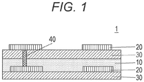
- Fig. 1 is a schematic view showing an example of a cross-section of a multilayer wiring substrate.
- a multilayer wiring substrate of the present disclosure includes a fluororesin substrate having a conductor pattern formed on at least one surface thereof, and an adhesive layer for bonding the fluororesin substrate.
- the adhesive layer contains a cured product of a thermosetting resin, and has a breaking elongation rate of 20% or more and 300% or less.
- Fig. 1 is a schematic view showing an example of a cross-section of the multilayer wiring substrate.
- Fig. 1 shows an example of a cross-section of a two-layer wiring substrate.
- a multilayer wiring substrate 1 shown in Fig. 1 includes a fluororesin substrate 30 having a conductor pattern 20 formed on at least one surface thereof, and an adhesive layer 10 for bonding the fluororesin substrate 30.
- the adhesive layer 10 contains the cured product of the thermosetting resin. Further, the breaking elongation rate of the adhesive layer 10 is 20% or more and 300% or less.
- a via-hole (through-hole) 40 can be formed in the multilayer wiring substrate 1 as required.
- the fluororesin substrate for example, the fluororesin substrate described in JP-A-H07-323501 or JP-A-2005-268365 can be used.
- a specific example is a rigid substrate made of a prepreg, which is obtained by impregnating and holding polytetrafluoroethylene (PTFE) in a glass cloth.
- PTFE polytetrafluoroethylene
- Another example is a so-called paper-making sheet obtained by forming by a wet paper-making method using fluororesin fibers and heat-resistant insulating fibers such as glass fiber.
- fluororesins used for the fluororesin substrate include polytetrafluoroethylene (PTFE), copolymer of tetrafluoroethylene and perfluoroalkyl vinyl ether (PFA), copolymer of tetrafluoroethylene, hexafluoropropylene and perfluoroalkyl vinyl ether (FEPPFA), FEP, polychlorotrifluoroethylene (PCTFE), vinylidene fluoride resin (PVDF), vinyl fluoride resin (PVF), copolymer of ethylene and tetrafluoroethylene (ETFE), and copolymer of ethylene and chlorotrifluoroethylene (ECTFE).
- PTFE polytetrafluoroethylene
- PFA perfluoroalkyl vinyl ether
- FEPPFA hexafluoropropylene and perfluoroalkyl vinyl ether
- FEP fluororesins used for the fluororesin substrate
- PCTFE polychlorotri
- fluororesins PTFE is preferred from the viewpoint of low dielectric constant, low dielectric loss tangent, heat resistance, chemical resistance and the like.
- a melting point of PFA or the like is preferably 280°C or more.
- An example of molding temperature of the fluororesin is 320 to 400°C.
- the fluororesins may be used alone or in combination of two or more.
- heat-resistant insulating fibers include inorganic fibers such as glass fibers, silica fibers, alumina fibers and aluminum silicate fibers, and organic fibers such as polyparaphenylene benzobisoxazole fibers (PBO fibers), aromatic polyester fibers, polyphenylene sulfide fibers and wholly aromatic polyamide fibers.
- the glass fibers are preferred from the viewpoint of heat resistance, high strength, high elastic modulus, and low cost.
- the heat-resistant insulating fibers may be used alone or in combination of two or more.
- the conductor pattern includes copper wiring or the like which is formed by etching of copper foil.
- the adhesive layer contains the cured product of the thermosetting resin.
- the breaking elongation rate of the adhesive layer is 20% or more and 300% or less.
- thermosetting resin imparts adhesiveness and heat resistance (melting resistance at the time of heating) to the adhesive layer.
- the thermosetting resin is not particularly limited as long as it provides the adhesive layer with the breaking elongation rate of 20% or more and 300% or less after thermosetting.
- thermosetting resins include modified polyphenylene ether, bisphenol A epoxy resin, biphenyl epoxy resin, naphthalene epoxy resin, bismaleimide, special acrylate, modified polyimide and the like.
- the resin containing modified polyphenylene ether or modified polyimide is preferred from the viewpoint of the breaking elongation rate and the dielectric constant of the adhesive layer.
- modified polyphenylene ether having an ethylenically unsaturated group (specifically, a styrene group) at its end (for example, one described in JP-A-2004-059644 ) is more preferred since it has high adhesiveness also for small polar fluororesins due to its small polarity.
- the epoxy resins are not preferred because they generally have low breaking elongation rate and high dielectric constant by themselves.
- the thermosetting resins may be used alone or in combination of two or more.
- the epoxy resins as thermosetting resins may require a curing agent.
- the curing agent is not particularly limited. Examples of the curing agents are imidazole-based, amine-based, acid anhydride-based and phenol-based curing agents.
- the imidazole-based curing agents are preferred from the viewpoint of reaction temperature and reaction time. 1-benzyl-2-phenylimidazole and 2-phenyl-4,5-dihydroxymethylimidazole are more preferred.
- the adhesive layer can also contain other resins.
- the other resins are added to improve the breaking elongation rate when the thermosetting resin alone cannot impart the breaking elongation rate of 20% or more to the adhesive layer after thermosetting.
- examples of other resins include polystyrene-poly(ethylene/butylene) block copolymer, polystyrene-poly(ethylene-ethylene/propylene) block co-polymer, and the like, specifically as a styrene-based thermoplastic elastomer among polyolefin-based elastomers. These hydrogenated elastomers are preferred because they have low dielectric constants and low dielectric loss tangents.
- the other resins may be used alone or in combination of two or more.
- the breaking elongation rate of the adhesive layer is preferably 20% or more and 300% or less from the viewpoint of peel strength with the copper foil.
- the breaking elongation rate is less than 20%, the adhesive layer is hard and brittle. Therefore, the peel strength with copper foil is weak.
- the breaking elongation rate exceeds 300%, misalignment is likely to occur during lamination.
- the breaking elongation rate of the adhesive layer can be measured by an autograph.
- the adhesive layer preferably contains a filler having a dielectric loss tangent of 0.002 or less from the viewpoint of further reducing transmission loss of the multilayer wiring substrate.
- the filler having the dielectric loss tangent of 0.002 or less include fluororesin fillers and silica fillers (including hollow silica particles).
- An average particle size of the filler having the dielectric loss tangent of 0.002 or less is preferably 0.01 to 10 ⁇ m, and more preferably 0.01 to 1 ⁇ m.
- the average particle size can be measured by a laser diffraction particle size distribution measuring apparatus (model number: LS13320) produced by Beckman Coulter, Inc.
- the fillers having the dielectric loss tangent of 0.002 or less may be used alone or in combination of two or more.
- Additives can be further added to the adhesive layer of the present embodiment as needed, as long as the purpose of the present embodiment is not impaired.
- the additives include leveling agents, antifoaming agents, thixotropic agents, antioxidants, pigments or dyes.
- a tensile modulus of elasticity of the adhesive layer is preferably 1GPa or less from the viewpoint of internal stress relaxation of the multilayer wiring substrate which is a laminate and the peel strength between the fluororesin and the adhesive layer. Further, the tensile modulus of elasticity of the adhesive layer is preferably 0.1 GPa or more from the viewpoint of pressure resistance at the time of pressing. When the tensile modulus of elasticity is less than 0.1 GPa, the heat resistance (at the time of heat pressing or the like) of the adhesive layer is inferior, and misalignment is likely to occur.
- the dielectric constant of the adhesive layer is preferably 70 to 130%.
- the dielectric constant of the adhesive layer in this range is close to the dielectric constant of the fluororesin substrate. Therefore, design of the multilayer wiring substrate is simplified.
- the transmission loss on the adhesive layer is preferably 0 to -3 dB/70 mm at 20 GHz from the viewpoint of efficient transmission and reception of electrical signals.
- the adhesive layer can be preferably laminated even at a low temperature of 200°C or less from the viewpoint of low power (low energy) and reduction of thermal damage to members.
- the multilayer wiring substrate of the present disclosure includes the fluororesin substrate having the conductor pattern formed on at least one surface thereof, and the adhesive layer for bonding the fluororesin substrate.
- the adhesive layer contains the cured product of the thermosetting resin and has the breaking elongation rate of 20% or more and 300% or less.
- the multilayer wiring substrate is excellent in peel strength between the fluororesin substrate and the adhesive layer, and peel strength between the conductor pattern and the adhesive layer. It is considered that cause of this excellent peel strength is due to an anchor effect. It is considered that the breaking elongation rate of the adhesive layer contributes to the peel strength with the conductor (copper foil). When the breaking elongation rate is less than 20% or more than 300%, the peel strength with the copper foil is weak. Note that since the peel strength between the fluororesin substrate and the adhesive layer is high, peeling may occur between the fluororesin substrate and the copper foil, or the fluororesin substrate itself may be destroyed in a peel test.
- a semiconductor device of the present disclosure includes the above-described multilayer wiring substrate.
- Examples of the semiconductor device include a millimeter wave antenna and a wireless base station.
- thermosetting resin 1 modified polyphenylene ether (product name: OPE2St2200) produced by Mitsubishi Gas Chemical Company, Inc. was used.
- thermosetting resin 2 modified polyphenylene ether (product name: OPE2St1200) produced by Mitsubishi Gas Chemical Company, Inc. was used.
- thermosetting resin 3 bisphenol A epoxy resin (product name: LX-01) produced by Osaka Soda Co., Ltd. was used.
- thermosetting resin 4 biphenyl epoxy resin (product name: NC3000) produced by Nippon Kayaku Co., Ltd. was used.
- thermosetting resin 5 naphthalene epoxy resin (product name: HP4032D) produced by DIC Corporation was used.
- thermosetting resin 6 bis-(3-ethyl-5-methyl-4-maleimidophenyl) methane (product name: BMI-70), which is bismaleimide produced by K ⁇ I Chemical Industry Co., Ltd., was used.
- thermosetting resin 7 N-acryloyloxyethyl hexahydrophthalimide (trade name: M-140), which is a special acrylate produced by Toagosei Co., Ltd., was used.
- imidazole product name: 1B2PZ
- Shikoku Chemicals Corporation was used as a curing agent 1.
- imidazole product name: 2PHZ
- Shikoku Chemicals Corporation was used as a curing agent 2
- elastomer SEBS product name: G1652
- elastomer SEBS product name: G1657
- elastomer SEEPS product name: Septon 4044 produced by Kuraray Co., Ltd. was used.
- elastomer SEBS (trade name: Tuftec H1052) produced by Asahi Kasei Corporation was used.
- elastomer SBS product name: TR2003
- fluororesin filler (trade name: Luburon L-2, average particle size: 2 ⁇ m) produced by Daikin Industries, Ltd. was used.
- silica filler (product name: SE2050, average particle size: 0.5 ⁇ m) produced by Admatechs Co., Ltd. was used.
- dielectric loss tangent of the filler 1 and the dielectric loss tangent of the filler 2 were both 0.002 or less.
- composition shown in Table 1 Components were measured and mixed in composition shown in Table 1. Thereafter, the components were charged into a reaction kettle heated to 80°C, and atmospheric pressure dissolution and mixing were performed for 3 hours while stirring at a rotational speed of 250 rpm. However, the curing agent was added after cooling. Although not shown in Table 1, toluene was used for dissolution and viscosity adjustment.
- a varnish containing the composition for the adhesive layer thus obtained was applied to one side of a support (PET film subjected to release treatment).
- the varnish was dried at 100°C to obtain the film for the adhesive layer with the support (thickness of the adhesive layer: two types of about 25 ⁇ m and about 50 ⁇ m).
- the film for the adhesive layer with the support was vacuum heat-pressed and cured under conditions of 200°C, 60 min and IMPa.
- the film for the adhesive layer with the support after curing was cut out to 15 mm ⁇ 150 mm. After peeling off the support, it was pulled by the autograph at a pulling speed of 200 mm/min in its longitudinal direction, and a length stretched to breakage was measured.
- the breaking elongation rate of the adhesive layer is a value expressed as a percentage, which is obtained by dividing the length at break by the initial length. Table 1 shows measurement results of the breaking elongation rate of the adhesive layer.
- the film for the adhesive layer with the support was vacuum heat-pressed and cured under the conditions of 200°C, 60 min and 1MPa.
- a 25 mm ⁇ 250 mm cured film with the support was cut out from the film for the adhesive layer with the support after curing. After peeling the support from the cured film with the support to obtain a test piece, a thickness of the test piece was measured.
- the test piece was pulled in the longitudinal direction at a pulling speed of 1 mm/min using the autograph. Then, an inclination of stress-strain curve was measured when the test piece was stretched to 1 to 2 mm. This value was divided by a cross-sectional area to determine the tensile modulus of elasticity of the adhesive layer.
- the tensile modulus of elasticity of the adhesive layer is preferably 0.1 to 1GPa or less. Table 1 shows the measurement results of the tensile modulus of elasticity of the adhesive layer.
- the fluororesin substrate (product name: CGS-500) produced by Chukoh Chemical Industries, Ltd. was bonded on one side of the film for the adhesive layer peeled off from the support, and the copper foil (thickness: 35 ⁇ m, product name: CF-T8G-HTE) produced by Fukuda Metal Foil & Powder Co., Ltd. was bonded on the other side thereof, while being vacuum-heat pressed under the conditions of 200°C, 60 min and 2MPa. Thus, a laminated member was prepared. Thereafter, the copper foil or the fluororesin substrate was peeled off by the autograph, to measure the peel strength (90° peel) according to JIS K6854-1. The peel strength is preferably 7 N/cm or more. Table 1 shows the measurement results of the peel strength.
- the laminated member prepared by the same method as the above was floated in a solder bath at 260°C for 1 minute, and the presence or absence of peeling and swelling was visually checked.
- the film for the adhesive layer with the support was vacuum heat-pressed and cured under the conditions of 200°C, 60 min and 1MPa.
- the cured film (70 mm ⁇ 130 mm) with the support was cut out from the film for the adhesive layer with the support after curing. After peeling the support from the cured film with the support to obtain the test piece, the thickness of the test piece was measured.
- the dielectric constant ( ⁇ ) and the dielectric loss tangent (tan ⁇ ) of the test piece were measured by SPDR method (1.9 GHz).
- the dielectric constant is preferably 1.6 to 3.5, and more preferably 2.0 to 2.9.
- the dielectric loss tangent is preferably 0.0005 to 0.005.
- the dielectric constant of the adhesive layer when the dielectric constant of the fluororesin substrate was 100% was calculated.
- the dielectric constant of the fluororesin substrate used was 2.24.
- the dielectric constant of the adhesive layer is preferably 70 to 130%.
- a 50 ⁇ m thick film for the adhesive layer before heat curing was sandwiched between two copper foils (produced by Fukuda Metal Foil & Powder Co., Ltd., 18 ⁇ m, CF-T9FZ-SV), and was then vacuum heat-pressed under the conditions of 200°C, 60 min and 1MPa.
- a copper-clad substrate was produced.
- signal wiring having a signal wiring length of 70 mm and a ground pad were produced by etching so as to have an impedance of 50 ⁇ .
- the other surface of the copper-clad substrate was a ground layer. In order to connect the ground pad and the ground layer, a copper plating process was performed after the through-hole was formed.
- a 50 ⁇ microstrip line substrate was produced.
- a wiring height was about 30 ⁇ m by the copper plating process.
- the produced substrate was measured at 20 GHz using a network analyzer (manufactured by Keysight Technologies, Inc., N5245A).
- a measured value of the obtained S-parameter insertion loss (S21) was defined as the transmission loss on the adhesive layer.
- the transmission loss on the adhesive layer is preferably 0 to -3 dB/70 mm at 20 GHz.
- the breaking elongation rate of the adhesive layer was 50 to 280%
- the tensile modulus of elasticity of the adhesive layer was 0.23 to 0.84GPa
- the peel strength was high.
- the dielectric constant of the adhesive layer was 2.4 to 2.5
- the dielectric loss tangent of the adhesive layer was 0.0008 to 0.0025
- the ratio of the dielectric constant of the fluororesin substrate and the dielectric constant of the adhesive layer was 107 to 112%, and all of them were good.
- the transmission loss of the adhesive layer was -2.2 dB in Example 1, -2.7 dB in Example 2, -2.1 dB in Example 3, and -2.3 dB in Example 4.
- Comparative Examples 1 and 4 in which the breaking elongation rate of the adhesive layer is too low, the peel strength with the copper foil was low.
- Comparative Example 2 in which the breaking elongation rate of the adhesive layer is too high, the peel strength with the fluororesin substrate and the peel strength with the copper foil were both low.
- Comparative Example 3 in which the breaking elongation rate of the adhesive layer is too high, the peel strength with the copper foil was low.
- the transmission loss of the adhesive layer of Comparative Example 1 was -3.6 dB.
- the multilayer wiring substrate of the present disclosure uses the thermosetting resin for suppressing misalignment between layers, and uses the adhesive layer excellent in peel strength, the transmission loss of the electrical signals is low when using the fluororesin substrate. Therefore, the multilayer wiring substrate of the present disclosure is very useful.
- Multilayer wiring substrate 10: Adhesive layer, 20: Conductor pattern, 30: Fluororesin substrate, 40: Via-hole (Through-hole).
Landscapes
- Chemical & Material Sciences (AREA)
- Organic Chemistry (AREA)
- Engineering & Computer Science (AREA)
- Microelectronics & Electronic Packaging (AREA)
- Manufacturing & Machinery (AREA)
- Inorganic Chemistry (AREA)
- Laminated Bodies (AREA)
- Production Of Multi-Layered Print Wiring Board (AREA)
- Adhesives Or Adhesive Processes (AREA)
- Adhesive Tapes (AREA)
Abstract
Description
- The present disclosure relates to a multilayer wiring substrate and a semiconductor device.
- In recent years, with progress of miniaturization and high performance of electronic devices, there is a need for further speeding up of electrical signals used for information transmission. When transmitting high speed electrical signals, signal loss occurs. As the electrical signals get faster, the signal loss increases. As a technique of reducing the signal loss, a fluororesin substrate is generally used for circuit materials.
- Further, with high functionality of parts, the circuit materials of a circuit substrate or the like, specifically, those of the multilayer wiring substrate suitable for high frequency circuits have been highly multilayered. Conventionally, in order to form a multilayer, a thermoplastic resin having a low dielectric constant and a low dielectric loss tangent (excellent in high frequency characteristics) is used as an adhesive layer.
- As a multilayer fluororesin substrate, a copper-clad laminate including a copper foil bonded to a fluororesin insulating substrate is known. A feature of the copper-clad laminate is that the copper foil with smooth surfaces on both sides, which is neither roughened nor blackened, is bonded to the insulating substrate through a composite film of LCP and PFA (PATENT LITERATURE 1). A multilayer printed circuit substrate is also reported, which is formed of a plurality of laminated fluorocarbon resin-based base layers and includes at least one conductor layer therein (PATENT LITERATURE 2). A feature of the circuit substrate is that a base material layer including the above-mentioned inner conductor layer and a base material layer adjacent thereto are bonded to each other through the adhesive layer made of liquid crystal polymer.
- However, in general, when the thermoplastic resin is used for the circuit substrate, there is a problem that misalignment occurs between layers when repeatedly heated to form the multilayer. It is possible to suppress misalignment by using a jig. However, minute misalignment cannot be prevented.
- Specifically, the liquid crystal polymer (LCP) having a high melting point are used for both the copper-clad laminate and the multilayer printed circuit substrate described above. Therefore, phenomenon of misalignment between layers is aggravated. As a result, multilayering is more difficult.
-
- PATENT LITERATURE 1:
JP-A-2007-098692 - PATENT LITERATURE 2:
JP-A-2005-268365 - The inventors of the present invention have conducted intensive studies, to obtain the multilayer wiring substrate capable of reducing transmission loss of the electrical signals when using the fluororesin substrate by using the adhesive layer capable of suppressing misalignment between layers and having excellent peel strength.
- An object of the present disclosure is to provide the multilayer wiring substrate capable of reducing the transmission loss of the electrical signals when using the fluororesin substrate by using the adhesive layer capable of suppressing misalignment between layers and having excellent peel strength, and the semiconductor device using the same.
- The present disclosure relates to the multilayer wiring substrate and the semiconductor device, which can solve the above problems by having the following configurations.
- [1] A multilayer wiring substrate including: a fluororesin substrate having a conductor pattern formed on at least one surface thereof; and an adhesive layer for bonding the fluororesin substrate, wherein the adhesive layer contains a cured product of a thermosetting resin, and has a breaking elongation rate of 20% or more and 300% or less.
- [2] The multilayer wiring substrate according to the above [1], wherein a tensile modulus of elasticity of the adhesive layer is 1GPa or less.
- [3] The multilayer wiring substrate according to the above [1] or [2], wherein the adhesive layer includes a filler having a dielectric loss tangent of 0.002 or less.
- [4] The multilayer wiring substrate according to any one of the above [1] to [3], wherein a dielectric constant of the adhesive layer is 70 to 130% when the dielectric constant of the fluororesin substrate is 100%.
- [5] The multilayer wiring substrate according to any one of the above [1] to [4], wherein transmission loss on the adhesive layer is 0 to -3 dB/70 mm at 20 GHz.
- [6] A semiconductor device including the multilayer wiring substrate according to any one of the above [1] to [5].
- According to the present disclosure [1], it is possible to provide a multilayer wiring substrate capable of reducing the transmission loss of the electrical signals when using a fluororesin substrate, by using an adhesive layer capable of suppressing misalignment between layers and having excellent peel strength.
- According to the present disclosure [6], it is possible to provide a high reliability semiconductor component including the multilayer wiring substrate capable of reducing the transmission loss of the electrical signals by the adhesive layer capable of suppressing misalignment between layers and having excellent peel strength.
-
Fig. 1 is a schematic view showing an example of a cross-section of a multilayer wiring substrate. - A multilayer wiring substrate of the present disclosure includes a fluororesin substrate having a conductor pattern formed on at least one surface thereof, and an adhesive layer for bonding the fluororesin substrate. The adhesive layer contains a cured product of a thermosetting resin, and has a breaking elongation rate of 20% or more and 300% or less.
Fig. 1 is a schematic view showing an example of a cross-section of the multilayer wiring substrate.Fig. 1 shows an example of a cross-section of a two-layer wiring substrate. A multilayer wiring substrate 1 shown inFig. 1 includes afluororesin substrate 30 having aconductor pattern 20 formed on at least one surface thereof, and anadhesive layer 10 for bonding thefluororesin substrate 30. Theadhesive layer 10 contains the cured product of the thermosetting resin. Further, the breaking elongation rate of theadhesive layer 10 is 20% or more and 300% or less. - As shown in
Fig. 1 , a via-hole (through-hole) 40 can be formed in the multilayer wiring substrate 1 as required. - As the fluororesin substrate, for example, the fluororesin substrate described in
JP-A-H07-323501 JP-A-2005-268365 - Examples of fluororesins used for the fluororesin substrate include polytetrafluoroethylene (PTFE), copolymer of tetrafluoroethylene and perfluoroalkyl vinyl ether (PFA), copolymer of tetrafluoroethylene, hexafluoropropylene and perfluoroalkyl vinyl ether (FEPPFA), FEP, polychlorotrifluoroethylene (PCTFE), vinylidene fluoride resin (PVDF), vinyl fluoride resin (PVF), copolymer of ethylene and tetrafluoroethylene (ETFE), and copolymer of ethylene and chlorotrifluoroethylene (ECTFE). Among the fluororesins, PTFE is preferred from the viewpoint of low dielectric constant, low dielectric loss tangent, heat resistance, chemical resistance and the like. A melting point of PFA or the like is preferably 280°C or more. An example of molding temperature of the fluororesin is 320 to 400°C. The fluororesins may be used alone or in combination of two or more.
- Examples of heat-resistant insulating fibers include inorganic fibers such as glass fibers, silica fibers, alumina fibers and aluminum silicate fibers, and organic fibers such as polyparaphenylene benzobisoxazole fibers (PBO fibers), aromatic polyester fibers, polyphenylene sulfide fibers and wholly aromatic polyamide fibers. The glass fibers are preferred from the viewpoint of heat resistance, high strength, high elastic modulus, and low cost. The heat-resistant insulating fibers may be used alone or in combination of two or more.
- The conductor pattern includes copper wiring or the like which is formed by etching of copper foil.
- The adhesive layer contains the cured product of the thermosetting resin. The breaking elongation rate of the adhesive layer is 20% or more and 300% or less.
- The thermosetting resin imparts adhesiveness and heat resistance (melting resistance at the time of heating) to the adhesive layer. The thermosetting resin is not particularly limited as long as it provides the adhesive layer with the breaking elongation rate of 20% or more and 300% or less after thermosetting. Examples of thermosetting resins include modified polyphenylene ether, bisphenol A epoxy resin, biphenyl epoxy resin, naphthalene epoxy resin, bismaleimide, special acrylate, modified polyimide and the like. The resin containing modified polyphenylene ether or modified polyimide is preferred from the viewpoint of the breaking elongation rate and the dielectric constant of the adhesive layer. Specifically, modified polyphenylene ether having an ethylenically unsaturated group (specifically, a styrene group) at its end (for example, one described in
JP-A-2004-059644 - The epoxy resins as thermosetting resins may require a curing agent. The curing agent is not particularly limited. Examples of the curing agents are imidazole-based, amine-based, acid anhydride-based and phenol-based curing agents. The imidazole-based curing agents are preferred from the viewpoint of reaction temperature and reaction time. 1-benzyl-2-phenylimidazole and 2-phenyl-4,5-dihydroxymethylimidazole are more preferred.
- The adhesive layer can also contain other resins. The other resins are added to improve the breaking elongation rate when the thermosetting resin alone cannot impart the breaking elongation rate of 20% or more to the adhesive layer after thermosetting. Examples of other resins include polystyrene-poly(ethylene/butylene) block copolymer, polystyrene-poly(ethylene-ethylene/propylene) block co-polymer, and the like, specifically as a styrene-based thermoplastic elastomer among polyolefin-based elastomers. These hydrogenated elastomers are preferred because they have low dielectric constants and low dielectric loss tangents. The other resins may be used alone or in combination of two or more.
- The breaking elongation rate of the adhesive layer is preferably 20% or more and 300% or less from the viewpoint of peel strength with the copper foil. When the breaking elongation rate is less than 20%, the adhesive layer is hard and brittle. Therefore, the peel strength with copper foil is weak. When the breaking elongation rate exceeds 300%, misalignment is likely to occur during lamination. Here, the breaking elongation rate of the adhesive layer can be measured by an autograph.
- The adhesive layer preferably contains a filler having a dielectric loss tangent of 0.002 or less from the viewpoint of further reducing transmission loss of the multilayer wiring substrate. Examples of the filler having the dielectric loss tangent of 0.002 or less include fluororesin fillers and silica fillers (including hollow silica particles). An average particle size of the filler having the dielectric loss tangent of 0.002 or less is preferably 0.01 to 10 µm, and more preferably 0.01 to 1 µm. Here, the average particle size can be measured by a laser diffraction particle size distribution measuring apparatus (model number: LS13320) produced by Beckman Coulter, Inc. The fillers having the dielectric loss tangent of 0.002 or less may be used alone or in combination of two or more.
- Additives can be further added to the adhesive layer of the present embodiment as needed, as long as the purpose of the present embodiment is not impaired. Examples of the additives include leveling agents, antifoaming agents, thixotropic agents, antioxidants, pigments or dyes.
- A tensile modulus of elasticity of the adhesive layer is preferably 1GPa or less from the viewpoint of internal stress relaxation of the multilayer wiring substrate which is a laminate and the peel strength between the fluororesin and the adhesive layer. Further, the tensile modulus of elasticity of the adhesive layer is preferably 0.1 GPa or more from the viewpoint of pressure resistance at the time of pressing. When the tensile modulus of elasticity is less than 0.1 GPa, the heat resistance (at the time of heat pressing or the like) of the adhesive layer is inferior, and misalignment is likely to occur.
- When the dielectric constant of the fluororesin substrate is 100%, the dielectric constant of the adhesive layer is preferably 70 to 130%. The dielectric constant of the adhesive layer in this range is close to the dielectric constant of the fluororesin substrate. Therefore, design of the multilayer wiring substrate is simplified.
- The transmission loss on the adhesive layer is preferably 0 to -3 dB/70 mm at 20 GHz from the viewpoint of efficient transmission and reception of electrical signals.
- The adhesive layer can be preferably laminated even at a low temperature of 200°C or less from the viewpoint of low power (low energy) and reduction of thermal damage to members.
- As described above, the multilayer wiring substrate of the present disclosure includes the fluororesin substrate having the conductor pattern formed on at least one surface thereof, and the adhesive layer for bonding the fluororesin substrate. The adhesive layer contains the cured product of the thermosetting resin and has the breaking elongation rate of 20% or more and 300% or less. The multilayer wiring substrate is excellent in peel strength between the fluororesin substrate and the adhesive layer, and peel strength between the conductor pattern and the adhesive layer. It is considered that cause of this excellent peel strength is due to an anchor effect. It is considered that the breaking elongation rate of the adhesive layer contributes to the peel strength with the conductor (copper foil). When the breaking elongation rate is less than 20% or more than 300%, the peel strength with the copper foil is weak. Note that since the peel strength between the fluororesin substrate and the adhesive layer is high, peeling may occur between the fluororesin substrate and the copper foil, or the fluororesin substrate itself may be destroyed in a peel test.
- A semiconductor device of the present disclosure includes the above-described multilayer wiring substrate. Examples of the semiconductor device include a millimeter wave antenna and a wireless base station.
- The present embodiment will be described by way of examples. However, the present embodiment is not limited to the examples. In the following examples, parts and % respectively indicate parts by mass and % by mass unless otherwise specified.
- As a thermosetting resin 1, modified polyphenylene ether (product name: OPE2St2200) produced by Mitsubishi Gas Chemical Company, Inc. was used.
- As a thermosetting resin 2, modified polyphenylene ether (product name: OPE2St1200) produced by Mitsubishi Gas Chemical Company, Inc. was used.
- As a thermosetting resin 3, bisphenol A epoxy resin (product name: LX-01) produced by Osaka Soda Co., Ltd. was used.
- As a thermosetting resin 4, biphenyl epoxy resin (product name: NC3000) produced by Nippon Kayaku Co., Ltd. was used.
- As a thermosetting resin 5, naphthalene epoxy resin (product name: HP4032D) produced by DIC Corporation was used.
- As a thermosetting resin 6, bis-(3-ethyl-5-methyl-4-maleimidophenyl) methane (product name: BMI-70), which is bismaleimide produced by K·I Chemical Industry Co., Ltd., was used.
- As a thermosetting resin 7, N-acryloyloxyethyl hexahydrophthalimide (trade name: M-140), which is a special acrylate produced by Toagosei Co., Ltd., was used.
- As a curing agent 1, imidazole (product name: 1B2PZ) produced by Shikoku Chemicals Corporation was used.
- As a curing agent 2, imidazole (product name: 2PHZ) produced by Shikoku Chemicals Corporation was used.
- As another resin 1, elastomer SEBS (product name: G1652) produced by Kraton Corporation was used.
- As another resin 2, elastomer SEBS (product name: G1657) produced by Kraton Corporation was used.
- As another resin 3, elastomer SEEPS (product name: Septon 4044) produced by Kuraray Co., Ltd. was used.
- As another resin 4, elastomer SEBS (trade name: Tuftec H1052) produced by Asahi Kasei Corporation was used.
- As another resin 5, elastomer SBS (product name: TR2003) produced by JSR Corporation was used.
- As a filler 1, fluororesin filler (trade name: Luburon L-2, average particle size: 2 µm) produced by Daikin Industries, Ltd. was used.
- As a filler 2, silica filler (product name: SE2050, average particle size: 0.5 µm) produced by Admatechs Co., Ltd. was used.
- Note that the dielectric loss tangent of the filler 1 and the dielectric loss tangent of the filler 2 were both 0.002 or less.
- Components were measured and mixed in composition shown in Table 1. Thereafter, the components were charged into a reaction kettle heated to 80°C, and atmospheric pressure dissolution and mixing were performed for 3 hours while stirring at a rotational speed of 250 rpm. However, the curing agent was added after cooling. Although not shown in Table 1, toluene was used for dissolution and viscosity adjustment.
- A varnish containing the composition for the adhesive layer thus obtained was applied to one side of a support (PET film subjected to release treatment). The varnish was dried at 100°C to obtain the film for the adhesive layer with the support (thickness of the adhesive layer: two types of about 25 µm and about 50 µm).
- The film for the adhesive layer with the support was vacuum heat-pressed and cured under conditions of 200°C, 60 min and IMPa. The film for the adhesive layer with the support after curing was cut out to 15 mm×150 mm. After peeling off the support, it was pulled by the autograph at a pulling speed of 200 mm/min in its longitudinal direction, and a length stretched to breakage was measured. The breaking elongation rate of the adhesive layer is a value expressed as a percentage, which is obtained by dividing the length at break by the initial length. Table 1 shows measurement results of the breaking elongation rate of the adhesive layer.
- The film for the adhesive layer with the support was vacuum heat-pressed and cured under the conditions of 200°C, 60 min and 1MPa. A 25 mm×250 mm cured film with the support was cut out from the film for the adhesive layer with the support after curing. After peeling the support from the cured film with the support to obtain a test piece, a thickness of the test piece was measured. Next, the test piece was pulled in the longitudinal direction at a pulling speed of 1 mm/min using the autograph. Then, an inclination of stress-strain curve was measured when the test piece was stretched to 1 to 2 mm. This value was divided by a cross-sectional area to determine the tensile modulus of elasticity of the adhesive layer. The tensile modulus of elasticity of the adhesive layer is preferably 0.1 to 1GPa or less. Table 1 shows the measurement results of the tensile modulus of elasticity of the adhesive layer.
- The fluororesin substrate (product name: CGS-500) produced by Chukoh Chemical Industries, Ltd. was bonded on one side of the film for the adhesive layer peeled off from the support, and the copper foil (thickness: 35 µm, product name: CF-T8G-HTE) produced by Fukuda Metal Foil & Powder Co., Ltd. was bonded on the other side thereof, while being vacuum-heat pressed under the conditions of 200°C, 60 min and 2MPa. Thus, a laminated member was prepared. Thereafter, the copper foil or the fluororesin substrate was peeled off by the autograph, to measure the peel strength (90° peel) according to JIS K6854-1. The peel strength is preferably 7 N/cm or more. Table 1 shows the measurement results of the peel strength.
- The laminated member prepared by the same method as the above was floated in a solder bath at 260°C for 1 minute, and the presence or absence of peeling and swelling was visually checked.
- The film for the adhesive layer with the support was vacuum heat-pressed and cured under the conditions of 200°C, 60 min and 1MPa. The cured film (70 mm×130 mm) with the support was cut out from the film for the adhesive layer with the support after curing. After peeling the support from the cured film with the support to obtain the test piece, the thickness of the test piece was measured. Next, the dielectric constant (ε) and the dielectric loss tangent (tan δ) of the test piece were measured by SPDR method (1.9 GHz). The dielectric constant is preferably 1.6 to 3.5, and more preferably 2.0 to 2.9. The dielectric loss tangent is preferably 0.0005 to 0.005.
- Next, a ratio (unit: %) of the dielectric constant of the adhesive layer when the dielectric constant of the fluororesin substrate was 100% was calculated. The dielectric constant of the fluororesin substrate used was 2.24. When the dielectric constant of the fluororesin substrate is 100%, the dielectric constant of the adhesive layer is preferably 70 to 130%.
- After removing the support, a 50 µm thick film for the adhesive layer before heat curing was sandwiched between two copper foils (produced by Fukuda Metal Foil & Powder Co., Ltd., 18 µm, CF-T9FZ-SV), and was then vacuum heat-pressed under the conditions of 200°C, 60 min and 1MPa. Thus, a copper-clad substrate was produced. On one surface of the copper-clad substrate, signal wiring having a signal wiring length of 70 mm and a ground pad were produced by etching so as to have an impedance of 50 Ω. The other surface of the copper-clad substrate was a ground layer. In order to connect the ground pad and the ground layer, a copper plating process was performed after the through-hole was formed. Thus, a 50 Ω microstrip line substrate was produced. At this time, a wiring height was about 30 µm by the copper plating process. The produced substrate was measured at 20 GHz using a network analyzer (manufactured by Keysight Technologies, Inc., N5245A). A measured value of the obtained S-parameter insertion loss (S21) was defined as the transmission loss on the adhesive layer. The transmission loss on the adhesive layer is preferably 0 to -3 dB/70 mm at 20 GHz.

- As can be seen from Table 1, in all of Examples 1 to 4 using a thermosetting resin which does not cause misalignment between layers, the breaking elongation rate of the adhesive layer was 50 to 280%, the tensile modulus of elasticity of the adhesive layer was 0.23 to 0.84GPa, and the peel strength was high. Although not shown in Table 1, in all of Examples 1 to 4, not only the heat resistance is good, but the dielectric constant of the adhesive layer was 2.4 to 2.5, the dielectric loss tangent of the adhesive layer was 0.0008 to 0.0025, the ratio of the dielectric constant of the fluororesin substrate and the dielectric constant of the adhesive layer was 107 to 112%, and all of them were good. The transmission loss of the adhesive layer was -2.2 dB in Example 1, -2.7 dB in Example 2, -2.1 dB in Example 3, and -2.3 dB in Example 4. In contrast, in Comparative Examples 1 and 4 in which the breaking elongation rate of the adhesive layer is too low, the peel strength with the copper foil was low. In Comparative Example 2 in which the breaking elongation rate of the adhesive layer is too high, the peel strength with the fluororesin substrate and the peel strength with the copper foil were both low. In Comparative Example 3 in which the breaking elongation rate of the adhesive layer is too high, the peel strength with the copper foil was low. Although not shown in Table 1, the transmission loss of the adhesive layer of Comparative Example 1 was -3.6 dB.
- As described above, since the multilayer wiring substrate of the present disclosure uses the thermosetting resin for suppressing misalignment between layers, and uses the adhesive layer excellent in peel strength, the transmission loss of the electrical signals is low when using the fluororesin substrate. Therefore, the multilayer wiring substrate of the present disclosure is very useful.
- 1: Multilayer wiring substrate, 10: Adhesive layer, 20: Conductor pattern, 30: Fluororesin substrate, 40: Via-hole (Through-hole).
Claims (6)
- A multilayer wiring substrate comprising:a fluororesin substrate having a conductor pattern formed on at least one surface thereof; andan adhesive layer for bonding the fluororesin substrate, whereinthe adhesive layer contains a cured product of a thermosetting resin, and has a breaking elongation rate of 20% or more and 300% or less.
- The multilayer wiring substrate according to claim 1, wherein a tensile modulus of elasticity of the adhesive layer is 1GPa or less.
- The multilayer wiring substrate according to claim 1 or 2, wherein the adhesive layer includes a filler having a dielectric loss tangent of 0.002 or less.
- The multilayer wiring substrate according to any one of claims 1 to 3, wherein a dielectric constant of the adhesive layer is 70 to 130% when the dielectric constant of the fluororesin substrate is 100%.
- The multilayer wiring substrate according to any one of claims 1 to 4, wherein transmission loss on the adhesive layer is 0 to -3 dB/70 mm at 20 GHz.
- A semiconductor device comprising the multilayer wiring substrate according to any one of claims 1 to 5.
Applications Claiming Priority (2)
| Application Number | Priority Date | Filing Date | Title |
|---|---|---|---|
| JP2017031408 | 2017-02-22 | ||
| PCT/JP2018/005932 WO2018155418A1 (en) | 2017-02-22 | 2018-02-20 | Multi-layer wiring substrate and semiconductor device |
Publications (2)
| Publication Number | Publication Date |
|---|---|
| EP3589093A1 true EP3589093A1 (en) | 2020-01-01 |
| EP3589093A4 EP3589093A4 (en) | 2020-12-23 |
Family
ID=63253893
Family Applications (1)
| Application Number | Title | Priority Date | Filing Date |
|---|---|---|---|
| EP18756912.4A Pending EP3589093A4 (en) | 2017-02-22 | 2018-02-20 | MULTI-LAYER WIRING SUBSTRATE AND SEMICONDUCTOR COMPONENT |
Country Status (7)
| Country | Link |
|---|---|
| US (1) | US20200058577A1 (en) |
| EP (1) | EP3589093A4 (en) |
| JP (3) | JP7148146B2 (en) |
| KR (2) | KR102566108B1 (en) |
| CN (1) | CN110249715B (en) |
| TW (1) | TWI818904B (en) |
| WO (1) | WO2018155418A1 (en) |
Families Citing this family (11)
| Publication number | Priority date | Publication date | Assignee | Title |
|---|---|---|---|---|
| JP7529392B2 (en) * | 2019-10-29 | 2024-08-06 | 日鉄ケミカル&マテリアル株式会社 | Silica particles, resin composition, resin film and metal-clad laminate |
| JP7824027B2 (en) * | 2019-10-29 | 2026-03-04 | 株式会社レゾナック | Fluororesin substrate laminate |
| CN115397940B (en) * | 2020-03-31 | 2025-02-14 | 琳得科株式会社 | Adhesive for high frequency dielectric heating, structure and method for manufacturing the structure |
| JP7478031B2 (en) | 2020-06-02 | 2024-05-02 | 信越化学工業株式会社 | Manufacturing method of low dielectric silica powder |
| US20230299461A1 (en) * | 2020-07-03 | 2023-09-21 | Namics Corporation | Antenna-equipped semiconductor package and resin composition for antenna-equipped semiconductor package |
| JP2022050927A (en) * | 2020-09-18 | 2022-03-31 | 住友ベークライト株式会社 | Resin film with metallic foil and method for manufacturing substrate for high frequency circuit |
| JPWO2022210673A1 (en) * | 2021-03-30 | 2022-10-06 | ||
| JP7786044B2 (en) * | 2021-04-28 | 2025-12-16 | 株式会社レゾナック | Fluororesin substrate laminate and method for manufacturing the same |
| JPWO2024204006A1 (en) * | 2023-03-30 | 2024-10-03 | ||
| KR20260020377A (en) * | 2023-06-08 | 2026-02-11 | 에이지씨 가부시키가이샤 | Resin-attached metal foil |
| JP2025096895A (en) * | 2023-12-18 | 2025-06-30 | artience株式会社 | Adhesive sheet for printed wiring boards, metal-clad laminate, printed wiring board, and electronic device |
Family Cites Families (24)
| Publication number | Priority date | Publication date | Assignee | Title |
|---|---|---|---|---|
| JP2614190B2 (en) | 1994-06-01 | 1997-05-28 | 日本ピラー工業株式会社 | Prepreg for multilayer board, laminated board, multilayer printed circuit board and method of manufacturing the same |
| JP2001203466A (en) * | 2000-01-20 | 2001-07-27 | Nippon Shokubai Co Ltd | Multilayer printed circuit board |
| JP2003133814A (en) * | 2001-10-24 | 2003-05-09 | Kyocera Corp | High frequency wiring board |
| JP2003298196A (en) * | 2002-04-03 | 2003-10-17 | Japan Gore Tex Inc | Dielectric film for printed wiring board, multilayer printed circuit board, and semiconductor device |
| JP4038667B2 (en) | 2002-07-25 | 2008-01-30 | 三菱瓦斯化学株式会社 | Vinyl compounds and cured products thereof |
| JP4325337B2 (en) * | 2003-09-19 | 2009-09-02 | 日立化成工業株式会社 | Resin composition, prepreg, laminate and multilayer printed wiring board using the same |
| JP2005174161A (en) * | 2003-12-15 | 2005-06-30 | Konica Minolta Photo Imaging Inc | Ic card and manufacturing method for ic card |
| JP2005268365A (en) | 2004-03-17 | 2005-09-29 | Nippon Pillar Packing Co Ltd | Multilayer printed circuit board and method for manufacturing the same |
| JP2006024618A (en) * | 2004-07-06 | 2006-01-26 | Toshiba Corp | Wiring board |
| JP4917745B2 (en) * | 2004-08-17 | 2012-04-18 | ユニチカ株式会社 | High frequency substrate and manufacturing method thereof |
| JP4377867B2 (en) * | 2005-09-30 | 2009-12-02 | 日本ピラー工業株式会社 | Copper-clad laminate, printed wiring board, multilayer printed wiring board, and methods for producing them |
| US20090239992A1 (en) * | 2006-08-08 | 2009-09-24 | Toshiaki Yamada | Thermosetting resin composition and uncured film comprising the same |
| JP5023623B2 (en) * | 2006-08-31 | 2012-09-12 | 東亞合成株式会社 | Halogen-free flame retardant adhesive composition |
| JP2011011456A (en) * | 2009-07-02 | 2011-01-20 | Toyobo Co Ltd | Multilayered fluoroplastic film, and multilayered fluoroplastic substrate |
| GB201102672D0 (en) * | 2011-02-15 | 2011-03-30 | Zephyros Inc | Improved structural adhesives |
| JP2012243923A (en) * | 2011-05-19 | 2012-12-10 | Fujikura Ltd | Flexible printed circuit and manufacturing method thereof |
| JP6034019B2 (en) * | 2011-12-21 | 2016-11-30 | リンテック株式会社 | Dicing sheet with protective film forming layer and chip manufacturing method |
| JP2014207297A (en) * | 2013-04-11 | 2014-10-30 | 株式会社フジクラ | Flexible printed circuit, and method for manufacturing the same |
| WO2014192322A1 (en) * | 2013-05-31 | 2014-12-04 | 住友電気工業株式会社 | High-frequency printed circuit board and wiring material |
| WO2015053309A1 (en) * | 2013-10-11 | 2015-04-16 | 住友電工プリントサーキット株式会社 | Fluorine resin base material, printed wiring board, and circuit module |
| US10559505B2 (en) * | 2014-01-22 | 2020-02-11 | Lintec Corporation | Protective film-forming film, sheet for forming protective film, complex sheet for forming protective film, and inspection method |
| JP2016124982A (en) * | 2014-12-27 | 2016-07-11 | 新日鉄住金化学株式会社 | Crosslinked polyimide resin, production method thereof, adhesive resin composition, cured product thereof, coverlay film, and circuit board |
| WO2016117554A1 (en) * | 2015-01-19 | 2016-07-28 | 株式会社巴川製紙所 | Thermosetting adhesive composition, thermosetting adhesive film, and composite film |
| JP6017750B1 (en) * | 2015-03-23 | 2016-11-02 | タツタ電線株式会社 | Manufacturing method of resin impregnated material, composite material and copper clad laminate |
-
2018
- 2018-02-20 KR KR1020227041841A patent/KR102566108B1/en active Active
- 2018-02-20 EP EP18756912.4A patent/EP3589093A4/en active Pending
- 2018-02-20 JP JP2019501329A patent/JP7148146B2/en active Active
- 2018-02-20 KR KR1020197023434A patent/KR102473321B1/en active Active
- 2018-02-20 WO PCT/JP2018/005932 patent/WO2018155418A1/en not_active Ceased
- 2018-02-20 US US16/487,929 patent/US20200058577A1/en not_active Abandoned
- 2018-02-20 CN CN201880010156.4A patent/CN110249715B/en active Active
- 2018-02-22 TW TW107105908A patent/TWI818904B/en active
-
2022
- 2022-04-20 JP JP2022069235A patent/JP7313736B2/en active Active
-
2023
- 2023-07-05 JP JP2023110420A patent/JP2023126302A/en not_active Withdrawn
Also Published As
| Publication number | Publication date |
|---|---|
| JP7313736B2 (en) | 2023-07-25 |
| EP3589093A4 (en) | 2020-12-23 |
| US20200058577A1 (en) | 2020-02-20 |
| TW201843047A (en) | 2018-12-16 |
| CN110249715B (en) | 2022-08-23 |
| KR102566108B1 (en) | 2023-08-11 |
| KR20220164623A (en) | 2022-12-13 |
| TWI818904B (en) | 2023-10-21 |
| WO2018155418A1 (en) | 2018-08-30 |
| CN110249715A (en) | 2019-09-17 |
| JP2022115868A (en) | 2022-08-09 |
| KR20190121298A (en) | 2019-10-25 |
| JP7148146B2 (en) | 2022-10-05 |
| JPWO2018155418A1 (en) | 2019-12-12 |
| KR102473321B1 (en) | 2022-12-01 |
| JP2023126302A (en) | 2023-09-07 |
Similar Documents
| Publication | Publication Date | Title |
|---|---|---|
| JP7313736B2 (en) | Films for adhesive layers, multilayer wiring boards, and semiconductor devices | |
| JP6572983B2 (en) | Epoxy resin composition | |
| TWI466970B (en) | Cyanate esters based adhesive resin composition for manufacturing circuit board and flexible metal clad laminate comprising the same | |
| CN103650649B (en) | Adhesive film, multilayer printed circuit board using the adhesive film, and method for manufacturing the multilayer printed circuit board | |
| TWI677528B (en) | Thermosetting epoxy resin composition for insulating layer of multilayer printed wiring board, adhesive film for insulating layer of multilayer printed wiring board, and multilayer printed wiring board | |
| CN108141967B (en) | Manufacturing method of wiring board | |
| CN113243146B (en) | Method for manufacturing semiconductor element mounting package substrate | |
| US20250386435A1 (en) | Roll-type flexible metal laminate, method for manufacturing the same, and printed circuit board comprising the flexible metal laminate | |
| KR102254212B1 (en) | Polyolefin based adhesive composition having excellent low dielectric feature, bonding sheet, printed circuit board and method for preparing the same | |
| CN101107891A (en) | Multilayer printed wiring board | |
| WO2014192322A1 (en) | High-frequency printed circuit board and wiring material | |
| JP2011105911A (en) | Epoxy resin composition containing silicone rubber fine particle, prepreg, metal-clad laminate, printed wiring board, and semiconductor device | |
| KR20230168407A (en) | Adhesive composition for insulating film, insulating film sheet and method for manufacturing printed wiring board | |
| WO2020059606A1 (en) | Laminate, printed board, and method for manufacturing same | |
| TW202603091A (en) | Next, thin films, wiring boards, multilayer wiring boards, and semiconductor devices are used. | |
| JPH10326952A (en) | Wiring board materials and wiring boards | |
| JP2005186285A (en) | Insulating film and multilayer wiring board using the same | |
| JPH11135901A (en) | Wiring board materials and printed wiring boards | |
| JP2004311674A (en) | Multilayer wiring board and method of manufacturing the same |
Legal Events
| Date | Code | Title | Description |
|---|---|---|---|
| STAA | Information on the status of an ep patent application or granted ep patent |
Free format text: STATUS: THE INTERNATIONAL PUBLICATION HAS BEEN MADE |
|
| PUAI | Public reference made under article 153(3) epc to a published international application that has entered the european phase |
Free format text: ORIGINAL CODE: 0009012 |
|
| STAA | Information on the status of an ep patent application or granted ep patent |
Free format text: STATUS: REQUEST FOR EXAMINATION WAS MADE |
|
| 17P | Request for examination filed |
Effective date: 20190920 |
|
| AK | Designated contracting states |
Kind code of ref document: A1 Designated state(s): AL AT BE BG CH CY CZ DE DK EE ES FI FR GB GR HR HU IE IS IT LI LT LU LV MC MK MT NL NO PL PT RO RS SE SI SK SM TR |
|
| AX | Request for extension of the european patent |
Extension state: BA ME |
|
| DAV | Request for validation of the european patent (deleted) | ||
| DAX | Request for extension of the european patent (deleted) | ||
| RIN1 | Information on inventor provided before grant (corrected) |
Inventor name: YOSHIDA, MASAKI Inventor name: OHASHI, SATOKO |
|
| A4 | Supplementary search report drawn up and despatched |
Effective date: 20201124 |
|
| RIC1 | Information provided on ipc code assigned before grant |
Ipc: H01L 23/12 20060101ALI20201118BHEP Ipc: B32B 15/082 20060101ALI20201118BHEP Ipc: C09J 11/04 20060101ALI20201118BHEP Ipc: C09J 201/00 20060101ALI20201118BHEP Ipc: C09J 7/20 20180101ALI20201118BHEP Ipc: H05K 1/02 20060101ALN20201118BHEP Ipc: C09J 11/06 20060101ALI20201118BHEP Ipc: H05K 3/46 20060101AFI20201118BHEP Ipc: H05K 1/03 20060101ALI20201118BHEP |
|
| STAA | Information on the status of an ep patent application or granted ep patent |
Free format text: STATUS: EXAMINATION IS IN PROGRESS |
|
| 17Q | First examination report despatched |
Effective date: 20230118 |