EP3588785A1 - Symbol mapping device - Google Patents
Symbol mapping device Download PDFInfo
- Publication number
- EP3588785A1 EP3588785A1 EP17901814.8A EP17901814A EP3588785A1 EP 3588785 A1 EP3588785 A1 EP 3588785A1 EP 17901814 A EP17901814 A EP 17901814A EP 3588785 A1 EP3588785 A1 EP 3588785A1
- Authority
- EP
- European Patent Office
- Prior art keywords
- data
- bits
- parity
- transmission data
- bit
- Prior art date
- Legal status (The legal status is an assumption and is not a legal conclusion. Google has not performed a legal analysis and makes no representation as to the accuracy of the status listed.)
- Granted
Links
Images



Classifications
-
- H—ELECTRICITY
- H03—ELECTRONIC CIRCUITRY
- H03M—CODING; DECODING; CODE CONVERSION IN GENERAL
- H03M13/00—Coding, decoding or code conversion, for error detection or error correction; Coding theory basic assumptions; Coding bounds; Error probability evaluation methods; Channel models; Simulation or testing of codes
- H03M13/03—Error detection or forward error correction by redundancy in data representation, i.e. code words containing more digits than the source words
- H03M13/05—Error detection or forward error correction by redundancy in data representation, i.e. code words containing more digits than the source words using block codes, i.e. a predetermined number of check bits joined to a predetermined number of information bits
-
- H—ELECTRICITY
- H04—ELECTRIC COMMUNICATION TECHNIQUE
- H04L—TRANSMISSION OF DIGITAL INFORMATION, e.g. TELEGRAPHIC COMMUNICATION
- H04L27/00—Modulated-carrier systems
- H04L27/32—Carrier systems characterised by combinations of two or more of the types covered by groups H04L27/02, H04L27/10, H04L27/18 or H04L27/26
- H04L27/34—Amplitude- and phase-modulated carrier systems, e.g. quadrature-amplitude modulated carrier systems
-
- H—ELECTRICITY
- H03—ELECTRONIC CIRCUITRY
- H03M—CODING; DECODING; CODE CONVERSION IN GENERAL
- H03M13/00—Coding, decoding or code conversion, for error detection or error correction; Coding theory basic assumptions; Coding bounds; Error probability evaluation methods; Channel models; Simulation or testing of codes
- H03M13/25—Error detection or forward error correction by signal space coding, i.e. adding redundancy in the signal constellation, e.g. Trellis Coded Modulation [TCM]
- H03M13/251—Error detection or forward error correction by signal space coding, i.e. adding redundancy in the signal constellation, e.g. Trellis Coded Modulation [TCM] with block coding
-
- H—ELECTRICITY
- H03—ELECTRONIC CIRCUITRY
- H03M—CODING; DECODING; CODE CONVERSION IN GENERAL
- H03M13/00—Coding, decoding or code conversion, for error detection or error correction; Coding theory basic assumptions; Coding bounds; Error probability evaluation methods; Channel models; Simulation or testing of codes
- H03M13/27—Coding, decoding or code conversion, for error detection or error correction; Coding theory basic assumptions; Coding bounds; Error probability evaluation methods; Channel models; Simulation or testing of codes using interleaving techniques
-
- H—ELECTRICITY
- H04—ELECTRIC COMMUNICATION TECHNIQUE
- H04L—TRANSMISSION OF DIGITAL INFORMATION, e.g. TELEGRAPHIC COMMUNICATION
- H04L1/00—Arrangements for detecting or preventing errors in the information received
- H04L1/0001—Systems modifying transmission characteristics according to link quality, e.g. power backoff
- H04L1/0002—Systems modifying transmission characteristics according to link quality, e.g. power backoff by adapting the transmission rate
- H04L1/0003—Systems modifying transmission characteristics according to link quality, e.g. power backoff by adapting the transmission rate by switching between different modulation schemes
-
- H—ELECTRICITY
- H04—ELECTRIC COMMUNICATION TECHNIQUE
- H04L—TRANSMISSION OF DIGITAL INFORMATION, e.g. TELEGRAPHIC COMMUNICATION
- H04L1/00—Arrangements for detecting or preventing errors in the information received
- H04L1/004—Arrangements for detecting or preventing errors in the information received by using forward error control
- H04L1/0041—Arrangements at the transmitter end
-
- H—ELECTRICITY
- H04—ELECTRIC COMMUNICATION TECHNIQUE
- H04L—TRANSMISSION OF DIGITAL INFORMATION, e.g. TELEGRAPHIC COMMUNICATION
- H04L1/00—Arrangements for detecting or preventing errors in the information received
- H04L1/004—Arrangements for detecting or preventing errors in the information received by using forward error control
- H04L1/0041—Arrangements at the transmitter end
- H04L1/0042—Encoding specially adapted to other signal generation operation, e.g. in order to reduce transmit distortions, jitter, or to improve signal shape
-
- H—ELECTRICITY
- H04—ELECTRIC COMMUNICATION TECHNIQUE
- H04L—TRANSMISSION OF DIGITAL INFORMATION, e.g. TELEGRAPHIC COMMUNICATION
- H04L1/00—Arrangements for detecting or preventing errors in the information received
- H04L1/004—Arrangements for detecting or preventing errors in the information received by using forward error control
- H04L1/0056—Systems characterized by the type of code used
- H04L1/0057—Block codes
-
- H—ELECTRICITY
- H04—ELECTRIC COMMUNICATION TECHNIQUE
- H04L—TRANSMISSION OF DIGITAL INFORMATION, e.g. TELEGRAPHIC COMMUNICATION
- H04L1/00—Arrangements for detecting or preventing errors in the information received
- H04L1/004—Arrangements for detecting or preventing errors in the information received by using forward error control
- H04L1/0056—Systems characterized by the type of code used
- H04L1/0057—Block codes
- H04L1/0058—Block-coded modulation
-
- H—ELECTRICITY
- H04—ELECTRIC COMMUNICATION TECHNIQUE
- H04L—TRANSMISSION OF DIGITAL INFORMATION, e.g. TELEGRAPHIC COMMUNICATION
- H04L1/00—Arrangements for detecting or preventing errors in the information received
- H04L1/004—Arrangements for detecting or preventing errors in the information received by using forward error control
- H04L1/0056—Systems characterized by the type of code used
- H04L1/0071—Use of interleaving
-
- H—ELECTRICITY
- H04—ELECTRIC COMMUNICATION TECHNIQUE
- H04L—TRANSMISSION OF DIGITAL INFORMATION, e.g. TELEGRAPHIC COMMUNICATION
- H04L27/00—Modulated-carrier systems
- H04L27/32—Carrier systems characterised by combinations of two or more of the types covered by groups H04L27/02, H04L27/10, H04L27/18 or H04L27/26
- H04L27/34—Amplitude- and phase-modulated carrier systems, e.g. quadrature-amplitude modulated carrier systems
- H04L27/3405—Modifications of the signal space to increase the efficiency of transmission, e.g. reduction of the bit error rate, bandwidth, or average power
Definitions
- the present invention relates to a symbol mapping device applicable to an optical communication system.
- multi-dimensional modulation techniques have been proposed which allow a spectral efficiency to be selected with a finer granularity, in addition to conventional dual polarization quadrature amplitude modulation (QAM) techniques.
- a conventional dual polarization QAM maps transmission data to a constellation point independently in a two-dimensional space of each of the polarized waves.
- multi-dimensional modulation maps transmission data to a constellation point in a four- or higher-dimensional space formed of two polarized waves and of multiple time slots (TSs).
- TSs time slots
- Multi-dimensional modulation can also increase nonlinearity tolerance by reducing signal power variations in each TS and/or increasing the level of randomness in a polarized state (see Non-Patent Literature 1). Note that mapping over n TSs is performed such that data is mapped to constellation points in a 4n-dimensional space.
- parity data is added to the transmission data, which is then rearranged to form data to be modulated (hereinafter referred to simply as "modulation data"), and the modulation data is mapped to constellation points of a QAM scheme or to constellation points of a 2-ary amplitude 8-ary phase shift keying (2A8PSK) scheme.
- Transmission data is converted to modulation data using a circuit including a look-up table (LUT) or the like or using a dedicated symbol mapping circuit applicable only to a specific multi-dimensional modulation scheme (see Patent Literature 1).
- Patent Literature 1 European Patent Application Publication No. 2506458
- Non-Patent Literature 1 K. Kojima, et al., "Constant modulus 4D optimized constellation alternative for DP-8QAM", Proc. ECOC, P. 3.25 (2014 ).
- a circuit that converts transmission data into modulation data using an LUT is capable of performing multi-dimensional modulation on any transmission data that is two-bit, three-bit, five-bit, six-bit, or seven-bit transmission data.
- input and output of the LUT may or may not use as many as two TSs.
- the case in which input and output of the LUT use as many as two TSs is a case in which two TSs of transmission data are together input to the LUT and two TSs of transmission data, generated by addition of parity data, is then output. This is the case for transmission data having a length of two bits or three bits.
- the case in which input and output of the LUT do not use as many as two TSs is a case in which one TS of transmission data is input to the LUT and one TS of transmission data, generated by addition of parity data, is then output. This is the case for transmission data having a length of five bits or more.
- the possibility that input and output of the LUT may or may not use as many as two TSs requires two types of LUTs to support both cases.
- one six-bit input and eight-bit output LUT is required per two TSs; and in a case in which input and output do not use as many as two TSs, one seven-bit input and eight-bit output LUT is required for each of two TSs. That is, a total of three LUTs are required, thereby increasing the circuit size.
- transmission data that is input to each LUT has a bit width less than the input bit width of the corresponding LUT
- the transmission data as well as dummy data are input to each LUT.
- the LUT generates four bits of parity data on the basis of the four bits of transmission data.
- the present invention has been made in view of the foregoing, and it is an object of the present invention to provide a symbol mapping device that provides multiple types of multi-dimensional modulations each providing a different spectral efficiency and is also capable of reducing the size of the circuit.
- a symbol mapping device includes: a transmission data processing unit to receive two pieces of transmission data having a same length, and in a case in which the length is a first length, to use the two pieces of transmission data as two pieces of output data without change, and in a case in which the length is less than the first length, to add dummy data to the two pieces of transmission data to generate two pieces of output data, each piece having the first length; and a parity addition unit to generate two pieces of parity-added transmission data on a basis of the two pieces of output data, the two pieces of parity-added transmission data each containing parity data added to the transmission data and each having a second length.
- the symbol mapping device further includes: a modulation data extraction unit to extract two pieces of modulation data, being data to be mapped, from the two pieces of parity-added transmission data generated by the parity addition unit; and a mapping processing unit to map the two pieces of modulation data to two time slots of constellation points.
- a symbol mapping device can be provided that provides multiple types of multi-dimensional modulations each providing a different spectral efficiency and is also capable of reducing the size of the circuit.
- the symbol mapping device is configured to be capable of sending any transmission data that is two-bit, three-bit, five-bit, six-bit, or seven-bit transmission data per time slot (hereinafter, TS).
- FIG. 1 is a diagram illustrating an example specification of a look-up table (hereinafter, LUT) in a case in which multiple types of multi-dimensional modulations each providing a different spectral efficiency, i.e., a different number of bits of transmission data per TS, is implemented using an LUT.
- LUT look-up table
- the phrase "the number of bits of transmission data of one time slot” refers to the number of bits of transmission data per TS.
- the phrase "the number of bits of an LUT input” refers to the number of bits of transmission data input to a single LUT.
- the number of bits of transmission data of one time slot is two bits
- four-bit transmission data corresponding to two TSs is input to a single LUT
- five-bit transmission data corresponding to one TS is input to a single LUT.
- multi-dimensional modulation that sends two bits or three bits of data per TS maps the modulation data to two consecutive TSs along the time axis, i.e., to an eight-dimensional space
- multi-dimensional modulation that sends five bits, six bits, or seven bits of data per TS maps the modulation data to one TS, i.e., to a four-dimensional space.
- the multi-dimensional modulation that sends two bits or three bits of data per TS maps the modulation data to constellation points of dual polarization-quadrature phase shift keying, which can map four bits of data per TS.
- two bits of parity data is needed per TS for sending two bits of data per TS
- one bit of parity data is needed per TS for sending three bits of data per TS.
- the multi-dimensional modulation that sends five bits, six bits, or seven bits of data per TS maps the modulation data to constellation points of 2A8PSK, which can map eight bits of data per TS.
- three bits of parity data is needed per TS for sending five bits of data per TS; two bits of parity data is needed per TS for sending six bits of data per TS; and one bit of parity data is needed per TS for sending seven bits of data per TS.
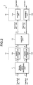
- FIG. 2 is a diagram illustrating an example configuration of a symbol mapping device according to a first embodiment of the present invention.
- a symbol mapping device 1 according to the first embodiment includes a transmission data processing unit 11, parity generation units 12A and 12B, a shuffle unit 13, and mapping units 14A and 14B.
- the parity generation units 12A and 12B together form a parity addition unit 12, and the mapping units 14A and 14B together form a mapping processing unit 14. Note that when a distinction is necessary between two consecutive TSs along the time axis, these TSs are referred to as a first TS and a second TS in the description given below.
- the symbol mapping device 1 illustrated in FIG. 2 adds parity data to each of data to be sent in the first TS, i.e., "Time Slot 0", and data to be sent in the second TS, i.e., "Time Slot 1", and then maps the resultant data to constellation points of a modulation scheme associated with the number of bits of the data to be sent in each TS.
- the transmission data processing unit 11 of the symbol mapping device 1 receives two pieces, i.e., two lines, of transmission data to be sent respectively using the first TS and the second TS. Specifically, as illustrated in FIG. 2 , transmission data b 0 , ..., and b 6 associated with "Time Slot 0" and transmission data b 0 , ..., and b 6 associated with "Time Slot 1" are input to the transmission data processing unit 11. Note that each line of transmission data has a length, i.e., the number of bits, equivalent to the number of bits to be sent per TS. That is, in a case in which the number of bits to be sent per TS is two bits, two bits per line, that is, a total of four bits, of transmission data are input to the transmission data processing unit 11.
- the transmission data processing unit 11 performs a transmission data length adjustment process, described later herein, on the two lines of transmission data input, and generates two lines of output data each having a length of a first length.
- the two lines of output data generated by the transmission data processing unit 11 are input data respectively input to the parity generation units 12A and 12B.
- the first length is herein assumed to be seven bits.
- the two lines of seven-it output data output from the transmission data processing unit 11 may each contain dummy data to adjust the length thereof to seven bits.
- FIG. 3 is a diagram illustrating an example configuration of the parity generation unit 12A, which is a first parity generation unit of the symbol mapping device 1 according to the first embodiment.
- the parity generation unit 12A includes bit extraction units 21A and 22A, and a look-up table circuit (LUT) 23A, which generates parity data.
- the parity generation unit 12A generates eight bits, i.e., a second length, of parity-added transmission data B 00 , ..., and B 07 , containing parity data added to the transmission data, on the basis of the seven bits of data b 00 , ..., and b 06 input from the transmission data processing unit 11.
- the bit extraction unit 21A i.e., a first bit extraction unit of the parity generation unit 12A, extracts the five most significant bits b 00 , ..., and b 04 from the seven bits of data input from the transmission data processing unit 11, and outputs the bits b 00 , ..., and b 04 to the shuffle unit 13 as bits B 00 , ..., and B 04 . That is, the bit extraction unit 21A is the first bit extraction unit that extracts a first number of bits of data from the output data of the transmission data processing unit 11, where the first number is less than the number of bits of the output data, and outputs the extracted data as part of the parity-added transmission data.
- the five bits of data output by the bit extraction unit 21A is part or all of the transmission data contained in the output data of the transmission data processing unit 11.
- the bit extraction unit 22A i.e., a second bit extraction unit of the parity generation unit 12A, extracts six bits from the seven bits of data input from the transmission data processing unit 11, and outputs these six bits to the LUT 23A. That is, the bit extraction unit 22A is the second bit extraction unit that extracts a second number of bits of data from the output data of the transmission data processing unit 11, where the second number is less than the number of bits of the output data. It is assumed herein that the six bits to be extracted from the seven bits of data by the bit extraction unit 22A is predetermined depending on the number of bits of data to be sent in one TS. Correspondence between the six bits to be extracted by the bit extraction unit 22A and the number of bits of data to be sent in one TS will be described later herein.
- the LUT 23A of the parity generation unit 12A generates parity data having a length up to three bits on the basis of the six bits of data input from the bit extraction unit 22A.
- the number of bits of the parity data generated by the LUT 23A differs depending on the number of bits of the transmission data per TS.
- the LUT 23A generates two bits of parity data in a case in which the transmission data has a length of two bits per TS, and generates one bit of parity data in a case in which the transmission data has a length of three bits per TS.
- the LUT 23A generates three bits of parity data in a case in which the transmission data has a length of five bits per TS, generates two bits of parity data in a case in which the transmission data has a length of six bits per TS, and generates one bit of parity data in a case in which the transmission data has a length of seven bits per TS.
- the remaining bit or bits other than the parity data, of the three bits of data output by the LUT 23A will be transmission data or dummy data.
- the three bits of data generated and output by the LUT 23A is the remaining three bits of the parity-added transmission data other than the five bits of the parity-added transmission data output by the bit extraction unit 21A described above, of a total of eight bits of the parity-added transmission data generated by the parity generation unit 12A.
- the parity data may be generated in any manner.
- the LUT 23A divides the six bits input into three groups each containing two bits, and performs an exclusive OR (XOR) operation on each pair of two bits to generate parity data.
- the LUT 23A performs an XOR operation on the most and second most significant bits, an XOR operation on the third and fourth most significant bits, and an XOR operation on the fifth and sixth most significant bits, of the six bits input, to obtain the three bits of parity data.
- the LUT 23A outputs the three bits of paty data generated, as bits B 05 , B 06 , and B 07 .
- the operations of the LUT 23A in the case in which the LUT 23A generates two bits of parity data and in the case in which the LUT 23A generates one bit of parity data will be described later herein. It is assumed herein that the configuration, i.e., the processing to be performed, of the LUT 23A is rewritable from outside the symbol mapping device 1.
- FIG. 4 is a diagram illustrating an example configuration of the parity generation unit 12B, which is a second parity generation unit of the symbol mapping device 1 according to the first embodiment.
- the parity generation unit 12B includes bit extraction units 21B and 22B, and a look-up table circuit (LUT) 23B, which generates parity data.
- the parity generation unit 12B generates eight bits of parity-added transmission data B 10 , ..., and B 17 , containing parity data added to the transmission data, on the basis of the seven bits of data b 10 , ..., and b 16 input from the transmission data processing unit 11.
- the bit extraction unit 21B i.e., a first bit extraction unit of the parity generation unit 12B, extracts the five most significant bits b 10 , ..., and b 14 from the seven bits of data input from the transmission data processing unit 11, and outputs the bits b 10 , ..., and b 14 to the shuffle unit 13 as bits B 10 , ..., and B 14 .
- the bit extraction unit 22B i.e., a second bit extraction unit of the parity generation unit 12B, extracts six bits from the seven bits input from the transmission data processing unit 11, and outputs these six bits to the LUT 23B.
- the bit extraction unit 22B operates similarly to the bit extraction unit 22A described above.
- the LUT 23B of the parity generation unit 12B generates parity data having a length up to three bits on the basis of the six bits of data input from the bit extraction unit 22B.
- the number of bits of the parity data generated by the LUT 23B differs depending on the number of bits of the transmission data per TS.
- the LUT 23B operates similarly to the LUT 23A described above. It is assumed herein that the configuration, i.e., the processing to be performed, of the LUT 23B is rewritable from outside the symbol mapping device 1.
- the shuffle unit 13 of the symbol mapping device 1 is a modulation data extraction unit.
- the shuffle unit 13 performs a shuffling process, described later, on the parity-added transmission data output from the parity generation unit 12A and on the parity-added transmission data output from the parity generation unit 12B, and extracts modulation data to be input to the mapping unit 14A and modulation data to be input to the mapping unit 14B.
- the mapping unit 14A which is a first mapping unit
- the mapping unit 14B which is a second mapping unit
- the phrase "valid bit contained in the modulation data” refers to a bit included in the transmission data or in the parity data.
- the modulation data contains four bits or eight bits of valid bits.
- the mapping unit 14A maps the modulation data to constellation points of the first TS
- the mapping unit 14B maps the modulation data to constellation points of the second TS.
- FIG. 5 is a diagram illustrating definitions of input signals to the transmission data processing unit 11 and of output signals of the transmission data processing unit 11.
- FIG. 6 is a diagram illustrating an example of the transmission data length adjustment process performed by the transmission data processing unit 11.
- the transmission data processing unit 11 receives two lines of transmission data b 00IN , ..., and b 06IN ; and b 10IN , ..., and b 16IN .
- the bits b 00IN , ..., and b 06IN respectively correspond to the bits b 0 , ..., and b 6 of TS0 (Time Slot 0) illustrated in FIG. 2
- the bits b 10IN , ..., and b 16IN respectively correspond to the bits b 0 , ..., and b 6 of TS1 (Time Slot 1) illustrated in FIG. 2
- the transmission data processing unit 11 outputs two lines of reproduced data B 00OUT , ..., and b 06OUT ; and b 10OUT , ..., and b 16OUT , which are results of performing of the transmission data length adjustment process.
- the transmission data processing unit 11 has three operation modes, and operates in a mode associated with the number of bits of data to be sent in one TS. It is assumed here that input data and output data per TS to and from the transmission data processing unit 11 have a bit width of seven bits. In a case in which the required number of bits is less than seven bits, that is, in a case in which the number of bits of data to be sent in one TS is less than seven bits, the transmission data processing unit 11 stores that data in the most significant bit positions.
- the remaining bit position(s) is or are filled with, for example, '0' or '0's, or given data as dummy data.
- FIG. 6 illustrates an example of filling the remaining bit position(s) with '0' or '0's as the dummy data.
- Mode 1 illustrated in FIG. 6 is an operation mode selected by the transmission data processing unit 11 in a case in which data having a length of five to seven bits is to be sent in one TS.
- the transmission data processing unit 11 outputs the bits b 00IN , ..., and b 06IN that have been input as the data to be sent in the first TS respectively as the bits B 00OUT , ..., and b 06OUT without change, and outputs the bits b 10IN , ..., and b 16IN that have been input as the data to be sent in the second TS respectively as the bits b 10OUT , ..., and b 16OUT without change.
- bits B 00OUT , ..., and b 06OUT , and the bits b 10OUT , ..., and b 16OUT respectively correspond to the bits b 00 , ..., and b 06 illustrated in FIG. 3 , and the bits b 10 , ..., and b 16 .
- Mode 2 illustrated in FIG. 6 is an operation mode selected by the transmission data processing unit 11 in a case in which data having a length of two bits is to be sent in one TS.
- the transmission data processing unit 11 outputs the bit b 00IN that has been input as data to be sent in the first TS, as the bits B 00OUT and b 10OUT , and outputs the bit b 01IN as the bits b 01OUT and b 11OUT .
- the transmission data processing unit 11 also outputs the bit b 10IN that has been input as data to be sent in the second TS, as the bits b 02OUT and b 12OUT , and also outputs the bit b 11IN as the bits b 03OUT and b 13OUT .
- the transmission data processing unit 11 further outputs '0's as the bits b 04OUT , ..., and b 06OUT , and as the bits b 14OUT , ..., and b 16OUT . That is, in Mode 2, the transmission data processing unit 11 combines together the input data to be sent in the first TS and the input data to be sent in the second TS, adds three bits of dummy data to the four bits of combined data, and then outputs the resultant data to the parity generation unit 12A and to the parity generation unit 12B.
- Mode 3 illustrated in FIG. 6 is an operation mode selected by the transmission data processing unit 11 in a case in which data having a length of three bits is to be sent in one TS.
- the transmission data processing unit 11 outputs the bit b 00IN that has been input as data to be sent in the first TS, as the bits B 00OUT and b 10OUT , outputs the bit b 01IN as the bits b 01OUT and b 11OUT , and outputs the bit b 02IN as the bits b 02OUT and b 12OUT .
- the transmission data processing unit 11 also outputs the bit b 10IN that has been input as data to be sent in the second TS, as the bits b 03OUT and b 13OUT , outputs the bit b 11IN as the bits b 04OUT and b 14OUT , and outputs the bit b 12IN as the bits b 05OUT and b 15OUT .
- the transmission data processing unit 11 further outputs '0's as the bits b 06OUT and b 16OUT .
- the transmission data processing unit 11 combines together the input data to be sent in the first TS and the input data to be sent in the second TS, add one bit of dummy data to the six bits of combined data, and then outputs the resultant data to the parity generation unit 12A and to the parity generation unit 12B.
- the transmission data processing unit 11 uses the two lines of transmission data input, as the two pieces of output data respectively to the two parity generation units 12A and 12B.
- the transmission data processing unit 11 adds dummy data to the two lines of transmission data input, to generate two pieces of first-length data, and uses these two pieces of first-length data as the two pieces of output data respectively to the two parity generation units 12A and 12B.
- the transmission data processing unit 11 combines together the two lines of transmission data, and adds the dummy data thereto to adjust the length to the first length.
- FIG. 7 is a diagram illustrating definitions of input signals to the shuffle unit 13 and of output signals of the shuffle unit 13.
- FIG. 8 is a diagram illustrating an example of shuffling process performed by the shuffle unit 13.
- the shuffle unit 13 receives a total of 16 bits of parity-added transmission data B 00IN , ..., and B 07IN , and B 10IN , ..., and B 17IN from the parity generation units 12A and 12B.
- the bits B 00IN , ..., and B 07IN , and the bits B 10IN , ..., and B 17IN respectively correspond to the bits B 00 , ..., and B 07 illustrated in FIG. 3 , and the bits B 10 , ..., and B 17 .
- the shuffle unit 13 also has three operation modes, and operates in a mode associated with the number of bits of data to be sent in one TS. It is assumed here that input data and output data per TS to and from the shuffle unit 13 have a bit width of eight bits. In a case in which the required number of bits is less than eight bits, that is, in a case in which the number of bits of data to be sent in one TS is less than eight bits, the shuffle unit 13 stores the modulation data in the most significant bit positions. The remaining bit position(s) is or are filled with, for example, '0' or '0's, or given data as dummy data. FIG. 8 illustrates an example of filling the remaining bit positions with '0's as the dummy data.
- Mode 1 illustrated in FIG. 8 is an operation mode selected by the shuffle unit 13 in a case in which data having a length of five to seven bits is to be sent in one TS.
- the shuffle unit 13 outputs the input bits B 00IN , ..., and B 07IN respectively as the modulation data B 00OUT , ..., and B 07OUT without change, and outputs the input bits B 10IN , ..., and B 17IN respectively as the modulation data B 10OUT , ..., and B 17OUT without change.
- the bits B 00OUT , ..., and B 07OUT output by the shuffle unit 13 are mapped to constellation points by the mapping unit 14A
- the bits B 10OUT , ..., and B 17OUT are mapped to constellation points by the mapping unit 14B.
- the bits B 00OUT , ..., and B 0VOUT respectively correspond to the bits B 0 , ..., and B 7 of TS0 (Time Slot 0) illustrated in FIG. 2
- the bits B 10OUT , ..., and B 17OUT respectively correspond to the bits B 0 , ..., and B 7 of TS1 (Time Slot 1) illustrated in FIG. 2 .
- Mode 2 illustrated in FIG. 8 is an operation mode selected by the shuffle unit 13 in a case in which data having a length of two bits is to be sent in one TS.
- the shuffle unit 13 outputs the input bits B 00IN , ..., and B 03IN respectively as the bits B 00OUT , ..., and B 03OUT ; outputs the input bits B 05IN , B 06IN , B 15IN , and B 16IN respectively as the bits B 10OUT , ..., and B 13OUT ; and outputs '0's as the bits B 04OUT , ..., and B 07OUT and as the bits B 14OUT , ..., and B 17OUT .
- bits B 00OUT , ..., and B 03OUT output by the shuffle unit 13 are mapped to constellation points by the mapping unit 14A, and the bits B 10OUT , ..., and B 13OUT are mapped to constellation points by the mapping unit 14B.
- Mode 3 illustrated in FIG. 8 is an operation mode selected by the shuffle unit 13 in a case in which data having a length of three bits is to be sent in one TS.
- the shuffle unit 13 outputs the input bits B 00IN , ..., and B 03IN respectively as the bits B 00OUT , ..., and B 03OUT , outputs the input bits B 04IN , B 05IN , B 06IN , and B 16IN respectively as the bits B 10OUT , ..., and B 13OUT , and outputs '0's as the bits B 04OUT , ..., and B 07OUT and as the bits B 14OUT , ..., and B 17OUT .
- bits B 00OUT , ..., and B 03OUT output by the shuffle unit 13 are mapped to constellation points by the mapping unit 14A, and the bits B 10OUT , ..., and B 13OUT are mapped to constellation points by the mapping unit 14B.
- the shuffle unit 13 extracts two pieces of modulation data, which are data to be mapped, from the two pieces of parity-added transmission data respectively generated by the two parity generation units 12A and 12B.
- a symbol mapping operation performed by the symbol mapping device 1 according to the first embodiment will next be described.
- the transmission data processing unit 11 and the shuffle unit 13 of the symbol mapping device 1 each operate in a mode associated with the number of bits of the transmission data per TS. Accordingly, the operation of the symbol mapping device 1 will be described below individually according to the number of bits of the transmission data per TS.
- the LUTs 23A and 23B included in the respective parity generation units 12A and 12B of the symbol mapping device 1 each have an internal configuration rewritten in advance on the basis of the number of bits of the transmission data per TS.
- the transmission data that are input in two lines will hereinafter be described such that one line of data is referred to as odd-numbered line of data and the other line of data is referred to as even-numbered line of data.
- the transmission data processing unit 11 selects and operates in Mode 2 illustrated in FIG. 6 .
- the transmission data processing unit 11 combines together the two bits of data of the odd-numbered line input and the two bits of data of the even-numbered line input to generate four bits of data.
- the transmission data processing unit 11 then outputs the four bits of data generated, as odd-numbered and even-numbered lines of data. That is, the transmission data processing unit 11 outputs the same data to both the parity generation units 12A and 12B. This allows the parity generation units 12A and 12B to each calculate the parity data from the two TSs of transmission data.
- the bit extraction unit 22A of the parity generation unit 12A extracts, for example, the six most significant bits of data from input data containing a total of four bits of transmission data for two TSs respectively corresponding to the odd-numbered and even-numbered lines, and then outputs these six bits of data to the LUT 23A.
- the LUT 23A generates two bits of data, of the total of four bits of parity data for two TSs, on the basis of the six bits of data input, and then outputs these two bits of data.
- the bit extraction unit 22B of the parity generation unit 12B extracts, for example, the six most significant bits of data from input data containing a total of four bits of transmission data for two TSs respectively corresponding to the odd-numbered and even-numbered lines, and then outputs these six bits of data to the LUT 23B.
- the LUT 23B generates two bits of data, of the four bits of parity data for two TSs, on the basis of the six bits of data input. That is, the parity generation units 12A and 12B together generate a total of four bits of parity data for two TSs.
- the fifth and sixth bits of the data input to each of the parity generation units 12A and 12B are dummy data, and therefore, the LUT 23A and the LUT 23B are each configured such that the output thereof does not depend on the fifth and sixth bits of the input data. That is, the LUT 23A and the LUT 23B are each configured not to use the fifth and sixth bits of the input data in the process of generating the two bits of parity data.
- the LUT 23A When the parity generation units 12A and 12B generate a total of four bits of parity data for two TSs, the LUT 23A generates, for example, the two most significant bits of the parity data, and the LUT 23A outputs these two bits of data generated, as the two most significant bits of the three-bit output. In addition, the LUT 23B generates the two least significant bits of the parity data, and the LUT 23B outputs these two bits of data generated, as the two most significant bits of the three-bit output. The remaining one bit of the output of each of the LUTs 23A and 23B is dummy data.
- the four most significant bits (B 00 , ..., and B 03 ; and B 10 , ..., and B 13 ) of the output of each of the parity generation units 12A and 12B are used to output the transmission data
- the sixth and seventh bits (B 05 , B 06 ) of the output of the parity generation unit 12A and the sixth and seventh bits (B 15 , B 16 ) of the output of the parity generation unit 12B together constitute the parity data.
- the shuffle unit 13 rearranges the four most significant bits (B 00 , ..., and B 03 ) and the sixth and seventh bits (B 05 , B 06 ) of the output of the parity generation unit 12A, and the sixth and seventh bits (B 15 , B 16 ) of the output of the parity generation unit 12B according to the rule of Mode 2 illustrated in FIG. 8 , and then outputs the resultant data as the modulation data. Selection of Mode 2 and operation in Mode 2 allow the shuffle unit 13 to generate four bits of modulation data per TS using the transmission data and the parity data output from the parity generation units 12A and 12B.
- the mapping units 14A and 14B each map the modulation data input from the shuffle unit 13 to, for example, quadrature phase shift keying (QPSK) constellation points illustrated in FIG. 9 , and then outputs coordinate sets of the respective constellation points.
- QPSK quadrature phase shift keying
- the mapping unit 14A maps the two most significant bits B 0 and B 1 to the X-polarized wave of the first TS, and maps the two least significant bits B 2 and B 3 to the Y-polarized wave.
- the mapping unit 14B maps the two most significant bits B 0 and B 1 to the X-polarized wave of the second TS, and maps the two least significant bits B 2 and B 3 to the Y-polarized wave.
- the symbol mapping device 1 assigns the total of four bits of transmission data input to the transmission data processing unit 11 to the first TS, and assigns the total of four bits of parity data generated by the parity generation units 12A and 12B to the second TS.
- the arrangement in assigning the four bits of transmission data and the four bits of parity data depends on the specification of the shuffle unit 13, but the manner of the bit assignment is not limited to the arrangement described above.
- the shuffle unit 13 may be configured to assign two bits of transmission data and two bits of parity data to each of the first TS and the second TS.
- the transmission data processing unit 11 selects and operates in Mode 3 illustrated in FIG. 6 .
- the transmission data processing unit 11 combines together the three bits of data of the odd-numbered line input and the three bits of data of the even-numbered line input to generate six bits of data.
- the transmission data processing unit 11 then outputs the six bits of data generated, as odd-numbered and even-numbered lines of data. That is, the transmission data processing unit 11 outputs the same data to both the parity generation units 12A and 12B. This allows the parity generation units 12A and 12B to calculate the parity data from the two TSs of transmission data.
- the bit extraction unit 22A of the parity generation unit 12A extracts the six most significant bits of data, which will be six bits of the transmission data for one TS of the odd-numbered line, from the seven-bit input data, and then outputs these six bits of data to the LUT 23A.
- the LUT 23A generates one bit of data, of the two bits of parity data for two TSs, on the basis of the six bits of data input, and then outputs this one bit of data.
- the bit extraction unit 22B of the parity generation unit 12B extracts the six most significant bits of data, which will be six bits of the transmission data for one TS of the even-numbered line, from the seven-bit input data, and then outputs these six bits of data to the LUT 23B.
- the LUT 23B generates one bit of data, of the two bits of parity data for two TSs, on the basis of the six bits of data input, and then outputs this one bit of data.
- extraction of the five most significant bits of the transmission data from the seven-bit input data by the bit extraction unit 21A in the parity generation unit 12A requires the parity generation unit 12A to output the sixth bit of the transmission data through the bit extraction unit 22A and the LUT 23A.
- extraction of the five most significant bits of the transmission data from the seven-bit input data by the bit extraction unit 21B in the parity generation unit 12B requires the parity generation unit 12B to output the sixth bit of the transmission data through the bit extraction unit 22B and the LUT 23B.
- the LUT 23A outputs the sixth bit of the transmission data as the most significant bit of the three-bit output, generates the most significant bit of the parity data, and outputs this most significant bit of the parity data as the second bit of the three-bit output.
- the LUT 23B outputs the sixth bit of the transmission data as the most significant bit of the three-bit output, generates the least significant bit of the parity data, and outputs this least significant bit of the parity data as the second bit of the three-bit output.
- the third bit of the output of the LUT 23A and the third bit of the output of the LUT 23B are dummy data.
- the six most significant bits (B 00 , ..., and B 05 ; and B 10 , ..., and B 15 ) of the output of each of the parity generation units 12A and 12B are used to output the transmission data, and the seventh bit (B 06 ) of the output of the parity generation unit 12A and the seventh bit (B 16 ) of the output of the parity generation unit 12B together constitute the parity data.
- the shuffle unit 13 rearranges the six most significant bits (B 00 , ..., and B 05 ) of the output of the parity generation unit 12A and the seventh bit (B 16 ) of the output of the parity generation unit 12B according to the rule of Mode 3 illustrated in FIG. 8 , and then outputs the resultant data as the modulation data. Selection of Mode 3 and operation in Mode 3 allow the shuffle unit 13 to generate four bits of modulation data per TS using the transmission data and the parity data output from the parity generation units 12A and 12B.
- the mapping units 14A and 14B each map the modulation data input from the shuffle unit 13 to, for example, QPSK constellation points illustrated in FIG. 9 , and then outputs coordinate sets of the respective constellation points.
- the symbol mapping device 1 assigns four bits of the total of six bits of transmission data input to the transmission data processing unit 11 to the first TS, and assigns the remaining two bits of the transmission data and the total of two bits of parity data generated by the parity generation units 12A and 12B to the second TS.
- the manner of the bit assignment is not limited to the arrangement described above.
- the shuffle unit 13 may be configured to assign three bits of transmission data and one bit of parity data to each of the first TS and the second TS.
- the transmission data processing unit 11 selects and operates in Mode 1 illustrated in FIG. 6 . In this case, the transmission data processing unit 11 outputs, without change, the five bits of data of the odd-numbered line input and the five bits of data of the even-numbered line input. In this operation, the transmission data processing unit 11 outputs dummy data as the sixth and seventh bits of the data of each of the odd-numbered and even-numbered lines. The transmission data processing unit 11 outputs, for example, '0's as the dummy data.
- the bit extraction unit 22A of the parity generation unit 12A extracts, for example, the six most significant bits of data from the seven-bit input data, and then outputs these six bits of data to the LUT 23A.
- the LUT 23A outputs three bits of parity data for one TS on the basis of the six bits of data input.
- the bit extraction unit 22B of the parity generation unit 12B extract, for example, the six most significant bits of data from the seven-bit input data, and then outputs these six bits of data to the LUT 23B.
- the LUT 23B outputs three bits of parity data for one TS on the basis of the six bits of data input.
- the sixth bit of the data input to each of the parity generation units 12A and 12B is dummy data, and therefore, the LUT 23A and the LUT 23B are each configured such that the output thereof does not depend on the sixth bit of the input data. That is, the LUT 23A and the LUT 23B are each configured not to use the sixth bit of the input data in the process of generating the three bits of parity data.
- the shuffle unit 13 outputs, without change, the eight bits (B 00 , ..., and B 07 ) of the output of the parity generation unit 12A and the eight bits (B 10 , ..., and B 17 ) of the output of the parity generation unit 12B according to the rule of Mode 1 illustrated in FIG. 8 .
- the mapping units 14A and 14B each map the modulation data input from the shuffle unit 13 to, for example, 16-QAM constellation points illustrated in FIG. 10 or 2A8PSK constellation points illustrated in FIG. 11 , and then outputs coordinate sets of the respective constellation points.
- the mapping unit 14A maps the four most significant bits B 0 , ..., and B 3 to the X-polarized wave of the first TS, and maps the four least significant bits B 4 , ..., and B 7 to the Y-polarized wave.
- the mapping unit 14B maps the four most significant bits B 0 , ..., and B 3 to the X-polarized wave of the second TS, and maps the four least significant bits B 4 , ..., and B 7 to the Y-polarized wave.
- the transmission data processing unit 11 selects and operates in Mode 1 illustrated in FIG. 6 .
- the transmission data processing unit 11 outputs, without change, the six bits of data of the odd-numbered line input and the six bits of data of the even-numbered line input.
- the transmission data processing unit 11 outputs dummy data as the seventh bit of the data of each of the odd-numbered and even-numbered lines.
- the transmission data processing unit 11 outputs, for example, '0' as the dummy data.
- the bit extraction unit 22A of the parity generation unit 12A extracts the six most significant bits of data, which will be the transmission data for one TS of the odd-numbered line, from the seven-bit input data, and then outputs these six bits of data to the LUT 23A.
- the LUT 23A generates two bits of parity data for one TS on the basis of the six bits of data input, and then outputs these two bits of data.
- the bit extraction unit 22B of the parity generation unit 12B extracts the six most significant bits of data, which will be the transmission data for one TS of the even-numbered line, from the seven-bit input data, and then outputs these six bits of data to the LUT 23B.
- the LUT 23B generates two bits of parity data for one TS on the basis of the six bits of data input, and then outputs these two bits of data.
- extraction of the five most significant bits of the transmission data from the seven-bit input data by the bit extraction unit 21A in the parity generation unit 12A requires the parity generation unit 12A to output the sixth bit of the transmission data through the bit extraction unit 22A and the LUT 23A.
- extraction of the five most significant bits of the transmission data from the seven-bit input data by the bit extraction unit 21B in the parity generation unit 12B requires the parity generation unit 12B to output the sixth bit of the transmission data through the bit extraction unit 22B and the LUT 23B.
- the LUT 23A outputs the sixth bit of the transmission data as the most significant bit of the three-bit output, and outputs the parity data using the remaining two bits of the three-bit output.
- the LUT 23B outputs the sixth bit of the transmission data as the most significant bit of the three-bit output, and outputs the parity data using the remaining two bits of the three-bit output.
- the shuffle unit 13 outputs, without change, the eight bits (B 00 , ..., and B 07 ) of the output of the parity generation unit 12A and the eight bits (B 10 , ..., and B 17 ) of the output of the parity generation unit 12B according to the rule of Mode 1 illustrated in FIG. 8 .
- the mapping units 14A and 14B maps the modulation data input from the shuffle unit 13 to, for example, 16-QAM constellation points illustrated in FIG. 10 or 2A8PSK constellation points illustrated in FIG. 11 , and then outputs coordinate sets of the respective constellation points.
- the transmission data processing unit 11 selects and operates in Mode 1 illustrated in FIG. 6 . In this case, the transmission data processing unit 11 outputs, without change, the seven bits of data of the odd-numbered line input and the seven bits of data of the even-numbered line input.
- the bit extraction unit 22A of the parity generation unit 12A extracts, for example, the six least significant bits of data from the seven-bit input data, and then outputs these six bits of data to the LUT 23A.
- the LUT 23A outputs one bit of parity data for one TS on the basis of the six bits of data input.
- the bit extraction unit 22B of the parity generation unit 12B extracts, for example, the six least significant bits of data from the seven-bit input data, and then outputs these six bits of data to the LUT 23B.
- the LUT 23B outputs one bit of parity data for one TS on the basis of the six bits of data input.
- extraction of the five most significant bits of the transmission data from the seven-bit input data by the bit extraction unit 21A in the parity generation unit 12A requires the parity generation unit 12A to output the sixth and seventh bits of the transmission data through the bit extraction unit 22A and the LUT 23A.
- extraction of the five most significant bits of the transmission data from the seven-bit input data by the bit extraction unit 21B in the parity generation unit 12B requires the parity generation unit 12B to output the sixth and seventh bits of the transmission data through the bit extraction unit 22B and the LUT 23B.
- the LUT 23A outputs the sixth and seventh bits of the transmission data using the two most significant bits of the three-bit output, and outputs the parity data using the remaining one bit of the three-bit output.
- the LUT 23B outputs the sixth and seventh bits of the transmission data using the two most significant bits of the three-bit output, and outputs the parity data using the remaining one bit of the three-bit output.
- the shuffle unit 13 outputs, without change, the eight bits (B 00 , ..., and B 07 ) of the output of the parity generation unit 12A and the eight bits (B 10 , ..., and B 17 ) of the output of the parity generation unit 12B according to the rule of Mode 1 illustrated in FIG. 8 .
- the mapping units 14A and 14B each map the modulation data input from the shuffle unit 13 to, for example, 16-QAM constellation points illustrated in FIG. 10 or 2A8PSK constellation points illustrated in FIG. 11 , and then outputs coordinate sets of the respective constellation points.
- the symbol mapping device 1 includes the parity generation units 12A and 12B, and the parity generation units 12A and 12B each generate parity data having a size associated with the number of bits of the transmission data per TS using a six-bit input and three-bit output LUT.
- the symbol mapping device 1 also includes the transmission data processing 11 that adjusts the number of bits of the transmission data to be input to each of the parity generation units 12A and 12B to enable the parity generation units 12A and 12B to each use the six-bit input and three-bit output LUT.
- This configuration provides a symbol mapping device having a set of variable parity generation rules, thereby enabling a reduction in the LUT size.
- the symbol mapping device 1 is implemented by, for example, an ASIC
- a reduction in the LUT size can reduce the circuit size of the ASIC because the LUT will be the main circuit of the ASIC.
- FIG. 12 is a diagram illustrating an example configuration of a symbol mapping device according to a second embodiment.
- a symbol mapping device 1a according to the second embodiment is configured such that the parity generation units 12A and 12B of the symbol mapping device 1 described in the first embodiment are replaced by parity generation units 32A and 32B and that the shuffle unit 13 is replaced by a shuffle unit 33.
- the parity generation units 32A and 32B together form a parity addition unit 32.
- the present embodiment describes the parity generation units 32A and 32B and the shuffle unit 33 different from the corresponding components of the first embodiment, and a description of the other components will be omitted.
- FIG. 13 is a diagram illustrating an example configuration of the parity generation unit 32A, which is a first parity generation unit of the symbol mapping device 1a according to the second embodiment.
- the parity generation unit 32A according to the second embodiment includes the bit extraction units 21A and 22A and an LUT 43A.
- the parity generation unit 32A differs from the parity generation unit 12A described in the first embodiment in including the LUT 43A, and the other components are the same.
- FIG. 14 is a diagram illustrating an example configuration of the parity generation unit 32B, which is a second parity generation unit of the symbol mapping device 1a according to the second embodiment.
- the parity generation unit 32B according to the second embodiment includes the bit extraction units 21B and 22B and an LUT 43B.
- the parity generation unit 32B differs from the parity generation unit 12B described in the first embodiment in including the LUT 43B, and the other components are the same.
- the LUTs 23A and 23B described in the first embodiment are each configured to output three bits from a six-bit input.
- the LUTs 43A and 43B according to the present embodiment differ from the LUTs 23A and 23B in that they are configured to output two bits from a six-bit input.
- the parity generation units 32A and 32B each output seven bits of parity-added transmission data. Specifically, the parity generation units 32A and 32B each generate and output the seven most significant bits that result from discarding the least significant bit from the eight bits of the data output by the parity generation units 12A and 12B described in the first embodiment.
- the parity generation units 32A and 32B each generate the seven-bit output data similarly to the parity generation units 12A and 12B that generate the seven most significant bits of the output data. It is assumed herein that the configuration, i.e., the processing to be performed, of each of the LUTs 43A and 43B is rewritable from outside the symbol mapping device 1a.
- the shuffle unit 33 generates a total of 16 bits of modulation data on the basis of a total of 14 bits of parity-added transmission data input from the LUTs 43A and 43B.
- FIG. 15 is a diagram illustrating definitions of input signals to the shuffle unit 33 and of output signals of the shuffle unit 33.
- FIG. 16 is a diagram illustrating an example of shuffling process performed by the shuffle unit 33.
- Mode 1 is an operation mode selected by the shuffle unit 33 in a case in which data having a length of five to seven bits is to be sent in one TS.
- Mode 2 is an operation mode selected by the shuffle unit 33 in a case in which data having a length of two bits is to be sent in one TS.
- Mode 3 is an operation mode selected by the shuffle unit 33 in a case in which data having a length of three bits is to be sent in one TS.
- the shuffle unit 33 receives parity-added transmission data B 00IN , ..., and B 06IN , and B 10IN , ..., and B 16IN from the parity generation units 32A and 32B.
- the bits B 00IN , ..., and B 06IN respectively correspond to the bits B 00 , ..., and B 06 illustrated in FIG. 13
- the bits B 10IN , ..., and B 16IN respectively correspond to the bits B 10 , ..., and B 16 illustrated in FIG. 14 .
- the shuffle unit 33 outputs the same data as the data output by the shuffle unit 13 described in the first embodiment in Mode 2 and in Mode 3.
- the symbol ' ⁇ ' represents logical inversion.
- bits B 00OUT , ..., and B 07OUT illustrated in FIG. 15 respectively correspond to the bits B 0 , ..., and B 7 of TS0 (Time Slot 0) illustrated in FIG. 12
- bits B 10OUT , ..., and B 17OUT illustrated in FIG. 15 respectively correspond to the bits B 0 , ..., and B 7 of TS1 (Time Slot 1) illustrated in FIG. 12 .
- the shuffle unit 33 also has three operation modes, and operates in a mode associated with the number of bits of data to be sent in one TS. It is assumed here that the input data per TS to the shuffle unit 33 has a bit width of seven bits and the output data per TS has a bit width of eight bits. In a case in which the number of bits of data to be sent in one TS is less than eight bits, the shuffle unit 33 stores the modulation data in the most significant bit positions. The remaining bit position(s) is or are filled with, for example, '0' or '0's, or given data as the dummy data.
- a symbol mapping operation performed by the symbol mapping device 1a according to the second embodiment will next be described. Similarly to the first embodiment, the operation of the symbol mapping device 1a will be described below individually according to the number of bits of the data to be sent per TS.
- the symbol mapping device 1a operates differently from the symbol mapping device 1 described in the first embodiment that sends two bits or three bits of data per TS, in not outputting the dummy data in the least significant bit position of the data input from each of the parity generation units 32A and 32B to the shuffle unit 33.
- Other operations of the symbol mapping device 1a are the same as those of the symbol mapping device 1.
- the LUTs 23A and 23B of the respective parity generation units 12A and 12B described in the first embodiment each output dummy data in the third bit position of the three-bit output, while the LUTs 43A and 43B of the respective parity generation units 32A and 32B do not output the dummy data in the third bit position described above.
- the LUTs 43A and 43B in the symbol mapping device 1a each output two bits of parity data on the basis of the six bits of data input.
- the sixth bit of the data input to each of the LUTs 43A and 43B is dummy data, and therefore, the LUT 43A and the LUT 43B are each configured such that the output thereof does not depend on the sixth bit of the input data.
- Sending of five-bit data per TS requires three bits of parity data per TS, but the parity generation units 32A and 32B each output only two bits of parity data.
- the shuffle unit 33 outputs parity data generated by logical inversion of the seventh bit of the data input, as the eighth bit of the modulation data as illustrated in FIGs. 15 and 16 .
- the LUTs 43A and 43B in the symbol mapping device 1a each output one bit of parity data on the basis of the six bits of data input. That is, the LUTs 43A and 43B each output the sixth bit of the transmission data using the first bit of the two-bit output, and output the parity data using the second bit of the two-bit output.
- Sending of six-bit data per TS requires two bits of parity data per TS, but the parity generation units 32A and 32B each output only one bit of parity data.
- the shuffle unit 33 outputs parity data generated by logical inversion of the seventh bit of the data input, as the eighth bit of the modulation data as illustrated in FIGs. 15 and 16 .
- the LUTs 43A and 43B in the symbol mapping device 1a each output the sixth bit of the transmission data using the first bit of the two-bit output, and output the seventh bit of the transmission data using the second bit of the two-bit output.
- Sending of seven-bit data per TS requires one bit of parity data per TS, but no parity data is output from the parity generation units 32A and 32B.
- the shuffle unit 33 outputs parity data generated by logical inversion of the seventh bit of the data input, as the eighth bit of the modulation data as illustrated in FIGs. 15 and 16 .
- the symbol mapping device 1a includes the parity generation units 32A and 32B, and the parity generation units 32A and 32B each generate parity data having a length up to two bits depending on the number of bits of the transmission data per TS, using a six-bit input and two-bit output LUT.
- the shuffle unit 33 generates the parity data and adds the parity data to the transmission data. This can further reduce the circuit size of an LUT as compared to the circuit size thereof in the first embodiment.
- the transmission data processing unit, the parity generation units, the shuffle unit, and the mapping units included in the symbol mapping devices 1 and 1a are implemented in a processing circuit. That is, the symbol mapping devices 1 and 1a each include a processing circuit for converting transmission data to constellation point coordinate sets.
- the processing circuit may be a dedicated hardware element, or may be a control circuit including a processor and a memory.
- FIG. 17 is a diagram illustrating an example configuration of hardware in a case in which components of each of the symbol mapping devices 1 and 1a are implemented in a dedicated hardware element.
- a processing circuit 101 which is the dedicated hardware element, is, for example, a single circuit, a composite circuit, a programmed processor, a parallel programmed processor, an ASIC, a field programmable gate array (FPGA), or a combination thereof.
- the transmission data processing unit, the parity generation units, the shuffle unit, and the mapping units may be implemented in a combination of multiple processing circuits, or the functionality of these components may be collectively implemented in a single processing circuit.
- FIG. 18 is a diagram illustrating an example configuration of hardware in a case in which components of each of the symbol mapping devices 1 and 1a are implemented in a control circuit.
- the control circuit includes a processor 201 and a memory 202.
- the processor 201 is a central processing unit (CPU) (also referred to as central processing unit, processing circuit, computing unit, microprocessor, microcomputer, or digital signal processor (DSP)), a system large scale integration (LSI), or the like.
- CPU central processing unit
- DSP digital signal processor
- LSI system large scale integration
- the memory 202 is generally a non-volatile or volatile semiconductor memory such as a random access memory (RAM), a read-only memory (ROM), a flash memory, an erasable programmable read-only memory (EPROM), or an electrically erasable programmable read-only memory (EEPROM), but may also be a magnetic disk, a flexible disk, an optical disk, a compact disc, a MiniDisc, a digital versatile disc (DVD), or the like.
- RAM random access memory
- ROM read-only memory
- EPROM erasable programmable read-only memory
- EEPROM electrically erasable programmable read-only memory
- the transmission data processing unit, the parity generation units, the shuffle unit, and the mapping units of each of the symbol mapping devices 1 and 1a are implemented in a control circuit
- the functionality of these components is implemented in software, firmware, or a combination of software and firmware.
- the software or firmware is described as a program, and is stored in the memory 202.
- the processor 201 reads and executes a program stored in the memory 202 to implement the functionality of the components of the symbol mapping devices 1 and 1a.
- the symbol mapping devices 1 and 1a each include the memory 202 for storing a program that, upon execution by the control circuit, causes the step of adjusting the transmission data length, the step of generating parity data, the step of rearranging the bits of the modulation data, and the step of assigning the modulation data to constellation point coordinate sets, to be performed. It can also be said that this program causes a computer to perform methods or procedures of the transmission data processing unit, the parity generation units, the shuffle unit, and the mapping units.
- the transmission data processing unit, the parity generation units, the shuffle unit, and the mapping units may be implemented partially in a dedicated hardware element, and partially in software or firmware.
- a configuration may be used in which the functionality of the parity generation units is implemented in a processing circuit serving as a dedicated hardware element, while the functionality of the transmission data processing unit, the shuffle unit, and the mapping units is implemented in a processor that reads and executes a program stored in a memory.
- implementation of the parity generation units in a dedicated hardware element can reduce the circuit size.
- implementation of the parity generation units in software or firmware can reduce the processing load.
- the processing circuit enables the functionality of the symbol mapping devices 1 and 1a to be implemented in hardware, software, firmware, or a combination thereof.
- 1, 1a symbol mapping device 11 transmission data processing unit; 12, 32 parity addition unit; 12A, 12B, 32A, 32B parity generation unit; 13, 33 shuffle unit; 14 mapping processing unit; 14A, 14B mapping unit; 21A, 21B, 22A, 22B bit extraction unit; 23A, 23B, 43A, 43B look-up table (LUT).
Landscapes
- Engineering & Computer Science (AREA)
- Computer Networks & Wireless Communication (AREA)
- Signal Processing (AREA)
- Physics & Mathematics (AREA)
- Probability & Statistics with Applications (AREA)
- Theoretical Computer Science (AREA)
- Quality & Reliability (AREA)
- Error Detection And Correction (AREA)
- Digital Transmission Methods That Use Modulated Carrier Waves (AREA)
Abstract
Description
- The present invention relates to a symbol mapping device applicable to an optical communication system.
- To implement an optimum modulation scheme for system requirements in an optical communication system, multi-dimensional modulation techniques have been proposed which allow a spectral efficiency to be selected with a finer granularity, in addition to conventional dual polarization quadrature amplitude modulation (QAM) techniques. A conventional dual polarization QAM maps transmission data to a constellation point independently in a two-dimensional space of each of the polarized waves. In contrast, multi-dimensional modulation maps transmission data to a constellation point in a four- or higher-dimensional space formed of two polarized waves and of multiple time slots (TSs). Thus, multi-dimensional modulation can use an increased Euclidean distance between constellation points, and thus can increase noise tolerance. Multi-dimensional modulation can also increase nonlinearity tolerance by reducing signal power variations in each TS and/or increasing the level of randomness in a polarized state (see Non-Patent Literature 1). Note that mapping over n TSs is performed such that data is mapped to constellation points in a 4n-dimensional space.
- Typically, in symbol mapping in multi-dimensional modulation, parity data is added to the transmission data, which is then rearranged to form data to be modulated (hereinafter referred to simply as "modulation data"), and the modulation data is mapped to constellation points of a QAM scheme or to constellation points of a 2-ary amplitude 8-ary phase shift keying (2A8PSK) scheme. Transmission data is converted to modulation data using a circuit including a look-up table (LUT) or the like or using a dedicated symbol mapping circuit applicable only to a specific multi-dimensional modulation scheme (see Patent Literature 1).
- Patent Literature 1: European Patent Application Publication No.
2506458 - Non-Patent Literature 1: K. Kojima, et al., "Constant modulus 4D optimized constellation alternative for DP-8QAM", Proc. ECOC, P. 3.25 (2014).
- In a circuit configuration that uses an LUT to convert transmission data into modulation data, use of a rewritable LUT enables multiple types of multi-dimensional modulations that each provide a different spectral efficiency to be implemented in one application specific integrated circuit (ASIC). However, the configuration using a rewritable LUT raises a problem in that the circuit size increases.
- By way of example, consider a circuit that converts transmission data into modulation data using an LUT is capable of performing multi-dimensional modulation on any transmission data that is two-bit, three-bit, five-bit, six-bit, or seven-bit transmission data. In this case, input and output of the LUT may or may not use as many as two TSs. The case in which input and output of the LUT use as many as two TSs is a case in which two TSs of transmission data are together input to the LUT and two TSs of transmission data, generated by addition of parity data, is then output. This is the case for transmission data having a length of two bits or three bits. The case in which input and output of the LUT do not use as many as two TSs is a case in which one TS of transmission data is input to the LUT and one TS of transmission data, generated by addition of parity data, is then output. This is the case for transmission data having a length of five bits or more. The possibility that input and output of the LUT may or may not use as many as two TSs requires two types of LUTs to support both cases. Specifically, in a case in which input and output use as many as two TSs, one six-bit input and eight-bit output LUT is required per two TSs; and in a case in which input and output do not use as many as two TSs, one seven-bit input and eight-bit output LUT is required for each of two TSs. That is, a total of three LUTs are required, thereby increasing the circuit size.
- Note that if transmission data that is input to each LUT has a bit width less than the input bit width of the corresponding LUT, the transmission data as well as dummy data are input to each LUT. For example, when two-bit transmission data is input to a six-bit input and eight-bit output LUT for each of two TSs, a total of four bits of transmission data for two TSs and two bits of dummy data are input to the LUT, and the LUT generates four bits of parity data on the basis of the four bits of transmission data.
- The present invention has been made in view of the foregoing, and it is an object of the present invention to provide a symbol mapping device that provides multiple types of multi-dimensional modulations each providing a different spectral efficiency and is also capable of reducing the size of the circuit.
- To solve the problem and achieve the object described above, a symbol mapping device according to an aspect of the present invention includes: a transmission data processing unit to receive two pieces of transmission data having a same length, and in a case in which the length is a first length, to use the two pieces of transmission data as two pieces of output data without change, and in a case in which the length is less than the first length, to add dummy data to the two pieces of transmission data to generate two pieces of output data, each piece having the first length; and a parity addition unit to generate two pieces of parity-added transmission data on a basis of the two pieces of output data, the two pieces of parity-added transmission data each containing parity data added to the transmission data and each having a second length. The symbol mapping device further includes: a modulation data extraction unit to extract two pieces of modulation data, being data to be mapped, from the two pieces of parity-added transmission data generated by the parity addition unit; and a mapping processing unit to map the two pieces of modulation data to two time slots of constellation points.
- According to the present invention, an advantage is provided in that a symbol mapping device can be provided that provides multiple types of multi-dimensional modulations each providing a different spectral efficiency and is also capable of reducing the size of the circuit.
-
-
FIG. 1 is a diagram illustrating an example specification for implementing multiple types of multi-dimensional modulations each providing a different spectral efficiency using a look-up table. -
FIG. 2 is a diagram illustrating an example configuration of a symbol mapping device according to a first embodiment. -
FIG. 3 is a diagram illustrating an example configuration of a first parity generation unit according to the first embodiment. -
FIG. 4 is a diagram illustrating an example configuration of a second parity generation unit according to the first embodiment. -
FIG. 5 is a diagram illustrating definitions of input signals and output signals to and from a transmission data processing unit according to the first embodiment. -
FIG. 6 is a diagram illustrating an example of transmission data length adjustment process performed by the transmission data processing unit according to the first embodiment. -
FIG. 7 is a diagram illustrating definitions of input signals and output signals to and from a shuffle unit according to the first embodiment. -
FIG. 8 is a diagram illustrating an example of shuffling process performed by the shuffle unit according to the first embodiment. -
FIG. 9 is a diagram illustrating example relationships between four-bit modulation data processed by a mapping unit according to the first embodiment, and constellation points. -
FIG. 10 is a diagram illustrating example relationships between eight-bit modulation data processed by the mapping unit according to the first embodiment, and constellation points. -
FIG. 11 is a diagram illustrating another set of example relationships between eight-bit modulation data processed by the mapping unit according to the first embodiment, and constellation points. -
FIG. 12 is a diagram illustrating an example configuration of a symbol mapping device according to a second embodiment. -
FIG. 13 is a diagram illustrating an example configuration of a first parity generation unit according to the second embodiment. -
FIG. 14 is a diagram illustrating an example configuration of a second parity generation unit according to the second embodiment. -
FIG. 15 is a diagram illustrating definitions of input signals and output signals to and from a shuffle unit according to the second embodiment. -
FIG. 16 is a diagram illustrating an example of shuffling process performed by the shuffle unit according to the second embodiment. -
FIG. 17 is a diagram illustrating an example configuration of hardware in a case in which components of the symbol mapping device according to the first and second embodiments are implemented in a dedicated hardware element. -
FIG. 18 is a diagram illustrating an example configuration of hardware in a case in which components of the symbol mapping device according to the first and second embodiments are implemented in a control circuit. - A symbol mapping device according to embodiments of the present invention will be described in detail below with reference to the drawings. Note that these embodiments are not intended to limit the scope of this invention.
- The embodiments described below each assume, as an example, that the symbol mapping device is configured to be capable of sending any transmission data that is two-bit, three-bit, five-bit, six-bit, or seven-bit transmission data per time slot (hereinafter, TS).
-
FIG. 1 is a diagram illustrating an example specification of a look-up table (hereinafter, LUT) in a case in which multiple types of multi-dimensional modulations each providing a different spectral efficiency, i.e., a different number of bits of transmission data per TS, is implemented using an LUT. The phrase "the number of bits of transmission data of one time slot" refers to the number of bits of transmission data per TS. The phrase "the number of bits of an LUT input" refers to the number of bits of transmission data input to a single LUT. For example, if "the number of bits of transmission data of one time slot" is two bits, four-bit transmission data corresponding to two TSs is input to a single LUT; and if "the number of bits of transmission data of one time slot" is five bits, five-bit transmission data corresponding to one TS is input to a single LUT. - In the example illustrated in
FIG. 1 , multi-dimensional modulation that sends two bits or three bits of data per TS maps the modulation data to two consecutive TSs along the time axis, i.e., to an eight-dimensional space, while multi-dimensional modulation that sends five bits, six bits, or seven bits of data per TS maps the modulation data to one TS, i.e., to a four-dimensional space. - The multi-dimensional modulation that sends two bits or three bits of data per TS maps the modulation data to constellation points of dual polarization-quadrature phase shift keying, which can map four bits of data per TS. Thus, two bits of parity data is needed per TS for sending two bits of data per TS, and one bit of parity data is needed per TS for sending three bits of data per TS.
- In addition, it is assumed herein that the multi-dimensional modulation that sends five bits, six bits, or seven bits of data per TS maps the modulation data to constellation points of 2A8PSK, which can map eight bits of data per TS. Thus, three bits of parity data is needed per TS for sending five bits of data per TS; two bits of parity data is needed per TS for sending six bits of data per TS; and one bit of parity data is needed per TS for sending seven bits of data per TS.
-
FIG. 2 is a diagram illustrating an example configuration of a symbol mapping device according to a first embodiment of the present invention. Asymbol mapping device 1 according to the first embodiment includes a transmissiondata processing unit 11,parity generation units shuffle unit 13, andmapping units parity generation units parity addition unit 12, and themapping units mapping processing unit 14. Note that when a distinction is necessary between two consecutive TSs along the time axis, these TSs are referred to as a first TS and a second TS in the description given below. - The
symbol mapping device 1 illustrated inFIG. 2 adds parity data to each of data to be sent in the first TS, i.e., "Time Slot 0", and data to be sent in the second TS, i.e., "Time Slot 1", and then maps the resultant data to constellation points of a modulation scheme associated with the number of bits of the data to be sent in each TS. - The transmission
data processing unit 11 of thesymbol mapping device 1 receives two pieces, i.e., two lines, of transmission data to be sent respectively using the first TS and the second TS. Specifically, as illustrated inFIG. 2 , transmission data b0, ..., and b6 associated with "Time Slot 0" and transmission data b0, ..., and b6 associated with "Time Slot 1" are input to the transmissiondata processing unit 11. Note that each line of transmission data has a length, i.e., the number of bits, equivalent to the number of bits to be sent per TS. That is, in a case in which the number of bits to be sent per TS is two bits, two bits per line, that is, a total of four bits, of transmission data are input to the transmissiondata processing unit 11. - The transmission
data processing unit 11 performs a transmission data length adjustment process, described later herein, on the two lines of transmission data input, and generates two lines of output data each having a length of a first length. The two lines of output data generated by the transmissiondata processing unit 11 are input data respectively input to theparity generation units data processing unit 11 may each contain dummy data to adjust the length thereof to seven bits. -
FIG. 3 is a diagram illustrating an example configuration of theparity generation unit 12A, which is a first parity generation unit of thesymbol mapping device 1 according to the first embodiment. As illustrated inFIG. 3 , theparity generation unit 12A includesbit extraction units parity generation unit 12A generates eight bits, i.e., a second length, of parity-added transmission data B00, ..., and B07, containing parity data added to the transmission data, on the basis of the seven bits of data b00, ..., and b06 input from the transmissiondata processing unit 11. - The
bit extraction unit 21A, i.e., a first bit extraction unit of theparity generation unit 12A, extracts the five most significant bits b00, ..., and b04 from the seven bits of data input from the transmissiondata processing unit 11, and outputs the bits b00, ..., and b04 to theshuffle unit 13 as bits B00, ..., and B04. That is, thebit extraction unit 21A is the first bit extraction unit that extracts a first number of bits of data from the output data of the transmissiondata processing unit 11, where the first number is less than the number of bits of the output data, and outputs the extracted data as part of the parity-added transmission data. The five bits of data output by thebit extraction unit 21A is part or all of the transmission data contained in the output data of the transmissiondata processing unit 11. - The
bit extraction unit 22A, i.e., a second bit extraction unit of theparity generation unit 12A, extracts six bits from the seven bits of data input from the transmissiondata processing unit 11, and outputs these six bits to theLUT 23A. That is, thebit extraction unit 22A is the second bit extraction unit that extracts a second number of bits of data from the output data of the transmissiondata processing unit 11, where the second number is less than the number of bits of the output data. It is assumed herein that the six bits to be extracted from the seven bits of data by thebit extraction unit 22A is predetermined depending on the number of bits of data to be sent in one TS. Correspondence between the six bits to be extracted by thebit extraction unit 22A and the number of bits of data to be sent in one TS will be described later herein. - The
LUT 23A of theparity generation unit 12A generates parity data having a length up to three bits on the basis of the six bits of data input from thebit extraction unit 22A. The number of bits of the parity data generated by theLUT 23A differs depending on the number of bits of the transmission data per TS. As will be described in detail below, theLUT 23A generates two bits of parity data in a case in which the transmission data has a length of two bits per TS, and generates one bit of parity data in a case in which the transmission data has a length of three bits per TS. Alternatively, theLUT 23A generates three bits of parity data in a case in which the transmission data has a length of five bits per TS, generates two bits of parity data in a case in which the transmission data has a length of six bits per TS, and generates one bit of parity data in a case in which the transmission data has a length of seven bits per TS. In a case of generation of the parity data having a length of two bits or less, the remaining bit or bits other than the parity data, of the three bits of data output by theLUT 23A, will be transmission data or dummy data. The three bits of data generated and output by theLUT 23A is the remaining three bits of the parity-added transmission data other than the five bits of the parity-added transmission data output by thebit extraction unit 21A described above, of a total of eight bits of the parity-added transmission data generated by theparity generation unit 12A. The parity data may be generated in any manner. By way of example, when three bits of parity data is to be generated, theLUT 23A divides the six bits input into three groups each containing two bits, and performs an exclusive OR (XOR) operation on each pair of two bits to generate parity data. By way of specific example, theLUT 23A performs an XOR operation on the most and second most significant bits, an XOR operation on the third and fourth most significant bits, and an XOR operation on the fifth and sixth most significant bits, of the six bits input, to obtain the three bits of parity data. In this case, theLUT 23A outputs the three bits of paty data generated, as bits B05, B06, and B07. The operations of theLUT 23A in the case in which theLUT 23A generates two bits of parity data and in the case in which theLUT 23A generates one bit of parity data will be described later herein. It is assumed herein that the configuration, i.e., the processing to be performed, of theLUT 23A is rewritable from outside thesymbol mapping device 1. -
FIG. 4 is a diagram illustrating an example configuration of theparity generation unit 12B, which is a second parity generation unit of thesymbol mapping device 1 according to the first embodiment. As illustrated inFIG. 4 , theparity generation unit 12B includesbit extraction units parity generation unit 12B generates eight bits of parity-added transmission data B10, ..., and B17, containing parity data added to the transmission data, on the basis of the seven bits of data b10, ..., and b16 input from the transmissiondata processing unit 11. - The
bit extraction unit 21B, i.e., a first bit extraction unit of theparity generation unit 12B, extracts the five most significant bits b10, ..., and b14 from the seven bits of data input from the transmissiondata processing unit 11, and outputs the bits b10, ..., and b14 to theshuffle unit 13 as bits B10, ..., and B14. - The
bit extraction unit 22B, i.e., a second bit extraction unit of theparity generation unit 12B, extracts six bits from the seven bits input from the transmissiondata processing unit 11, and outputs these six bits to theLUT 23B. Thebit extraction unit 22B operates similarly to thebit extraction unit 22A described above. - The
LUT 23B of theparity generation unit 12B generates parity data having a length up to three bits on the basis of the six bits of data input from thebit extraction unit 22B. The number of bits of the parity data generated by theLUT 23B differs depending on the number of bits of the transmission data per TS. TheLUT 23B operates similarly to theLUT 23A described above. It is assumed herein that the configuration, i.e., the processing to be performed, of theLUT 23B is rewritable from outside thesymbol mapping device 1. - The
shuffle unit 13 of thesymbol mapping device 1 is a modulation data extraction unit. Theshuffle unit 13 performs a shuffling process, described later, on the parity-added transmission data output from theparity generation unit 12A and on the parity-added transmission data output from theparity generation unit 12B, and extracts modulation data to be input to themapping unit 14A and modulation data to be input to themapping unit 14B. - The
mapping unit 14A, which is a first mapping unit, and themapping unit 14B, which is a second mapping unit, of thesymbol mapping device 1 each map a valid bit contained in the modulation data input from theshuffle unit 13 to a constellation point of the modulation scheme associated with the number of valid bits. The phrase "valid bit contained in the modulation data" refers to a bit included in the transmission data or in the parity data. The modulation data contains four bits or eight bits of valid bits. Themapping unit 14A maps the modulation data to constellation points of the first TS, and themapping unit 14B maps the modulation data to constellation points of the second TS. - A transmission data length adjustment process performed by the transmission
data processing unit 11 will next be described.FIG. 5 is a diagram illustrating definitions of input signals to the transmissiondata processing unit 11 and of output signals of the transmissiondata processing unit 11.FIG. 6 is a diagram illustrating an example of the transmission data length adjustment process performed by the transmissiondata processing unit 11. - As illustrated in
FIG. 5 , the transmissiondata processing unit 11 receives two lines of transmission data b00IN, ..., and b06IN; and b10IN, ..., and b16IN. The bits b00IN, ..., and b06IN respectively correspond to the bits b0, ..., and b6 of TS0 (Time Slot 0) illustrated inFIG. 2 , and the bits b10IN, ..., and b16IN respectively correspond to the bits b0, ..., and b6 of TS1 (Time Slot 1) illustrated inFIG. 2 . In addition, the transmissiondata processing unit 11 outputs two lines of reproduced data B00OUT, ..., and b06OUT; and b10OUT, ..., and b16OUT, which are results of performing of the transmission data length adjustment process. - As illustrated in
FIG. 6 , the transmissiondata processing unit 11 has three operation modes, and operates in a mode associated with the number of bits of data to be sent in one TS. It is assumed here that input data and output data per TS to and from the transmissiondata processing unit 11 have a bit width of seven bits. In a case in which the required number of bits is less than seven bits, that is, in a case in which the number of bits of data to be sent in one TS is less than seven bits, the transmissiondata processing unit 11 stores that data in the most significant bit positions. The remaining bit position(s) is or are filled with, for example, '0' or '0's, or given data as dummy data.FIG. 6 illustrates an example of filling the remaining bit position(s) with '0' or '0's as the dummy data. -
Mode 1 illustrated inFIG. 6 is an operation mode selected by the transmissiondata processing unit 11 in a case in which data having a length of five to seven bits is to be sent in one TS. InMode 1, the transmissiondata processing unit 11 outputs the bits b00IN, ..., and b06IN that have been input as the data to be sent in the first TS respectively as the bits B00OUT, ..., and b06OUT without change, and outputs the bits b10IN, ..., and b16IN that have been input as the data to be sent in the second TS respectively as the bits b10OUT, ..., and b16OUT without change. Note that the bits B00OUT, ..., and b06OUT, and the bits b10OUT, ..., and b16OUT respectively correspond to the bits b00, ..., and b06 illustrated inFIG. 3 , and the bits b10, ..., and b16. -
Mode 2 illustrated inFIG. 6 is an operation mode selected by the transmissiondata processing unit 11 in a case in which data having a length of two bits is to be sent in one TS. InMode 2, the transmissiondata processing unit 11 outputs the bit b00IN that has been input as data to be sent in the first TS, as the bits B00OUT and b10OUT, and outputs the bit b01IN as the bits b01OUT and b11OUT. The transmissiondata processing unit 11 also outputs the bit b10IN that has been input as data to be sent in the second TS, as the bits b02OUT and b12OUT, and also outputs the bit b11IN as the bits b03OUT and b13OUT. The transmissiondata processing unit 11 further outputs '0's as the bits b04OUT, ..., and b06OUT, and as the bits b14OUT, ..., and b16OUT. That is, inMode 2, the transmissiondata processing unit 11 combines together the input data to be sent in the first TS and the input data to be sent in the second TS, adds three bits of dummy data to the four bits of combined data, and then outputs the resultant data to theparity generation unit 12A and to theparity generation unit 12B. -
Mode 3 illustrated inFIG. 6 is an operation mode selected by the transmissiondata processing unit 11 in a case in which data having a length of three bits is to be sent in one TS. InMode 3, the transmissiondata processing unit 11 outputs the bit b00IN that has been input as data to be sent in the first TS, as the bits B00OUT and b10OUT, outputs the bit b01IN as the bits b01OUT and b11OUT, and outputs the bit b02IN as the bits b02OUT and b12OUT. The transmissiondata processing unit 11 also outputs the bit b10IN that has been input as data to be sent in the second TS, as the bits b03OUT and b13OUT, outputs the bit b11IN as the bits b04OUT and b14OUT, and outputs the bit b12IN as the bits b05OUT and b15OUT. The transmissiondata processing unit 11 further outputs '0's as the bits b06OUT and b16OUT. That is, inMode 3, the transmissiondata processing unit 11 combines together the input data to be sent in the first TS and the input data to be sent in the second TS, add one bit of dummy data to the six bits of combined data, and then outputs the resultant data to theparity generation unit 12A and to theparity generation unit 12B. - As described above, upon reception of two lines of transmission data having the same length where each line of the transmission data has a length of the first length, i.e., seven bits, the transmission
data processing unit 11 uses the two lines of transmission data input, as the two pieces of output data respectively to the twoparity generation units data processing unit 11 adds dummy data to the two lines of transmission data input, to generate two pieces of first-length data, and uses these two pieces of first-length data as the two pieces of output data respectively to the twoparity generation units data processing unit 11 combines together the two lines of transmission data, and adds the dummy data thereto to adjust the length to the first length. - A shuffling process performed by the
shuffle unit 13 will next be described.FIG. 7 is a diagram illustrating definitions of input signals to theshuffle unit 13 and of output signals of theshuffle unit 13.FIG. 8 is a diagram illustrating an example of shuffling process performed by theshuffle unit 13. - As illustrated in
FIG. 7 , theshuffle unit 13 receives a total of 16 bits of parity-added transmission data B00IN, ..., and B07IN, and B10IN, ..., and B17IN from theparity generation units FIG. 3 , and the bits B10, ..., and B17. - Similarly to the transmission
data processing unit 11 described above, theshuffle unit 13 also has three operation modes, and operates in a mode associated with the number of bits of data to be sent in one TS. It is assumed here that input data and output data per TS to and from theshuffle unit 13 have a bit width of eight bits. In a case in which the required number of bits is less than eight bits, that is, in a case in which the number of bits of data to be sent in one TS is less than eight bits, theshuffle unit 13 stores the modulation data in the most significant bit positions. The remaining bit position(s) is or are filled with, for example, '0' or '0's, or given data as dummy data.FIG. 8 illustrates an example of filling the remaining bit positions with '0's as the dummy data. -
Mode 1 illustrated inFIG. 8 is an operation mode selected by theshuffle unit 13 in a case in which data having a length of five to seven bits is to be sent in one TS. InMode 1, theshuffle unit 13 outputs the input bits B00IN, ..., and B07IN respectively as the modulation data B00OUT, ..., and B07OUT without change, and outputs the input bits B10IN, ..., and B17IN respectively as the modulation data B10OUT, ..., and B17OUT without change. In this case, the bits B00OUT, ..., and B07OUT output by theshuffle unit 13 are mapped to constellation points by themapping unit 14A, and the bits B10OUT, ..., and B17OUT are mapped to constellation points by themapping unit 14B. Note that the bits B00OUT, ..., and B0VOUT respectively correspond to the bits B0, ..., and B7 of TS0 (Time Slot 0) illustrated inFIG. 2 , and the bits B10OUT, ..., and B17OUT respectively correspond to the bits B0, ..., and B7 of TS1 (Time Slot 1) illustrated inFIG. 2 . -
Mode 2 illustrated inFIG. 8 is an operation mode selected by theshuffle unit 13 in a case in which data having a length of two bits is to be sent in one TS. InMode 2, theshuffle unit 13 outputs the input bits B00IN, ..., and B03IN respectively as the bits B00OUT, ..., and B03OUT; outputs the input bits B05IN, B06IN, B15IN, and B16IN respectively as the bits B10OUT, ..., and B13OUT; and outputs '0's as the bits B04OUT, ..., and B07OUT and as the bits B14OUT, ..., and B17OUT. In this case, the bits B00OUT, ..., and B03OUT output by theshuffle unit 13 are mapped to constellation points by themapping unit 14A, and the bits B10OUT, ..., and B13OUT are mapped to constellation points by themapping unit 14B. -
Mode 3 illustrated inFIG. 8 is an operation mode selected by theshuffle unit 13 in a case in which data having a length of three bits is to be sent in one TS. InMode 3, theshuffle unit 13 outputs the input bits B00IN, ..., and B03IN respectively as the bits B00OUT, ..., and B03OUT, outputs the input bits B04IN, B05IN, B06IN, and B16IN respectively as the bits B10OUT, ..., and B13OUT, and outputs '0's as the bits B04OUT, ..., and B07OUT and as the bits B14OUT, ..., and B17OUT. In this case, the bits B00OUT, ..., and B03OUT output by theshuffle unit 13 are mapped to constellation points by themapping unit 14A, and the bits B10OUT, ..., and B13OUT are mapped to constellation points by themapping unit 14B. - As described above, the
shuffle unit 13 extracts two pieces of modulation data, which are data to be mapped, from the two pieces of parity-added transmission data respectively generated by the twoparity generation units - A symbol mapping operation performed by the
symbol mapping device 1 according to the first embodiment will next be described. As described above, the transmissiondata processing unit 11 and theshuffle unit 13 of thesymbol mapping device 1 each operate in a mode associated with the number of bits of the transmission data per TS. Accordingly, the operation of thesymbol mapping device 1 will be described below individually according to the number of bits of the transmission data per TS. Note that it is assumed here that theLUTs parity generation units symbol mapping device 1 each have an internal configuration rewritten in advance on the basis of the number of bits of the transmission data per TS. For purposes of illustration, the transmission data that are input in two lines will hereinafter be described such that one line of data is referred to as odd-numbered line of data and the other line of data is referred to as even-numbered line of data. - First, an operation of the
symbol mapping device 1 will be described of performing multi-dimensional modulation that sends two bits of data per TS. - When two bits of data of an odd-numbered line and two bits of data of an even-numbered line are input to the
symbol mapping device 1, the transmissiondata processing unit 11 selects and operates inMode 2 illustrated inFIG. 6 . In this case, the transmissiondata processing unit 11 combines together the two bits of data of the odd-numbered line input and the two bits of data of the even-numbered line input to generate four bits of data. The transmissiondata processing unit 11 then outputs the four bits of data generated, as odd-numbered and even-numbered lines of data. That is, the transmissiondata processing unit 11 outputs the same data to both theparity generation units parity generation units - The
bit extraction unit 22A of theparity generation unit 12A extracts, for example, the six most significant bits of data from input data containing a total of four bits of transmission data for two TSs respectively corresponding to the odd-numbered and even-numbered lines, and then outputs these six bits of data to theLUT 23A. TheLUT 23A generates two bits of data, of the total of four bits of parity data for two TSs, on the basis of the six bits of data input, and then outputs these two bits of data. Similarly, thebit extraction unit 22B of theparity generation unit 12B extracts, for example, the six most significant bits of data from input data containing a total of four bits of transmission data for two TSs respectively corresponding to the odd-numbered and even-numbered lines, and then outputs these six bits of data to theLUT 23B. TheLUT 23B generates two bits of data, of the four bits of parity data for two TSs, on the basis of the six bits of data input. That is, theparity generation units parity generation units LUT 23A and theLUT 23B are each configured such that the output thereof does not depend on the fifth and sixth bits of the input data. That is, theLUT 23A and theLUT 23B are each configured not to use the fifth and sixth bits of the input data in the process of generating the two bits of parity data. - When the
parity generation units LUT 23A generates, for example, the two most significant bits of the parity data, and theLUT 23A outputs these two bits of data generated, as the two most significant bits of the three-bit output. In addition, theLUT 23B generates the two least significant bits of the parity data, and theLUT 23B outputs these two bits of data generated, as the two most significant bits of the three-bit output. The remaining one bit of the output of each of theLUTs parity generation units parity generation unit 12A and the sixth and seventh bits (B15, B16) of the output of theparity generation unit 12B together constitute the parity data. - The
shuffle unit 13 rearranges the four most significant bits (B00, ..., and B03) and the sixth and seventh bits (B05, B06) of the output of theparity generation unit 12A, and the sixth and seventh bits (B15, B16) of the output of theparity generation unit 12B according to the rule ofMode 2 illustrated inFIG. 8 , and then outputs the resultant data as the modulation data. Selection ofMode 2 and operation inMode 2 allow theshuffle unit 13 to generate four bits of modulation data per TS using the transmission data and the parity data output from theparity generation units - The
mapping units shuffle unit 13 to, for example, quadrature phase shift keying (QPSK) constellation points illustrated inFIG. 9 , and then outputs coordinate sets of the respective constellation points. In the example illustrated inFIG. 9 , themapping unit 14A maps the two most significant bits B0 and B1 to the X-polarized wave of the first TS, and maps the two least significant bits B2 and B3 to the Y-polarized wave. Themapping unit 14B maps the two most significant bits B0 and B1 to the X-polarized wave of the second TS, and maps the two least significant bits B2 and B3 to the Y-polarized wave. - Note that in a case in which two bits of data is sent per TS, the
symbol mapping device 1 assigns the total of four bits of transmission data input to the transmissiondata processing unit 11 to the first TS, and assigns the total of four bits of parity data generated by theparity generation units shuffle unit 13, but the manner of the bit assignment is not limited to the arrangement described above. For example, theshuffle unit 13 may be configured to assign two bits of transmission data and two bits of parity data to each of the first TS and the second TS. - An operation of the
symbol mapping device 1 will next be described of performing multi-dimensional modulation that sends three bits of data per TS. - When three bits of data of an odd-numbered line and three bits of data of an even-numbered line are input to the
symbol mapping device 1, the transmissiondata processing unit 11 selects and operates inMode 3 illustrated inFIG. 6 . In this case, the transmissiondata processing unit 11 combines together the three bits of data of the odd-numbered line input and the three bits of data of the even-numbered line input to generate six bits of data. The transmissiondata processing unit 11 then outputs the six bits of data generated, as odd-numbered and even-numbered lines of data. That is, the transmissiondata processing unit 11 outputs the same data to both theparity generation units parity generation units - The
bit extraction unit 22A of theparity generation unit 12A extracts the six most significant bits of data, which will be six bits of the transmission data for one TS of the odd-numbered line, from the seven-bit input data, and then outputs these six bits of data to theLUT 23A. TheLUT 23A generates one bit of data, of the two bits of parity data for two TSs, on the basis of the six bits of data input, and then outputs this one bit of data. Similarly, thebit extraction unit 22B of theparity generation unit 12B extracts the six most significant bits of data, which will be six bits of the transmission data for one TS of the even-numbered line, from the seven-bit input data, and then outputs these six bits of data to theLUT 23B. TheLUT 23B generates one bit of data, of the two bits of parity data for two TSs, on the basis of the six bits of data input, and then outputs this one bit of data. - In addition, extraction of the five most significant bits of the transmission data from the seven-bit input data by the
bit extraction unit 21A in theparity generation unit 12A requires theparity generation unit 12A to output the sixth bit of the transmission data through thebit extraction unit 22A and theLUT 23A. Similarly, extraction of the five most significant bits of the transmission data from the seven-bit input data by thebit extraction unit 21B in theparity generation unit 12B requires theparity generation unit 12B to output the sixth bit of the transmission data through thebit extraction unit 22B and theLUT 23B. - Thus, in the
parity generation unit 12A, for example, theLUT 23A outputs the sixth bit of the transmission data as the most significant bit of the three-bit output, generates the most significant bit of the parity data, and outputs this most significant bit of the parity data as the second bit of the three-bit output. Similarly, in theparity generation unit 12B, theLUT 23B outputs the sixth bit of the transmission data as the most significant bit of the three-bit output, generates the least significant bit of the parity data, and outputs this least significant bit of the parity data as the second bit of the three-bit output. The third bit of the output of theLUT 23A and the third bit of the output of theLUT 23B are dummy data. - In this case, the six most significant bits (B00, ..., and B05; and B10, ..., and B15) of the output of each of the
parity generation units parity generation unit 12A and the seventh bit (B16) of the output of theparity generation unit 12B together constitute the parity data. - The
shuffle unit 13 rearranges the six most significant bits (B00, ..., and B05) of the output of theparity generation unit 12A and the seventh bit (B16) of the output of theparity generation unit 12B according to the rule ofMode 3 illustrated inFIG. 8 , and then outputs the resultant data as the modulation data. Selection ofMode 3 and operation inMode 3 allow theshuffle unit 13 to generate four bits of modulation data per TS using the transmission data and the parity data output from theparity generation units - The
mapping units shuffle unit 13 to, for example, QPSK constellation points illustrated inFIG. 9 , and then outputs coordinate sets of the respective constellation points. - Note that in a case in which three bits of data is sent per TS, the
symbol mapping device 1 assigns four bits of the total of six bits of transmission data input to the transmissiondata processing unit 11 to the first TS, and assigns the remaining two bits of the transmission data and the total of two bits of parity data generated by theparity generation units shuffle unit 13 may be configured to assign three bits of transmission data and one bit of parity data to each of the first TS and the second TS. - An operation of the
symbol mapping device 1 will next be described of performing multi-dimensional modulation that sends five bits of data per TS. - When five bits of data of an odd-numbered line and five bits of data of an even-numbered line are input to the
symbol mapping device 1, the transmissiondata processing unit 11 selects and operates inMode 1 illustrated inFIG. 6 . In this case, the transmissiondata processing unit 11 outputs, without change, the five bits of data of the odd-numbered line input and the five bits of data of the even-numbered line input. In this operation, the transmissiondata processing unit 11 outputs dummy data as the sixth and seventh bits of the data of each of the odd-numbered and even-numbered lines. The transmissiondata processing unit 11 outputs, for example, '0's as the dummy data. - The
bit extraction unit 22A of theparity generation unit 12A extracts, for example, the six most significant bits of data from the seven-bit input data, and then outputs these six bits of data to theLUT 23A. TheLUT 23A outputs three bits of parity data for one TS on the basis of the six bits of data input. Similarly, thebit extraction unit 22B of theparity generation unit 12B extract, for example, the six most significant bits of data from the seven-bit input data, and then outputs these six bits of data to theLUT 23B. TheLUT 23B outputs three bits of parity data for one TS on the basis of the six bits of data input. Note that the sixth bit of the data input to each of theparity generation units LUT 23A and theLUT 23B are each configured such that the output thereof does not depend on the sixth bit of the input data. That is, theLUT 23A and theLUT 23B are each configured not to use the sixth bit of the input data in the process of generating the three bits of parity data. - The
shuffle unit 13 outputs, without change, the eight bits (B00, ..., and B07) of the output of theparity generation unit 12A and the eight bits (B10, ..., and B17) of the output of theparity generation unit 12B according to the rule ofMode 1 illustrated inFIG. 8 . - The
mapping units shuffle unit 13 to, for example, 16-QAM constellation points illustrated inFIG. 10 or 2A8PSK constellation points illustrated inFIG. 11 , and then outputs coordinate sets of the respective constellation points. In the examples illustrated inFIGs. 10 and 11 , themapping unit 14A maps the four most significant bits B0, ..., and B3 to the X-polarized wave of the first TS, and maps the four least significant bits B4, ..., and B7 to the Y-polarized wave. Themapping unit 14B maps the four most significant bits B0, ..., and B3 to the X-polarized wave of the second TS, and maps the four least significant bits B4, ..., and B7 to the Y-polarized wave. - An operation of the
symbol mapping device 1 will next be described of performing multi-dimensional modulation that sends six bits of data per TS. - When six bits of data of an odd-numbered line and six bits of data of an even-numbered line are input to the
symbol mapping device 1, the transmissiondata processing unit 11 selects and operates inMode 1 illustrated inFIG. 6 . In this case, the transmissiondata processing unit 11 outputs, without change, the six bits of data of the odd-numbered line input and the six bits of data of the even-numbered line input. In this operation, the transmissiondata processing unit 11 outputs dummy data as the seventh bit of the data of each of the odd-numbered and even-numbered lines. The transmissiondata processing unit 11 outputs, for example, '0' as the dummy data. - The
bit extraction unit 22A of theparity generation unit 12A extracts the six most significant bits of data, which will be the transmission data for one TS of the odd-numbered line, from the seven-bit input data, and then outputs these six bits of data to theLUT 23A. TheLUT 23A generates two bits of parity data for one TS on the basis of the six bits of data input, and then outputs these two bits of data. Similarly, thebit extraction unit 22B of theparity generation unit 12B extracts the six most significant bits of data, which will be the transmission data for one TS of the even-numbered line, from the seven-bit input data, and then outputs these six bits of data to theLUT 23B. TheLUT 23B generates two bits of parity data for one TS on the basis of the six bits of data input, and then outputs these two bits of data. - In addition, extraction of the five most significant bits of the transmission data from the seven-bit input data by the
bit extraction unit 21A in theparity generation unit 12A requires theparity generation unit 12A to output the sixth bit of the transmission data through thebit extraction unit 22A and theLUT 23A. Similarly, extraction of the five most significant bits of the transmission data from the seven-bit input data by thebit extraction unit 21B in theparity generation unit 12B requires theparity generation unit 12B to output the sixth bit of the transmission data through thebit extraction unit 22B and theLUT 23B. - Thus, in the
parity generation unit 12A, for example, theLUT 23A outputs the sixth bit of the transmission data as the most significant bit of the three-bit output, and outputs the parity data using the remaining two bits of the three-bit output. Similarly, in theparity generation unit 12B, theLUT 23B outputs the sixth bit of the transmission data as the most significant bit of the three-bit output, and outputs the parity data using the remaining two bits of the three-bit output. - The
shuffle unit 13 outputs, without change, the eight bits (B00, ..., and B07) of the output of theparity generation unit 12A and the eight bits (B10, ..., and B17) of the output of theparity generation unit 12B according to the rule ofMode 1 illustrated inFIG. 8 . - The
mapping units shuffle unit 13 to, for example, 16-QAM constellation points illustrated inFIG. 10 or 2A8PSK constellation points illustrated inFIG. 11 , and then outputs coordinate sets of the respective constellation points. - An operation of the
symbol mapping device 1 will next be described of performing multi-dimensional modulation that sends seven bits of data per TS. - When seven bits of data of an odd-numbered line and seven bits of data of an even-numbered line are input to the
symbol mapping device 1, the transmissiondata processing unit 11 selects and operates inMode 1 illustrated inFIG. 6 . In this case, the transmissiondata processing unit 11 outputs, without change, the seven bits of data of the odd-numbered line input and the seven bits of data of the even-numbered line input. - The
bit extraction unit 22A of theparity generation unit 12A extracts, for example, the six least significant bits of data from the seven-bit input data, and then outputs these six bits of data to theLUT 23A. TheLUT 23A outputs one bit of parity data for one TS on the basis of the six bits of data input. Similarly, thebit extraction unit 22B of theparity generation unit 12B extracts, for example, the six least significant bits of data from the seven-bit input data, and then outputs these six bits of data to theLUT 23B. TheLUT 23B outputs one bit of parity data for one TS on the basis of the six bits of data input. - In addition, extraction of the five most significant bits of the transmission data from the seven-bit input data by the
bit extraction unit 21A in theparity generation unit 12A requires theparity generation unit 12A to output the sixth and seventh bits of the transmission data through thebit extraction unit 22A and theLUT 23A. Similarly, extraction of the five most significant bits of the transmission data from the seven-bit input data by thebit extraction unit 21B in theparity generation unit 12B requires theparity generation unit 12B to output the sixth and seventh bits of the transmission data through thebit extraction unit 22B and theLUT 23B. - Thus, in the
parity generation unit 12A, for example, theLUT 23A outputs the sixth and seventh bits of the transmission data using the two most significant bits of the three-bit output, and outputs the parity data using the remaining one bit of the three-bit output. Similarly, in theparity generation unit 12B, theLUT 23B outputs the sixth and seventh bits of the transmission data using the two most significant bits of the three-bit output, and outputs the parity data using the remaining one bit of the three-bit output. - The
shuffle unit 13 outputs, without change, the eight bits (B00, ..., and B07) of the output of theparity generation unit 12A and the eight bits (B10, ..., and B17) of the output of theparity generation unit 12B according to the rule ofMode 1 illustrated inFIG. 8 . - The
mapping units shuffle unit 13 to, for example, 16-QAM constellation points illustrated inFIG. 10 or 2A8PSK constellation points illustrated inFIG. 11 , and then outputs coordinate sets of the respective constellation points. - As described above, the
symbol mapping device 1 according to the present embodiment includes theparity generation units parity generation units symbol mapping device 1 also includes thetransmission data processing 11 that adjusts the number of bits of the transmission data to be input to each of theparity generation units parity generation units symbol mapping device 1 according to the present embodiment is implemented by, for example, an ASIC, a reduction in the LUT size can reduce the circuit size of the ASIC because the LUT will be the main circuit of the ASIC. According to the present embodiment, it is possible to prevent an increase in the circuit size of a symbol mapping device that can provide multiple types of multi-dimensional modulations each providing a different spectral efficiency. -
FIG. 12 is a diagram illustrating an example configuration of a symbol mapping device according to a second embodiment. Asymbol mapping device 1a according to the second embodiment is configured such that theparity generation units symbol mapping device 1 described in the first embodiment are replaced byparity generation units shuffle unit 13 is replaced by ashuffle unit 33. Theparity generation units parity addition unit 32. The present embodiment describes theparity generation units shuffle unit 33 different from the corresponding components of the first embodiment, and a description of the other components will be omitted. -
FIG. 13 is a diagram illustrating an example configuration of theparity generation unit 32A, which is a first parity generation unit of thesymbol mapping device 1a according to the second embodiment. Theparity generation unit 32A according to the second embodiment includes thebit extraction units LUT 43A. Theparity generation unit 32A differs from theparity generation unit 12A described in the first embodiment in including theLUT 43A, and the other components are the same. -
FIG. 14 is a diagram illustrating an example configuration of theparity generation unit 32B, which is a second parity generation unit of thesymbol mapping device 1a according to the second embodiment. Theparity generation unit 32B according to the second embodiment includes thebit extraction units LUT 43B. Theparity generation unit 32B differs from theparity generation unit 12B described in the first embodiment in including theLUT 43B, and the other components are the same. - The
LUTs LUTs LUTs parity generation units parity generation units parity generation units parity generation units parity generation units LUTs symbol mapping device 1a. - The
shuffle unit 33 generates a total of 16 bits of modulation data on the basis of a total of 14 bits of parity-added transmission data input from theLUTs -
FIG. 15 is a diagram illustrating definitions of input signals to theshuffle unit 33 and of output signals of theshuffle unit 33.FIG. 16 is a diagram illustrating an example of shuffling process performed by theshuffle unit 33. Similarly to the first embodiment,Mode 1 is an operation mode selected by theshuffle unit 33 in a case in which data having a length of five to seven bits is to be sent in one TS.Mode 2 is an operation mode selected by theshuffle unit 33 in a case in which data having a length of two bits is to be sent in one TS.Mode 3 is an operation mode selected by theshuffle unit 33 in a case in which data having a length of three bits is to be sent in one TS. - The
shuffle unit 33 receives parity-added transmission data B00IN, ..., and B06IN, and B10IN, ..., and B16IN from theparity generation units FIG. 13 , and the bits B10IN, ..., and B16IN respectively correspond to the bits B10, ..., and B16 illustrated inFIG. 14 . InMode 2 andMode 3, theshuffle unit 33 outputs the same data as the data output by theshuffle unit 13 described in the first embodiment inMode 2 and inMode 3. InFIG. 16 , the symbol '∼' represents logical inversion. Note that the bits B00OUT, ..., and B07OUT illustrated inFIG. 15 respectively correspond to the bits B0, ..., and B7 of TS0 (Time Slot 0) illustrated inFIG. 12 , and the bits B10OUT, ..., and B17OUT illustrated inFIG. 15 respectively correspond to the bits B0, ..., and B7 of TS1 (Time Slot 1) illustrated inFIG. 12 . - Similarly to the
shuffle unit 13 described in the first embodiment, theshuffle unit 33 also has three operation modes, and operates in a mode associated with the number of bits of data to be sent in one TS. It is assumed here that the input data per TS to theshuffle unit 33 has a bit width of seven bits and the output data per TS has a bit width of eight bits. In a case in which the number of bits of data to be sent in one TS is less than eight bits, theshuffle unit 33 stores the modulation data in the most significant bit positions. The remaining bit position(s) is or are filled with, for example, '0' or '0's, or given data as the dummy data. - A symbol mapping operation performed by the
symbol mapping device 1a according to the second embodiment will next be described. Similarly to the first embodiment, the operation of thesymbol mapping device 1a will be described below individually according to the number of bits of the data to be sent per TS. - First, an operation of the
symbol mapping device 1a will be described of performing multi-dimensional modulation that sends two bits or three bits of data per TS. - In a case of sending two bits or three bits of data per TS, the
symbol mapping device 1a operates differently from thesymbol mapping device 1 described in the first embodiment that sends two bits or three bits of data per TS, in not outputting the dummy data in the least significant bit position of the data input from each of theparity generation units shuffle unit 33. Other operations of thesymbol mapping device 1a are the same as those of thesymbol mapping device 1. That is, in a case of sending two bits or three bits of data per TS, theLUTs parity generation units LUTs parity generation units - An operation of the
symbol mapping device 1a will next be described of performing multi-dimensional modulation that sends five bits of data per TS. - In a case of multi-dimensional modulation that sends five-bit data per TS, the
LUTs symbol mapping device 1a each output two bits of parity data on the basis of the six bits of data input. Note that the sixth bit of the data input to each of theLUTs LUT 43A and theLUT 43B are each configured such that the output thereof does not depend on the sixth bit of the input data. - Sending of five-bit data per TS requires three bits of parity data per TS, but the
parity generation units shuffle unit 33 outputs parity data generated by logical inversion of the seventh bit of the data input, as the eighth bit of the modulation data as illustrated inFIGs. 15 and 16 . - An operation of the
symbol mapping device 1a will next be described of performing multi-dimensional modulation that sends six bits of data per TS. - In a case of multi-dimensional modulation that sends six bits of data per TS, the
LUTs symbol mapping device 1a each output one bit of parity data on the basis of the six bits of data input. That is, theLUTs - Sending of six-bit data per TS requires two bits of parity data per TS, but the
parity generation units shuffle unit 33 outputs parity data generated by logical inversion of the seventh bit of the data input, as the eighth bit of the modulation data as illustrated inFIGs. 15 and 16 . - An operation of the
symbol mapping device 1a will next be described of performing multi-dimensional modulation that sends seven bits of data per TS. - In a case of multi-dimensional modulation that sends seven bits of data per TS, the
LUTs symbol mapping device 1a each output the sixth bit of the transmission data using the first bit of the two-bit output, and output the seventh bit of the transmission data using the second bit of the two-bit output. - Sending of seven-bit data per TS requires one bit of parity data per TS, but no parity data is output from the
parity generation units shuffle unit 33 outputs parity data generated by logical inversion of the seventh bit of the data input, as the eighth bit of the modulation data as illustrated inFIGs. 15 and 16 . - As described above, the
symbol mapping device 1a according to the present embodiment includes theparity generation units parity generation units parity generation units shuffle unit 33 generates the parity data and adds the parity data to the transmission data. This can further reduce the circuit size of an LUT as compared to the circuit size thereof in the first embodiment. - A hardware configuration of the
symbol mapping devices symbol mapping devices symbol mapping devices -
FIG. 17 is a diagram illustrating an example configuration of hardware in a case in which components of each of thesymbol mapping devices symbol mapping devices processing circuit 101, which is the dedicated hardware element, is, for example, a single circuit, a composite circuit, a programmed processor, a parallel programmed processor, an ASIC, a field programmable gate array (FPGA), or a combination thereof. The transmission data processing unit, the parity generation units, the shuffle unit, and the mapping units may be implemented in a combination of multiple processing circuits, or the functionality of these components may be collectively implemented in a single processing circuit. -
FIG. 18 is a diagram illustrating an example configuration of hardware in a case in which components of each of thesymbol mapping devices symbol mapping devices processor 201 and amemory 202. Theprocessor 201 is a central processing unit (CPU) (also referred to as central processing unit, processing circuit, computing unit, microprocessor, microcomputer, or digital signal processor (DSP)), a system large scale integration (LSI), or the like. Thememory 202 is generally a non-volatile or volatile semiconductor memory such as a random access memory (RAM), a read-only memory (ROM), a flash memory, an erasable programmable read-only memory (EPROM), or an electrically erasable programmable read-only memory (EEPROM), but may also be a magnetic disk, a flexible disk, an optical disk, a compact disc, a MiniDisc, a digital versatile disc (DVD), or the like. - In a case in which the transmission data processing unit, the parity generation units, the shuffle unit, and the mapping units of each of the
symbol mapping devices memory 202. Theprocessor 201 reads and executes a program stored in thememory 202 to implement the functionality of the components of thesymbol mapping devices symbol mapping devices memory 202 for storing a program that, upon execution by the control circuit, causes the step of adjusting the transmission data length, the step of generating parity data, the step of rearranging the bits of the modulation data, and the step of assigning the modulation data to constellation point coordinate sets, to be performed. It can also be said that this program causes a computer to perform methods or procedures of the transmission data processing unit, the parity generation units, the shuffle unit, and the mapping units. - Note that the transmission data processing unit, the parity generation units, the shuffle unit, and the mapping units may be implemented partially in a dedicated hardware element, and partially in software or firmware. For example, a configuration may be used in which the functionality of the parity generation units is implemented in a processing circuit serving as a dedicated hardware element, while the functionality of the transmission data processing unit, the shuffle unit, and the mapping units is implemented in a processor that reads and executes a program stored in a memory. As described in the embodiments, implementation of the parity generation units in a dedicated hardware element can reduce the circuit size. Moreover, implementation of the parity generation units in software or firmware can reduce the processing load.
- As described above, the processing circuit enables the functionality of the
symbol mapping devices - The configurations described in the foregoing embodiments are merely examples of various aspects of the present invention. These configurations may be combined with a known other technology, and moreover, part of such configurations may be omitted and/or modified without departing from the spirit of the present invention.
- 1, 1a symbol mapping device; 11 transmission data processing unit; 12, 32 parity addition unit; 12A, 12B, 32A, 32B parity generation unit; 13, 33 shuffle unit; 14 mapping processing unit; 14A, 14B mapping unit; 21A, 21B, 22A, 22B bit extraction unit; 23A, 23B, 43A, 43B look-up table (LUT).
Claims (4)
- A symbol mapping device comprising:a transmission data processing unit to receive two pieces of transmission data having a same length, and in a case in which the length is a first length, to use the two pieces of transmission data as two pieces of output data without change, and in a case in which the length is less than the first length, to add dummy data to the two pieces of transmission data to generate two pieces of output data, each piece having the first length;a parity addition unit to generate two pieces of parity-added transmission data on a basis of the two pieces of output data, the two pieces of parity-added transmission data each containing parity data added to the transmission data and each having a second length;a modulation data extraction unit to extract two pieces of modulation data, being data to be mapped, from the two pieces of parity-added transmission data generated by the parity addition unit; anda mapping processing unit to map the two pieces of modulation data to two time slots of constellation points.
- The symbol mapping device according to claim 1, wherein
the parity addition unit includesa first parity generation unit to generate one of the two pieces of parity-added transmission data on a basis of one of the two pieces of output data, anda second parity generation unit to generate another one of the two pieces of parity-added transmission data on a basis of another one of the two pieces of output data, andthe first parity generation unit and the second parity generation unit each includea first bit extraction unit to extract a first number of bits of data from the output data, the first number being less than a number of bits of the output data, and to output the first number of bits of data as a portion of data of the parity-added transmission data having the second length,a second bit extraction unit to extract a second number of bits of data from the output data, the second number being less than the number of bits of the output data, anda look-up table circuit to generate remaining data other than the portion of data, of the parity-added transmission data having the second length, on a basis of the second number of bits of data. - The symbol mapping device according to claim 2, wherein a configuration of the look-up table circuit is rewritable externally.
- The symbol mapping device according to any one of claims 1 to 3, wherein
in a case in which the first length is equal to the second length and the output data is the transmission data having the first length, the modulation data extraction unit extracts the two pieces of modulation data, and then further generates parity data on a basis of the two pieces of modulation data, and adds the generated parity data to the two pieces of modulation data.
Applications Claiming Priority (1)
| Application Number | Priority Date | Filing Date | Title |
|---|---|---|---|
| PCT/JP2017/011534 WO2018173168A1 (en) | 2017-03-22 | 2017-03-22 | Symbol mapping device |
Publications (3)
| Publication Number | Publication Date |
|---|---|
| EP3588785A1 true EP3588785A1 (en) | 2020-01-01 |
| EP3588785A4 EP3588785A4 (en) | 2020-03-04 |
| EP3588785B1 EP3588785B1 (en) | 2021-04-21 |
Family
ID=63585224
Family Applications (1)
| Application Number | Title | Priority Date | Filing Date |
|---|---|---|---|
| EP17901814.8A Active EP3588785B1 (en) | 2017-03-22 | 2017-03-22 | Symbol mapping device |
Country Status (5)
| Country | Link |
|---|---|
| US (1) | US10652071B2 (en) |
| EP (1) | EP3588785B1 (en) |
| JP (1) | JP6552766B2 (en) |
| CN (1) | CN110431750B (en) |
| WO (1) | WO2018173168A1 (en) |
Family Cites Families (19)
| Publication number | Priority date | Publication date | Assignee | Title |
|---|---|---|---|---|
| US5349384A (en) * | 1992-01-14 | 1994-09-20 | Sony Corporation | Apparatus and methods for transmitting compressed digital image signals |
| US5844918A (en) * | 1995-11-28 | 1998-12-01 | Sanyo Electric Co., Ltd. | Digital transmission/receiving method, digital communications method, and data receiving apparatus |
| JPH11213085A (en) * | 1998-01-30 | 1999-08-06 | Olympus Optical Co Ltd | Code image recorder |
| JP3950579B2 (en) * | 1999-05-20 | 2007-08-01 | 株式会社日立グローバルストレージテクノロジーズ | Encoding method and recording / reproducing apparatus using the same |
| US20060002582A1 (en) * | 2002-08-30 | 2006-01-05 | Naoki Suehiro | Transmitted-signal producing method, communicating method, and data structure of transmitted signal |
| JP4901334B2 (en) * | 2006-06-30 | 2012-03-21 | 株式会社東芝 | Memory controller |
| JP2008271312A (en) * | 2007-04-23 | 2008-11-06 | Matsushita Electric Ind Co Ltd | Wireless packet communication device |
| WO2009005326A2 (en) * | 2007-07-04 | 2009-01-08 | Lg Electronics Inc. | Digital broadcasting system and method of processing data |
| EP2322760A4 (en) * | 2008-08-01 | 2012-03-21 | Da Vinci Co Ltd | ROTARY MOTOR OF WANKEL TYPE |
| JP2010233128A (en) * | 2009-03-30 | 2010-10-14 | Sony Corp | COMMUNICATION DEVICE AND COMMUNICATION METHOD, COMPUTER PROGRAM, AND COMMUNICATION SYSTEM |
| WO2010137507A1 (en) | 2009-05-28 | 2010-12-02 | 三菱電機株式会社 | Communication apparatus |
| EP2506458A1 (en) | 2011-03-29 | 2012-10-03 | Alcatel Lucent | Coherent transponder for optical PS-QPSK signals |
| US8874987B2 (en) * | 2011-10-06 | 2014-10-28 | Nec Laboratories America, Inc. | Optimum signal constellation design for high-speed optical transmission |
| US9215457B2 (en) * | 2012-05-18 | 2015-12-15 | Mitsubishi Electric Research Laboratories, Inc. | Method and system for communicating multimedia using reconfigurable rateless codes and decoding in-process status feedback |
| US9246510B2 (en) * | 2013-10-01 | 2016-01-26 | Texas Instruments Incorporated | Apparatus and method for multilevel coding in communication systems |
| US10404288B2 (en) * | 2014-05-22 | 2019-09-03 | Nec Corporation | Packet decoding device, packet decoding method, and storage medium in which program is stored |
| US9780990B2 (en) * | 2014-10-31 | 2017-10-03 | Tyco Electronics Subsea Communications Llc | System and method for multi-dimensional modulation using multiple constellations |
| WO2016137258A1 (en) * | 2015-02-25 | 2016-09-01 | Samsung Electronics Co., Ltd. | Transmitter and method for generating additional parity thereof |
| US11138069B2 (en) * | 2018-06-11 | 2021-10-05 | Seagate Technology, Llc | Providing additional parity for non-standard sized parity data sets |
-
2017
- 2017-03-22 US US16/486,127 patent/US10652071B2/en active Active
- 2017-03-22 WO PCT/JP2017/011534 patent/WO2018173168A1/en not_active Ceased
- 2017-03-22 JP JP2019506809A patent/JP6552766B2/en active Active
- 2017-03-22 EP EP17901814.8A patent/EP3588785B1/en active Active
- 2017-03-22 CN CN201780088444.7A patent/CN110431750B/en active Active
Also Published As
| Publication number | Publication date |
|---|---|
| EP3588785B1 (en) | 2021-04-21 |
| EP3588785A4 (en) | 2020-03-04 |
| JPWO2018173168A1 (en) | 2019-07-11 |
| CN110431750B (en) | 2023-06-06 |
| WO2018173168A1 (en) | 2018-09-27 |
| JP6552766B2 (en) | 2019-07-31 |
| US10652071B2 (en) | 2020-05-12 |
| US20200067756A1 (en) | 2020-02-27 |
| CN110431750A (en) | 2019-11-08 |
Similar Documents
| Publication | Publication Date | Title |
|---|---|---|
| WO2005109379A1 (en) | Encryption system, encryption device, decryption device, program, and integrated circuit | |
| CN110402565A (en) | Signal shaping, shaping stop device, signal shaping process and optical transmission method | |
| AU2005277664B2 (en) | Permutation data transform to enhance security | |
| CA2736910C (en) | Cryptographic system | |
| US7801307B2 (en) | Method of symmetric key data encryption | |
| KR20040096778A (en) | Method and apparatus for the generation of public key based on a user-defined id in a cryptosystem | |
| US11632234B2 (en) | Apparatus and method for generating cryptographic algorithm, apparatus and method for encryption | |
| US11632233B2 (en) | Apparatus and method for generating cryptographic algorithm, apparatus and method for encryption | |
| US6115428A (en) | Apparatus for and method of generating π-/N-shifted N-differential encoded phase shift keying modulation signals | |
| US12224804B2 (en) | Transmission code processing device, transmission code processing method, and optical transmitter | |
| US10652071B2 (en) | Symbol mapping device | |
| JP6077612B1 (en) | Transmission system | |
| US11265145B2 (en) | Method and device for performing substitution table operations | |
| KR20090119759A (en) | Method and device for generating compressed SAS coefficients | |
| WO2021033297A1 (en) | Wireless communication device, control circuit, wireless communication method, and storage medium | |
| ES2788638T3 (en) | Device and procedure for creating an asymmetric checksum | |
| JP6132331B2 (en) | Mapping apparatus and method | |
| US11902415B2 (en) | Secure computing device, secure computing method, and program | |
| Öz et al. | Remainder with Threshold Substitution Data Hiding Scheme: Counterexamples and Modification | |
| US11005500B2 (en) | Data processing apparatus, data processing method, and program with bit interleaving for non-uniform constellation wireless transmission | |
| KR20170100989A (en) | Semiconductor System | |
| JPH02137554A (en) | Signal point output control system |
Legal Events
| Date | Code | Title | Description |
|---|---|---|---|
| STAA | Information on the status of an ep patent application or granted ep patent |
Free format text: STATUS: THE INTERNATIONAL PUBLICATION HAS BEEN MADE |
|
| PUAI | Public reference made under article 153(3) epc to a published international application that has entered the european phase |
Free format text: ORIGINAL CODE: 0009012 |
|
| STAA | Information on the status of an ep patent application or granted ep patent |
Free format text: STATUS: REQUEST FOR EXAMINATION WAS MADE |
|
| 17P | Request for examination filed |
Effective date: 20190823 |
|
| AK | Designated contracting states |
Kind code of ref document: A1 Designated state(s): AL AT BE BG CH CY CZ DE DK EE ES FI FR GB GR HR HU IE IS IT LI LT LU LV MC MK MT NL NO PL PT RO RS SE SI SK SM TR |
|
| AX | Request for extension of the european patent |
Extension state: BA ME |
|
| A4 | Supplementary search report drawn up and despatched |
Effective date: 20200130 |
|
| RIC1 | Information provided on ipc code assigned before grant |
Ipc: H04L 1/00 20060101ALI20200124BHEP Ipc: H04L 27/34 20060101ALI20200124BHEP Ipc: H03M 13/11 20060101ALI20200124BHEP Ipc: H04L 27/18 20060101ALI20200124BHEP Ipc: H03M 13/05 20060101AFI20200124BHEP |
|
| DAV | Request for validation of the european patent (deleted) | ||
| DAX | Request for extension of the european patent (deleted) | ||
| GRAP | Despatch of communication of intention to grant a patent |
Free format text: ORIGINAL CODE: EPIDOSNIGR1 |
|
| STAA | Information on the status of an ep patent application or granted ep patent |
Free format text: STATUS: GRANT OF PATENT IS INTENDED |
|
| RIC1 | Information provided on ipc code assigned before grant |
Ipc: H04L 1/00 20060101ALI20200918BHEP Ipc: H03M 13/11 20060101ALI20200918BHEP Ipc: H03M 13/05 20060101AFI20200918BHEP Ipc: H04L 27/18 20060101ALI20200918BHEP Ipc: H04L 27/34 20060101ALI20200918BHEP |
|
| INTG | Intention to grant announced |
Effective date: 20201021 |
|
| GRAS | Grant fee paid |
Free format text: ORIGINAL CODE: EPIDOSNIGR3 |
|
| GRAA | (expected) grant |
Free format text: ORIGINAL CODE: 0009210 |
|
| STAA | Information on the status of an ep patent application or granted ep patent |
Free format text: STATUS: THE PATENT HAS BEEN GRANTED |
|
| AK | Designated contracting states |
Kind code of ref document: B1 Designated state(s): AL AT BE BG CH CY CZ DE DK EE ES FI FR GB GR HR HU IE IS IT LI LT LU LV MC MK MT NL NO PL PT RO RS SE SI SK SM TR |
|
| REG | Reference to a national code |
Ref country code: GB Ref legal event code: FG4D |
|
| REG | Reference to a national code |
Ref country code: CH Ref legal event code: EP |
|
| REG | Reference to a national code |
Ref country code: DE Ref legal event code: R096 Ref document number: 602017037386 Country of ref document: DE |
|
| REG | Reference to a national code |
Ref country code: IE Ref legal event code: FG4D |
|
| REG | Reference to a national code |
Ref country code: AT Ref legal event code: REF Ref document number: 1385730 Country of ref document: AT Kind code of ref document: T Effective date: 20210515 |
|
| REG | Reference to a national code |
Ref country code: LT Ref legal event code: MG9D |
|
| REG | Reference to a national code |
Ref country code: AT Ref legal event code: MK05 Ref document number: 1385730 Country of ref document: AT Kind code of ref document: T Effective date: 20210421 |
|
| REG | Reference to a national code |
Ref country code: NL Ref legal event code: MP Effective date: 20210421 |
|
| PG25 | Lapsed in a contracting state [announced via postgrant information from national office to epo] |
Ref country code: LT Free format text: LAPSE BECAUSE OF FAILURE TO SUBMIT A TRANSLATION OF THE DESCRIPTION OR TO PAY THE FEE WITHIN THE PRESCRIBED TIME-LIMIT Effective date: 20210421 Ref country code: FI Free format text: LAPSE BECAUSE OF FAILURE TO SUBMIT A TRANSLATION OF THE DESCRIPTION OR TO PAY THE FEE WITHIN THE PRESCRIBED TIME-LIMIT Effective date: 20210421 Ref country code: HR Free format text: LAPSE BECAUSE OF FAILURE TO SUBMIT A TRANSLATION OF THE DESCRIPTION OR TO PAY THE FEE WITHIN THE PRESCRIBED TIME-LIMIT Effective date: 20210421 Ref country code: BG Free format text: LAPSE BECAUSE OF FAILURE TO SUBMIT A TRANSLATION OF THE DESCRIPTION OR TO PAY THE FEE WITHIN THE PRESCRIBED TIME-LIMIT Effective date: 20210721 Ref country code: AT Free format text: LAPSE BECAUSE OF FAILURE TO SUBMIT A TRANSLATION OF THE DESCRIPTION OR TO PAY THE FEE WITHIN THE PRESCRIBED TIME-LIMIT Effective date: 20210421 Ref country code: NL Free format text: LAPSE BECAUSE OF FAILURE TO SUBMIT A TRANSLATION OF THE DESCRIPTION OR TO PAY THE FEE WITHIN THE PRESCRIBED TIME-LIMIT Effective date: 20210421 |
|
| PG25 | Lapsed in a contracting state [announced via postgrant information from national office to epo] |
Ref country code: IS Free format text: LAPSE BECAUSE OF FAILURE TO SUBMIT A TRANSLATION OF THE DESCRIPTION OR TO PAY THE FEE WITHIN THE PRESCRIBED TIME-LIMIT Effective date: 20210821 Ref country code: GR Free format text: LAPSE BECAUSE OF FAILURE TO SUBMIT A TRANSLATION OF THE DESCRIPTION OR TO PAY THE FEE WITHIN THE PRESCRIBED TIME-LIMIT Effective date: 20210722 Ref country code: NO Free format text: LAPSE BECAUSE OF FAILURE TO SUBMIT A TRANSLATION OF THE DESCRIPTION OR TO PAY THE FEE WITHIN THE PRESCRIBED TIME-LIMIT Effective date: 20210721 Ref country code: PT Free format text: LAPSE BECAUSE OF FAILURE TO SUBMIT A TRANSLATION OF THE DESCRIPTION OR TO PAY THE FEE WITHIN THE PRESCRIBED TIME-LIMIT Effective date: 20210823 Ref country code: PL Free format text: LAPSE BECAUSE OF FAILURE TO SUBMIT A TRANSLATION OF THE DESCRIPTION OR TO PAY THE FEE WITHIN THE PRESCRIBED TIME-LIMIT Effective date: 20210421 Ref country code: LV Free format text: LAPSE BECAUSE OF FAILURE TO SUBMIT A TRANSLATION OF THE DESCRIPTION OR TO PAY THE FEE WITHIN THE PRESCRIBED TIME-LIMIT Effective date: 20210421 Ref country code: RS Free format text: LAPSE BECAUSE OF FAILURE TO SUBMIT A TRANSLATION OF THE DESCRIPTION OR TO PAY THE FEE WITHIN THE PRESCRIBED TIME-LIMIT Effective date: 20210421 Ref country code: SE Free format text: LAPSE BECAUSE OF FAILURE TO SUBMIT A TRANSLATION OF THE DESCRIPTION OR TO PAY THE FEE WITHIN THE PRESCRIBED TIME-LIMIT Effective date: 20210421 |
|
| REG | Reference to a national code |
Ref country code: DE Ref legal event code: R097 Ref document number: 602017037386 Country of ref document: DE |
|
| PG25 | Lapsed in a contracting state [announced via postgrant information from national office to epo] |
Ref country code: RO Free format text: LAPSE BECAUSE OF FAILURE TO SUBMIT A TRANSLATION OF THE DESCRIPTION OR TO PAY THE FEE WITHIN THE PRESCRIBED TIME-LIMIT Effective date: 20210421 Ref country code: DK Free format text: LAPSE BECAUSE OF FAILURE TO SUBMIT A TRANSLATION OF THE DESCRIPTION OR TO PAY THE FEE WITHIN THE PRESCRIBED TIME-LIMIT Effective date: 20210421 Ref country code: CZ Free format text: LAPSE BECAUSE OF FAILURE TO SUBMIT A TRANSLATION OF THE DESCRIPTION OR TO PAY THE FEE WITHIN THE PRESCRIBED TIME-LIMIT Effective date: 20210421 Ref country code: SM Free format text: LAPSE BECAUSE OF FAILURE TO SUBMIT A TRANSLATION OF THE DESCRIPTION OR TO PAY THE FEE WITHIN THE PRESCRIBED TIME-LIMIT Effective date: 20210421 Ref country code: SK Free format text: LAPSE BECAUSE OF FAILURE TO SUBMIT A TRANSLATION OF THE DESCRIPTION OR TO PAY THE FEE WITHIN THE PRESCRIBED TIME-LIMIT Effective date: 20210421 Ref country code: ES Free format text: LAPSE BECAUSE OF FAILURE TO SUBMIT A TRANSLATION OF THE DESCRIPTION OR TO PAY THE FEE WITHIN THE PRESCRIBED TIME-LIMIT Effective date: 20210421 Ref country code: EE Free format text: LAPSE BECAUSE OF FAILURE TO SUBMIT A TRANSLATION OF THE DESCRIPTION OR TO PAY THE FEE WITHIN THE PRESCRIBED TIME-LIMIT Effective date: 20210421 |
|
| PLBE | No opposition filed within time limit |
Free format text: ORIGINAL CODE: 0009261 |
|
| STAA | Information on the status of an ep patent application or granted ep patent |
Free format text: STATUS: NO OPPOSITION FILED WITHIN TIME LIMIT |
|
| 26N | No opposition filed |
Effective date: 20220124 |
|
| PG25 | Lapsed in a contracting state [announced via postgrant information from national office to epo] |
Ref country code: IS Free format text: LAPSE BECAUSE OF FAILURE TO SUBMIT A TRANSLATION OF THE DESCRIPTION OR TO PAY THE FEE WITHIN THE PRESCRIBED TIME-LIMIT Effective date: 20210821 Ref country code: AL Free format text: LAPSE BECAUSE OF FAILURE TO SUBMIT A TRANSLATION OF THE DESCRIPTION OR TO PAY THE FEE WITHIN THE PRESCRIBED TIME-LIMIT Effective date: 20210421 |
|
| PG25 | Lapsed in a contracting state [announced via postgrant information from national office to epo] |
Ref country code: IT Free format text: LAPSE BECAUSE OF FAILURE TO SUBMIT A TRANSLATION OF THE DESCRIPTION OR TO PAY THE FEE WITHIN THE PRESCRIBED TIME-LIMIT Effective date: 20210421 |
|
| PG25 | Lapsed in a contracting state [announced via postgrant information from national office to epo] |
Ref country code: MC Free format text: LAPSE BECAUSE OF FAILURE TO SUBMIT A TRANSLATION OF THE DESCRIPTION OR TO PAY THE FEE WITHIN THE PRESCRIBED TIME-LIMIT Effective date: 20210421 |
|
| REG | Reference to a national code |
Ref country code: CH Ref legal event code: PL |
|
| REG | Reference to a national code |
Ref country code: BE Ref legal event code: MM Effective date: 20220331 |
|
| PG25 | Lapsed in a contracting state [announced via postgrant information from national office to epo] |
Ref country code: LU Free format text: LAPSE BECAUSE OF NON-PAYMENT OF DUE FEES Effective date: 20220322 Ref country code: LI Free format text: LAPSE BECAUSE OF NON-PAYMENT OF DUE FEES Effective date: 20220331 Ref country code: IE Free format text: LAPSE BECAUSE OF NON-PAYMENT OF DUE FEES Effective date: 20220322 Ref country code: CH Free format text: LAPSE BECAUSE OF NON-PAYMENT OF DUE FEES Effective date: 20220331 |
|
| PG25 | Lapsed in a contracting state [announced via postgrant information from national office to epo] |
Ref country code: BE Free format text: LAPSE BECAUSE OF NON-PAYMENT OF DUE FEES Effective date: 20220331 |
|
| P01 | Opt-out of the competence of the unified patent court (upc) registered |
Effective date: 20230512 |
|
| REG | Reference to a national code |
Ref country code: DE Ref legal event code: R084 Ref document number: 602017037386 Country of ref document: DE |
|
| REG | Reference to a national code |
Ref country code: GB Ref legal event code: 746 Effective date: 20240326 |
|
| PG25 | Lapsed in a contracting state [announced via postgrant information from national office to epo] |
Ref country code: MK Free format text: LAPSE BECAUSE OF FAILURE TO SUBMIT A TRANSLATION OF THE DESCRIPTION OR TO PAY THE FEE WITHIN THE PRESCRIBED TIME-LIMIT Effective date: 20210421 Ref country code: CY Free format text: LAPSE BECAUSE OF FAILURE TO SUBMIT A TRANSLATION OF THE DESCRIPTION OR TO PAY THE FEE WITHIN THE PRESCRIBED TIME-LIMIT Effective date: 20210421 |
|
| PG25 | Lapsed in a contracting state [announced via postgrant information from national office to epo] |
Ref country code: HU Free format text: LAPSE BECAUSE OF FAILURE TO SUBMIT A TRANSLATION OF THE DESCRIPTION OR TO PAY THE FEE WITHIN THE PRESCRIBED TIME-LIMIT; INVALID AB INITIO Effective date: 20170322 |
|
| PG25 | Lapsed in a contracting state [announced via postgrant information from national office to epo] |
Ref country code: MT Free format text: LAPSE BECAUSE OF FAILURE TO SUBMIT A TRANSLATION OF THE DESCRIPTION OR TO PAY THE FEE WITHIN THE PRESCRIBED TIME-LIMIT Effective date: 20210421 |
|
| PG25 | Lapsed in a contracting state [announced via postgrant information from national office to epo] |
Ref country code: TR Free format text: LAPSE BECAUSE OF FAILURE TO SUBMIT A TRANSLATION OF THE DESCRIPTION OR TO PAY THE FEE WITHIN THE PRESCRIBED TIME-LIMIT Effective date: 20210421 |
|
| PGFP | Annual fee paid to national office [announced via postgrant information from national office to epo] |
Ref country code: GB Payment date: 20260202 Year of fee payment: 10 |
|
| PGFP | Annual fee paid to national office [announced via postgrant information from national office to epo] |
Ref country code: DE Payment date: 20260128 Year of fee payment: 10 |
|
| PGFP | Annual fee paid to national office [announced via postgrant information from national office to epo] |
Ref country code: FR Payment date: 20260209 Year of fee payment: 10 |